US6153920A - Process for controlling dopant diffusion in a semiconductor layer and semiconductor device formed thereby - Google Patents
Process for controlling dopant diffusion in a semiconductor layer and semiconductor device formed therebyDownload PDFInfo
- Publication number
- US6153920A US6153920AUS09/015,981US1598198AUS6153920AUS 6153920 AUS6153920 AUS 6153920AUS 1598198 AUS1598198 AUS 1598198AUS 6153920 AUS6153920 AUS 6153920A
- Authority
- US
- United States
- Prior art keywords
- carbon
- substrate
- region
- source
- silicon
- Prior art date
- Legal status (The legal status is an assumption and is not a legal conclusion. Google has not performed a legal analysis and makes no representation as to the accuracy of the status listed.)
- Expired - Lifetime
Links
- 239000004065semiconductorSubstances0.000titleclaimsabstractdescription40
- 239000002019doping agentSubstances0.000titledescription34
- 238000009792diffusion processMethods0.000titledescription29
- 238000000034methodMethods0.000titledescription20
- 230000008569processEffects0.000titledescription8
- OKTJSMMVPCPJKN-UHFFFAOYSA-NCarbonChemical compound[C]OKTJSMMVPCPJKN-UHFFFAOYSA-N0.000claimsabstractdescription80
- 229910052799carbonInorganic materials0.000claimsabstractdescription80
- 239000000758substrateSubstances0.000claimsabstractdescription72
- 125000004432carbon atomChemical groupC*0.000claimsabstractdescription5
- 229910052710siliconInorganic materials0.000claimsdescription34
- 239000010703siliconSubstances0.000claimsdescription34
- 229910000577Silicon-germaniumInorganic materials0.000claimsdescription2
- LEVVHYCKPQWKOP-UHFFFAOYSA-N[Si].[Ge]Chemical compound[Si].[Ge]LEVVHYCKPQWKOP-UHFFFAOYSA-N0.000claimsdescription2
- 239000010409thin filmSubstances0.000claimsdescription2
- 238000000926separation methodMethods0.000claims1
- 230000007547defectEffects0.000abstractdescription2
- 230000002411adverseEffects0.000abstract1
- 238000004519manufacturing processMethods0.000abstract1
- XUIMIQQOPSSXEZ-UHFFFAOYSA-NSiliconChemical compound[Si]XUIMIQQOPSSXEZ-UHFFFAOYSA-N0.000description34
- 239000007943implantSubstances0.000description27
- 239000007789gasSubstances0.000description23
- 125000004429atomChemical group0.000description15
- 238000005229chemical vapour depositionMethods0.000description14
- 239000013078crystalSubstances0.000description13
- 230000000694effectsEffects0.000description13
- ZOXJGFHDIHLPTG-UHFFFAOYSA-NBoronChemical compound[B]ZOXJGFHDIHLPTG-UHFFFAOYSA-N0.000description10
- 229910052796boronInorganic materials0.000description10
- 238000000137annealingMethods0.000description9
- 230000004907fluxEffects0.000description7
- 230000001052transient effectEffects0.000description7
- 238000005468ion implantationMethods0.000description5
- XKRFYHLGVUSROY-UHFFFAOYSA-NArgonChemical compound[Ar]XKRFYHLGVUSROY-UHFFFAOYSA-N0.000description4
- 238000002513implantationMethods0.000description4
- VGGSQFUCUMXWEO-UHFFFAOYSA-NEtheneChemical compoundC=CVGGSQFUCUMXWEO-UHFFFAOYSA-N0.000description3
- 239000005977EthyleneSubstances0.000description3
- HSFWRNGVRCDJHI-UHFFFAOYSA-Nalpha-acetyleneNatural productsC#CHSFWRNGVRCDJHI-UHFFFAOYSA-N0.000description3
- 125000002534ethynyl groupChemical group[H]C#C*0.000description3
- VNWKTOKETHGBQD-UHFFFAOYSA-NmethaneChemical compoundCVNWKTOKETHGBQD-UHFFFAOYSA-N0.000description3
- 239000000203mixtureSubstances0.000description3
- 238000001451molecular beam epitaxyMethods0.000description3
- 241000894007speciesSpecies0.000description3
- 235000012431wafersNutrition0.000description3
- VXEGSRKPIUDPQT-UHFFFAOYSA-N4-[4-(4-methoxyphenyl)piperazin-1-yl]anilineChemical compoundC1=CC(OC)=CC=C1N1CCN(C=2C=CC(N)=CC=2)CC1VXEGSRKPIUDPQT-UHFFFAOYSA-N0.000description2
- BLRPTPMANUNPDV-UHFFFAOYSA-NSilaneChemical compound[SiH4]BLRPTPMANUNPDV-UHFFFAOYSA-N0.000description2
- 229910052786argonInorganic materials0.000description2
- 230000009286beneficial effectEffects0.000description2
- 230000008901benefitEffects0.000description2
- 230000001419dependent effectEffects0.000description2
- 238000006073displacement reactionMethods0.000description2
- 230000005669field effectEffects0.000description2
- 239000008246gaseous mixtureSubstances0.000description2
- 238000010438heat treatmentMethods0.000description2
- 229930195733hydrocarbonNatural products0.000description2
- 150000002430hydrocarbonsChemical class0.000description2
- 239000012535impuritySubstances0.000description2
- 239000012212insulatorSubstances0.000description2
- 239000000463materialSubstances0.000description2
- 238000012545processingMethods0.000description2
- 239000005049silicon tetrachlorideSubstances0.000description2
- XYFCBTPGUUZFHI-UHFFFAOYSA-NPhosphineChemical compoundPXYFCBTPGUUZFHI-UHFFFAOYSA-N0.000description1
- OAICVXFJPJFONN-UHFFFAOYSA-NPhosphorusChemical compound[P]OAICVXFJPJFONN-UHFFFAOYSA-N0.000description1
- 229910003822SiHCl3Inorganic materials0.000description1
- XMIJDTGORVPYLW-UHFFFAOYSA-N[SiH2]Chemical compound[SiH2]XMIJDTGORVPYLW-UHFFFAOYSA-N0.000description1
- 230000001133accelerationEffects0.000description1
- 230000004913activationEffects0.000description1
- 229910052785arsenicInorganic materials0.000description1
- RQNWIZPPADIBDY-UHFFFAOYSA-Narsenic atomChemical compound[As]RQNWIZPPADIBDY-UHFFFAOYSA-N0.000description1
- 230000008859changeEffects0.000description1
- 230000003247decreasing effectEffects0.000description1
- 238000000151depositionMethods0.000description1
- 230000008021depositionEffects0.000description1
- 238000013461designMethods0.000description1
- 238000011161developmentMethods0.000description1
- 238000011982device technologyMethods0.000description1
- ZOCHARZZJNPSEU-UHFFFAOYSA-NdiboronChemical compoundB#BZOCHARZZJNPSEU-UHFFFAOYSA-N0.000description1
- BUMGIEFFCMBQDG-UHFFFAOYSA-NdichlorosiliconChemical compoundCl[Si]ClBUMGIEFFCMBQDG-UHFFFAOYSA-N0.000description1
- 239000003989dielectric materialSubstances0.000description1
- PZPGRFITIJYNEJ-UHFFFAOYSA-NdisilaneChemical compound[SiH3][SiH3]PZPGRFITIJYNEJ-UHFFFAOYSA-N0.000description1
- 238000005516engineering processMethods0.000description1
- BHEPBYXIRTUNPN-UHFFFAOYSA-Nhydridophosphorus(.) (triplet)Chemical compound[PH]BHEPBYXIRTUNPN-UHFFFAOYSA-N0.000description1
- 239000011810insulating materialSubstances0.000description1
- 238000011835investigationMethods0.000description1
- 238000001755magnetron sputter depositionMethods0.000description1
- 230000007246mechanismEffects0.000description1
- 238000004377microelectronicMethods0.000description1
- 238000012544monitoring processMethods0.000description1
- 229910052698phosphorusInorganic materials0.000description1
- 239000011574phosphorusSubstances0.000description1
- 229910021420polycrystalline siliconInorganic materials0.000description1
- 238000004151rapid thermal annealingMethods0.000description1
- 230000009257reactivityEffects0.000description1
- 230000009467reductionEffects0.000description1
- 230000008439repair processEffects0.000description1
- 229910000077silaneInorganic materials0.000description1
- 238000004088simulationMethods0.000description1
- 125000006850spacer groupChemical group0.000description1
- ZDHXKXAHOVTTAH-UHFFFAOYSA-NtrichlorosilaneChemical compoundCl[SiH](Cl)ClZDHXKXAHOVTTAH-UHFFFAOYSA-N0.000description1
- 239000005052trichlorosilaneSubstances0.000description1
Images
Classifications
- H—ELECTRICITY
- H01—ELECTRIC ELEMENTS
- H01L—SEMICONDUCTOR DEVICES NOT COVERED BY CLASS H10
- H01L21/00—Processes or apparatus adapted for the manufacture or treatment of semiconductor or solid state devices or of parts thereof
- H01L21/02—Manufacture or treatment of semiconductor devices or of parts thereof
- H01L21/04—Manufacture or treatment of semiconductor devices or of parts thereof the devices having potential barriers, e.g. a PN junction, depletion layer or carrier concentration layer
- H01L21/18—Manufacture or treatment of semiconductor devices or of parts thereof the devices having potential barriers, e.g. a PN junction, depletion layer or carrier concentration layer the devices having semiconductor bodies comprising elements of Group IV of the Periodic Table or AIIIBV compounds with or without impurities, e.g. doping materials
- H01L21/26—Bombardment with radiation
- H01L21/263—Bombardment with radiation with high-energy radiation
- H01L21/265—Bombardment with radiation with high-energy radiation producing ion implantation
- H01L21/2654—Bombardment with radiation with high-energy radiation producing ion implantation in AIIIBV compounds
- H01L21/26546—Bombardment with radiation with high-energy radiation producing ion implantation in AIIIBV compounds of electrically active species
- H—ELECTRICITY
- H01—ELECTRIC ELEMENTS
- H01L—SEMICONDUCTOR DEVICES NOT COVERED BY CLASS H10
- H01L21/00—Processes or apparatus adapted for the manufacture or treatment of semiconductor or solid state devices or of parts thereof
- H01L21/02—Manufacture or treatment of semiconductor devices or of parts thereof
- H01L21/04—Manufacture or treatment of semiconductor devices or of parts thereof the devices having potential barriers, e.g. a PN junction, depletion layer or carrier concentration layer
- H01L21/18—Manufacture or treatment of semiconductor devices or of parts thereof the devices having potential barriers, e.g. a PN junction, depletion layer or carrier concentration layer the devices having semiconductor bodies comprising elements of Group IV of the Periodic Table or AIIIBV compounds with or without impurities, e.g. doping materials
- H01L21/22—Diffusion of impurity materials, e.g. doping materials, electrode materials, into or out of a semiconductor body, or between semiconductor regions; Interactions between two or more impurities; Redistribution of impurities
- H—ELECTRICITY
- H10—SEMICONDUCTOR DEVICES; ELECTRIC SOLID-STATE DEVICES NOT OTHERWISE PROVIDED FOR
- H10D—INORGANIC ELECTRIC SEMICONDUCTOR DEVICES
- H10D30/00—Field-effect transistors [FET]
- H10D30/60—Insulated-gate field-effect transistors [IGFET]
- H10D30/67—Thin-film transistors [TFT]
- H10D30/674—Thin-film transistors [TFT] characterised by the active materials
- H10D30/6741—Group IV materials, e.g. germanium or silicon carbide
- H—ELECTRICITY
- H10—SEMICONDUCTOR DEVICES; ELECTRIC SOLID-STATE DEVICES NOT OTHERWISE PROVIDED FOR
- H10D—INORGANIC ELECTRIC SEMICONDUCTOR DEVICES
- H10D62/00—Semiconductor bodies, or regions thereof, of devices having potential barriers
- H10D62/10—Shapes, relative sizes or dispositions of the regions of the semiconductor bodies; Shapes of the semiconductor bodies
- H10D62/13—Semiconductor regions connected to electrodes carrying current to be rectified, amplified or switched, e.g. source or drain regions
- H10D62/149—Source or drain regions of field-effect devices
- H10D62/151—Source or drain regions of field-effect devices of IGFETs
- H—ELECTRICITY
- H10—SEMICONDUCTOR DEVICES; ELECTRIC SOLID-STATE DEVICES NOT OTHERWISE PROVIDED FOR
- H10D—INORGANIC ELECTRIC SEMICONDUCTOR DEVICES
- H10D62/00—Semiconductor bodies, or regions thereof, of devices having potential barriers
- H10D62/10—Shapes, relative sizes or dispositions of the regions of the semiconductor bodies; Shapes of the semiconductor bodies
- H10D62/17—Semiconductor regions connected to electrodes not carrying current to be rectified, amplified or switched, e.g. channel regions
- H10D62/351—Substrate regions of field-effect devices
- H10D62/357—Substrate regions of field-effect devices of FETs
- H10D62/364—Substrate regions of field-effect devices of FETs of IGFETs
- H—ELECTRICITY
- H10—SEMICONDUCTOR DEVICES; ELECTRIC SOLID-STATE DEVICES NOT OTHERWISE PROVIDED FOR
- H10D—INORGANIC ELECTRIC SEMICONDUCTOR DEVICES
- H10D62/00—Semiconductor bodies, or regions thereof, of devices having potential barriers
- H10D62/80—Semiconductor bodies, or regions thereof, of devices having potential barriers characterised by the materials
- H10D62/83—Semiconductor bodies, or regions thereof, of devices having potential barriers characterised by the materials being Group IV materials, e.g. B-doped Si or undoped Ge
- H10D62/834—Semiconductor bodies, or regions thereof, of devices having potential barriers characterised by the materials being Group IV materials, e.g. B-doped Si or undoped Ge further characterised by the dopants
Definitions
- This inventionrelates to a process for controlling the diffusion of ion-implanted dopant atoms in a semiconductor layer and to the semiconductor device formed thereby.
- FETsfield effect transistors
- the source and drainare formed in a semiconductor substrate by introducing impurities (dopants) into the substrate.
- the semiconductor bodyseparates the source region and the drain region.
- the dopants used to form the source and drain regionsare of a different polarity (n-type or p-type) than the semiconductor substrate body surrounding the source and drain regions. Consequently, substantially no current will pass from the source to the semiconductor body or from the drain to the semiconductor body.
- the space-charge layerwhich separates both the source region from the semiconductor body and the drain region from the semiconductor body.
- Currentflows from source to drain across the body (through a region of the body referred to as the channel) under the influence of the gate.
- the threshold voltageWhen the gate is below a certain voltage, called the threshold voltage, very little current flows from the source to the drain and the device is off.
- the gate voltageWhen the gate voltage is above the threshold voltage, a greater amount of current flows from the source to the drain and the device is on.
- the threshold voltage of the deviceis determined by the doping profile in the body, the doping of the gate, as well as the thickness of the gate insulator (i.e. the thickness of the layer of insulating material on which the gate is formed). Of these factors, only the doping profile is affected by the gate length. This is due to the fact that doping the source and the drain has an effect on the region of the body adjacent the source and the drain (the channel region of the device).
- dopant atomswhich is controllable, reproducible and free from most undesirable side effects.
- dopant atomsare ionized, accelerated and directed at a silicon substrate. They enter the crystal lattice of the silicon substrate, collide with silicon atoms and gradually lose energy, finally coming to rest at some depth within the lattice. The average depth can be controlled by adjusting the acceleration energy.
- the dopant dosecan be controlled by monitoring the ion current during implantation.
- the principal side effect--disruption of the silicon lattice caused by ion collisions--is removed by subsequent heat treatment, i.e., annealing.
- Annealingis required to repair lattice damage and place dopant atoms on substitutional sites within the silicon substrate where they will be electrically active. Rapid thermal annealing is a term that covers various methods of heating wafers for short periods of time, e.g., 100 seconds, which enable almost complete electrical activation with diffusion of dopant atoms occurring within what had been previously regarded as tolerable limits.
- transient enhanced diffusionchanges the carefully tailored profile in the body of the device.
- Transient enhanced diffusionoccurs during post-implant annealing and arises from the fact that the diffusion of dopant atoms, particularly boron (B) and phosphorus (P), is undesirably enhanced by excess silicon (Si) self-interstitials generated by the implant.
- the generation of excess Si self-interstitials by the implantalso leads to a phenomenon herein referred to as dynamic clustering whereby implanted dopant atoms form clusters or agglomerates in a semiconductor layer. These clusters or agglomerates are immobile and electrically inactive.
- TED and dynamic clusteringwere not issues which overly concerned device manufacturers, TED and dynamic clustering now threaten to impose severe limitations on the minimum device dimensions attainable in future silicon device technologies.
- the effect that TED will have on the threshold voltage of the deviceis related to the gate length. Specifically, the longer the gate length, the less the effect of TED on the threshold voltage of the device. This is because the effects of TED are within a certain distance of the source and drain. When the gate length is long, the effect of TED is not a function of gate length, and minor differences in gate length do not cause corresponding variations in the threshold voltage of the devices. When the gate length is shorter, the effects of TED from both the source and the drain begin to overlap. These overlapping TED effects cause a change in the threshold voltage in the device that is gate-length dependent. Consequently, variations in gate length from device to device result in variations of threshold voltage and other electrical parameters from device to device. Since the design rules for FET devices are getting progressively smaller, i.e., 0.5 ⁇ m to 0.35 ⁇ m to 0.25 ⁇ m to 0.18 ⁇ m, the need to suppress the effects of TED is increasing.
- the diffusion of ion-implanted dopant atoms, e.g., boron, phosphorous, arsenic, etc., in a deposited semiconductor layeris controlled by the process which comprises incorporating a diffusion-suppressing amount of carbon in the semiconductor substrate.
- the concentration of dopant in the semiconductor substrateis controlled in relation to the device formed on the semiconductor substrate.
- the device of the present inventioncarbon is introduced into a region of the substrate such that the concentration of carbon atoms in the space-charge layer of the device is less than 1 ⁇ 10 18 cm -3 .
- the space-charge layer of a deviceis the region in the device where the electron-hole pairs recombine.
- space-charge layerrefers to the space-charge region of a device as defined by the conditions under which the device is operated.
- the peak concentration of the carbon atoms in the region of the substrate other than the space-charge layeris at least 5 ⁇ 10 18 cm -3 and that peak concentration must be present in the substrate a certain distance from the interface between the silicon substrate and the overlying gate dielectric material. That distance is less than about four times the depth of the source/drain regions.
- the depth of the source/drain regionsis also referred to herein as the junction depth.
- Carbonis incorporated in the semiconductor layer by either growth or by implantation.
- the growth techniqueat least one species comprising the carbon is added to the crystal growth flux used to form a layer of silicon on a silicon substrate.
- Conventional crystal growth techniquessuch as chemical vapor deposition and molecular beam epitaxy are contemplated as suitable.
- a carbon-containing gascan be added to the crystal growth flux during the chemical vapor deposition of an epitaxial silicon layer.
- the carbonis introduced into the substrate by ion implantation.
- Implantation conditionsthat are required to introduce the carbon into the substrate at the desired location and in the desired concentration are readily ascertained by those skilled in the art.
- the substrateis annealed.
- the annealing temperatureis about 900° C. to about 1200° C. It is advantageous if the annealing temperature is about 950° C. to about 1100° C.
- the substrateis annealed for at least about ten seconds in order for the desired effect on the diffusion of the subsequently implanted dopants to be observed.
- dopantsare implanted into the substrate to form the source and drains regions of the desired device.
- the source and drain implantsare performed using conditions well known to one skilled in the art and which will not be discussed in detail herein.
- the diffusion of these dopants, and other dopants such as channel dopants,is advantageously affected by the presence of the carbon previously introduced into the substrate.
- semiconductor layeras utilized herein shall be understood to refer to any layer which is selectively or uniformly grown on a substrate by a crystal growth technique. Examples of such semiconductor layers include epitaxial silicon, polycrystalline silicon, and silicon-germanium.
- diffusionherein shall be understood to include both transient enhanced diffusion (TED) and dynamic clustering.
- crystal growth techniqueherein is utilized in its broadest sense and shall therefore be understood to be inclusive of all techniques which can be employed to grow materials on a substrate. Techniques which therefore can be employed herein include chemical vapor deposition (CVD), molecular beam epitaxy, reactive magnetron sputtering, and the like.
- CVDchemical vapor deposition
- molecular beam epitaxymolecular beam epitaxy
- reactive magnetron sputteringand the like.
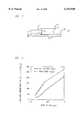
- FIG. 1is a schematic illustration of an (MOS) field effect transistor (FET).
- FIG. 2graphically illustrates that the presence of carbon in the substrate reduces dopant diffusion, and that the placement of the peak carbon concentration relative to the surface effects the degree to which the dopant diffusion is reduced.
- FIG. 1One example of a semiconductor MOSFET device is illustrated schematically in FIG. 1. That device 10 has a source region 15 and a drain region 20 formed in a silicon substrate 12. The gate 21 is formed on a gate insulator layer 22 which is formed on the silicon substrate 12. The space-charge layer 30 associated with the source region 15 and the drain region 20, while not a discrete, identifiable region in the substrate, is illustrated by the dashed line in FIG. 1. As previously noted, the space-charge layer is a function of the operating conditions. Based upon the operating conditions, the dimensions of the space-charge layer are readily ascertained by one skilled in the art.
- the devicehas a carbon-containing region 40 which has a carbon concentration that is at least 5 ⁇ 10 18 atoms/cm 3 .
- the regionis located at a depth in the substrate 12 that does not exceed about four times the depth of the source region 15 or the drain region 20 in the substrate.
- the concentration profile of the carbonis such that the concentration of carbon in the space-charge layer 30 does not exceed about 1 ⁇ 10 18 /cm -3 .
- the semiconductor material in which the carbon is introducedis either a semiconductor substrate or a semiconductor layer containing carbon incorporated therein formed on a semiconductor substrate by a chemical vapor deposition (CVD) technique as disclosed in B. Jayant Baliga, ed., "Epitaxial Silicon Technology", Academic Press (1986).
- CVDchemical vapor deposition
- Chemical vapor depositiontypically involves decomposing gaseous mixtures of a silicon-containing gas or gases on a substrate at a temperature which usually ranges from about 100° C. to about 1300° C., preferably from about 800° C. to about 1200° C., and a pressure which usually ranges from about atmospheric to about 10 mTorr.
- the substrate on which the semiconductor layer is growncan be a silicon wafer which is typically prepared by the Czochralski technique.
- the wafercan possess any suitable orientation such as an (100), (110) or (111) orientation and can be heavily or lightly doped with impurity atoms as is well known in the art.
- Background electrical doping of the semiconductor layercan be achieved by adding, for instance, traces of a suitable dopant atom-containing gas, e.g., diborane (B 2 H 6 ) or phosphine (PH 3 ), to the gaseous mixture.
- a suitable dopant atom-containing gase.g., diborane (B 2 H 6 ) or phosphine (PH 3 )
- Any suitable silicon-containing gas or mixture thereofcan be employed during CVD such as silane (SiH 4 ), disilane (Si 2 H 6 ), dichlorosilane (SiH 2 Cl 2 ), trichlorosilane (SiHCl 3 ), silicon tetrachloride (SiCl 4 ), and the like.
- a species to be incorporated within the epitaxially grown layer of siliconi.e., the carbon
- the crystal growth fluxshall be understood to refer to the species supplied to the silicon substrate in order to establish crystal growth. Carbon will occupy substitutional sites within the crystal lattice structure of the epitaxial silicon layer.
- a carbon-containing gas or mixture of carbon-containing gasesis added to the crystal growth flux during the chemical vapor deposition of an epitaxial silicon layer to thereby incorporate substitutional carbon within the deposited epitaxial silicon layer.
- substitutional carbon within such an epitaxial silicon layerhas been demonstrated to be an effective means of controlling the diffusion, i.e., the transient enhanced diffusion and dynamic clustering, of subsequently ion-implanted dopant atoms.
- One skilled in the artwill be readily able to control the epitaxial growth so that the carbon concentration does not exceed about 1 ⁇ 10 18 /cm 3 in the space charge layer and wherein the peak carbon concentration of at least about 5 ⁇ 10 18 /cm 3 is a distance from the surface of the substrate that does not exceed about four times the junction depth.
- hydrocarbonssuch as methane (CH 4 ), ethylene (C 2 H 4 ), acetylene (C 2 H 2 ) and silacyclobutane (C 3 H 6 SiH 2 ).
- the hydrocarbons employed hereinshould be of high purity, i.e., ULSI grade.
- the addition of the carbon-containing gas to the crystal growth flux during an epitaxial growth processis accomplished by adding the carbon-containing gas to the gas flow entering the CVD chamber.
- the flow rate of the gases entering the CVD chamber, including the carbon-containing gascan broadly range from about 1 standard cubic centimeter per minute (sccm) to about 10 standard liters per minute (slpm).
- substitutional carbonis incorporated in the deposited epitaxial silicon layer at a level, expressed in terms of concentration, which is at least about 5 ⁇ 10 18 C/cm 3 at a depth below the interface between the substrate and the gate dielectric layer overlying the substrate that does not exceed about four times the junction depth.
- the concentration of carbon in the space charge layeris less than about 1 ⁇ 10 18 /cm 3 .
- the concentration of substitutional carbon incorporated in the epitaxial silicon layercan be controlled, of course, by controlling the amount of carbon-containing gas which is added to the gas flow during the epitaxial growth process.
- the amount of carbon-containing gas or gases added to the gas flow during CVDis largely dependent on the reactivity of the particular carbon-containing gas being employed. For example, acetylene has been found to be more reactive under MBE conditions than ethylene. Thus, ethylene might be employed in greater amounts relative to acetylene. Suitable gases and amounts to be employed can be readily determined by routine experimentation.
- the ratio of the carbon-containing gas to the silicon-containing gaswill range from about 1:1 to about 1:10,000, with ratios ranging from about 1:100 to about 1:1000 being common.
- the amount of substitutional carbon which is incorporated in the semiconductor layercan therefore be closely controlled.
- the desired carbon concentration profileis obtained by ion implantation.
- the implant conditionsare tailored to obtain a profile in which the concentration of carbon atoms in the silicon substrate is at least about 5 ⁇ 10 18 /cm 3 at a depth in the substrate that does not exceed about four times the junction depth.
- the junction depthis the distance between the substrate surface (the substrate being the semiconductor substrate in which the various device layers are formed) and the bottom of the junction (i.e. the bottom of the source/drain regions).
- the concentration of the carbondoes not exceed about 1 ⁇ 10 18 /cm 3 either in the source or drain regions or the space charge regions adjacent to the source and drain regions of the junction.
- the substrateis annealed.
- annealsare performed at a variety of temperatures and are generally characterized as either high temperature anneals or low temperature anneals. If a high temperature anneal is used temperatures greater than 900° C. but less than about 1200° C. are contemplated as suitable.
- the annealing conditionsare selected to remove the damage caused by the carbon implant and to activate the carbon. The effect of the annealing conditions on the diffusion of boron is illustrated by the following example 1.
- Silicon substrates having a 20 nm wide boron spike with a concentration of 1 ⁇ 10 19 /cm 3were prepared by low temperature molecular beam epitaxial growth on Si(100) substrates. Carbon was implanted into silicon substrates at the energies and at the dose summarized in table 1 below. The carbon implants were subsequently annealed at two temperatures, 1050° C. for 10 seconds and 800° C. for 54 minutes, in flowing Argon.
- Siliconwas then implanted (30 KeV at a dose of 5 ⁇ 10 13 /cm 2 ) and the substrate was annealed for 35 minutes at 800° C. in Argon to imitate the transient diffusion which can occur during processing.
- the silicon implant and annealsimulates a source/drain implant plus spacer deposition and anneal in terms of the damage created by the implant and the amount of that damage that is subsequently removed by the anneal.
- Boron concentration and the depth profile of the boron spikewere measured using SIMS, and the diffusion of the boron in the substrates was thereby determined.
- the transient displacement of the boron at the various carbon implant and annealing conditionsare summarized in Table 1 below.
- Table 1illustrates that the amount of diffusion without any carbon was 26.9 nm after the low temperature anneal. That diffusion was reduced significantly by the carbon implant followed by an anneal at 1050° C. Diffusion actually increased when the carbon implant was followed by an 800° C. anneal. Therefore, the degree to which diffusion is controlled by the carbon implant depends upon the temperature at which the substrate is annealed after the carbon implant.
- Exemplary conditions for an implant that provides the desired carbon concentration profile for a device in which the edge of the space-charged layer is 0.1 ⁇ m below the surface of the substrateare enumerated in the following Table 2.
- Table 2indicates which conditions provided the desired result. These conditions are indicated as “adequate.” The conditions indicated as “too high” provided a carbon concentration that was too high. The conditions indicated as “too low” provided a carbon concentration that was too low. The conditions indicated as “too deep” provided a carbon peak concentration that was too deep. As indicated by table 2, implant dosages in the range of about 1 ⁇ 10 14 atoms/cm 2 to about 7 ⁇ 10 14 atoms/cm 2 and implant energies in the range of about 100 KeV to about 150 KeV are contemplated as suitable carbon implant conditions for devices in which the edge of the space-charge layer is 0.1 ⁇ m below the surface of the substrate.
- One skilled in the artwill be able to select suitable carbon implant conditions that provide the specified carbon concentration at the necessary depth in the substrate to satisfy the specified relationship between the carbon concentration and the depth of the space-charge layer for other devices.
- microelectronic devicescan thus be fabricated at the semiconductor layer in accordance with known methods.
- Examples of such devicesinclude MOS-type devices, e.g., n-MOS, p-MOS and CMOS devices, thin film transistors, heterojunction devices, and the like.
- FIG. 2illustrates the effect of the depth of the carbon implant in the substrate on the diffusivity of the dopants in the substrate.
- depthis the distance from the substrate surface to the peak concentration of the carbon distribution. This depth is indicated by the arrow, 42, in FIG. 1.
- D 0is the diffusivity of channel dopants in the substrate before dopants are introduced into the source and drain and D is the channel diffusivity after the dopants are introduced. D is measured at the center of the channel at the point where the local channel diffusivity is most enhanced.
- the enhancement in channel diffusivity D/D 0 due to source/drain dopantsis substantially mitigated by the introduction of a carbon layer below the junctions. As illustrated in FIG. 2, the benefit provided by the carbon layer decreased as the depth of the carbon layer in the substrate increased.
- the data depicted in FIG. 2was obtained by simulating the relationship between the depth of the dopant profile and the diffusivity enhancement for devices with a gate length of 0.25 ⁇ m and 0.5 ⁇ m.
- the benefit of the carbon implantwas proportionally greater for the 0.5 ⁇ m gate length device than for the 0.25 ⁇ m gate length device. This indicates that the degree of beneficial effect from the carbon implant is a function of channel length. That is, all other things being equal, a device with a longer channel will exhibit a greater degree of beneficial effect from the carbon implant than a device with a shorter channel.
Landscapes
- Physics & Mathematics (AREA)
- Engineering & Computer Science (AREA)
- High Energy & Nuclear Physics (AREA)
- Condensed Matter Physics & Semiconductors (AREA)
- General Physics & Mathematics (AREA)
- Manufacturing & Machinery (AREA)
- Computer Hardware Design (AREA)
- Microelectronics & Electronic Packaging (AREA)
- Power Engineering (AREA)
- Health & Medical Sciences (AREA)
- Toxicology (AREA)
- Insulated Gate Type Field-Effect Transistor (AREA)
Abstract
Description
TABLE 1 ______________________________________ Transient Displacement of Boron During Final Anneal Carbon Implant When Carbon Is Pre- When Carbon Is Pre- Conditions Annealed at 1050° C. Annealed at 800° C. ______________________________________ 150 KeV, 1 × 10.sup.14 /cm.sup.2 21.1 nm 29.7nm 100 KeV, 1 × 10.sup.14 /cm.sup.2 16.3 nm 27.6nm 150 KeV, 3 × 10.sup.14 /cm.sup.2 21 nm 30.1 nm none 26.9 nm (no anneal) ______________________________________
TABLE 2 __________________________________________________________________________ Carbon Implant Energy Carbon Dose (KeV) (1 × 10.sup.14 /cm.sup.2) 50 70 100 120 150 200 __________________________________________________________________________0.5 too high too low too low too low too low too deep 1 too high too high adequate adequate adequate too deep 1.5 too high too high adequate adequate adequate too deep 2 too high too high adequate adequate adequate too deep 3 too high too high too high adequate adequate too deep 5 too high too high too high too high adequate too deep 7 too high too high too high too high adequate too deep 9 too high too high too high too high too high too high __________________________________________________________________________
Claims (3)
Priority Applications (1)
| Application Number | Priority Date | Filing Date | Title |
|---|---|---|---|
| US09/015,981US6153920A (en) | 1994-12-01 | 1998-01-30 | Process for controlling dopant diffusion in a semiconductor layer and semiconductor device formed thereby |
Applications Claiming Priority (3)
| Application Number | Priority Date | Filing Date | Title |
|---|---|---|---|
| US34801394A | 1994-12-01 | 1994-12-01 | |
| US08/862,226US5731626A (en) | 1994-12-01 | 1997-05-23 | Process for controlling dopant diffusion in a semiconductor layer and semiconductor layer formed thereby |
| US09/015,981US6153920A (en) | 1994-12-01 | 1998-01-30 | Process for controlling dopant diffusion in a semiconductor layer and semiconductor device formed thereby |
Related Parent Applications (1)
| Application Number | Title | Priority Date | Filing Date |
|---|---|---|---|
| US08/862,226Continuation-In-PartUS5731626A (en) | 1994-12-01 | 1997-05-23 | Process for controlling dopant diffusion in a semiconductor layer and semiconductor layer formed thereby |
Publications (1)
| Publication Number | Publication Date |
|---|---|
| US6153920Atrue US6153920A (en) | 2000-11-28 |
Family
ID=26995515
Family Applications (1)
| Application Number | Title | Priority Date | Filing Date |
|---|---|---|---|
| US09/015,981Expired - LifetimeUS6153920A (en) | 1994-12-01 | 1998-01-30 | Process for controlling dopant diffusion in a semiconductor layer and semiconductor device formed thereby |
Country Status (1)
| Country | Link |
|---|---|
| US (1) | US6153920A (en) |
Cited By (75)
| Publication number | Priority date | Publication date | Assignee | Title |
|---|---|---|---|---|
| WO2002047113A3 (en)* | 2000-12-08 | 2002-08-22 | Ihp Gmbh | Layers in substrate wafers |
| US20040000691A1 (en)* | 2002-06-28 | 2004-01-01 | Karsten Wieczorek | SOI field effect transistor element having a recombination region and method of forming same |
| WO2004004015A3 (en)* | 2002-06-28 | 2004-04-08 | Advanced Micro Devices Inc | Soi field effect transistor element having a recombination region and method of forming same |
| US20040082151A1 (en)* | 2001-12-12 | 2004-04-29 | Srinivasan Chakravarthi | Fabrication of abrupt ultra-shallow junctions |
| US20040185629A1 (en)* | 2003-03-20 | 2004-09-23 | Mansoori Majid Movahed | Semiconductor device fabrication methods for inhibiting carbon out-diffusion in wafers having carbon-containing regions |
| US6806151B2 (en)* | 2001-12-14 | 2004-10-19 | Texas Instruments Incorporated | Methods and apparatus for inducing stress in a semiconductor device |
| US20050106824A1 (en)* | 2001-12-04 | 2005-05-19 | Carnera Alberto | Method for suppressing transient enhanced diffusion of dopants in silicon |
| US20050250298A1 (en)* | 2004-04-23 | 2005-11-10 | Matthias Bauer | In situ doped epitaxial films |
| US20060006427A1 (en)* | 2004-07-07 | 2006-01-12 | Tan Chung F | Material architecture for the fabrication of low temperature transistor |
| US20070096149A1 (en)* | 2005-10-31 | 2007-05-03 | Chartered Semiconductor Manufacturing, Ltd. | Implant damage control by in-situ C doping during SiGe epitaxy for device applications |
| US20070132027A1 (en)* | 2003-06-25 | 2007-06-14 | Texas Instruments Incorporated | Transistor device containing carbon doped silicon in a recess next to MDD to create strain in channel |
| US20070148888A1 (en)* | 2005-12-09 | 2007-06-28 | Krull Wade A | System and method for the manufacture of semiconductor devices by the implantation of carbon clusters |
| US20070161216A1 (en)* | 2005-12-22 | 2007-07-12 | Matthias Bauer | Epitaxial deposition of doped semiconductor materials |
| US20070164375A1 (en)* | 2006-01-16 | 2007-07-19 | Fujitsu Limited | Semiconductor device and manufacturing method thereof |
| US20080102588A1 (en)* | 2006-10-25 | 2008-05-01 | Kun-Hsien Lee | Method for forming mos transistor |
| US20080157202A1 (en)* | 2006-12-29 | 2008-07-03 | International Business Machines Corporation | Soft error reduction of cmos circuits on substrates with hybrid crystal orientation using buried recombination centers |
| US20080185636A1 (en)* | 2007-02-07 | 2008-08-07 | International Business Machines Corporation | Semiconductor structure including doped silicon carbon liner layer and method for fabrication thereof |
| US20080299749A1 (en)* | 2006-12-06 | 2008-12-04 | Jacobson Dale C | Cluster ion implantation for defect engineering |
| US20090302381A1 (en)* | 2007-12-14 | 2009-12-10 | James Pan | Structure and Method for Forming Power Devices with Carbon-containing Region |
| US20100084706A1 (en)* | 2003-05-20 | 2010-04-08 | Kocon Christopher B | Power Semiconductor Devices and Methods of Manufacture |
| WO2012050653A1 (en)* | 2010-10-15 | 2012-04-19 | International Business Machines Corporation | METHOD AND STRUCTURE FOR pFET JUNCTION PROFILE WITH SiGe CHANNEL |
| US8319290B2 (en) | 2010-06-18 | 2012-11-27 | Fairchild Semiconductor Corporation | Trench MOS barrier schottky rectifier with a planar surface using CMP techniques |
| US20130062623A1 (en)* | 2011-09-09 | 2013-03-14 | Kabushiki Kaisha Toshiba | Semiconductor device and method of manufacturing the same |
| US8404551B2 (en) | 2010-12-03 | 2013-03-26 | Suvolta, Inc. | Source/drain extension control for advanced transistors |
| US8421162B2 (en) | 2009-09-30 | 2013-04-16 | Suvolta, Inc. | Advanced transistors with punch through suppression |
| US8461875B1 (en) | 2011-02-18 | 2013-06-11 | Suvolta, Inc. | Digital circuits having improved transistors, and methods therefor |
| US8525271B2 (en) | 2011-03-03 | 2013-09-03 | Suvolta, Inc. | Semiconductor structure with improved channel stack and method for fabrication thereof |
| US8530286B2 (en) | 2010-04-12 | 2013-09-10 | Suvolta, Inc. | Low power semiconductor transistor structure and method of fabrication thereof |
| US8569128B2 (en) | 2010-06-21 | 2013-10-29 | Suvolta, Inc. | Semiconductor structure and method of fabrication thereof with mixed metal types |
| US8569156B1 (en) | 2011-05-16 | 2013-10-29 | Suvolta, Inc. | Reducing or eliminating pre-amorphization in transistor manufacture |
| US8599623B1 (en) | 2011-12-23 | 2013-12-03 | Suvolta, Inc. | Circuits and methods for measuring circuit elements in an integrated circuit device |
| US8614128B1 (en) | 2011-08-23 | 2013-12-24 | Suvolta, Inc. | CMOS structures and processes based on selective thinning |
| US8629016B1 (en) | 2011-07-26 | 2014-01-14 | Suvolta, Inc. | Multiple transistor types formed in a common epitaxial layer by differential out-diffusion from a doped underlayer |
| US8637955B1 (en) | 2012-08-31 | 2014-01-28 | Suvolta, Inc. | Semiconductor structure with reduced junction leakage and method of fabrication thereof |
| US8645878B1 (en) | 2011-08-23 | 2014-02-04 | Suvolta, Inc. | Porting a circuit design from a first semiconductor process to a second semiconductor process |
| US8713511B1 (en) | 2011-09-16 | 2014-04-29 | Suvolta, Inc. | Tools and methods for yield-aware semiconductor manufacturing process target generation |
| US8735987B1 (en) | 2011-06-06 | 2014-05-27 | Suvolta, Inc. | CMOS gate stack structures and processes |
| US8748986B1 (en) | 2011-08-05 | 2014-06-10 | Suvolta, Inc. | Electronic device with controlled threshold voltage |
| US8748270B1 (en) | 2011-03-30 | 2014-06-10 | Suvolta, Inc. | Process for manufacturing an improved analog transistor |
| US20140158938A1 (en)* | 2005-01-20 | 2014-06-12 | Samsung Electronics Co., Ltd | Quantum dot phosphor for light emitting diode and method of preparing the same |
| US8759872B2 (en) | 2010-06-22 | 2014-06-24 | Suvolta, Inc. | Transistor with threshold voltage set notch and method of fabrication thereof |
| US8796048B1 (en) | 2011-05-11 | 2014-08-05 | Suvolta, Inc. | Monitoring and measurement of thin film layers |
| US8811068B1 (en) | 2011-05-13 | 2014-08-19 | Suvolta, Inc. | Integrated circuit devices and methods |
| US8816754B1 (en) | 2012-11-02 | 2014-08-26 | Suvolta, Inc. | Body bias circuits and methods |
| US8819603B1 (en) | 2011-12-15 | 2014-08-26 | Suvolta, Inc. | Memory circuits and methods of making and designing the same |
| US8863064B1 (en) | 2012-03-23 | 2014-10-14 | Suvolta, Inc. | SRAM cell layout structure and devices therefrom |
| US8877619B1 (en) | 2012-01-23 | 2014-11-04 | Suvolta, Inc. | Process for manufacture of integrated circuits with different channel doping transistor architectures and devices therefrom |
| US8883600B1 (en) | 2011-12-22 | 2014-11-11 | Suvolta, Inc. | Transistor having reduced junction leakage and methods of forming thereof |
| US8895327B1 (en) | 2011-12-09 | 2014-11-25 | Suvolta, Inc. | Tipless transistors, short-tip transistors, and methods and circuits therefor |
| US20150024569A1 (en)* | 2011-08-16 | 2015-01-22 | Taiwan Semiconductor Manufacturing Company, Ltd. | Integrated circuits and methods of forming integrated circuits |
| US8962417B2 (en) | 2010-10-15 | 2015-02-24 | International Business Machines Corporation | Method and structure for pFET junction profile with SiGe channel |
| US8963212B2 (en) | 2008-12-08 | 2015-02-24 | Fairchild Semiconductor Corporation | Trench-based power semiconductor devices with increased breakdown voltage characteristics |
| US8970289B1 (en) | 2012-01-23 | 2015-03-03 | Suvolta, Inc. | Circuits and devices for generating bi-directional body bias voltages, and methods therefor |
| US8995204B2 (en) | 2011-06-23 | 2015-03-31 | Suvolta, Inc. | Circuit devices and methods having adjustable transistor body bias |
| US8999861B1 (en) | 2011-05-11 | 2015-04-07 | Suvolta, Inc. | Semiconductor structure with substitutional boron and method for fabrication thereof |
| US9041126B2 (en) | 2012-09-21 | 2015-05-26 | Mie Fujitsu Semiconductor Limited | Deeply depleted MOS transistors having a screening layer and methods thereof |
| US9054219B1 (en) | 2011-08-05 | 2015-06-09 | Mie Fujitsu Semiconductor Limited | Semiconductor devices having fin structures and fabrication methods thereof |
| US9070477B1 (en) | 2012-12-12 | 2015-06-30 | Mie Fujitsu Semiconductor Limited | Bit interleaved low voltage static random access memory (SRAM) and related methods |
| US9093997B1 (en) | 2012-11-15 | 2015-07-28 | Mie Fujitsu Semiconductor Limited | Slew based process and bias monitors and related methods |
| US9093550B1 (en) | 2012-01-31 | 2015-07-28 | Mie Fujitsu Semiconductor Limited | Integrated circuits having a plurality of high-K metal gate FETs with various combinations of channel foundation structure and gate stack structure and methods of making same |
| US9112057B1 (en) | 2012-09-18 | 2015-08-18 | Mie Fujitsu Semiconductor Limited | Semiconductor devices with dopant migration suppression and method of fabrication thereof |
| US9112484B1 (en) | 2012-12-20 | 2015-08-18 | Mie Fujitsu Semiconductor Limited | Integrated circuit process and bias monitors and related methods |
| US9236466B1 (en) | 2011-10-07 | 2016-01-12 | Mie Fujitsu Semiconductor Limited | Analog circuits having improved insulated gate transistors, and methods therefor |
| US9268885B1 (en) | 2013-02-28 | 2016-02-23 | Mie Fujitsu Semiconductor Limited | Integrated circuit device methods and models with predicted device metric variations |
| US9299698B2 (en) | 2012-06-27 | 2016-03-29 | Mie Fujitsu Semiconductor Limited | Semiconductor structure with multiple transistors having various threshold voltages |
| US9319013B2 (en) | 2014-08-19 | 2016-04-19 | Mie Fujitsu Semiconductor Limited | Operational amplifier input offset correction with transistor threshold voltage adjustment |
| CN105529268A (en)* | 2014-10-27 | 2016-04-27 | 中芯国际集成电路制造(上海)有限公司 | Transistor and forming method thereof |
| US9406567B1 (en) | 2012-02-28 | 2016-08-02 | Mie Fujitsu Semiconductor Limited | Method for fabricating multiple transistor devices on a substrate with varying threshold voltages |
| US9431068B2 (en) | 2012-10-31 | 2016-08-30 | Mie Fujitsu Semiconductor Limited | Dynamic random access memory (DRAM) with low variation transistor peripheral circuits |
| US9478571B1 (en) | 2013-05-24 | 2016-10-25 | Mie Fujitsu Semiconductor Limited | Buried channel deeply depleted channel transistor |
| US9577041B2 (en) | 2013-03-14 | 2017-02-21 | Mie Fujitsu Semiconductor Limited | Method for fabricating a transistor device with a tuned dopant profile |
| US9710006B2 (en) | 2014-07-25 | 2017-07-18 | Mie Fujitsu Semiconductor Limited | Power up body bias circuits and methods |
| US10074568B2 (en) | 2009-09-30 | 2018-09-11 | Mie Fujitsu Semiconductor Limited | Electronic devices and systems, and methods for making and using same |
| CN113437078A (en)* | 2020-03-23 | 2021-09-24 | 铠侠股份有限公司 | Semiconductor memory device and method of manufacturing the same |
| US11621168B1 (en) | 2022-07-12 | 2023-04-04 | Gyrotron Technology, Inc. | Method and system for doping semiconductor materials |
Citations (3)
| Publication number | Priority date | Publication date | Assignee | Title |
|---|---|---|---|---|
| US5116455A (en)* | 1991-01-24 | 1992-05-26 | Spire Corporation | Process of making strain-free, carbon-doped epitaxial layers and products so made |
| US5338945A (en)* | 1993-01-25 | 1994-08-16 | North Carolina State University At Raleigh | Silicon carbide field effect transistor |
| US5731626A (en)* | 1994-12-01 | 1998-03-24 | Lucent Technologies Inc. | Process for controlling dopant diffusion in a semiconductor layer and semiconductor layer formed thereby |
- 1998
- 1998-01-30USUS09/015,981patent/US6153920A/ennot_activeExpired - Lifetime
Patent Citations (4)
| Publication number | Priority date | Publication date | Assignee | Title |
|---|---|---|---|---|
| US5116455A (en)* | 1991-01-24 | 1992-05-26 | Spire Corporation | Process of making strain-free, carbon-doped epitaxial layers and products so made |
| US5338945A (en)* | 1993-01-25 | 1994-08-16 | North Carolina State University At Raleigh | Silicon carbide field effect transistor |
| US5731626A (en)* | 1994-12-01 | 1998-03-24 | Lucent Technologies Inc. | Process for controlling dopant diffusion in a semiconductor layer and semiconductor layer formed thereby |
| US6043139A (en)* | 1994-12-01 | 2000-03-28 | Lucent Technologies Inc. | Process for controlling dopant diffusion in a semiconductor layer |
Non-Patent Citations (12)
| Title |
|---|
| "Dislocation Formation and B Transient Diffusion in C Coimplanted Si", by Cacciato, A. et al., J. Appl. Phys., 79(5) pp. 2314-2325 (Mar. 1, 1996). |
| "Effects of Low Dose Silicon, Carbon, and Oxygen Implantation Damage on Diffusion of Phosphorous in Silicon", by Chaudhry, S. et al., J. Electrochem. Soc., vol. 141, No. 12, pp. 3516-3521 (Dec. 1994). |
| "Reduction of Transient Boron Diffusion in Preamorphized Si by Carbon Implantation", by Nishikawa, S. et al., Appl. Phys. Lett., 60 (18), pp. 2270-2272 (May 4, 1992). |
| "Role of C and B Clusters in Transient Diffusion of B in Silicon", by Cowern, N. E. B. et al., Appl. Phys. Lett., 68 (8), pp. 1150-1152 (Nov. 6, 1995). |
| "Suppression of Dislocation Formation in Silicon by Carbon Implantation", by Simpson, T. W. et al., Appl. Phys. Lett., pp. 2857-2859 (Nov. 6, 1995). |
| "Suppression of Oxidation-Enhanced Boron Diffusion in Silicon by Carbon Implantation and Characterization of MOSFET's with Carbon-Implanted Channels", by Ban, I. et al., IEEE Transactions on Electron Devices, vol. 44, No. 9 pp. 1544-1551 (Sep. 1997). |
| Dislocation Formation and B Transient Diffusion in C Coimplanted Si , by Cacciato, A. et al., J. Appl. Phys. , 79(5) pp. 2314 2325 (Mar. 1, 1996).* |
| Effects of Low Dose Silicon, Carbon, and Oxygen Implantation Damage on Diffusion of Phosphorous in Silicon , by Chaudhry, S. et al., J. Electrochem. Soc. , vol. 141, No. 12, pp. 3516 3521 (Dec. 1994).* |
| Reduction of Transient Boron Diffusion in Preamorphized Si by Carbon Implantation , by Nishikawa, S. et al., Appl. Phys. Lett. , 60 (18), pp. 2270 2272 (May 4, 1992).* |
| Role of C and B Clusters in Transient Diffusion of B in Silicon , by Cowern, N. E. B. et al., Appl. Phys. Lett. , 68 (8), pp. 1150 1152 (Nov. 6, 1995).* |
| Suppression of Dislocation Formation in Silicon by Carbon Implantation , by Simpson, T. W. et al., Appl. Phys. Lett. , pp. 2857 2859 (Nov. 6, 1995).* |
| Suppression of Oxidation Enhanced Boron Diffusion in Silicon by Carbon Implantation and Characterization of MOSFET s with Carbon Implanted Channels , by Ban, I. et al., IEEE Transactions on Electron Devices , vol. 44, No. 9 pp. 1544 1551 (Sep. 1997).* |
Cited By (172)
| Publication number | Priority date | Publication date | Assignee | Title |
|---|---|---|---|---|
| WO2002047113A3 (en)* | 2000-12-08 | 2002-08-22 | Ihp Gmbh | Layers in substrate wafers |
| US20040075118A1 (en)* | 2000-12-08 | 2004-04-22 | Bernd Heinemann | Layers in substrate wafers |
| US7595534B2 (en) | 2000-12-08 | 2009-09-29 | Ihp Gmbh-Innovations For High Performance Microelectronics/Institut Fur Innovative Mikroelektronik | Layers in substrate wafers |
| US9368587B2 (en) | 2001-01-30 | 2016-06-14 | Fairchild Semiconductor Corporation | Accumulation-mode field effect transistor with improved current capability |
| US20050106824A1 (en)* | 2001-12-04 | 2005-05-19 | Carnera Alberto | Method for suppressing transient enhanced diffusion of dopants in silicon |
| US20040082151A1 (en)* | 2001-12-12 | 2004-04-29 | Srinivasan Chakravarthi | Fabrication of abrupt ultra-shallow junctions |
| US7112516B2 (en)* | 2001-12-12 | 2006-09-26 | Texas Instruments Incorporated | Fabrication of abrupt ultra-shallow junctions |
| US7339214B2 (en) | 2001-12-14 | 2008-03-04 | Texas Instruments Incorporated | Methods and apparatus for inducing stress in a semiconductor device |
| US6806151B2 (en)* | 2001-12-14 | 2004-10-19 | Texas Instruments Incorporated | Methods and apparatus for inducing stress in a semiconductor device |
| US20050029560A1 (en)* | 2001-12-14 | 2005-02-10 | Christoph Wasshuber | Methods and apparatus for inducing stress in a semiconductor device |
| US6812074B2 (en) | 2002-06-28 | 2004-11-02 | Advanced Micro Devices, Inc. | SOI field effect transistor element having a recombination region and method of forming same |
| WO2004004015A3 (en)* | 2002-06-28 | 2004-04-08 | Advanced Micro Devices Inc | Soi field effect transistor element having a recombination region and method of forming same |
| US20040000691A1 (en)* | 2002-06-28 | 2004-01-01 | Karsten Wieczorek | SOI field effect transistor element having a recombination region and method of forming same |
| US20050037548A1 (en)* | 2002-06-28 | 2005-02-17 | Advanced Micro Devices, Inc. | SOI field effect transistor element having a recombination region and method of forming same |
| EP1463101A3 (en)* | 2003-03-20 | 2010-08-25 | Texas Instruments Incorporated | Semiconductor device fabrication methods for inhibiting carbon out-diffusion from the semiconductor wafer |
| US6830980B2 (en)* | 2003-03-20 | 2004-12-14 | Texas Instruments Incorporated | Semiconductor device fabrication methods for inhibiting carbon out-diffusion in wafers having carbon-containing regions |
| US20040185629A1 (en)* | 2003-03-20 | 2004-09-23 | Mansoori Majid Movahed | Semiconductor device fabrication methods for inhibiting carbon out-diffusion in wafers having carbon-containing regions |
| US8889511B2 (en) | 2003-05-20 | 2014-11-18 | Fairchild Semiconductor Corporation | Methods of manufacturing power semiconductor devices with trenched shielded split gate transistor |
| US8350317B2 (en) | 2003-05-20 | 2013-01-08 | Fairchild Semiconductor Corporation | Power semiconductor devices and methods of manufacture |
| US8936985B2 (en) | 2003-05-20 | 2015-01-20 | Fairchild Semiconductor Corporation | Methods related to power semiconductor devices with thick bottom oxide layers |
| US8143124B2 (en) | 2003-05-20 | 2012-03-27 | Fairchild Semiconductor Corporation | Methods of making power semiconductor devices with thick bottom oxide layer |
| US8786045B2 (en) | 2003-05-20 | 2014-07-22 | Fairchild Semiconductor Corporation | Power semiconductor devices having termination structures |
| US8129245B2 (en) | 2003-05-20 | 2012-03-06 | Fairchild Semiconductor Corporation | Methods of manufacturing power semiconductor devices with shield and gate contacts |
| US8013387B2 (en) | 2003-05-20 | 2011-09-06 | Fairchild Semiconductor Corporation | Power semiconductor devices with shield and gate contacts and methods of manufacture |
| US7982265B2 (en) | 2003-05-20 | 2011-07-19 | Fairchild Semiconductor Corporation | Trenched shield gate power semiconductor devices and methods of manufacture |
| US20100084706A1 (en)* | 2003-05-20 | 2010-04-08 | Kocon Christopher B | Power Semiconductor Devices and Methods of Manufacture |
| US20070132027A1 (en)* | 2003-06-25 | 2007-06-14 | Texas Instruments Incorporated | Transistor device containing carbon doped silicon in a recess next to MDD to create strain in channel |
| US7339215B2 (en)* | 2003-06-25 | 2008-03-04 | Texas Instruments Incorporated | Transistor device containing carbon doped silicon in a recess next to MDD to create strain in channel |
| US20050250298A1 (en)* | 2004-04-23 | 2005-11-10 | Matthias Bauer | In situ doped epitaxial films |
| US20070117326A1 (en)* | 2004-07-07 | 2007-05-24 | Tan Chung F | Material architecture for the fabrication of low temperature transistor |
| US20060006427A1 (en)* | 2004-07-07 | 2006-01-12 | Tan Chung F | Material architecture for the fabrication of low temperature transistor |
| US7169675B2 (en) | 2004-07-07 | 2007-01-30 | Chartered Semiconductor Manufacturing, Ltd | Material architecture for the fabrication of low temperature transistor |
| US20140158938A1 (en)* | 2005-01-20 | 2014-06-12 | Samsung Electronics Co., Ltd | Quantum dot phosphor for light emitting diode and method of preparing the same |
| US9475984B2 (en)* | 2005-01-20 | 2016-10-25 | Samsung Electronics Co., Ltd. | Quantum dot phosphor for light emitting diode and method of preparing the same |
| US9902902B2 (en) | 2005-01-20 | 2018-02-27 | Samsung Electronics Co., Ltd. | Quantum dot phosphor for light emitting diode and method of preparing the same |
| US20110223737A1 (en)* | 2005-10-31 | 2011-09-15 | Globalfoundries Singapore Pte. Ltd. | Implant damage control by in-situ c doping during sige epitaxy for device applications |
| US8652892B2 (en) | 2005-10-31 | 2014-02-18 | International Business Machines Corporation (Ibm) | Implant damage control by in-situ C doping during sige epitaxy for device applications |
| US8790980B2 (en) | 2005-10-31 | 2014-07-29 | International Business Machines Corporation (Ibm) | Implant damage control by in-situ C doping during sige epitaxy for device applications |
| US20070096149A1 (en)* | 2005-10-31 | 2007-05-03 | Chartered Semiconductor Manufacturing, Ltd. | Implant damage control by in-situ C doping during SiGe epitaxy for device applications |
| US7947546B2 (en)* | 2005-10-31 | 2011-05-24 | Chartered Semiconductor Manufacturing, Ltd. | Implant damage control by in-situ C doping during SiGe epitaxy for device applications |
| US7666771B2 (en) | 2005-12-09 | 2010-02-23 | Semequip, Inc. | System and method for the manufacture of semiconductor devices by the implantation of carbon clusters |
| US8530343B2 (en) | 2005-12-09 | 2013-09-10 | Semequip, Inc. | System and method for the manufacture of semiconductor devices by the implantation of carbon clusters |
| US20090286367A1 (en)* | 2005-12-09 | 2009-11-19 | Krull Wade A | System and method for the manufacture of semiconductor devices by the implantation of carbon clusters |
| US20070148888A1 (en)* | 2005-12-09 | 2007-06-28 | Krull Wade A | System and method for the manufacture of semiconductor devices by the implantation of carbon clusters |
| US8097529B2 (en) | 2005-12-09 | 2012-01-17 | Semequip, Inc. | System and method for the manufacture of semiconductor devices by the implantation of carbon clusters |
| US20070161216A1 (en)* | 2005-12-22 | 2007-07-12 | Matthias Bauer | Epitaxial deposition of doped semiconductor materials |
| US7863163B2 (en)* | 2005-12-22 | 2011-01-04 | Asm America, Inc. | Epitaxial deposition of doped semiconductor materials |
| US20100003798A1 (en)* | 2006-01-16 | 2010-01-07 | Fujitsu Microelectronics Limited | Semiconductor device and manufacturing method thereof |
| US7601996B2 (en)* | 2006-01-16 | 2009-10-13 | Fujitsu Microelectronics Limited | Semiconductor device and manufacturing method thereof |
| US7838401B2 (en) | 2006-01-16 | 2010-11-23 | Fujitsu Semiconductor Limited | Semiconductor device and manufacturing method thereof |
| US20070164375A1 (en)* | 2006-01-16 | 2007-07-19 | Fujitsu Limited | Semiconductor device and manufacturing method thereof |
| US20080102588A1 (en)* | 2006-10-25 | 2008-05-01 | Kun-Hsien Lee | Method for forming mos transistor |
| US20080299749A1 (en)* | 2006-12-06 | 2008-12-04 | Jacobson Dale C | Cluster ion implantation for defect engineering |
| US7919402B2 (en) | 2006-12-06 | 2011-04-05 | Semequip, Inc. | Cluster ion implantation for defect engineering |
| US7521776B2 (en) | 2006-12-29 | 2009-04-21 | International Business Machines Corporation | Soft error reduction of CMOS circuits on substrates with hybrid crystal orientation using buried recombination centers |
| US20080157202A1 (en)* | 2006-12-29 | 2008-07-03 | International Business Machines Corporation | Soft error reduction of cmos circuits on substrates with hybrid crystal orientation using buried recombination centers |
| US20080185636A1 (en)* | 2007-02-07 | 2008-08-07 | International Business Machines Corporation | Semiconductor structure including doped silicon carbon liner layer and method for fabrication thereof |
| US7667263B2 (en) | 2007-02-07 | 2010-02-23 | International Business Machines Corporation | Semiconductor structure including doped silicon carbon liner layer and method for fabrication thereof |
| US20090302381A1 (en)* | 2007-12-14 | 2009-12-10 | James Pan | Structure and Method for Forming Power Devices with Carbon-containing Region |
| US7994573B2 (en)* | 2007-12-14 | 2011-08-09 | Fairchild Semiconductor Corporation | Structure and method for forming power devices with carbon-containing region |
| US9391193B2 (en) | 2008-12-08 | 2016-07-12 | Fairchild Semiconductor Corporation | Trench-based power semiconductor devices with increased breakdown voltage characteristics |
| US8963212B2 (en) | 2008-12-08 | 2015-02-24 | Fairchild Semiconductor Corporation | Trench-based power semiconductor devices with increased breakdown voltage characteristics |
| US11887895B2 (en) | 2009-09-30 | 2024-01-30 | United Semiconductor Japan Co., Ltd. | Electronic devices and systems, and methods for making and using the same |
| US9508800B2 (en) | 2009-09-30 | 2016-11-29 | Mie Fujitsu Semiconductor Limited | Advanced transistors with punch through suppression |
| US11062950B2 (en) | 2009-09-30 | 2021-07-13 | United Semiconductor Japan Co., Ltd. | Electronic devices and systems, and methods for making and using the same |
| US10325986B2 (en) | 2009-09-30 | 2019-06-18 | Mie Fujitsu Semiconductor Limited | Advanced transistors with punch through suppression |
| US8421162B2 (en) | 2009-09-30 | 2013-04-16 | Suvolta, Inc. | Advanced transistors with punch through suppression |
| US10224244B2 (en) | 2009-09-30 | 2019-03-05 | Mie Fujitsu Semiconductor Limited | Electronic devices and systems, and methods for making and using the same |
| US10217668B2 (en) | 2009-09-30 | 2019-02-26 | Mie Fujitsu Semiconductor Limited | Electronic devices and systems, and methods for making and using the same |
| US10074568B2 (en) | 2009-09-30 | 2018-09-11 | Mie Fujitsu Semiconductor Limited | Electronic devices and systems, and methods for making and using same |
| US9263523B2 (en) | 2009-09-30 | 2016-02-16 | Mie Fujitsu Semiconductor Limited | Advanced transistors with punch through suppression |
| US9865596B2 (en) | 2010-04-12 | 2018-01-09 | Mie Fujitsu Semiconductor Limited | Low power semiconductor transistor structure and method of fabrication thereof |
| US8530286B2 (en) | 2010-04-12 | 2013-09-10 | Suvolta, Inc. | Low power semiconductor transistor structure and method of fabrication thereof |
| US9496261B2 (en) | 2010-04-12 | 2016-11-15 | Mie Fujitsu Semiconductor Limited | Low power semiconductor transistor structure and method of fabrication thereof |
| US8319290B2 (en) | 2010-06-18 | 2012-11-27 | Fairchild Semiconductor Corporation | Trench MOS barrier schottky rectifier with a planar surface using CMP techniques |
| US8432000B2 (en) | 2010-06-18 | 2013-04-30 | Fairchild Semiconductor Corporation | Trench MOS barrier schottky rectifier with a planar surface using CMP techniques |
| US8569128B2 (en) | 2010-06-21 | 2013-10-29 | Suvolta, Inc. | Semiconductor structure and method of fabrication thereof with mixed metal types |
| US9224733B2 (en) | 2010-06-21 | 2015-12-29 | Mie Fujitsu Semiconductor Limited | Semiconductor structure and method of fabrication thereof with mixed metal types |
| US8759872B2 (en) | 2010-06-22 | 2014-06-24 | Suvolta, Inc. | Transistor with threshold voltage set notch and method of fabrication thereof |
| US9922977B2 (en) | 2010-06-22 | 2018-03-20 | Mie Fujitsu Semiconductor Limited | Transistor with threshold voltage set notch and method of fabrication thereof |
| US9418987B2 (en) | 2010-06-22 | 2016-08-16 | Mie Fujitsu Semiconductor Limited | Transistor with threshold voltage set notch and method of fabrication thereof |
| GB2497060A (en)* | 2010-10-15 | 2013-05-29 | Ibm | Method and structure for pFET junction profile with SiGe channel |
| WO2012050653A1 (en)* | 2010-10-15 | 2012-04-19 | International Business Machines Corporation | METHOD AND STRUCTURE FOR pFET JUNCTION PROFILE WITH SiGe CHANNEL |
| US8962417B2 (en) | 2010-10-15 | 2015-02-24 | International Business Machines Corporation | Method and structure for pFET junction profile with SiGe channel |
| US8659054B2 (en) | 2010-10-15 | 2014-02-25 | International Business Machines Corporation | Method and structure for pFET junction profile with SiGe channel |
| GB2497060B (en)* | 2010-10-15 | 2013-10-09 | Ibm | Method and structure for pFET junction profile with SiGe channel |
| US9006843B2 (en) | 2010-12-03 | 2015-04-14 | Suvolta, Inc. | Source/drain extension control for advanced transistors |
| US8563384B2 (en) | 2010-12-03 | 2013-10-22 | Suvolta, Inc. | Source/drain extension control for advanced transistors |
| US8686511B2 (en) | 2010-12-03 | 2014-04-01 | Suvolta, Inc. | Source/drain extension control for advanced transistors |
| US8404551B2 (en) | 2010-12-03 | 2013-03-26 | Suvolta, Inc. | Source/drain extension control for advanced transistors |
| US9680470B2 (en) | 2011-02-18 | 2017-06-13 | Mie Fujitsu Semiconductor Limited | Digital circuits having improved transistors, and methods therefor |
| US8461875B1 (en) | 2011-02-18 | 2013-06-11 | Suvolta, Inc. | Digital circuits having improved transistors, and methods therefor |
| US9985631B2 (en) | 2011-02-18 | 2018-05-29 | Mie Fujitsu Semiconductor Limited | Digital circuits having improved transistors, and methods therefor |
| US9184750B1 (en) | 2011-02-18 | 2015-11-10 | Mie Fujitsu Semiconductor Limited | Digital circuits having improved transistors, and methods therefor |
| US9838012B2 (en) | 2011-02-18 | 2017-12-05 | Mie Fujitsu Semiconductor Limited | Digital circuits having improved transistors, and methods therefor |
| US10250257B2 (en) | 2011-02-18 | 2019-04-02 | Mie Fujitsu Semiconductor Limited | Digital circuits having improved transistors, and methods therefor |
| US8525271B2 (en) | 2011-03-03 | 2013-09-03 | Suvolta, Inc. | Semiconductor structure with improved channel stack and method for fabrication thereof |
| US9111785B2 (en) | 2011-03-03 | 2015-08-18 | Mie Fujitsu Semiconductor Limited | Semiconductor structure with improved channel stack and method for fabrication thereof |
| US8748270B1 (en) | 2011-03-30 | 2014-06-10 | Suvolta, Inc. | Process for manufacturing an improved analog transistor |
| US9093469B2 (en) | 2011-03-30 | 2015-07-28 | Mie Fujitsu Semiconductor Limited | Analog transistor |
| US8999861B1 (en) | 2011-05-11 | 2015-04-07 | Suvolta, Inc. | Semiconductor structure with substitutional boron and method for fabrication thereof |
| US8796048B1 (en) | 2011-05-11 | 2014-08-05 | Suvolta, Inc. | Monitoring and measurement of thin film layers |
| US9362291B1 (en) | 2011-05-13 | 2016-06-07 | Mie Fujitsu Semiconductor Limited | Integrated circuit devices and methods |
| US9741428B2 (en) | 2011-05-13 | 2017-08-22 | Mie Fujitsu Semiconductor Limited | Integrated circuit devices and methods |
| US9966130B2 (en) | 2011-05-13 | 2018-05-08 | Mie Fujitsu Semiconductor Limited | Integrated circuit devices and methods |
| US8811068B1 (en) | 2011-05-13 | 2014-08-19 | Suvolta, Inc. | Integrated circuit devices and methods |
| US8937005B2 (en) | 2011-05-16 | 2015-01-20 | Suvolta, Inc. | Reducing or eliminating pre-amorphization in transistor manufacture |
| US9793172B2 (en) | 2011-05-16 | 2017-10-17 | Mie Fujitsu Semiconductor Limited | Reducing or eliminating pre-amorphization in transistor manufacture |
| US8569156B1 (en) | 2011-05-16 | 2013-10-29 | Suvolta, Inc. | Reducing or eliminating pre-amorphization in transistor manufacture |
| US9514940B2 (en) | 2011-05-16 | 2016-12-06 | Mie Fujitsu Semiconductor Limited | Reducing or eliminating pre-amorphization in transistor manufacture |
| US8735987B1 (en) | 2011-06-06 | 2014-05-27 | Suvolta, Inc. | CMOS gate stack structures and processes |
| US9281248B1 (en) | 2011-06-06 | 2016-03-08 | Mie Fujitsu Semiconductor Limited | CMOS gate stack structures and processes |
| US8995204B2 (en) | 2011-06-23 | 2015-03-31 | Suvolta, Inc. | Circuit devices and methods having adjustable transistor body bias |
| US8653604B1 (en) | 2011-07-26 | 2014-02-18 | Suvolta, Inc. | Multiple transistor types formed in a common epitaxial layer by differential out-diffusion from a doped underlayer |
| US8629016B1 (en) | 2011-07-26 | 2014-01-14 | Suvolta, Inc. | Multiple transistor types formed in a common epitaxial layer by differential out-diffusion from a doped underlayer |
| US8916937B1 (en) | 2011-07-26 | 2014-12-23 | Suvolta, Inc. | Multiple transistor types formed in a common epitaxial layer by differential out-diffusion from a doped underlayer |
| US9054219B1 (en) | 2011-08-05 | 2015-06-09 | Mie Fujitsu Semiconductor Limited | Semiconductor devices having fin structures and fabrication methods thereof |
| US8963249B1 (en) | 2011-08-05 | 2015-02-24 | Suvolta, Inc. | Electronic device with controlled threshold voltage |
| US8748986B1 (en) | 2011-08-05 | 2014-06-10 | Suvolta, Inc. | Electronic device with controlled threshold voltage |
| US9865732B2 (en) | 2011-08-16 | 2018-01-09 | Taiwan Semiconductor Manufacturing Company, Ltd. | Integrated circuits and methods of forming integrated circuits |
| US20150024569A1 (en)* | 2011-08-16 | 2015-01-22 | Taiwan Semiconductor Manufacturing Company, Ltd. | Integrated circuits and methods of forming integrated circuits |
| US9379208B2 (en)* | 2011-08-16 | 2016-06-28 | Taiwan Semiconductor Manufacturing Company, Ltd. | Integrated circuits and methods of forming integrated circuits |
| US8806395B1 (en) | 2011-08-23 | 2014-08-12 | Suvolta, Inc. | Porting a circuit design from a first semiconductor process to a second semiconductor process |
| US9117746B1 (en) | 2011-08-23 | 2015-08-25 | Mie Fujitsu Semiconductor Limited | Porting a circuit design from a first semiconductor process to a second semiconductor process |
| US8645878B1 (en) | 2011-08-23 | 2014-02-04 | Suvolta, Inc. | Porting a circuit design from a first semiconductor process to a second semiconductor process |
| US8614128B1 (en) | 2011-08-23 | 2013-12-24 | Suvolta, Inc. | CMOS structures and processes based on selective thinning |
| US9391076B1 (en) | 2011-08-23 | 2016-07-12 | Mie Fujitsu Semiconductor Limited | CMOS structures and processes based on selective thinning |
| US8994034B2 (en)* | 2011-09-09 | 2015-03-31 | Kabushiki Kaisha Toshiba | Semiconductor device and method of manufacturing the same |
| US20130062623A1 (en)* | 2011-09-09 | 2013-03-14 | Kabushiki Kaisha Toshiba | Semiconductor device and method of manufacturing the same |
| US8713511B1 (en) | 2011-09-16 | 2014-04-29 | Suvolta, Inc. | Tools and methods for yield-aware semiconductor manufacturing process target generation |
| US9236466B1 (en) | 2011-10-07 | 2016-01-12 | Mie Fujitsu Semiconductor Limited | Analog circuits having improved insulated gate transistors, and methods therefor |
| US8895327B1 (en) | 2011-12-09 | 2014-11-25 | Suvolta, Inc. | Tipless transistors, short-tip transistors, and methods and circuits therefor |
| US8819603B1 (en) | 2011-12-15 | 2014-08-26 | Suvolta, Inc. | Memory circuits and methods of making and designing the same |
| US8883600B1 (en) | 2011-12-22 | 2014-11-11 | Suvolta, Inc. | Transistor having reduced junction leakage and methods of forming thereof |
| US9368624B2 (en) | 2011-12-22 | 2016-06-14 | Mie Fujitsu Semiconductor Limited | Method for fabricating a transistor with reduced junction leakage current |
| US9196727B2 (en) | 2011-12-22 | 2015-11-24 | Mie Fujitsu Semiconductor Limited | High uniformity screen and epitaxial layers for CMOS devices |
| US8599623B1 (en) | 2011-12-23 | 2013-12-03 | Suvolta, Inc. | Circuits and methods for measuring circuit elements in an integrated circuit device |
| US8970289B1 (en) | 2012-01-23 | 2015-03-03 | Suvolta, Inc. | Circuits and devices for generating bi-directional body bias voltages, and methods therefor |
| US8877619B1 (en) | 2012-01-23 | 2014-11-04 | Suvolta, Inc. | Process for manufacture of integrated circuits with different channel doping transistor architectures and devices therefrom |
| US9093550B1 (en) | 2012-01-31 | 2015-07-28 | Mie Fujitsu Semiconductor Limited | Integrated circuits having a plurality of high-K metal gate FETs with various combinations of channel foundation structure and gate stack structure and methods of making same |
| US9385047B2 (en) | 2012-01-31 | 2016-07-05 | Mie Fujitsu Semiconductor Limited | Integrated circuits having a plurality of high-K metal gate FETs with various combinations of channel foundation structure and gate stack structure and methods of making same |
| US9406567B1 (en) | 2012-02-28 | 2016-08-02 | Mie Fujitsu Semiconductor Limited | Method for fabricating multiple transistor devices on a substrate with varying threshold voltages |
| US8863064B1 (en) | 2012-03-23 | 2014-10-14 | Suvolta, Inc. | SRAM cell layout structure and devices therefrom |
| US9299698B2 (en) | 2012-06-27 | 2016-03-29 | Mie Fujitsu Semiconductor Limited | Semiconductor structure with multiple transistors having various threshold voltages |
| US9812550B2 (en) | 2012-06-27 | 2017-11-07 | Mie Fujitsu Semiconductor Limited | Semiconductor structure with multiple transistors having various threshold voltages |
| US10014387B2 (en) | 2012-06-27 | 2018-07-03 | Mie Fujitsu Semiconductor Limited | Semiconductor structure with multiple transistors having various threshold voltages |
| US10217838B2 (en) | 2012-06-27 | 2019-02-26 | Mie Fujitsu Semiconductor Limited | Semiconductor structure with multiple transistors having various threshold voltages |
| US8637955B1 (en) | 2012-08-31 | 2014-01-28 | Suvolta, Inc. | Semiconductor structure with reduced junction leakage and method of fabrication thereof |
| US9105711B2 (en) | 2012-08-31 | 2015-08-11 | Mie Fujitsu Semiconductor Limited | Semiconductor structure with reduced junction leakage and method of fabrication thereof |
| US9112057B1 (en) | 2012-09-18 | 2015-08-18 | Mie Fujitsu Semiconductor Limited | Semiconductor devices with dopant migration suppression and method of fabrication thereof |
| US9041126B2 (en) | 2012-09-21 | 2015-05-26 | Mie Fujitsu Semiconductor Limited | Deeply depleted MOS transistors having a screening layer and methods thereof |
| US9431068B2 (en) | 2012-10-31 | 2016-08-30 | Mie Fujitsu Semiconductor Limited | Dynamic random access memory (DRAM) with low variation transistor peripheral circuits |
| US9154123B1 (en) | 2012-11-02 | 2015-10-06 | Mie Fujitsu Semiconductor Limited | Body bias circuits and methods |
| US8816754B1 (en) | 2012-11-02 | 2014-08-26 | Suvolta, Inc. | Body bias circuits and methods |
| US9093997B1 (en) | 2012-11-15 | 2015-07-28 | Mie Fujitsu Semiconductor Limited | Slew based process and bias monitors and related methods |
| US9319034B2 (en) | 2012-11-15 | 2016-04-19 | Mie Fujitsu Semiconductor Limited | Slew based process and bias monitors and related methods |
| US9070477B1 (en) | 2012-12-12 | 2015-06-30 | Mie Fujitsu Semiconductor Limited | Bit interleaved low voltage static random access memory (SRAM) and related methods |
| US9276561B2 (en) | 2012-12-20 | 2016-03-01 | Mie Fujitsu Semiconductor Limited | Integrated circuit process and bias monitors and related methods |
| US9112484B1 (en) | 2012-12-20 | 2015-08-18 | Mie Fujitsu Semiconductor Limited | Integrated circuit process and bias monitors and related methods |
| US9268885B1 (en) | 2013-02-28 | 2016-02-23 | Mie Fujitsu Semiconductor Limited | Integrated circuit device methods and models with predicted device metric variations |
| US9893148B2 (en) | 2013-03-14 | 2018-02-13 | Mie Fujitsu Semiconductor Limited | Method for fabricating a transistor device with a tuned dopant profile |
| US9577041B2 (en) | 2013-03-14 | 2017-02-21 | Mie Fujitsu Semiconductor Limited | Method for fabricating a transistor device with a tuned dopant profile |
| US9991300B2 (en) | 2013-05-24 | 2018-06-05 | Mie Fujitsu Semiconductor Limited | Buried channel deeply depleted channel transistor |
| US9786703B2 (en) | 2013-05-24 | 2017-10-10 | Mie Fujitsu Semiconductor Limited | Buried channel deeply depleted channel transistor |
| US9478571B1 (en) | 2013-05-24 | 2016-10-25 | Mie Fujitsu Semiconductor Limited | Buried channel deeply depleted channel transistor |
| US9710006B2 (en) | 2014-07-25 | 2017-07-18 | Mie Fujitsu Semiconductor Limited | Power up body bias circuits and methods |
| US9319013B2 (en) | 2014-08-19 | 2016-04-19 | Mie Fujitsu Semiconductor Limited | Operational amplifier input offset correction with transistor threshold voltage adjustment |
| CN105529268B (en)* | 2014-10-27 | 2019-01-22 | 中芯国际集成电路制造(上海)有限公司 | Transistor and forming method thereof |
| CN105529268A (en)* | 2014-10-27 | 2016-04-27 | 中芯国际集成电路制造(上海)有限公司 | Transistor and forming method thereof |
| CN113437078A (en)* | 2020-03-23 | 2021-09-24 | 铠侠股份有限公司 | Semiconductor memory device and method of manufacturing the same |
| US11956964B2 (en) | 2020-03-23 | 2024-04-09 | Kioxia Corporation | Semiconductor memory device and method of manufacturing thereof |
| US11621168B1 (en) | 2022-07-12 | 2023-04-04 | Gyrotron Technology, Inc. | Method and system for doping semiconductor materials |
Similar Documents
| Publication | Publication Date | Title |
|---|---|---|
| US6153920A (en) | Process for controlling dopant diffusion in a semiconductor layer and semiconductor device formed thereby | |
| US5731626A (en) | Process for controlling dopant diffusion in a semiconductor layer and semiconductor layer formed thereby | |
| KR100275397B1 (en) | Abrupt delta-like doping in si and sige films by uhv-cvd | |
| US9793172B2 (en) | Reducing or eliminating pre-amorphization in transistor manufacture | |
| US5620907A (en) | Method for making a heterojunction bipolar transistor | |
| US5834800A (en) | Heterojunction bipolar transistor having mono crystalline SiGe intrinsic base and polycrystalline SiGe and Si extrinsic base regions | |
| US6713359B1 (en) | Semiconductor device and method of manufacturing the same including raised source/drain comprising SiGe or SiC | |
| US6911401B2 (en) | Method for CVD process control for enhancing device performance | |
| JPH04230037A (en) | Vapor application method of n-type silicon layer, npn transistor | |
| US6849527B1 (en) | Strained silicon MOSFET having improved carrier mobility, strained silicon CMOS device, and methods of their formation | |
| CA2031253A1 (en) | Method of producing bipolar transistor | |
| US5387545A (en) | Impurity diffusion method | |
| JPH07101677B2 (en) | Method for manufacturing semiconductor device | |
| CN101192516A (en) | Formation and processing of epitaxial layers containing silicon and carbon | |
| KR100333727B1 (en) | Method for fabricating MOSFET with elevated source/drain structure | |
| KR100440078B1 (en) | Manufacturing method of semiconductor device | |
| KR20000041382A (en) | Manufacturing method of mos transistor with elevated source/drain structure | |
| US7429749B2 (en) | Strained-silicon for CMOS device using amorphous silicon deposition or silicon epitaxial growth | |
| JPS60101928A (en) | Method of forming epitaxial layer | |
| US20130017674A1 (en) | Cryogenic silicon ion-implantation and recrystallization annealing | |
| KR100396459B1 (en) | Polysilicon structure and process for improving cmos device performance | |
| JPH09232324A (en) | Semiconductor substrate and its manufacture | |
| JPH06244203A (en) | Manufacture of thin film transistor | |
| KR20010064122A (en) | A method for forming MOSFET of elevated source/drain structure | |
| JPH05259074A (en) | Manufacture of semiconductor thin film |
Legal Events
| Date | Code | Title | Description |
|---|---|---|---|
| AS | Assignment | Owner name:LUCENT TECHNOLOGIES INC., NEW JERSEY Free format text:ASSIGNMENT OF ASSIGNORS INTEREST;ASSIGNORS:GOSSMAN, HANS-JOACHIM LUDWIG;RAFFERTY, CONOR STEFAN;REEL/FRAME:008951/0475 Effective date:19980128 | |
| STCF | Information on status: patent grant | Free format text:PATENTED CASE | |
| FEPP | Fee payment procedure | Free format text:PAYOR NUMBER ASSIGNED (ORIGINAL EVENT CODE: ASPN); ENTITY STATUS OF PATENT OWNER: LARGE ENTITY | |
| FPAY | Fee payment | Year of fee payment:4 | |
| FPAY | Fee payment | Year of fee payment:8 | |
| FPAY | Fee payment | Year of fee payment:12 | |
| AS | Assignment | Owner name:DEUTSCHE BANK AG NEW YORK BRANCH, AS COLLATERAL AG Free format text:PATENT SECURITY AGREEMENT;ASSIGNORS:LSI CORPORATION;AGERE SYSTEMS LLC;REEL/FRAME:032856/0031 Effective date:20140506 | |
| AS | Assignment | Owner name:AVAGO TECHNOLOGIES GENERAL IP (SINGAPORE) PTE. LTD Free format text:ASSIGNMENT OF ASSIGNORS INTEREST;ASSIGNOR:AGERE SYSTEMS LLC;REEL/FRAME:035365/0634 Effective date:20140804 | |
| AS | Assignment | Owner name:LSI CORPORATION, CALIFORNIA Free format text:TERMINATION AND RELEASE OF SECURITY INTEREST IN PATENT RIGHTS (RELEASES RF 032856-0031);ASSIGNOR:DEUTSCHE BANK AG NEW YORK BRANCH, AS COLLATERAL AGENT;REEL/FRAME:037684/0039 Effective date:20160201 Owner name:AGERE SYSTEMS LLC, PENNSYLVANIA Free format text:TERMINATION AND RELEASE OF SECURITY INTEREST IN PATENT RIGHTS (RELEASES RF 032856-0031);ASSIGNOR:DEUTSCHE BANK AG NEW YORK BRANCH, AS COLLATERAL AGENT;REEL/FRAME:037684/0039 Effective date:20160201 | |
| AS | Assignment | Owner name:BELL SEMICONDUCTOR, LLC, ILLINOIS Free format text:ASSIGNMENT OF ASSIGNORS INTEREST;ASSIGNORS:AVAGO TECHNOLOGIES GENERAL IP (SINGAPORE) PTE. LTD.;BROADCOM CORPORATION;REEL/FRAME:044886/0001 Effective date:20171208 Owner name:BELL SEMICONDUCTOR, LLC, ILLINOIS Free format text:ASSIGNMENT OF ASSIGNORS INTEREST;ASSIGNORS:AVAGO TECHNOLOGIES GENERAL IP (SINGAPORE) PTE. LTD.;BROADCOM CORPORATION;REEL/FRAME:044886/0608 Effective date:20171208 | |
| AS | Assignment | Owner name:CORTLAND CAPITAL MARKET SERVICES LLC, AS COLLATERA Free format text:SECURITY INTEREST;ASSIGNORS:HILCO PATENT ACQUISITION 56, LLC;BELL SEMICONDUCTOR, LLC;BELL NORTHERN RESEARCH, LLC;REEL/FRAME:045216/0020 Effective date:20180124 | |
| AS | Assignment | Owner name:BELL NORTHERN RESEARCH, LLC, ILLINOIS Free format text:SECURITY INTEREST;ASSIGNOR:CORTLAND CAPITAL MARKET SERVICES LLC;REEL/FRAME:060885/0001 Effective date:20220401 Owner name:BELL SEMICONDUCTOR, LLC, ILLINOIS Free format text:SECURITY INTEREST;ASSIGNOR:CORTLAND CAPITAL MARKET SERVICES LLC;REEL/FRAME:060885/0001 Effective date:20220401 Owner name:HILCO PATENT ACQUISITION 56, LLC, ILLINOIS Free format text:SECURITY INTEREST;ASSIGNOR:CORTLAND CAPITAL MARKET SERVICES LLC;REEL/FRAME:060885/0001 Effective date:20220401 Owner name:BELL NORTHERN RESEARCH, LLC, ILLINOIS Free format text:RELEASE BY SECURED PARTY;ASSIGNOR:CORTLAND CAPITAL MARKET SERVICES LLC;REEL/FRAME:059720/0719 Effective date:20220401 Owner name:BELL SEMICONDUCTOR, LLC, ILLINOIS Free format text:RELEASE BY SECURED PARTY;ASSIGNOR:CORTLAND CAPITAL MARKET SERVICES LLC;REEL/FRAME:059720/0719 Effective date:20220401 Owner name:HILCO PATENT ACQUISITION 56, LLC, ILLINOIS Free format text:RELEASE BY SECURED PARTY;ASSIGNOR:CORTLAND CAPITAL MARKET SERVICES LLC;REEL/FRAME:059720/0719 Effective date:20220401 |