US6153495A - Advanced methods for making semiconductor devices by low temperature direct bonding - Google Patents
Advanced methods for making semiconductor devices by low temperature direct bondingDownload PDFInfo
- Publication number
- US6153495A US6153495AUS09/036,815US3681598AUS6153495AUS 6153495 AUS6153495 AUS 6153495AUS 3681598 AUS3681598 AUS 3681598AUS 6153495 AUS6153495 AUS 6153495A
- Authority
- US
- United States
- Prior art keywords
- substrate
- substrates
- layer
- forming
- processing
- Prior art date
- Legal status (The legal status is an assumption and is not a legal conclusion. Google has not performed a legal analysis and makes no representation as to the accuracy of the status listed.)
- Expired - Lifetime
Links
Images


Classifications
- H—ELECTRICITY
- H10—SEMICONDUCTOR DEVICES; ELECTRIC SOLID-STATE DEVICES NOT OTHERWISE PROVIDED FOR
- H10D—INORGANIC ELECTRIC SEMICONDUCTOR DEVICES
- H10D12/00—Bipolar devices controlled by the field effect, e.g. insulated-gate bipolar transistors [IGBT]
- H10D12/01—Manufacture or treatment
- H10D12/031—Manufacture or treatment of IGBTs
- H10D12/032—Manufacture or treatment of IGBTs of vertical IGBTs
- H10D12/038—Manufacture or treatment of IGBTs of vertical IGBTs having a recessed gate, e.g. trench-gate IGBTs
- H—ELECTRICITY
- H01—ELECTRIC ELEMENTS
- H01L—SEMICONDUCTOR DEVICES NOT COVERED BY CLASS H10
- H01L21/00—Processes or apparatus adapted for the manufacture or treatment of semiconductor or solid state devices or of parts thereof
- H01L21/02—Manufacture or treatment of semiconductor devices or of parts thereof
- H01L21/04—Manufacture or treatment of semiconductor devices or of parts thereof the devices having potential barriers, e.g. a PN junction, depletion layer or carrier concentration layer
- H01L21/18—Manufacture or treatment of semiconductor devices or of parts thereof the devices having potential barriers, e.g. a PN junction, depletion layer or carrier concentration layer the devices having semiconductor bodies comprising elements of Group IV of the Periodic Table or AIIIBV compounds with or without impurities, e.g. doping materials
- H01L21/185—Joining of semiconductor bodies for junction formation
- H01L21/187—Joining of semiconductor bodies for junction formation by direct bonding
- H—ELECTRICITY
- H10—SEMICONDUCTOR DEVICES; ELECTRIC SOLID-STATE DEVICES NOT OTHERWISE PROVIDED FOR
- H10D—INORGANIC ELECTRIC SEMICONDUCTOR DEVICES
- H10D12/00—Bipolar devices controlled by the field effect, e.g. insulated-gate bipolar transistors [IGBT]
- H10D12/01—Manufacture or treatment
- H10D12/031—Manufacture or treatment of IGBTs
- H—ELECTRICITY
- H10—SEMICONDUCTOR DEVICES; ELECTRIC SOLID-STATE DEVICES NOT OTHERWISE PROVIDED FOR
- H10D—INORGANIC ELECTRIC SEMICONDUCTOR DEVICES
- H10D18/00—Thyristors
- H10D18/01—Manufacture or treatment
- H—ELECTRICITY
- H10—SEMICONDUCTOR DEVICES; ELECTRIC SOLID-STATE DEVICES NOT OTHERWISE PROVIDED FOR
- H10D—INORGANIC ELECTRIC SEMICONDUCTOR DEVICES
- H10D30/00—Field-effect transistors [FET]
- H10D30/01—Manufacture or treatment
- H10D30/012—Manufacture or treatment of static induction transistors [SIT], e.g. permeable base transistors [PBT]
- H—ELECTRICITY
- H10—SEMICONDUCTOR DEVICES; ELECTRIC SOLID-STATE DEVICES NOT OTHERWISE PROVIDED FOR
- H10D—INORGANIC ELECTRIC SEMICONDUCTOR DEVICES
- H10D62/00—Semiconductor bodies, or regions thereof, of devices having potential barriers
- H10D62/80—Semiconductor bodies, or regions thereof, of devices having potential barriers characterised by the materials
- H10D62/83—Semiconductor bodies, or regions thereof, of devices having potential barriers characterised by the materials being Group IV materials, e.g. B-doped Si or undoped Ge
- H10D62/832—Semiconductor bodies, or regions thereof, of devices having potential barriers characterised by the materials being Group IV materials, e.g. B-doped Si or undoped Ge being Group IV materials comprising two or more elements, e.g. SiGe
- H10D62/8325—Silicon carbide
- Y—GENERAL TAGGING OF NEW TECHNOLOGICAL DEVELOPMENTS; GENERAL TAGGING OF CROSS-SECTIONAL TECHNOLOGIES SPANNING OVER SEVERAL SECTIONS OF THE IPC; TECHNICAL SUBJECTS COVERED BY FORMER USPC CROSS-REFERENCE ART COLLECTIONS [XRACs] AND DIGESTS
- Y10—TECHNICAL SUBJECTS COVERED BY FORMER USPC
- Y10S—TECHNICAL SUBJECTS COVERED BY FORMER USPC CROSS-REFERENCE ART COLLECTIONS [XRACs] AND DIGESTS
- Y10S438/00—Semiconductor device manufacturing: process
- Y10S438/977—Thinning or removal of substrate
Definitions
- the present inventionrelates to the field of semiconductors, and, more particularly, to a method of fabricating power semiconductor devices or circuits, and the devices produced by the method.
- a silicon controlled rectifier (SCR) or thyristoris a bistable semiconductor switching device formed from four layers of silicon.
- SCRsilicon controlled rectifier
- MCTMOS controlled thyristor
- the MCThas a forward voltage drop much like the SCR, and therefore enjoys greatly reduced conduction power loss.
- the MCTallows the control of high power circuits with very small amounts of input energy--a feature common to SCRs as well.
- turn-offis accomplished by turning on a highly interdigitated off-FET to short out one or both of the emitter-base junctions of a thyristor.
- IGBTinsulated gate bipolar transistor
- MCTinsulated gate bipolar transistor
- One approach to fabricating power switching devicesinvolves direct semiconductor--semiconductor wafer bonding.
- the wafer bondinghas been for the purpose of replacing a thick, e.g. 100 ⁇ m epitaxial layer growth.
- high temperature bonding annealsat temperatures of greater than about 1100° C. are typically used to remove microvoids and bubbles. Both hydrophobic and hydrophilic bonding has been used.
- U.S. Pat. No. 5,541,122 to Tu et al.discloses a fabrication method for IGBT wherein two wafers are bonded together, and annealed at a temperature in a range of 800 to 1100° C.
- An N-type waferis doped N+ at a surface thereof and is bonded to a P+ wafer to define an N+ buffer region for the IGBT.
- a gateis formed on the upper surface and various diffusions are also made adjacent the gate to define an emitter/collector encircling the gate.
- An emitter contactis formed on the diffusions and a collector contact is deposited on the lower surface of the wafer using conventional techniques.
- the relatively high temperature annealing and subsequent device processing stepsmay adversely affect the doping profile of the buffer layer. Accordingly, the turnoff speed may be reduced.
- the double-sided processing after annealingrequires a relatively large number of process steps, and the substrates are subject to mechanical damage which may reduce yields.
- a method for making a semiconductor device from a plurality of semiconductor substratescomprises the steps of: processing at least one surface of at least one of the substrates; thinning at least one of the substrates; bonding the substrates together so that the at least one processed surface defines an outer surface of the semiconductor device; and annealing the bonded together substrates at a relatively low anneal temperature so as to not adversely effect the at least one processed surface.
- the step of thinningpreferably comprises removing a surface portion of the least one substrate opposite the processed surface, to a thickness of less than about 200 ⁇ m.
- the surfacemay also be polished to a predetermined surface roughness.
- One aspect of the inventionrelates to forming a gettering layer for the at least one substrate prior to thinning. Accordingly, the step of thinning removes the gettering layer.
- the step of forming the gettering layermay include performing at least one of a phosphorous diffusion, an ion implantation of argon or carbon, and polysilicon deposition. In addition, the forming of the gettering layer may be done prior to the processing step.
- the implantingmay comprise implanting with a lifetime killing implant.
- the implantingmay be in a predetermined pattern to define a plurality of laterally spaced lifetime killing implant regions.
- the lifetime killing implantmay be one of protons, helium atoms, and carbon atoms.
- Still another aspect of the inventionrelates to forming a doped layer at a surface of the at least one substrate opposite the processed surface prior to bonding.
- the step of forming the doped layermay include implanting a dopant into the surface.
- the at least one substratemay have a first conductivity type dopant, and the step of implanting may include implanting a dopant of a second conductivity type into the doped layer at a concentration greater than a concentration of the first dopant in the substrate.
- the doped layermay also be an epitaxial doped layer, such as for a buffer layer for the device. Also relating to an epitaxial layer, a germanium layer may be formed on a silicon substrate.
- the bondingmay be carried out in a vacuum, and at least one of the substrates to be thinned may be mounted onto a handling substrate prior to thinning.
- the methodmay further comprise the step of aligning the substrates prior to bonding.
- the step of aligningmay comprise: defining predefined corresponding portions in each substrate; cutting the substrates along the predefined portions to define cut edges; and aligning the substrates along the cut edges.
- the methodmay further include the step of testing individual devices on each substrate. Accordingly, the aligning of the substrates may be performed to increase a yield of the semiconductor devices.
- the step of processingmay include forming a metal layer.
- the anneal temperatureis preferably less than a temperature related to a characteristic of the metal layer.
- the anneal temperatureis preferably less than about 450° C. If a barrier metal is used between the aluminum and substrate, the anneal temperature may be in a range of about 450 to 550° C.
- the anneal temperaturemay be higher.
- the anneal temperatureis preferably less than about 800° C.
- the anneal temperatureis preferably greater than about 400° C.
- the methodmay also include the step of hydrogen terminating silicon surfaces prior to the bonding step.
- the surfaces to be bondedmay be cleaned of at least one of hydrocarbons and metals.
- the processing steppreferably comprises forming at least one MOSFET control device, such as to make an IGBT or MCT.
- the plurality of substratesis two, and the processing step comprises processing both substrates.
- FIG. 1is a flow chart illustrating a method of semiconductor device fabrication in accordance with the present invention.
- FIGS. 2-5are cross-sectional views of one substrate being processed in accordance with the present invention.
- FIG. 6is a cross-sectional view of an IGBT in accordance with the present invention and produced using the steps illustrated in FIGS. 2-5.
- FIG. 7is a graph of resistance characteristics for an N--N hydrophobically bonded wafers as a function of anneal temperature.
- FIG. 8is a graph of resistance versus inverse die area for N--N hydrophobically bonded wafers annealed at 400° C., and wherein the solid line represents expected resistance.
- FIG. 9is a graph of resistance versus inverse die area of P--P hydrophobically bonded wafers annealed at 400° C., and wherein the solid line represents expected resistance.
- FIG. 10is a graph of forward and reverse current-voltage characteristics for twenty diodes fabricated from hydrophobically bonding P-type and N-type silicon wafers.
- FIG. 11is a graph of diode ideality characteristics versus forward bias as a function of diode area for hydrophobically bonded P--N junctions.
- FIG. 12is a graph of bond strength as a function of anneal time for hydrophobically bonded wafers annealed at 400° C., and wherein the dashed line indicates 800 ergs/cm 2 as is needed for sawing and processing, and wherein the solid line is a least-squares fit to A+Blog(x).
- FIG. 13is a cross-sectional view of a bonding P--N junction area between two substrates in accordance with the present invention.
- FIG. 14is a cross-sectional view of a pair of P--N junctions at the direct bond interface that may be used to form a vertical JFET that can switch the conduction of current across the bond interface.
- FIG. 15is a cross-sectional view of a direct bonded IGBT including a thin N+ SiGe layer in accordance with the present invention.
- FIG. 16is a cross-sectional view of a direct bonded IGBT including an ultra-thin ion implanted or epitaxially grown N+ buffer layer in accordance with the present invention.
- FIG. 17is a graph of doping concentrations versus distance near the N+ buffer layer and P-type emitter anode of an IGBT or MCT in accordance with the present invention.
- FIG. 18is a graph of doping concentrations versus distance near the N+ buffer layer and P-type emitter anode that further includes a P-type epitaxial layer grown on the P substrate in accordance with the present invention.
- FIG. 19is a schematic cross-sectional view of the bond interface area and further illustrating localized recombination areas in accordance with the present invention.
- FIG. 20is a cross-sectional view of an anode side substrate including an N+ buffer epitaxial layer in accordance with the present invention.
- FIG. 21is a cross-sectional view of the anode side substrate as shown in FIG. 20 after further processing and being joined to a cathode side substrate.
- FIG. 22is a cross-sectional view of an anode side substrate illustrating high energy implantation to form the N+ buffer layer in accordance with the present invention.
- FIG. 23is a cross-sectional view of the anode side substrate as shown in FIG. 22 after further processing and being joined to a cathode side substrate.
- FIG. 24is a cross-sectional view of an anode side substrate including a N+ buffer layer near the P body diffusions in accordance with the present invention.
- FIG. 25is a cross-sectional view of the anode side substrate as shown in FIG. 24 after further processing being joined to a cathode side substrate.
- FIG. 26is a cross-sectional view of an anode side substrate being joined to an SOI substrate in accordance with the present invention.
- FIG. 27is a cross-sectional view of the anode side substrate as shown in FIG. 26 being joined to a cathode side substrate.
- FIG. 28is a cross-sectional view of an anode side substrate including an N+ buffer layer and base float zone mounted to an SOI substrate in accordance with the present invention.
- FIG. 29is a cross-sectional view of the anode side substrate as shown in FIG. 28 after further processing and being joined to a cathode side substrate.
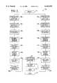
- first and second wafersare processed, with the processing blocks for the first wafer being identified in FIG. 1 with the suffix "a", and those to the second wafer designated with "b". Accordingly, only those steps for the first wafer will be described in detail, since those of skill in the art will readily appreciate similar steps may optionally also be performed in this embodiment on the second wafer also.
- a gettering layeris formed on the second side, side B, of the first wafer at Block 52a.
- the gettering layerwill be effective in removing contaminants, such as boron, for example, as will be readily appreciated by those skilled in the art.
- the gettering regionwill diffuse lifetime killing transition metals from the bulk of the wafer to the gettering site prior to thinning and direct bonding.
- typical gettering techniquesinclude phosphorous diffusion, ion implantations or argon or carbon, and/or polysilicon deposition on side B of the wafer.
- one or more active devicesmay be formed in a first side, i.e. side A, of the first wafer.
- the active devicesmay include one or more doped regions as may be formed by conventional techniques as will be readily appreciated by those skilled in the art.
- metal interconnectsmay also be formed, as described in greater detail below.
- the typical processing stepsmay include one or more of ion implantations, diffusions, metal depositions, polysilicon deposition, silicide formation, oxide growth, etc.
- the same or different types of MOSFET current controlled devicesmay be fabricated on the first and second substrates.
- the devices formed in accordance with the inventionare directed to having current conduction in a vertical direction, that is, perpendicular to the interface formed between the bonded together surfaces as will be readily appreciated by those skilled in the art.
- a vertical directionthat is, perpendicular to the interface formed between the bonded together surfaces
- the devicehas an N- base, then it would be desirable to inject a high density of holes (minority carriers) into the N- base to cause conductivity modulation.
- the condition for conductivity modulationis that the electron and hole densities in the base are equal.
- Conductivity modulationcauses the electron density to increase much beyond its equilibrium value and thereby lowers the resistance of the N- base significantly as will be readily appreciated by those skilled in the art.
- the first wafermay be secured to a handling wafer or support film (Block 56a) and at Block 58a, the first wafer is thinned on side B, thereby removing the gettering layer and the contaminants contained therein.
- the wafermay be thinned by grinding, for example, to reduce the thickness to less than about 200 nm, although even thinner wafers may be preferred for some applications.
- the handling wafer or support filmmay be removed after thinning.
- Side Bmay be polished and cleaned at Block 60a taking care to minimize hydrocarbon voids and to reduce oxygen at the ultimate bonding interface. If metal is exposed on the surface, such as metal bonding pads, it may be advantageous to protect the metal from chemicals used in the cleaning of the wafers.
- One possible techniqueis to deposit a protective insulator layer that is resistant to the chemicals. The insulator layer could be removed after the wafers are bonded.
- the polishingsuch as using chemical mechanical polishing (CMP), may be used so that the side B surface has a root-mean-square (RMS) surface roughness less than about 1 nm. A surface roughness of less than about 10 nm is desirable for direct bonding the two substrates together.
- CMPchemical mechanical polishing
- the bondingcould also be carried out at elevated temperatures of 200 to 400° C., for example, as will be readily appreciated by those skilled in the art.
- the cleaningis to remove hydrocarbons, organics, and metallic impurities from the surface.
- the cleaning processgenerally may use chemicals such as those used in RCA clean and piranha cleans as would be readily appreciated by those skilled in the art. Plasmas, UV, ozone, and laser irradiations may also be used to clean the surface prior to bonding.
- etchingmay be performed using a dilute hydrofluoric (HF) acid. It may also be desirable to minimize the native oxide regrowth prior to bonding.
- HFdilute hydrofluoric
- siliconone approach is to hydrogen terminate the silicon surface using a dilute HF etch followed by either no water rinse or minimal water rinse.
- Another more complicated approach to minimize native oxideis to direct bond the two wafers in either a vacuum, or in an ambient such as purified nitrogen, argon, or hydrogen that minimal concentrations of oxygen.
- Possible bond anneal ambientsinclude nitrogen, oxygen, argon, hydrogen.
- One possible mechanism by which the bond strength increases with anneal timeis that the hydrogen diffuses laterally along the bond interface and out of the wafer. The ambient may affect how readily the hydrogen diffuses laterally.
- the native oxidecan impede the current flow across the interface.
- the hydrophobic approachmay be susceptible to hydrocarbon absorption whereas a hydrophilic bonding approach in which there is a thin oxide at the interface may not be susceptible to hydrocarbon absorption.
- the oxide layermay be desirably less than about 1 nm for satisfactory operation.
- a side B of the first wafermay then optionally be implanted, such as for lifetime killing and/or with dopants for layers in the power device as will also be described in greater detail below.
- implantedsuch as for lifetime killing and/or with dopants for layers in the power device as will also be described in greater detail below.
- ion implantation of protons, helium, carbon, argon, oxygen, etc.may be used.
- Lifetime killing metalssuch as platinum or gold may also be implanted or diffused into the surface.
- the temperature required to diffuse the metalsmay be generally greater than about 450° C., therefore, it may not be possible to have aluminum on the back surface during the anneal.
- dopant layerslocated at or near the bonded interface of either or both of the wafers/substrates. Since all of the high temperature processing steps are performed on the wafers prior to thinning, relatively thin dopant layers at or near the bonding interface can be obtained by ion implantation or laser doping, since later high temperature steps are not needed. Such high temperature steps would diffuse the dopants in these thin regions. Laser annealing the implanted dopant may be performed to activate the dopants as will be readily appreciated by those skilled in the art.
- a photolithographic stepmay be used to define the location of the ion implanted dopant.
- the wafertypically includes a plurality of individual die thereon, these die can be tested (Block 64a) and the results later used to correlate with the second substrate to thereby increase the overall process yield.
- Yet another aspect of the inventionrelates to cutting the wafer along the outer streets (Block 66a). This will allow the precise alignment of the first and second wafers at Block 68.
- the wafersonce properly aligned, may be bonded by bringing same together at a center point and allowing atomic bonding to tend to bring the wafers together extending outwardly from the center. In some embodiments, a relatively high or ultrahigh vacuum may be desirable for the bonding process.
- the two wafersmay also be aligned based upon the crystal orientations of the two wafers as will also be appreciated by those skilled in the art.
- a low temperature annealmay be performed.
- the temperaturemay be less than about 800° C. if aluminum is to be added later, but may be 450° C. or less if the aluminum metal interconnects are already provided. If a barrier metal layer is provided between the aluminum and the silicon substrate a higher temperature anneal, e.g., about 450-550° C. may be permitted. Perhaps the best overall gains are achieved if the two wafers are completely processed prior to bonding.
- a significant requirement of the bond strengthis that it be strong enough for a 400° C. anneal to allow sawing or dicing. Accordingly, a bond interface energy of 800 ergs/cm 2 is required based on experience. A 400° C. anneal is potentially low enough to slow the formation of a Si--Al eutectic as will be appreciated by those skilled in the art. In other embodiments, laser cutting may be used so that a lower bond strength may be tolerated as will be appreciated by those skilled in the art.
- the individual device dies/circuitsmay be diced from the bonded together wafers using conventional techniques as will be readily appreciated by those skilled in the art.
- the power switching devices produced in accordance with the present inventionhave current transport across the bonding interface, that is, perpendicular to the bonding interface.
- the method of the present inventionallows the fabrication of double-sided MOSFET controlled power switching devices with a significant reduction in the number of sequential process steps by about a factor of two compared to conventional techniques.
- the direct bonding approachesallows current production recipes for fabricating single-side power devices to be used, and thus a separate process sequence does not need to be developed.
- the present inventionavoids the critical control of thermal budgets as in conventional processing, since an anneal is optimized for one dopant on the top side of the substrate but will not likely be optimized for another on the back side.
- the conventional approachmay also lead to yield losses from scratches, etc.
- the present inventionovercomes these drawbacks and also allows for a gettering operation to remove metal impurities prior to bonding.
- the yieldcan also be optimized by mapping the working die in the two wafers and aligning the wafers for best yield.
- the direct bonding after processing of the inventioncan be used to implement high performance IGBTs, MOSFETs, and MCTs, for example.
- the directed bonded devicesmay also have an ultra-thin N+ buffer layer which will provide significant improvements in the turn-off time compared to alternate approaches as described in greater detail below.
- the direct bonded IGBTs and MCTswill have a novel feature of positive temperature coefficient for forward voltage which arises from a negative temperature coefficient for current gain.
- a silicon MOSFET current control power devicein a first substrate to a second substrate that includes SiC material.
- Other candidates for the material of the second substratemay include GaN, InP, and GaAs.
- Wide bandgap materials, such as SiCgenerally have a high critical field of electrical breakdown, and also have high saturated drift velocities. Thus, wide bandgap materials are often desirable to be used to support most of the high voltage drop across depletion layers in power devices.
- Another reason for selecting a material for the second substrate to be different than siliconis to provide a high thermal conductivity.
- SiCwhich has a three times higher thermal conductivity than silicon may be used for the second substrate.
- two or more non-silicon substratesmay be processed and bonded in accordance with the present invention.
- one aspect of the present inventionis directed to an approach to achieve a double-sided MOSFET controlled power switching device using low temperature direct semiconductor--semiconductor wafer bonding by fabricating two MOSFET current control devices on two separate wafers, thinning the wafers from the backside to approximately 200 ⁇ m, and then performing aligned bonding of the wafers.
- the greatest advantage of this approachoccurs when the two wafers are almost completely processed prior to bonding.
- aluminum interconnectsare present on the surface and the maximum allowed bonding anneal temperature is about 450° C. If a barrier metal is used between the aluminum and silicon junction, bond anneal temperature of about 450-550° C. may be used.
- FIG. 2Initial processing of a first substrate 80 is shown in FIG. 2.
- the first substrate 80will be direct bonded to a second substrate 95 to produce a double-sided MCT 110 (FIG. 6) as will be appreciated by those skilled in the art.
- a gettering implant 91is provided as described in detail above.
- various dopant regionsare formed in the upper surface of the substrate 80, along with the illustrated second gate region 81.
- the illustrated processed portionfurther includes an N-type base 82, an N-type buffer layer 83 on the N-type base, and a P+ emitter 85 on the P-type base.
- the substrate 80also includes an anode layer 86 and an N+ region 87.
- the first substrate 80is joined to the handling substrate 90 or wafer, and the gettering layer 91 is removed by thinning to produce the intermediate structure shown in FIG. 4.
- a lifetime killing implant 92is schematically illustrated being formed in the first substrate 80 in FIG. 5.
- the thus processed first substrate 80is joined to a second substrate 95 after cleaning, direct bonding, and the low temperature anneal.
- the second substrate 95illustratively includes an N-type base 96, a P-type base 97 on the N-type base, an N+ emitter 98 on the N-type base, a first gate 99, a cathode layer 100, and the illustrated P+ region 101.
- the second substrate 95also illustratively includes the lifetime killing implants 102.
- An interface 103is schematically illustrated between the first and second substrates 80, 95.
- the first requirementis the need for near ideal current conduction across the bonding interface. This requires that there be minimal native oxide at the bonding interface. Prior researchers have demonstrated that by using hydrophobic bonding in which the silicon surfaces are hydrogen terminated, bonding interfaces with minimal native oxide can be obtained. Also special considerations should be given to reducing boron and heavy metal contamination during the surface cleaning operations. Another requirement is that bubbles and microvoids must be minimized at the bonding interface.
- Low temperature hydrophobically bonded wafersseem to be particularly susceptible to hydrocarbon generated voids, and thus special attention should also be paid to cleaning procedures that remove hydrocarbons. Yet another requirement is low minority carrier recombination at the bonding interface.
- FIGS. 7 through 12results from bonding experiments show that N-type to N-type and P-type to P-type silicon ⁇ 100> wafers can be hydrophobically bonded using low temperature anneals without producing potential barriers in either the conduction or valence bands.
- the cleaning procedure that was used to achieve a hydrogen terminated surfaceincluded combination of O 2 plasma and piranha cleans followed by a 10:1 HF dip, without a water rinse following the HF dip. Electrical data for the N-type to N-type wafers for various anneal temperatures is shown in FIG. 7.
- FIG. 8shows the resistance versus inverse area and a scatter plot of resistance values for N-type to N-type wafers annealed at 400° C. for 9 hours.
- FIG. 9shows a similar result for a P-type to P-type bond annealed at 400° C. for 24 hours.
- FIG. 10shows forward and reverse current-voltage characteristics for twenty diodes fabricated from hydrophobically bonded P-type to N-type wafers for a 600° C. bond anneal.
- the leakage current densityis approximately 40 nA/cm 2 despite the fact that the edges of the PN junction mesas were unpassivated, and which may be the lowest leakage current density obtained for hydrophobically bonded wafers.
- FIG. 11shows the calculated ideality factor for small forward biases for PN diodes with varying areas. The measurements show a strong dependence on area, with the smallest area diodes having the largest ideality factor values.
- FIG. 12shows that the bond strength increases logarithmically with anneal time, indicating a first order reaction for the bond kinetics at 400° C. A 400° C. anneal was chose because it is potentially low enough to slow the formation of Si--Al eutectic.
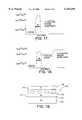
- a possible process to implement a low resistance metal or silicide strapped PN junctionis to use a photolithography step to define an implant of P-type dopant 121 into the N-type substrate 122 of the intermediate structure 120 shown in FIG. 13.
- a second photostepis used to define the location of the metal or silicide strip 123 within the P-type dopant region 121.
- the resist maskcan be used to etch about 100 nm of silicon.
- tungsten silicide 123about 30 nm of tungsten can be evaporated. The excess tungsten that is on the surface of the resist can be removed by lift-off, followed by an anneal to form tungsten silicide 123. As will be readily appreciated by those skilled in the art, an alternate approach may be to use a polishing technique to polish silicide that is formed above the silicon surface back planar with the adjacent silicon surface. The silicide can also be used to lower the resistance of a blanket doping layer, such as lowering the P-type base resistance of a Gate Turn-off Thyristor.
- a grid of low resistance PN junctionscan be used as gates of a vertical JFET 130.
- the pair of illustrated junctions 131, 132may be used to modulate a current flow perpendicular to the junctions, that is, across the interface 134.
- a plurality of such junctionscould also be formed.
- the depletion regions 135are formed around the P doped regions 123 as will be appreciated by those skilled in the art.
- MOS gatescould be formed on the sides of trenches and operate in the depletion mode in which the current is being conducted between the channels at zero source-to-gate bias, and the gate is biased to increase the depletion layer to turn off the device.
- a grid of silicide lines at the interface between the two substrates 125, 122can be used to form a permeable base transistor in which reverse biased Schottky diodes are used to modulate the current flow perpendicular to the grid of silicide lines 123 as will be readily appreciated by those skilled in the art.
- Viasmay be chemically or plasma etched from the top surface of either substrate to the silicide or metal layer using the silicide or metal layer as an etch stop layer.
- Another suitable techniquemay be to laser drill a via through the upper substrate 125 (FIG. 13), and stop at the metal or silicide layer.
- Yet another aspect of the inventionis the ability to epitaxially grow semiconductor layers on either or both of the substrates prior to bonding. If aluminum interconnects are on the substrates, the epitaxial growth should be at a temperature of less than 450° C., and less than 450 to 550° C. if a barrier metal layer is used as described above.
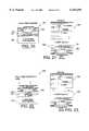
- the completed IGBT 140also includes an anode layer 142, a P+ substrate emitter layer 143 adjacent the anode, and the SiGe buffer layer 141 adjacent the interface 144.
- the upper substrate 150includes an external emitter layer 151, a gate layer 152 and its underlying insulator layer 153.
- the upper substrate 150also includes the N-type base 155 including the lifetime killing implant 156 as discussed above.
- the other doped regions of the upper substrate 150will be readily understood by those skilled in the art without further description.
- the SiGe base-emitter heterojunction that is properly configuredmay also have negative temperature coefficient for current gain, and, thus, positive temperature coefficient for forward voltage. This characteristic will provide short circuit protection and help prevent thermal run away as will be readily appreciated by those skilled in the art.
- the N+ buffer layermay be fabricated by implanting a thin, about 200 nm thick, layer with a concentration of about 1 ⁇ 10 19 cm -3 of N-type dopant, such as arsenic, antimony or phosphorous into the surface of the P+ substrate.
- the P+ substratemay have a concentration of about 3 ⁇ 10 18 to 1 ⁇ 10 19 cm -3 of P-type dopant.
- the substratecan then be annealed at a temperature of from about 900 to 1000° C. to anneal the defects created during ion implantation as would be readily appreciated by those skilled in the art.
- a techniques to prevent the injectionis to reduce the injection efficiency of holes in this region.
- a photolithography stepcan be performed to define a thick N+ ion implant into the regions outside of the active area to thereby reduce the injection efficiency.
- Other techniquescould also be used, such as to have a defined oxide barrier at the bonding interface 144.
- the thin epitaxial layers of SiGe or high N-type concentration dopantcan provide key advantages for the high performance IGBTs or MCTs.
- thin, high concentration dopant layerscan be used for the N+ buffer of an IGBT to achieve short turn-off time and negative temperature coefficient for current gain.
- the substratewas used as an N+ emitter, then the device would be processed to have a P+ ultra-thin buffer layer as will be readily appreciated by those skilled in the art.
- the device physics for a P+ emitter with an N+ base buffer layer that is higher in concentration than the P+ emitterresults in a negative temperature coefficient for current gain.
- the profilesare illustrated in FIG. 17 for the various portions of the device near the interface. The interface could be on either side of the N+ buffer as will be appreciated by those skilled in the art.
- the negative temperature coefficient for current gainimplies that the current in an IGBT or MCT decreases as the temperature increases. The current decreasing at higher temperatures means that the forward voltage will increase. Thus, the IGBT and MCT will have a positive temperature coefficient for forward voltage.
- a positive temperature coefficient for forward voltage for both IGBTs and MCTsis important to prevent thermal runaway and providing short circuit protection.
- the N+ buffer layerit is important to have an N+ buffer concentration that is higher than the P+ emitter; however, the N+ buffer must also be thin enough to provide sufficient current gain for the IGBT and MCT P+ backside emitters.
- the approach of using direct bonding or previously fabricated substrates that contain MOSFET current control deviceshas a particular advantage for making an IGBT or MCT with the N+ buffer concentration higher than the P+ substrate, and being relatively thin to produce acceptable current gain for the backside P+ emitter.
- a common approach used to presently make IGBTs or MCTsis to grow the N+ buffer using high temperature epitaxial growth. The high temperature epitaxial growth will diffuse the N+ dopant to make a thick buffer layer (10 to 20 ⁇ m thick). Because there is a maximum allowed N+ buffer integrated doping concentration, it is generally necessary that the N+ concentration be lower than the P+ substrate concentration to obtain backside P+ emitter current gain.
- high temperature (1100 to 1200° C.) annealsare typically used to diffuse P-type dopant to produce deep P-type junctions for field termination. If this high temperature process step is used after the N+ buffer is formed, this anneal will also diffuse the N-type dopant increasing the N+ buffer width. Since the integrated N+ buffer dopant (concentration integrated over thickness) must be low enough to provide sufficient gain for proper IGBT and MCT operation, a thicker N+ buffer must have a lower concentration. The high temperature field termination anneal thus makes it difficult to have an N+ buffer with a concentration greater than the P+ emitter concentration.
- a preferred approach to achieve an N+ buffer with a dopant concentration higher than the dopant concentration in the P+ emitteris to ion implant N-type ions (arsenic, phosphorous, antimony) into a P+ substrate that has a concentration of approximately 3 ⁇ 10 18 cm -3 . Because the ion implanted N-type dopant concentration is greater than the P+ doping concentration, the N-type dopant will over compensate the P+ doping concentration, and a thin, N+ layer can be formed on the pre-bonded surface of the substrate.
- the N+ buffer implantcan also be made into the prebonded surface of the other substrate. Since one of the substrates will have a thickness between 100 ⁇ m and 200 ⁇ m and may have metal interconnects on the surface thereof, it may generally be more difficult to perform the ion implant anneal.
- An alternate approach to make a thin N+ buffer with a concentration higher than the P+ emitteris to epitaxially grow the N+ buffer on the prebonded surface of either substrate before bonding.
- the P+ substrate concentrationis too high (such that a P+ to N+ junction would have too low of a breakdown voltage, have too much leakage current, or be too high concentration so that it is difficult to have an N+ buffer concentration greater than the P+ concentration) then an alternate approach is to first grow a lower concentration P-type epitaxial layer on the P+ substrate as understood with reference to FIG. 18. It is likely necessary to optimize the thickness and concentration of the P-type epitaxial layer. If the P-type epitaxial layer is thick enough (must be thicker than the diffusion length of electrons into the P+ emitter), then the doping concentration of the P-type epitaxial layer will determine the effective emitter concentration that determines the injection efficiency.
- the P-type epitaxial layermay be tens of microns thick and have a doping concentration of approximately 1 ⁇ 10 17 cm -3 .
- An approach for a thinner P-type epitaxial layeris to perform process steps to reduce the minority carrier lifetime in the P-type epitaxial layer.
- the diffusion length for electrons into the P-type emitteris determined by the recombination time for electrons in the P-type emitter.
- relatively low N+ buffer concentrationsare required to meet the criterion that the N+ buffer concentration be greater than the P+ emitter concentration.
- An N+ buffer ion implantcan now be made into the epitaxially grown P-type layer, or an N+ epitaxial layer grown on the P-type epitaxial layer growth. Direct bonding of the two substrates can now be performed.
- an alternate way to achieve negative temperature coefficient for current gainis to epitaxially grow a SiGe strained N+ buffer layer on the prebond surface of either substrate.
- Thin epitaxial layers of SiGe or high N-type concentration dopantcan provide key advantages for high performance IGBTs and MCTs.
- thin, high concentration dopant layerscan be used for the N+ buffer of an IGBT to achieve short turn-of time and negative temperature coefficient for current gain.
- thin layers of SiGecan act as the N+ buffer layer for an IGBT or MCT. Since the N+ buffer layer will be thin, the IGBT will have fast turn-off time.
- a SiGe base-emitter heterojunction that is properly designedalso has negative temperature coefficient for current gain and thus positive temperature coefficient for forward voltage. This characteristic will provide short circuit protection and help prevent thermal run away. If a first substrate is used as an N+ emitter, then the device would be processed to have a P+ buffer made into the second substrate.
- a first approachis an ultra-thinning approach, wherein the key requirement to achieve an N+ buffer concentration higher than P+ emitter concentration is to minimize temperature steps after the N+ buffer formation.
- a preferred fabrication approachis to:
- the maximum anneal temperatureis approximately 450 to 550° C. using conventional furnace annealing procedures. The 450 to 550° C. will only partially activate the boron and phosphorous implant dopants.
- a technique to achieve almost complete activation of the implanted boron and phosphorous ions even with metal interconnects present on the front surfaceis to use repetitive short pulses of excimer laser illumination.
- An alternate technique to implement an N+ buffer with a higher concentration than the P+ emitter on the back surface of the thinned substrateis to epitaxially grow the N+ buffer and P+ emitter on the back surface at approximately 500° C. If there are barrier metals under the aluminum interconnect, then growth temperatures of 500° C. are allowed.
- Molecular Beam Epitaxially (MBE) growth techniquesinclude Metal Organic Chemical Vapor Deposition (MOCVD) and Ultra-high Vacuum Chemical Vapor Deposition (UHVCVD).
- N+ and P+ amorphous silicon layersare also possible to deposit N+ and P+ amorphous silicon layers and then regrow the layer's single crystal layer at approximately 500° C. using solid phase epitaxial regrowth.
- An alternate technique to form a P+ emitter on the back surfaceis to use a P+ polysilicon layer. This type of emitter sometimes has a thin native oxide between the polysilicon layer and the single crystal layer that can provide an increase in current gain and in some cases, less change in current gain with temperature.
- High anneal temperaturescan be used to activate the ion implanted dopants on the back surface if metal interconnects are not present on the front surface in step 1 (in this case, the substrate is processed to just before metal deposition).
- the substrateis thinned, boron and phosphorous are implanted into the back surface, and an anneal at 800 to 900° C. is used to activate the implanted dopants. It will be necessary to perform the process steps and photolithography steps on the front surface to complete the process to make an IGBT. The difficult aspects of this process are that the wafer is approximately 100 ⁇ m thick at this point.
- the thinned IGBT or MCT substratecould be permanently bonded or soldered to a metal substrate, and the remaining processing steps completed.
- a technique for making a relatively narrow N+ buffer layeris to implant an N+ buffer into the prebond surface of a low N-type dopant concentration substrate, anneal the implant dopant, and then direct bond the substrate to a P+ emitter substrate. It is also possible to implant the N+ buffer dopant into the P+ substrate and over compensate the P+ dopant concentration.
- the N-type substrateis then thinned to approximately 100 ⁇ m and the diffusion and process steps to make an IGBT or MCT are next performed.
- the highest temperature stepis a 1100 to 1200° C. anneal to diffuse boron to make a deep junction for field termination. This high temperature step will cause the N+ buffer to diffuse and thus increase the thickness of the N+ buffer. With proper design and anneal temperature steps, it may be possible to produce an IGBT or MOSFET with the N+ buffer concentration higher than the P+ emitter concentration.
- One approach to achieve an N+ buffer concentration higher than the P+ emitter concentrationis to grow a relatively thick (10 ⁇ m) P-type epitaxial layer with a dopant concentration of approximately 1 ⁇ 10 17 cm -3 on the P+ substrate as illustrated in FIG. 18.
- the low concentration N-type substrate with the N+ buffer implanted into the prebond surfaceis then direct bonded to the P-type epitaxial surface.
- the effective dopant concentration for the P-type emitter injection efficiencywill be the P-type epitaxial layer dopant concentration rather than the P+ substrate dopant concentration.
- Yet another approach to achieve an N+ buffer concentration higher than the P+ emitter concentrationis to grow a relatively thick (10 ⁇ m-20 ⁇ m) P-type epitaxial layer with a dopant concentration of approximately 1 ⁇ 10 17 cm -3 on the P+ substrate as shown in FIG. 18. This epitaxial growth is followed by the epitaxial growth of an N+ buffer, and finally the epitaxial growth of the N- base layer. Since the epitaxial growth is a very high temperature process, it is difficult to achieve a thin N+ buffer and thus, it is difficult to achieve the condition that the N+ buffer concentration is greater than the P+ emitter concentration. The effective dopant concentration for the P-type emitter injection efficiency will be the P-type epitaxial layer dopant concentration rather than the P+ substrate dopant concentration.
- Another aspect of the inventionrelates to lateral localized lifetime killing near the direct bonded interface of IGBTs and MCTs.
- the device 170also is formed from an upper substrate 172 bonded to the lower substrate 171 at the schematically illustrated interface 173.
- the lower substrate 171illustratively includes an N+ doped portion 176 and an N doped portion 177.
- a photolithography stepor metal mesh would be used to define high energy proton (or other lifetime killing implants, defect generation techniques, or transition metal diffusions) so that they are laterally confined to certain regions.
- the region of the power device that has lifetime killing in ittypically has higher forward voltage since many of the injected carriers recombine in the lifetime killing region rather than transit from anode to cathode.
- By laterally confining the ion implanted lifetime killingthere will be regions of the device 170 that have no recombination of carriers as they transit from the anode to the cathode, and thus this portion of the device will have low (or ideal) forward voltage.
- the minority carriers that are in the base layertypically are removed from the base layer either by diffusing to the emitter-base junction or by diffusing to recombination centers.
- the lifetime killing implants 175are defined laterally, then the minority carriers in the base will diffuse laterally to the short lifetime recombination region. Since it is possible to photodefine resist that is approximately 10 ⁇ m thick to approximately 3 ⁇ m feature sizes, the lifetime killing region can consist of a grid of 2-3 ⁇ m diameter circular lifetime killing regions 175 that are buried approximately 10 ⁇ m from the prebond interface and are separated approximately every 10 ⁇ m laterally (parallel lines 2-3 ⁇ m wide separated every 10 ⁇ m is also an option).
- the effective distance the minority carriers then have to travel laterally to recombineis approximately 5 ⁇ m. Because of this short distance, the recombination time will be short. Thus, for the case that the lifetime killing is confined laterally, a high percentage of the injection PN junction area will not have lifetime killing, and an almost ideal turn-off time can be obtained while still achieving a fast turn-off time by having the minority carriers recombine laterally.
- the above described technique of laterally confining the lifetime killingalso has similar advantages for non-bonded devices such as PN diodes. It is desirable for a diode to have a low forward voltage so that it is desirable to have much of the diode area not have any lifetime killing. It is also desirable to have a fast turn-off time. Since much of the stored charge in a diode is near the PN junction, laterally confined lifetime killing regions (potentially implemented by high energy helium implant) that are approximately 4 ⁇ m to 8 ⁇ m into the N-type base from the PN junction are desirable.
- the lifetime killing regions that are spaced approximately 10 ⁇ m apart laterallywill provide a high percentage of the area that has no lifetime killing, but will yet provide fast turn-off time by allowing the carriers to diffuse laterally approximately 5 ⁇ m to recombine laterally. Lateral confined lifetime killing also has similar advantages for a thinned IGBT in which the P+ emitter anode is formed on the backside of an IGBT or MCT device structure on the cathode side.
- a common approach for fabricating a punchthrough IGBTis by epitaxially growing the N+ buffer and N- base layer on a P+ substrate. The processing steps for the diffusion and MOSFET control devices of the IGBT or MCT near the cathode are now performed. Because of the high temperature of the epitaxial layer growth (typically >1000° C.), lifetime killing, such as proton or HE implants or transition metal diffusion are typically performed after the epitaxial growth. There are several ion implantation lifetime killing techniques, however, than can remain as minority carrier recombination centers after the high temperature epitaxial growth.
- a key requirement for these lifetime killing techniquesis that the ion implantation to cause defects at the surface on which epitaxial layers will be grown so that good quality epitaxial layers can be grown.
- One techniqueis to implant He ions with sufficient energy so that they are buried beneath the surface about 0.5 ⁇ m and at sufficient doses (1 ⁇ 10 16 cm -3 ) so that when the substrate is heated, the He gas expands and creates bubbles beneath the silicon surface. These bubbles will survive the epitaxial layer growth. The silicon side walls of the bubbles can then act as precipitation centers for transition metals and as recombination centers for minority carriers.
- the approaches to localize the lifetime killing in the lateral directionis to use a photolightographically defined resist masking layer so that the He implants can define a grind of 2-3 ⁇ m diameter circular lifetime killing regions that are buried about 0.5 ⁇ m beneath the surface on which the epitaxial layer will be grown and are separated about every 10 to 20 ⁇ m laterally. Parallel lines 2-3 ⁇ m wide may be separated every 10-20 ⁇ m as an option.
- the process for forming and growing the epitaxial layer and lateral lifetime killingis thus:
- an epitaxial layerincluding about a 10 ⁇ m thick N+ buffer and a 10 ⁇ m N- base layer on a P+ substrate.
- ion implantation lifetime killing speciesthat can be used in a similar manner on the He implant described above are:
- a. oxygen implantto create oxygen precipitates that are buried beneath the silicon surface that will act as recombination centers.
- the anneal to create oxygen precipitatestypically involves a long time anneal at 650° C. to nucleate the precipitates, an anneal at 950° C. to grow the precipitates, and then possibly an anneal at 1100° C. to grow stacking faults.
- the ion implantation dose typically required to create a high density of oxygenis typically less than about 1 ⁇ 10 15 cm -3 and will not roughen the surface as much as is the case for the He implant that causes the bubbles.
- a non-laterally localized killing region of the pre-epitaxial growth lifetime killingmay be desirable.
- the following descriptionrelates to alternate approaches to implement: 1) an N+ buffer near the P-type body on the anode side of the device, 2) a positive temperature coefficient for forward voltage for a double-side power device, 3) the use of a silicon-on-insulator (SOI) substrate to form thin anode side and cathode side devices that need not be polished prior to bonding, and 4) electrochemical etching to form thin power device layers.
- SOIsilicon-on-insulator
- a number of power switching applicationsonly require forward blocking operation and do not require reverse blocking operation.
- active device structure and field terminationare required on the cathode side of the device to achieve high breakdown voltage, however, only a low breakdown voltage device is required on the anode side of the device.
- the principle methods for implementing an N+ buffer in a double-sided deviceinclude those described herein for direct bonding after the substrates have been processed. There are several methods which are also appropriate to implementing a power switching device which is fabricated using conventional double-sided semiconductor processing.
- Epitaxial growthmay be used on the anode side substrate prior to fabrication of the anode side active devices.
- an epitaxial layer including an N- base layer 182 and an N+ buffer layer 181 and finally a lower doped N layeris grown on a float zone N-type substrate 183 as shown in FIG. 20.
- a two doping concentration buffermay be desired for robustness.
- the two doping concentration bufferwould include the epitaxial growth of a wide, lower doping concentration N-type buffer and then a thin N+ buffer.
- the N+ buffer layerwill generally be located about 2 ⁇ m to 20 ⁇ m from the top surface.
- the MOSFET current control devices located on the anode side of the devicecan then be fabricated within the P-type body 185 as illustrated.
- the P bodywill also form the emitter of a PNP bipolar transistor consisting of the P-type body emitter, N+ buffer/N-type base, and P-type collector on the cathode side of the device.
- the direct bond approach used to fabricate a double-sided power device including the above described N+ bufferis to fabricate the anode side substrate as described above, thin to about 10 ⁇ m to 200 ⁇ m, polish and clean the surface, hydrogen terminate the surface, and then direct bond to a thinned and polished cathode side substrate 190 as shown in FIG. 21.
- the direct bond approachcan readily form the two-step N buffer as described above by having the N-type substrate concentration of the anode side substrate 180 be the desired concentration of the lower concentration N-type buffer of the two step N-type buffer.
- a double-sided power device with an N+ buffer near the anode side current control devicecan be fabricated by epitaxial growth as described above, but with the double-sided semiconductor processing instead of the direct wafer bond technique.
- a high energy implant of phosphorousmay be used to form the N+ buffer region 181' of the substrate 180' as shown in FIG. 22.
- the other portions of the substrate 180'are the same as those described above for FIGS. 20 and 21, and need no further discussion herein.
- FIG. 23further illustrates the bonding of the two substrates 190, 180' and needs no further description.
- a positive temperature coefficient for forward voltage for a double-sided power devicecan be obtained by having an N+ buffer concentration greater than the P-type body emitter concentration as described above.
- the N+ buffer layeris formed on the N- base float zone substrate portion 203.
- FIG. 25illustrates the direct bonding of the thus formed anode side substrate 200 to the illustrated cathode side substrate 210.
- An alternate approach to implement an N+ bufferis to use silicon-on-insulator (SOI) technology.
- SOIsilicon-on-insulator
- an N+ ion implant to form the N+ buffer 221is made into one surface of a the anode side substrate 220 as shown in the top portion of FIG. 26.
- This substrate 220will later be bonded to the silicon substrate 227 with oxide 226 on the surface thereof to form the SOI substrate 225 as shown in the lower portion of FIG. 26.
- the active device portion of the anode side substrate 220is next fabricated as seen in the upper portion of FIG. 26.
- the silicon substrate and SOI layerPrior to direct bonding to form the double-sided power device, the silicon substrate and SOI layer are removed by protecting the front surface of the wafer, grinding to within 50 ⁇ m of the oxide layer, chemically etching the silicon and stopping the etch at the oxide layer, and finally chemically etching the oxide layer.
- An advantage of the SOI substrateis that the surface roughness should be sufficiently small so that a polishing operation is not required.
- the previously fabricated anode side substrate 220can be direct bonded to the previously fabricated cathode side substrate 230 as shown in FIG. 27.
- An ion implanted N+ buffermay be formed into the prebond surface of an ultra-thin previously fabricated anode side substrate.
- an N+ ion implantis made into one of the prebond surface of either the anode side or cathode side substrate. It is generally desirable that the anode side substrate be about 3 ⁇ m to 20 ⁇ m thick to form the N+ buffer near the P-body.
- the ultra-thin anode side substratecan be implemented by the SOI approach described immediately above, grinding, and polishing, hydrogen ion implant layer splitting, and electrochemical etchstop plus polishing.
- a thin anode side substratecan be formed by epitaxially growing an N-type base layer, N+ buffer, N-type base layer on a P-type substrate and forming an anode side active device as described above.
- the electrochemical etch stop approachtypically the P-type substrate is etched with the etch stopping within the PN junction depletion layer.
- thin active side substratescan be formed. It is generally necessary that the surface be polished to obtain a small enough surface roughness to direct bond to the cathode side substrate.
- the electrochemical etch stop techniquerequires a method to make electrical contact to the front side of the device while at the same time protecting the front side of the wafer.
- a potential approachis to perform both functions by using a conductive polymer.
- Another SOI approach to fabricate thin substrates for direct bonding to form a double-sided power deviceis to fabricate one or both sides of a double-sided power device in the top silicon layer of an SOI substrate, remove the substrate and oxide, and direct bond two previously fabricated substrates to form the device.
- the primary advantage of this approachis that it is not necessary to polish the prebond surface prior to direct bonding.
- the SOI approach to direct bonded double-sided power devicesis useful whether or not an N+ buffer is included and is even useful if only forming a one sided IGBT or MCT device.
- the typical processis to direct bond an oxidized surface of small surface roughness ( ⁇ 1 nm), and prime the surface finish of the silicon wafer to a silicon handle substrate.
- the silicon surface that is adjacent the buried oxide layerhas a small surface roughness.
- the approach to use an SOI substrate to form a double-sided power deviceis then to polish the top silicon layer to the desired thickness generally in the range of about 3 to 100 ⁇ m thickness, fabricate the power switching device in the top silicon layer, remove the silicon handle substrate, remove the oxide layer, potentially ion implant into the prebond surface, and then direct bond two previously fabricated substrates to form a double-sided power switching device.
- This processmay be better understood with reference to FIGS. 28 and 29.
- the anode side substrate 230is bonded to the SOI substrate 240, and in FIG. 29, afer the SOI substrate is removed, the anode side substrate 230 is joined to the cathode side substrate 250.
- some high voltage power devicesmay require a silicon substrate thickness of 2 mm. This is a relatively thick substrate that can be formed by bonding together four 0.5 mm thick substrates, and with the top and bottom substrates having the processing already performed prior to bonding in accordance with the invention.
- MOSFET control deviceson one or both of the wafer surfaces
- inventive principles and techniquesalso apply to non-MOSFET current control devices, such as Gate Turn-off Thyristors, thyristors, bipolar transistors and diodes.
- wafer and substratehave been used interchangeably herein, and that each are intended to cover single as well as multiple devices.
Landscapes
- Engineering & Computer Science (AREA)
- Physics & Mathematics (AREA)
- Condensed Matter Physics & Semiconductors (AREA)
- General Physics & Mathematics (AREA)
- Manufacturing & Machinery (AREA)
- Computer Hardware Design (AREA)
- Microelectronics & Electronic Packaging (AREA)
- Power Engineering (AREA)
- Electrodes Of Semiconductors (AREA)
Abstract
Description
(EIE)=J.sub.e /J.sub.h,
J.sub.e =(qR.sub.ip.sup.2 D.sub.p /N.sub.A W.sub.P)e.sup.qv/kT ;
J.sub.h =qR.sub.in.sup.2 D.sub.n /N.sub.D W.sub.e
Claims (83)
Priority Applications (5)
| Application Number | Priority Date | Filing Date | Title |
|---|---|---|---|
| US09/036,815US6153495A (en) | 1998-03-09 | 1998-03-09 | Advanced methods for making semiconductor devices by low temperature direct bonding |
| EP99912328AEP1062692A1 (en) | 1998-03-09 | 1999-03-09 | Devices formable by low temperature direct bonding |
| KR1020007010106AKR20010041822A (en) | 1998-03-09 | 1999-03-09 | Devices formable by low temperature direct bonding |
| JP2000536101AJP2002507058A (en) | 1998-03-09 | 1999-03-09 | Equipment that can be formed by low-temperature direct bonding |
| PCT/US1999/005066WO1999046809A1 (en) | 1998-03-09 | 1999-03-09 | Devices formable by low temperature direct bonding |
Applications Claiming Priority (1)
| Application Number | Priority Date | Filing Date | Title |
|---|---|---|---|
| US09/036,815US6153495A (en) | 1998-03-09 | 1998-03-09 | Advanced methods for making semiconductor devices by low temperature direct bonding |
Publications (1)
| Publication Number | Publication Date |
|---|---|
| US6153495Atrue US6153495A (en) | 2000-11-28 |
Family
ID=21890806
Family Applications (1)
| Application Number | Title | Priority Date | Filing Date |
|---|---|---|---|
| US09/036,815Expired - LifetimeUS6153495A (en) | 1998-03-09 | 1998-03-09 | Advanced methods for making semiconductor devices by low temperature direct bonding |
Country Status (1)
| Country | Link |
|---|---|
| US (1) | US6153495A (en) |
Cited By (338)
| Publication number | Priority date | Publication date | Assignee | Title |
|---|---|---|---|---|
| WO2001061743A1 (en)* | 2000-02-16 | 2001-08-23 | Ziptronix, Inc. | Method for low temperature bonding and bonded structure |
| US6410371B1 (en) | 2001-02-26 | 2002-06-25 | Advanced Micro Devices, Inc. | Method of fabrication of semiconductor-on-insulator (SOI) wafer having a Si/SiGe/Si active layer |
| US6444493B1 (en)* | 1998-12-08 | 2002-09-03 | Fraunhofer-Gesellschaft Zur Foerderung Der Angewandten Forschung E.V. | Method for vertically integrating active circuit planes and vertically integrated circuit produced using said method |
| US6455398B1 (en)* | 1999-07-16 | 2002-09-24 | Massachusetts Institute Of Technology | Silicon on III-V semiconductor bonding for monolithic optoelectronic integration |
| US20030034529A1 (en)* | 2000-12-04 | 2003-02-20 | Amberwave Systems Corporation | CMOS inverter and integrated circuits utilizing strained silicon surface channel MOSFETs |
| US6548420B2 (en)* | 2001-01-26 | 2003-04-15 | International Business Machines Corporation | Measurement and analysis of mercury-based pseudo-field effect transistors |
| US20030079503A1 (en)* | 2001-10-26 | 2003-05-01 | Cook Glen B. | Direct bonding of glass articles for drawing |
| US20030081906A1 (en)* | 2001-10-26 | 2003-05-01 | Filhaber John F. | Direct bonding of optical components |
| US20030079823A1 (en)* | 2001-10-26 | 2003-05-01 | Robert Sabia | Direct bonding of articles containing silicon |
| US6573126B2 (en) | 2000-08-16 | 2003-06-03 | Massachusetts Institute Of Technology | Process for producing semiconductor article using graded epitaxial growth |
| US6602613B1 (en) | 2000-01-20 | 2003-08-05 | Amberwave Systems Corporation | Heterointegration of materials using deposition and bonding |
| US20030164006A1 (en)* | 2001-10-26 | 2003-09-04 | Buchanan Karl H. | Direct bonding of glass articles for drawing |
| US20030188553A1 (en)* | 2002-04-08 | 2003-10-09 | Mann Larry G. | Direct bonding methods using lithium |
| US20030206347A1 (en)* | 2002-05-02 | 2003-11-06 | Robert Sabia | Optical isolators and methods of manufacture |
| US6649480B2 (en) | 2000-12-04 | 2003-11-18 | Amberwave Systems Corporation | Method of fabricating CMOS inverter and integrated circuits utilizing strained silicon surface channel MOSFETs |
| US20030230113A1 (en)* | 2002-06-12 | 2003-12-18 | Patrick Gedeon | Methods for manufacturing glass articles |
| US6677173B2 (en)* | 2000-03-28 | 2004-01-13 | Pioneer Corporation | Method of manufacturing a nitride semiconductor laser with a plated auxiliary metal substrate |
| US6703688B1 (en) | 2001-03-02 | 2004-03-09 | Amberwave Systems Corporation | Relaxed silicon germanium platform for high speed CMOS electronics and high speed analog circuits |
| US6724008B2 (en) | 2001-03-02 | 2004-04-20 | Amberwave Systems Corporation | Relaxed silicon germanium platform for high speed CMOS electronics and high speed analog circuits |
| US6723661B2 (en) | 2001-03-02 | 2004-04-20 | Amberwave Systems Corporation | Relaxed silicon germanium platform for high speed CMOS electronics and high speed analog circuits |
| US20040087110A1 (en)* | 2002-07-16 | 2004-05-06 | Semiconductor Energy Laboratory Co., Ltd. | Peeling method |
| US20040092084A1 (en)* | 2002-10-30 | 2004-05-13 | Olivier Rayssac | Method for treating a semiconductor material for subsequent bonding |
| US6750130B1 (en) | 2000-01-20 | 2004-06-15 | Amberwave Systems Corporation | Heterointegration of materials using deposition and bonding |
| US20040132265A1 (en)* | 2002-12-27 | 2004-07-08 | Semiconductor Energy Laboratory Co., Ltd. | Separating method |
| US20040150087A1 (en)* | 2002-11-20 | 2004-08-05 | Hyogo Prefecture | Method for removing impurities of a semiconductor wafer, semiconductor wafer assembly, and semiconductor device |
| US20040174598A1 (en)* | 2003-01-29 | 2004-09-09 | Kyocera Corporation | Optical isolator element, a method for producing such an element, and an optical isolator using such an element |
| US6791748B2 (en) | 2002-05-02 | 2004-09-14 | Corning Incorporated | Optical isolators and methods of manufacture |
| US20040226910A1 (en)* | 2002-12-30 | 2004-11-18 | Chatterjee Dilip K. | Bulk optical elements incorporating gratings for optical communications and methods for producing |
| US6836602B2 (en) | 2001-10-26 | 2004-12-28 | Corning Incorporated | Direct bonding of optical components |
| US6864585B2 (en) | 2000-03-22 | 2005-03-08 | Ziptronix, Inc. | Three dimensional device integration method and integrated device |
| US6864115B2 (en) | 2000-01-20 | 2005-03-08 | Amberwave Systems Corporation | Low threading dislocation density relaxed mismatched epilayers without high temperature growth |
| US6876010B1 (en) | 1997-06-24 | 2005-04-05 | Massachusetts Institute Of Technology | Controlling threading dislocation densities in Ge on Si using graded GeSi layers and planarization |
| US6881994B2 (en)* | 2000-08-14 | 2005-04-19 | Matrix Semiconductor, Inc. | Monolithic three dimensional array of charge storage devices containing a planarized surface |
| US6890835B1 (en)* | 2000-10-19 | 2005-05-10 | International Business Machines Corporation | Layer transfer of low defect SiGe using an etch-back process |
| US6933518B2 (en) | 2001-09-24 | 2005-08-23 | Amberwave Systems Corporation | RF circuits including transistors having strained material layers |
| US6940089B2 (en) | 2001-04-04 | 2005-09-06 | Massachusetts Institute Of Technology | Semiconductor device structure |
| US20050280154A1 (en)* | 2004-06-21 | 2005-12-22 | Sang-Yun Lee | Semiconductor memory device |
| US20050280042A1 (en)* | 2004-06-21 | 2005-12-22 | Sang-Yun Lee | Wafer bonding method |
| US20050280155A1 (en)* | 2004-06-21 | 2005-12-22 | Sang-Yun Lee | Semiconductor bonding and layer transfer method |
| US6984571B1 (en) | 1999-10-01 | 2006-01-10 | Ziptronix, Inc. | Three dimensional device integration method and integrated device |
| US6995430B2 (en) | 2002-06-07 | 2006-02-07 | Amberwave Systems Corporation | Strained-semiconductor-on-insulator device structures |
| US20060030121A1 (en)* | 2004-08-09 | 2006-02-09 | Micron Technology, Inc. | Epitaxial semiconductor layer and method |
| US7049627B2 (en) | 2002-08-23 | 2006-05-23 | Amberwave Systems Corporation | Semiconductor heterostructures and related methods |
| US20060113603A1 (en)* | 2004-12-01 | 2006-06-01 | Amberwave Systems Corporation | Hybrid semiconductor-on-insulator structures and related methods |
| US20060118728A1 (en)* | 2004-12-03 | 2006-06-08 | Bernard Phlips | Wafer bonded silicon radiation detectors |
| US7060632B2 (en) | 2002-03-14 | 2006-06-13 | Amberwave Systems Corporation | Methods for fabricating strained layers on semiconductor substrates |
| US7074623B2 (en) | 2002-06-07 | 2006-07-11 | Amberwave Systems Corporation | Methods of forming strained-semiconductor-on-insulator finFET device structures |
| US7122449B2 (en) | 2002-06-10 | 2006-10-17 | Amberwave Systems Corporation | Methods of fabricating semiconductor structures having epitaxially grown source and drain elements |
| US20070085160A1 (en)* | 2004-07-08 | 2007-04-19 | International Rectifier Corporation | Process for resurf diffusion for high voltage MOSFET |
| US7217603B2 (en) | 2002-06-25 | 2007-05-15 | Amberwave Systems Corporation | Methods of forming reacted conductive gate electrodes |
| US7227176B2 (en) | 1998-04-10 | 2007-06-05 | Massachusetts Institute Of Technology | Etch stop layer system |
| US7250646B2 (en) | 2001-08-13 | 2007-07-31 | Sandisk 3D, Llc. | TFT mask ROM and method for making same |
| US20070193682A1 (en)* | 2004-04-08 | 2007-08-23 | Matsushita Electric Industrial Co., Ltd. | Bonding method and apparatus |
| US7307273B2 (en) | 2002-06-07 | 2007-12-11 | Amberwave Systems Corporation | Control of strain in device layers by selective relaxation |
| US20070284730A1 (en)* | 2006-06-12 | 2007-12-13 | Wei Shi | Method, apparatus, and system for thin die thin thermal interface material in integrated circuit packages |
| US20080014439A1 (en)* | 2006-03-25 | 2008-01-17 | Igor Bol | Process for manufacture of thin wafer |
| US20080020541A1 (en)* | 2006-07-24 | 2008-01-24 | Yasunobu Ikeda | Method for manufacturing bonded SOI wafer and bonded SOI wafer manufactured thereby |
| US7332410B2 (en) | 2000-08-09 | 2008-02-19 | Ziptronix, Inc. | Method of epitaxial-like wafer bonding at low temperature and bonded structure |
| US7332417B2 (en) | 2003-01-27 | 2008-02-19 | Amberwave Systems Corporation | Semiconductor structures with structural homogeneity |
| US7335545B2 (en) | 2002-06-07 | 2008-02-26 | Amberwave Systems Corporation | Control of strain in device layers by prevention of relaxation |
| US20080048327A1 (en)* | 2004-06-21 | 2008-02-28 | Sang-Yun Lee | Electronic circuit with embedded memory |
| US7393733B2 (en) | 2004-12-01 | 2008-07-01 | Amberwave Systems Corporation | Methods of forming hybrid fin field-effect transistor structures |
| US20080191312A1 (en)* | 2003-06-24 | 2008-08-14 | Oh Choonsik | Semiconductor circuit |
| US20080274413A1 (en)* | 2007-03-22 | 2008-11-06 | Micron Technology, Inc. | Sub-10 nm line features via rapid graphoepitaxial self-assembly of amphiphilic monolayers |
| US7504704B2 (en) | 2003-03-07 | 2009-03-17 | Amberwave Systems Corporation | Shallow trench isolation process |
| US20090111241A1 (en)* | 2003-06-24 | 2009-04-30 | Sang-Yun Lee | Wafer bonding method |
| US20090224364A1 (en)* | 2003-06-24 | 2009-09-10 | Oh Choonsik | Semiconductor circuit and method of fabricating the same |
| US7594967B2 (en) | 2002-08-30 | 2009-09-29 | Amberwave Systems Corporation | Reduction of dislocation pile-up formation during relaxed lattice-mismatched epitaxy |
| US7615829B2 (en) | 2002-06-07 | 2009-11-10 | Amberwave Systems Corporation | Elevated source and drain elements for strained-channel heterojuntion field-effect transistors |
| US20090325343A1 (en)* | 2003-06-24 | 2009-12-31 | Sang-Yun Lee | Bonded semiconductor structure and method of fabricating the same |
| US20100038743A1 (en)* | 2003-06-24 | 2010-02-18 | Sang-Yun Lee | Information storage system which includes a bonded semiconductor structure |
| US20100108970A1 (en)* | 2008-10-30 | 2010-05-06 | Jun Liu | Memory Devices and Formation Methods |
| US7723209B2 (en) | 2002-12-27 | 2010-05-25 | Semiconductor Energy Laboratory Co., Ltd. | Semiconductor device and manufacturing method thereof, delamination method, and transferring method |
| US20100133695A1 (en)* | 2003-01-12 | 2010-06-03 | Sang-Yun Lee | Electronic circuit with embedded memory |
| US20100190334A1 (en)* | 2003-06-24 | 2010-07-29 | Sang-Yun Lee | Three-dimensional semiconductor structure and method of manufacturing the same |
| US7776697B2 (en) | 2001-09-21 | 2010-08-17 | Taiwan Semiconductor Manufacturing Company, Ltd. | Semiconductor structures employing strained material layers with defined impurity gradients and methods for fabricating same |
| US20100316849A1 (en)* | 2008-02-05 | 2010-12-16 | Millward Dan B | Method to Produce Nanometer-Sized Features with Directed Assembly of Block Copolymers |
| US20110003438A1 (en)* | 2005-03-29 | 2011-01-06 | Sang-Yun Lee | Three-dimensional integrated circuit structure |
| US7867822B2 (en) | 2003-06-24 | 2011-01-11 | Sang-Yun Lee | Semiconductor memory device |
| US20110053332A1 (en)* | 2003-06-24 | 2011-03-03 | Sang-Yun Lee | Semiconductor circuit |
| US20110143506A1 (en)* | 2009-12-10 | 2011-06-16 | Sang-Yun Lee | Method for fabricating a semiconductor memory device |
| US20110212595A1 (en)* | 2010-02-26 | 2011-09-01 | Jerry Hu | Semiconductor device structure and methods of making |
| US20110232515A1 (en)* | 2007-04-18 | 2011-09-29 | Micron Technology, Inc. | Methods of forming a stamp, a stamp and a patterning system |
| US8058142B2 (en) | 1996-11-04 | 2011-11-15 | Besang Inc. | Bonded semiconductor structure and method of making the same |
| US20120104415A1 (en)* | 2010-10-27 | 2012-05-03 | Mitsubishi Electronic Corporation | Semiconductor device |
| US8203148B2 (en) | 2010-10-11 | 2012-06-19 | Monolithic 3D Inc. | Semiconductor device and structure |
| US20120153438A1 (en)* | 2010-12-16 | 2012-06-21 | Solid State Devices, Inc. | Multiple noble metals for lifetime suppression for power semiconductors |
| US8237228B2 (en) | 2009-10-12 | 2012-08-07 | Monolithic 3D Inc. | System comprising a semiconductor device and structure |
| US8273610B2 (en) | 2010-11-18 | 2012-09-25 | Monolithic 3D Inc. | Method of constructing a semiconductor device and structure |
| US8294159B2 (en) | 2009-10-12 | 2012-10-23 | Monolithic 3D Inc. | Method for fabrication of a semiconductor device and structure |
| US8362482B2 (en) | 2009-04-14 | 2013-01-29 | Monolithic 3D Inc. | Semiconductor device and structure |
| US8362800B2 (en) | 2010-10-13 | 2013-01-29 | Monolithic 3D Inc. | 3D semiconductor device including field repairable logics |
| US8373439B2 (en) | 2009-04-14 | 2013-02-12 | Monolithic 3D Inc. | 3D semiconductor device |
| US8373230B1 (en) | 2010-10-13 | 2013-02-12 | Monolithic 3D Inc. | Method for fabrication of a semiconductor device and structure |
| US8378494B2 (en) | 2009-04-14 | 2013-02-19 | Monolithic 3D Inc. | Method for fabrication of a semiconductor device and structure |
| US8379458B1 (en) | 2010-10-13 | 2013-02-19 | Monolithic 3D Inc. | Semiconductor device and structure |
| US8378715B2 (en) | 2009-04-14 | 2013-02-19 | Monolithic 3D Inc. | Method to construct systems |
| US8384426B2 (en) | 2009-04-14 | 2013-02-26 | Monolithic 3D Inc. | Semiconductor device and structure |
| US8405420B2 (en) | 2009-04-14 | 2013-03-26 | Monolithic 3D Inc. | System comprising a semiconductor device and structure |
| US8427200B2 (en) | 2009-04-14 | 2013-04-23 | Monolithic 3D Inc. | 3D semiconductor device |
| US8440542B2 (en) | 2010-10-11 | 2013-05-14 | Monolithic 3D Inc. | Semiconductor device and structure |
| US8450804B2 (en) | 2011-03-06 | 2013-05-28 | Monolithic 3D Inc. | Semiconductor device and structure for heat removal |
| US8455978B2 (en) | 2010-05-27 | 2013-06-04 | Sang-Yun Lee | Semiconductor circuit structure and method of making the same |
| US8461035B1 (en) | 2010-09-30 | 2013-06-11 | Monolithic 3D Inc. | Method for fabrication of a semiconductor device and structure |
| US8476145B2 (en) | 2010-10-13 | 2013-07-02 | Monolithic 3D Inc. | Method of fabricating a semiconductor device and structure |
| US8492886B2 (en) | 2010-02-16 | 2013-07-23 | Monolithic 3D Inc | 3D integrated circuit with logic |
| US8536023B2 (en) | 2010-11-22 | 2013-09-17 | Monolithic 3D Inc. | Method of manufacturing a semiconductor device and structure |
| US8541819B1 (en) | 2010-12-09 | 2013-09-24 | Monolithic 3D Inc. | Semiconductor device and structure |
| US8557632B1 (en) | 2012-04-09 | 2013-10-15 | Monolithic 3D Inc. | Method for fabrication of a semiconductor device and structure |
| US8574929B1 (en) | 2012-11-16 | 2013-11-05 | Monolithic 3D Inc. | Method to form a 3D semiconductor device and structure |
| US8581349B1 (en) | 2011-05-02 | 2013-11-12 | Monolithic 3D Inc. | 3D memory semiconductor device and structure |
| US8609221B2 (en) | 2007-06-12 | 2013-12-17 | Micron Technology, Inc. | Alternating self-assembling morphologies of diblock copolymers controlled by variations in surfaces |
| US8633112B2 (en) | 2008-03-21 | 2014-01-21 | Micron Technology, Inc. | Thermal anneal of block copolymer films with top interface constrained to wet both blocks with equal preference |
| US8641914B2 (en) | 2008-03-21 | 2014-02-04 | Micron Technology, Inc. | Methods of improving long range order in self-assembly of block copolymer films with ionic liquids |
| US8642416B2 (en) | 2010-07-30 | 2014-02-04 | Monolithic 3D Inc. | Method of forming three dimensional integrated circuit devices using layer transfer technique |
| US8669645B2 (en) | 2008-10-28 | 2014-03-11 | Micron Technology, Inc. | Semiconductor structures including polymer material permeated with metal oxide |
| US8669778B1 (en) | 2009-04-14 | 2014-03-11 | Monolithic 3D Inc. | Method for design and manufacturing of a 3D semiconductor device |
| US20140070267A1 (en)* | 2012-09-13 | 2014-03-13 | Magnachip Semiconductor, Ltd. | Power semiconductor device and fabrication method thereof |
| US8674470B1 (en) | 2012-12-22 | 2014-03-18 | Monolithic 3D Inc. | Semiconductor device and structure |
| US8687399B2 (en) | 2011-10-02 | 2014-04-01 | Monolithic 3D Inc. | Semiconductor device and structure |
| US8686428B1 (en) | 2012-11-16 | 2014-04-01 | Monolithic 3D Inc. | Semiconductor device and structure |
| US8709880B2 (en) | 2010-07-30 | 2014-04-29 | Monolithic 3D Inc | Method for fabrication of a semiconductor device and structure |
| US8723335B2 (en) | 2010-05-20 | 2014-05-13 | Sang-Yun Lee | Semiconductor circuit structure and method of forming the same using a capping layer |
| US8742476B1 (en) | 2012-11-27 | 2014-06-03 | Monolithic 3D Inc. | Semiconductor device and structure |
| US8748292B2 (en) | 2002-06-07 | 2014-06-10 | Taiwan Semiconductor Manufacturing Company, Ltd. | Methods of forming strained-semiconductor-on-insulator device structures |
| US8753913B2 (en) | 2010-10-13 | 2014-06-17 | Monolithic 3D Inc. | Method for fabricating novel semiconductor and optoelectronic devices |
| US8754533B2 (en) | 2009-04-14 | 2014-06-17 | Monolithic 3D Inc. | Monolithic three-dimensional semiconductor device and structure |
| US8753738B2 (en) | 2007-03-06 | 2014-06-17 | Micron Technology, Inc. | Registered structure formation via the application of directed thermal energy to diblock copolymer films |
| US8785559B2 (en) | 2007-06-19 | 2014-07-22 | Micron Technology, Inc. | Crosslinkable graft polymer non-preferentially wetted by polystyrene and polyethylene oxide |
| US8803206B1 (en) | 2012-12-29 | 2014-08-12 | Monolithic 3D Inc. | 3D semiconductor device and structure |
| US8822282B2 (en) | 2001-03-02 | 2014-09-02 | Taiwan Semiconductor Manufacturing Company, Ltd. | Methods of fabricating contact regions for FET incorporating SiGe |
| US8902663B1 (en) | 2013-03-11 | 2014-12-02 | Monolithic 3D Inc. | Method of maintaining a memory state |
| US8901613B2 (en) | 2011-03-06 | 2014-12-02 | Monolithic 3D Inc. | Semiconductor device and structure for heat removal |
| US8900963B2 (en) | 2011-11-02 | 2014-12-02 | Micron Technology, Inc. | Methods of forming semiconductor device structures, and related structures |
| US8975670B2 (en) | 2011-03-06 | 2015-03-10 | Monolithic 3D Inc. | Semiconductor device and structure for heat removal |
| US8993088B2 (en) | 2008-05-02 | 2015-03-31 | Micron Technology, Inc. | Polymeric materials in self-assembled arrays and semiconductor structures comprising polymeric materials |
| US8994404B1 (en) | 2013-03-12 | 2015-03-31 | Monolithic 3D Inc. | Semiconductor device and structure |
| US9000557B2 (en) | 2012-03-17 | 2015-04-07 | Zvi Or-Bach | Semiconductor device and structure |
| US9012292B2 (en) | 2010-07-02 | 2015-04-21 | Sang-Yun Lee | Semiconductor memory device and method of fabricating the same |
| US9029173B2 (en) | 2011-10-18 | 2015-05-12 | Monolithic 3D Inc. | Method for fabrication of a semiconductor device and structure |
| US9087699B2 (en) | 2012-10-05 | 2015-07-21 | Micron Technology, Inc. | Methods of forming an array of openings in a substrate, and related methods of forming a semiconductor device structure |
| US9099526B2 (en) | 2010-02-16 | 2015-08-04 | Monolithic 3D Inc. | Integrated circuit device and structure |
| US9099424B1 (en) | 2012-08-10 | 2015-08-04 | Monolithic 3D Inc. | Semiconductor system, device and structure with heat removal |
| US9117749B1 (en) | 2013-03-15 | 2015-08-25 | Monolithic 3D Inc. | Semiconductor device and structure |
| US9142420B2 (en) | 2007-04-20 | 2015-09-22 | Micron Technology, Inc. | Extensions of self-assembled structures to increased dimensions via a “bootstrap” self-templating method |
| US9177795B2 (en) | 2013-09-27 | 2015-11-03 | Micron Technology, Inc. | Methods of forming nanostructures including metal oxides |
| US9197804B1 (en) | 2011-10-14 | 2015-11-24 | Monolithic 3D Inc. | Semiconductor and optoelectronic devices |
| US9219005B2 (en) | 2011-06-28 | 2015-12-22 | Monolithic 3D Inc. | Semiconductor system and device |
| US9229328B2 (en) | 2013-05-02 | 2016-01-05 | Micron Technology, Inc. | Methods of forming semiconductor device structures, and related semiconductor device structures |
| DE102009000135B4 (en)* | 2008-02-21 | 2016-08-04 | Infineon Technologies Austria Ag | Semiconductor device with Schottky zones in a drift zone and manufacturing process |
| US9478495B1 (en) | 2015-10-26 | 2016-10-25 | Sandisk Technologies Llc | Three dimensional memory device containing aluminum source contact via structure and method of making thereof |
| US9509313B2 (en) | 2009-04-14 | 2016-11-29 | Monolithic 3D Inc. | 3D semiconductor device |
| US9577642B2 (en) | 2009-04-14 | 2017-02-21 | Monolithic 3D Inc. | Method to form a 3D semiconductor device |
| US9627395B2 (en) | 2015-02-11 | 2017-04-18 | Sandisk Technologies Llc | Enhanced channel mobility three-dimensional memory structure and method of making thereof |
| CN103762162B (en)* | 2013-12-20 | 2017-05-31 | 西安理工大学 | Can double-end-controllagroove groove type insulated gate bipolar transistor body pipe and preparation method thereof |
| US9711407B2 (en) | 2009-04-14 | 2017-07-18 | Monolithic 3D Inc. | Method of manufacturing a three dimensional integrated circuit by transfer of a mono-crystalline layer |
| US9773678B2 (en)* | 2014-07-10 | 2017-09-26 | Kabushiki Kaisha Toyota Jidoshokki | Semiconductor substrate and method for manufacturing semiconductor substrate |
| US9780660B2 (en) | 2013-05-10 | 2017-10-03 | Hitachi, Ltd. | Apparatus for controlling insulating gate-type semiconductor element, and power conversion apparatus using apparatus for controlling insulating gate-type semiconductor element |
| US9780117B2 (en)* | 2014-10-22 | 2017-10-03 | Qualcomm Incorporated | Semiconductor structure with active device and damaged region |
| US9871034B1 (en) | 2012-12-29 | 2018-01-16 | Monolithic 3D Inc. | Semiconductor device and structure |
| CN107768422A (en)* | 2016-08-23 | 2018-03-06 | 富士电机株式会社 | The manufacture method of semiconductor device and semiconductor device |
| US9953925B2 (en) | 2011-06-28 | 2018-04-24 | Monolithic 3D Inc. | Semiconductor system and device |
| US20180138902A1 (en)* | 2016-11-14 | 2018-05-17 | Ford Global Technologies, Llc | Sensorless temperature compensation for power switching devices |
| US10043781B2 (en) | 2009-10-12 | 2018-08-07 | Monolithic 3D Inc. | 3D semiconductor device and structure |
| US10115663B2 (en) | 2012-12-29 | 2018-10-30 | Monolithic 3D Inc. | 3D semiconductor device and structure |
| US10127344B2 (en) | 2013-04-15 | 2018-11-13 | Monolithic 3D Inc. | Automation for monolithic 3D devices |
| US10157909B2 (en) | 2009-10-12 | 2018-12-18 | Monolithic 3D Inc. | 3D semiconductor device and structure |
| US10217667B2 (en) | 2011-06-28 | 2019-02-26 | Monolithic 3D Inc. | 3D semiconductor device, fabrication method and system |
| US10224279B2 (en) | 2013-03-15 | 2019-03-05 | Monolithic 3D Inc. | Semiconductor device and structure |
| US10290682B2 (en) | 2010-10-11 | 2019-05-14 | Monolithic 3D Inc. | 3D IC semiconductor device and structure with stacked memory |
| US10297586B2 (en) | 2015-03-09 | 2019-05-21 | Monolithic 3D Inc. | Methods for processing a 3D semiconductor device |
| US10319844B2 (en) | 2016-09-16 | 2019-06-11 | Kabushiki Kaisha Toshiba | Semiconductor device |
| US10325651B2 (en) | 2013-03-11 | 2019-06-18 | Monolithic 3D Inc. | 3D semiconductor device with stacked memory |
| US10354995B2 (en) | 2009-10-12 | 2019-07-16 | Monolithic 3D Inc. | Semiconductor memory device and structure |
| US10366970B2 (en) | 2009-10-12 | 2019-07-30 | Monolithic 3D Inc. | 3D semiconductor device and structure |
| US10381328B2 (en) | 2015-04-19 | 2019-08-13 | Monolithic 3D Inc. | Semiconductor device and structure |
| US10388568B2 (en) | 2011-06-28 | 2019-08-20 | Monolithic 3D Inc. | 3D semiconductor device and system |
| US10388863B2 (en) | 2009-10-12 | 2019-08-20 | Monolithic 3D Inc. | 3D memory device and structure |
| US10418369B2 (en) | 2015-10-24 | 2019-09-17 | Monolithic 3D Inc. | Multi-level semiconductor memory device and structure |
| US10475663B2 (en) | 2012-10-02 | 2019-11-12 | Mitsubishi Electric Corporation | Semiconductor device and method for manufacturing semiconductor device |
| US10497713B2 (en) | 2010-11-18 | 2019-12-03 | Monolithic 3D Inc. | 3D semiconductor memory device and structure |
| US20190371718A1 (en)* | 2014-08-28 | 2019-12-05 | Taiwan Semiconductor Manufacturing Company Ltd. | Method for manufacturing semiconductor device |
| US10515981B2 (en) | 2015-09-21 | 2019-12-24 | Monolithic 3D Inc. | Multilevel semiconductor device and structure with memory |
| US10522225B1 (en) | 2015-10-02 | 2019-12-31 | Monolithic 3D Inc. | Semiconductor device with non-volatile memory |
| CN110783400A (en)* | 2019-11-04 | 2020-02-11 | 西安电子科技大学 | A kind of P-type silicon carbide thyristor based on double MOS gate control and preparation method thereof |
| US10600888B2 (en) | 2012-04-09 | 2020-03-24 | Monolithic 3D Inc. | 3D semiconductor device |
| US10600657B2 (en) | 2012-12-29 | 2020-03-24 | Monolithic 3D Inc | 3D semiconductor device and structure |
| US10651054B2 (en) | 2012-12-29 | 2020-05-12 | Monolithic 3D Inc. | 3D semiconductor device and structure |
| US10679977B2 (en) | 2010-10-13 | 2020-06-09 | Monolithic 3D Inc. | 3D microdisplay device and structure |
| US10825779B2 (en) | 2015-04-19 | 2020-11-03 | Monolithic 3D Inc. | 3D semiconductor device and structure |
| US10833108B2 (en) | 2010-10-13 | 2020-11-10 | Monolithic 3D Inc. | 3D microdisplay device and structure |
| US10840239B2 (en) | 2014-08-26 | 2020-11-17 | Monolithic 3D Inc. | 3D semiconductor device and structure |
| US10847540B2 (en) | 2015-10-24 | 2020-11-24 | Monolithic 3D Inc. | 3D semiconductor memory device and structure |
| US10892016B1 (en) | 2019-04-08 | 2021-01-12 | Monolithic 3D Inc. | 3D memory semiconductor devices and structures |
| US10892169B2 (en) | 2012-12-29 | 2021-01-12 | Monolithic 3D Inc. | 3D semiconductor device and structure |
| US10896931B1 (en) | 2010-10-11 | 2021-01-19 | Monolithic 3D Inc. | 3D semiconductor device and structure |
| US10903089B1 (en) | 2012-12-29 | 2021-01-26 | Monolithic 3D Inc. | 3D semiconductor device and structure |
| US10910364B2 (en) | 2009-10-12 | 2021-02-02 | Monolitaic 3D Inc. | 3D semiconductor device |
| US10943934B2 (en) | 2010-10-13 | 2021-03-09 | Monolithic 3D Inc. | Multilevel semiconductor device and structure |
| US10978501B1 (en) | 2010-10-13 | 2021-04-13 | Monolithic 3D Inc. | Multilevel semiconductor device and structure with waveguides |
| US10998374B1 (en) | 2010-10-13 | 2021-05-04 | Monolithic 3D Inc. | Multilevel semiconductor device and structure |
| US11004719B1 (en) | 2010-11-18 | 2021-05-11 | Monolithic 3D Inc. | Methods for producing a 3D semiconductor memory device and structure |
| US11004694B1 (en) | 2012-12-29 | 2021-05-11 | Monolithic 3D Inc. | 3D semiconductor device and structure |
| US11011507B1 (en) | 2015-04-19 | 2021-05-18 | Monolithic 3D Inc. | 3D semiconductor device and structure |
| US11018116B2 (en) | 2012-12-22 | 2021-05-25 | Monolithic 3D Inc. | Method to form a 3D semiconductor device and structure |
| US11018191B1 (en) | 2010-10-11 | 2021-05-25 | Monolithic 3D Inc. | 3D semiconductor device and structure |
| US11018042B1 (en) | 2010-11-18 | 2021-05-25 | Monolithic 3D Inc. | 3D semiconductor memory device and structure |
| US11018156B2 (en) | 2019-04-08 | 2021-05-25 | Monolithic 3D Inc. | 3D memory semiconductor devices and structures |
| US11018133B2 (en) | 2009-10-12 | 2021-05-25 | Monolithic 3D Inc. | 3D integrated circuit |
| US11024673B1 (en) | 2010-10-11 | 2021-06-01 | Monolithic 3D Inc. | 3D semiconductor device and structure |
| US11031394B1 (en) | 2014-01-28 | 2021-06-08 | Monolithic 3D Inc. | 3D semiconductor device and structure |
| US11031275B2 (en) | 2010-11-18 | 2021-06-08 | Monolithic 3D Inc. | 3D semiconductor device and structure with memory |
| US11030371B2 (en) | 2013-04-15 | 2021-06-08 | Monolithic 3D Inc. | Automation for monolithic 3D devices |
| US11043523B1 (en) | 2010-10-13 | 2021-06-22 | Monolithic 3D Inc. | Multilevel semiconductor device and structure with image sensors |
| US11056468B1 (en) | 2015-04-19 | 2021-07-06 | Monolithic 3D Inc. | 3D semiconductor device and structure |
| US11063071B1 (en) | 2010-10-13 | 2021-07-13 | Monolithic 3D Inc. | Multilevel semiconductor device and structure with waveguides |
| US11063024B1 (en) | 2012-12-22 | 2021-07-13 | Monlithic 3D Inc. | Method to form a 3D semiconductor device and structure |
| US11088130B2 (en) | 2014-01-28 | 2021-08-10 | Monolithic 3D Inc. | 3D semiconductor device and structure |
| US11088050B2 (en) | 2012-04-09 | 2021-08-10 | Monolithic 3D Inc. | 3D semiconductor device with isolation layers |
| US11087995B1 (en) | 2012-12-29 | 2021-08-10 | Monolithic 3D Inc. | 3D semiconductor device and structure |
| US11094576B1 (en) | 2010-11-18 | 2021-08-17 | Monolithic 3D Inc. | Methods for producing a 3D semiconductor memory device and structure |
| US11107808B1 (en) | 2014-01-28 | 2021-08-31 | Monolithic 3D Inc. | 3D semiconductor device and structure |
| US11107721B2 (en) | 2010-11-18 | 2021-08-31 | Monolithic 3D Inc. | 3D semiconductor device and structure with NAND logic |
| US11114427B2 (en) | 2015-11-07 | 2021-09-07 | Monolithic 3D Inc. | 3D semiconductor processor and memory device and structure |
| US11114464B2 (en) | 2015-10-24 | 2021-09-07 | Monolithic 3D Inc. | 3D semiconductor device and structure |
| US11121021B2 (en) | 2010-11-18 | 2021-09-14 | Monolithic 3D Inc. | 3D semiconductor device and structure |
| US11133344B2 (en) | 2010-10-13 | 2021-09-28 | Monolithic 3D Inc. | Multilevel semiconductor device and structure with image sensors |
| US11158652B1 (en) | 2019-04-08 | 2021-10-26 | Monolithic 3D Inc. | 3D memory semiconductor devices and structures |
| US11158674B2 (en) | 2010-10-11 | 2021-10-26 | Monolithic 3D Inc. | Method to produce a 3D semiconductor device and structure |
| US11164811B2 (en) | 2012-04-09 | 2021-11-02 | Monolithic 3D Inc. | 3D semiconductor device with isolation layers and oxide-to-oxide bonding |
| US11164770B1 (en) | 2010-11-18 | 2021-11-02 | Monolithic 3D Inc. | Method for producing a 3D semiconductor memory device and structure |
| US11164898B2 (en) | 2010-10-13 | 2021-11-02 | Monolithic 3D Inc. | Multilevel semiconductor device and structure |
| US11163112B2 (en) | 2010-10-13 | 2021-11-02 | Monolithic 3D Inc. | Multilevel semiconductor device and structure with electromagnetic modulators |
| US11177140B2 (en) | 2012-12-29 | 2021-11-16 | Monolithic 3D Inc. | 3D semiconductor device and structure |
| US11211279B2 (en) | 2010-11-18 | 2021-12-28 | Monolithic 3D Inc. | Method for processing a 3D integrated circuit and structure |
| US11217565B2 (en) | 2012-12-22 | 2022-01-04 | Monolithic 3D Inc. | Method to form a 3D semiconductor device and structure |
| US11227897B2 (en) | 2010-10-11 | 2022-01-18 | Monolithic 3D Inc. | Method for producing a 3D semiconductor memory device and structure |
| US11251149B2 (en) | 2016-10-10 | 2022-02-15 | Monolithic 3D Inc. | 3D memory device and structure |
| US11257867B1 (en) | 2010-10-11 | 2022-02-22 | Monolithic 3D Inc. | 3D semiconductor device and structure with oxide bonds |
| US11270055B1 (en) | 2013-04-15 | 2022-03-08 | Monolithic 3D Inc. | Automation for monolithic 3D devices |
| US11296115B1 (en) | 2015-10-24 | 2022-04-05 | Monolithic 3D Inc. | 3D semiconductor device and structure |
| US11296106B2 (en) | 2019-04-08 | 2022-04-05 | Monolithic 3D Inc. | 3D memory semiconductor devices and structures |
| US11309292B2 (en) | 2012-12-22 | 2022-04-19 | Monolithic 3D Inc. | 3D semiconductor device and structure with metal layers |
| US11315980B1 (en) | 2010-10-11 | 2022-04-26 | Monolithic 3D Inc. | 3D semiconductor device and structure with transistors |
| US11329059B1 (en) | 2016-10-10 | 2022-05-10 | Monolithic 3D Inc. | 3D memory devices and structures with thinned single crystal substrates |
| US11327227B2 (en) | 2010-10-13 | 2022-05-10 | Monolithic 3D Inc. | Multilevel semiconductor device and structure with electromagnetic modulators |
| US11341309B1 (en) | 2013-04-15 | 2022-05-24 | Monolithic 3D Inc. | Automation for monolithic 3D devices |
| US11355380B2 (en) | 2010-11-18 | 2022-06-07 | Monolithic 3D Inc. | Methods for producing 3D semiconductor memory device and structure utilizing alignment marks |
| US11355381B2 (en) | 2010-11-18 | 2022-06-07 | Monolithic 3D Inc. | 3D semiconductor memory device and structure |
| US11374118B2 (en) | 2009-10-12 | 2022-06-28 | Monolithic 3D Inc. | Method to form a 3D integrated circuit |
| US11398569B2 (en) | 2013-03-12 | 2022-07-26 | Monolithic 3D Inc. | 3D semiconductor device and structure |
| US11404466B2 (en) | 2010-10-13 | 2022-08-02 | Monolithic 3D Inc. | Multilevel semiconductor device and structure with image sensors |
| US11410912B2 (en) | 2012-04-09 | 2022-08-09 | Monolithic 3D Inc. | 3D semiconductor device with vias and isolation layers |
| US11430667B2 (en) | 2012-12-29 | 2022-08-30 | Monolithic 3D Inc. | 3D semiconductor device and structure with bonding |
| US11430668B2 (en) | 2012-12-29 | 2022-08-30 | Monolithic 3D Inc. | 3D semiconductor device and structure with bonding |
| US11437368B2 (en) | 2010-10-13 | 2022-09-06 | Monolithic 3D Inc. | Multilevel semiconductor device and structure with oxide bonding |
| US11443971B2 (en) | 2010-11-18 | 2022-09-13 | Monolithic 3D Inc. | 3D semiconductor device and structure with memory |
| US11469271B2 (en) | 2010-10-11 | 2022-10-11 | Monolithic 3D Inc. | Method to produce 3D semiconductor devices and structures with memory |
| US11476181B1 (en) | 2012-04-09 | 2022-10-18 | Monolithic 3D Inc. | 3D semiconductor device and structure with metal layers |
| US11482440B2 (en) | 2010-12-16 | 2022-10-25 | Monolithic 3D Inc. | 3D semiconductor device and structure with a built-in test circuit for repairing faulty circuits |
| US11482438B2 (en) | 2010-11-18 | 2022-10-25 | Monolithic 3D Inc. | Methods for producing a 3D semiconductor memory device and structure |
| US11482439B2 (en) | 2010-11-18 | 2022-10-25 | Monolithic 3D Inc. | Methods for producing a 3D semiconductor memory device comprising charge trap junction-less transistors |
| US11487928B2 (en) | 2013-04-15 | 2022-11-01 | Monolithic 3D Inc. | Automation for monolithic 3D devices |
| US11495484B2 (en) | 2010-11-18 | 2022-11-08 | Monolithic 3D Inc. | 3D semiconductor devices and structures with at least two single-crystal layers |
| US11508605B2 (en) | 2010-11-18 | 2022-11-22 | Monolithic 3D Inc. | 3D semiconductor memory device and structure |
| US11521888B2 (en) | 2010-11-18 | 2022-12-06 | Monolithic 3D Inc. | 3D semiconductor device and structure with high-k metal gate transistors |
| US11569117B2 (en) | 2010-11-18 | 2023-01-31 | Monolithic 3D Inc. | 3D semiconductor device and structure with single-crystal layers |
| US11574109B1 (en) | 2013-04-15 | 2023-02-07 | Monolithic 3D Inc | Automation methods for 3D integrated circuits and devices |
| US11594473B2 (en) | 2012-04-09 | 2023-02-28 | Monolithic 3D Inc. | 3D semiconductor device and structure with metal layers and a connective path |
| US11600667B1 (en) | 2010-10-11 | 2023-03-07 | Monolithic 3D Inc. | Method to produce 3D semiconductor devices and structures with memory |
| US11605663B2 (en) | 2010-10-13 | 2023-03-14 | Monolithic 3D Inc. | Multilevel semiconductor device and structure with image sensors and wafer bonding |
| US11610802B2 (en) | 2010-11-18 | 2023-03-21 | Monolithic 3D Inc. | Method for producing a 3D semiconductor device and structure with single crystal transistors and metal gate electrodes |
| US11616004B1 (en) | 2012-04-09 | 2023-03-28 | Monolithic 3D Inc. | 3D semiconductor device and structure with metal layers and a connective path |
| US11615977B2 (en) | 2010-11-18 | 2023-03-28 | Monolithic 3D Inc. | 3D semiconductor memory device and structure |
| US11694922B2 (en) | 2010-10-13 | 2023-07-04 | Monolithic 3D Inc. | Multilevel semiconductor device and structure with oxide bonding |
| US11694944B1 (en) | 2012-04-09 | 2023-07-04 | Monolithic 3D Inc. | 3D semiconductor device and structure with metal layers and a connective path |
| US11711928B2 (en) | 2016-10-10 | 2023-07-25 | Monolithic 3D Inc. | 3D memory devices and structures with control circuits |
| US11720736B2 (en) | 2013-04-15 | 2023-08-08 | Monolithic 3D Inc. | Automation methods for 3D integrated circuits and devices |
| US11735501B1 (en) | 2012-04-09 | 2023-08-22 | Monolithic 3D Inc. | 3D semiconductor device and structure with metal layers and a connective path |
| US11735462B2 (en) | 2010-11-18 | 2023-08-22 | Monolithic 3D Inc. | 3D semiconductor device and structure with single-crystal layers |
| US11760059B2 (en) | 2003-05-19 | 2023-09-19 | Adeia Semiconductor Bonding Technologies Inc. | Method of room temperature covalent bonding |
| US11763864B2 (en) | 2019-04-08 | 2023-09-19 | Monolithic 3D Inc. | 3D memory semiconductor devices and structures with bit-line pillars |
| US11784169B2 (en) | 2012-12-22 | 2023-10-10 | Monolithic 3D Inc. | 3D semiconductor device and structure with metal layers |
| US11784082B2 (en) | 2010-11-18 | 2023-10-10 | Monolithic 3D Inc. | 3D semiconductor device and structure with bonding |
| US11804396B2 (en) | 2010-11-18 | 2023-10-31 | Monolithic 3D Inc. | Methods for producing a 3D semiconductor device and structure with memory cells and multiple metal layers |
| US11812620B2 (en) | 2016-10-10 | 2023-11-07 | Monolithic 3D Inc. | 3D DRAM memory devices and structures with control circuits |
| US11855114B2 (en) | 2010-10-13 | 2023-12-26 | Monolithic 3D Inc. | Multilevel semiconductor device and structure with image sensors and wafer bonding |
| US11855100B2 (en) | 2010-10-13 | 2023-12-26 | Monolithic 3D Inc. | Multilevel semiconductor device and structure with oxide bonding |
| US11854857B1 (en) | 2010-11-18 | 2023-12-26 | Monolithic 3D Inc. | Methods for producing a 3D semiconductor device and structure with memory cells and multiple metal layers |
| US11862503B2 (en) | 2010-11-18 | 2024-01-02 | Monolithic 3D Inc. | Method for producing a 3D semiconductor device and structure with memory cells and multiple metal layers |
| US11869915B2 (en) | 2010-10-13 | 2024-01-09 | Monolithic 3D Inc. | Multilevel semiconductor device and structure with image sensors and wafer bonding |
| US11869591B2 (en) | 2016-10-10 | 2024-01-09 | Monolithic 3D Inc. | 3D memory devices and structures with control circuits |
| US11869965B2 (en) | 2013-03-11 | 2024-01-09 | Monolithic 3D Inc. | 3D semiconductor device and structure with metal layers and memory cells |
| US11881443B2 (en) | 2012-04-09 | 2024-01-23 | Monolithic 3D Inc. | 3D semiconductor device and structure with metal layers and a connective path |
| US11901210B2 (en) | 2010-11-18 | 2024-02-13 | Monolithic 3D Inc. | 3D semiconductor device and structure with memory |
| US11916045B2 (en) | 2012-12-22 | 2024-02-27 | Monolithic 3D Inc. | 3D semiconductor device and structure with metal layers |
| US11923230B1 (en) | 2010-11-18 | 2024-03-05 | Monolithic 3D Inc. | 3D semiconductor device and structure with bonding |
| US11923374B2 (en) | 2013-03-12 | 2024-03-05 | Monolithic 3D Inc. | 3D semiconductor device and structure with metal layers |
| US11930648B1 (en) | 2016-10-10 | 2024-03-12 | Monolithic 3D Inc. | 3D memory devices and structures with metal layers |
| US11929372B2 (en) | 2010-10-13 | 2024-03-12 | Monolithic 3D Inc. | Multilevel semiconductor device and structure with image sensors and wafer bonding |
| US11937422B2 (en) | 2015-11-07 | 2024-03-19 | Monolithic 3D Inc. | Semiconductor memory device and structure |
| US11935949B1 (en) | 2013-03-11 | 2024-03-19 | Monolithic 3D Inc. | 3D semiconductor device and structure with metal layers and memory cells |
| US11956952B2 (en) | 2015-08-23 | 2024-04-09 | Monolithic 3D Inc. | Semiconductor memory device and structure |
| US11961827B1 (en) | 2012-12-22 | 2024-04-16 | Monolithic 3D Inc. | 3D semiconductor device and structure with metal layers |
| US11967583B2 (en) | 2012-12-22 | 2024-04-23 | Monolithic 3D Inc. | 3D semiconductor device and structure with metal layers |
| US11978731B2 (en) | 2015-09-21 | 2024-05-07 | Monolithic 3D Inc. | Method to produce a multi-level semiconductor memory device and structure |
| US11984445B2 (en) | 2009-10-12 | 2024-05-14 | Monolithic 3D Inc. | 3D semiconductor devices and structures with metal layers |
| US11984438B2 (en) | 2010-10-13 | 2024-05-14 | Monolithic 3D Inc. | Multilevel semiconductor device and structure with oxide bonding |
| US11991884B1 (en) | 2015-10-24 | 2024-05-21 | Monolithic 3D Inc. | 3D semiconductor device and structure with logic and memory |
| US12016181B2 (en) | 2015-10-24 | 2024-06-18 | Monolithic 3D Inc. | 3D semiconductor device and structure with logic and memory |
| US12027518B1 (en) | 2009-10-12 | 2024-07-02 | Monolithic 3D Inc. | 3D semiconductor devices and structures with metal layers |
| US12033884B2 (en) | 2010-11-18 | 2024-07-09 | Monolithic 3D Inc. | Methods for producing a 3D semiconductor device and structure with memory cells and multiple metal layers |
| US12035531B2 (en) | 2015-10-24 | 2024-07-09 | Monolithic 3D Inc. | 3D semiconductor device and structure with logic and memory |
| US12051674B2 (en) | 2012-12-22 | 2024-07-30 | Monolithic 3D Inc. | 3D semiconductor device and structure with metal layers |
| US12068187B2 (en) | 2010-11-18 | 2024-08-20 | Monolithic 3D Inc. | 3D semiconductor device and structure with bonding and DRAM memory cells |
| US12080743B2 (en) | 2010-10-13 | 2024-09-03 | Monolithic 3D Inc. | Multilevel semiconductor device and structure with image sensors and wafer bonding |
| US12094965B2 (en) | 2013-03-11 | 2024-09-17 | Monolithic 3D Inc. | 3D semiconductor device and structure with metal layers and memory cells |
| US12094829B2 (en) | 2014-01-28 | 2024-09-17 | Monolithic 3D Inc. | 3D semiconductor device and structure |
| US12094892B2 (en) | 2010-10-13 | 2024-09-17 | Monolithic 3D Inc. | 3D micro display device and structure |
| US12100658B2 (en) | 2015-09-21 | 2024-09-24 | Monolithic 3D Inc. | Method to produce a 3D multilayer semiconductor device and structure |
| US12100646B2 (en) | 2013-03-12 | 2024-09-24 | Monolithic 3D Inc. | 3D semiconductor device and structure with metal layers |
| US12100611B2 (en) | 2010-11-18 | 2024-09-24 | Monolithic 3D Inc. | Methods for producing a 3D semiconductor device and structure with memory cells and multiple metal layers |
| US12120880B1 (en) | 2015-10-24 | 2024-10-15 | Monolithic 3D Inc. | 3D semiconductor device and structure with logic and memory |
| US12125737B1 (en) | 2010-11-18 | 2024-10-22 | Monolithic 3D Inc. | 3D semiconductor device and structure with metal layers and memory cells |
| US12136562B2 (en) | 2010-11-18 | 2024-11-05 | Monolithic 3D Inc. | 3D semiconductor device and structure with single-crystal layers |
| TWI862027B (en)* | 2022-07-29 | 2024-11-11 | 日商住重愛特科思股份有限公司 | Semiconductor device and method for manufacturing semiconductor device |
| US12144190B2 (en) | 2010-11-18 | 2024-11-12 | Monolithic 3D Inc. | 3D semiconductor device and structure with bonding and memory cells preliminary class |
| US12154817B1 (en) | 2010-11-18 | 2024-11-26 | Monolithic 3D Inc. | Methods for producing a 3D semiconductor memory device and structure |
| US12178055B2 (en) | 2015-09-21 | 2024-12-24 | Monolithic 3D Inc. | 3D semiconductor memory devices and structures |
| US12219769B2 (en) | 2015-10-24 | 2025-02-04 | Monolithic 3D Inc. | 3D semiconductor device and structure with logic and memory |
| US12225704B2 (en) | 2016-10-10 | 2025-02-11 | Monolithic 3D Inc. | 3D memory devices and structures with memory arrays and metal layers |
| US12243765B2 (en) | 2010-11-18 | 2025-03-04 | Monolithic 3D Inc. | 3D semiconductor device and structure with metal layers and memory cells |
| US12250830B2 (en) | 2015-09-21 | 2025-03-11 | Monolithic 3D Inc. | 3D semiconductor memory devices and structures |
| US12249538B2 (en) | 2012-12-29 | 2025-03-11 | Monolithic 3D Inc. | 3D semiconductor device and structure including power distribution grids |
| US12272586B2 (en) | 2010-11-18 | 2025-04-08 | Monolithic 3D Inc. | 3D semiconductor memory device and structure with memory and metal layers |
| US12362219B2 (en) | 2010-11-18 | 2025-07-15 | Monolithic 3D Inc. | 3D semiconductor memory device and structure |
| US12360310B2 (en) | 2010-10-13 | 2025-07-15 | Monolithic 3D Inc. | Multilevel semiconductor device and structure with oxide bonding |
| US12424584B2 (en) | 2020-10-29 | 2025-09-23 | Adeia Semiconductor Bonding Technologies Inc. | Direct bonding methods and structures |
Citations (19)
| Publication number | Priority date | Publication date | Assignee | Title |
|---|---|---|---|---|
| US4977438A (en)* | 1986-03-20 | 1990-12-11 | Bbc Brown, Boveri Ltd. | Turn-off semiconductor component and use thereof |
| US4994884A (en)* | 1987-03-31 | 1991-02-19 | Kabushiki Kaisha Toshiba | Gate-controlled bi-directional semiconductor switching device |
| US5027180A (en)* | 1986-12-11 | 1991-06-25 | Mitsubishi Electric Corporation | Double gate static induction thyristor |
| US5162241A (en)* | 1990-07-05 | 1992-11-10 | Kabushiki Kaisha Toshiba | Method of manufacturing a semiconductor device |
| US5207864A (en)* | 1991-12-30 | 1993-05-04 | Bell Communications Research | Low-temperature fusion of dissimilar semiconductors |
| US5240876A (en)* | 1991-02-22 | 1993-08-31 | Harris Corporation | Method of fabricating SOI wafer with SiGe as an etchback film in a BESOI process |
| US5270230A (en)* | 1990-04-20 | 1993-12-14 | Fuji Electric Co., Ltd. | Method for making a conductivity modulation MOSFET |
| US5323059A (en)* | 1991-05-06 | 1994-06-21 | Motorola, Inc. | Vertical current flow semiconductor device utilizing wafer bonding |
| US5376580A (en)* | 1993-03-19 | 1994-12-27 | Hewlett-Packard Company | Wafer bonding of light emitting diode layers |
| US5426314A (en)* | 1992-07-29 | 1995-06-20 | Zaidan Hojin Handotai Kenkyu Shinkokai | Insulated gate control static induction thyristor |
| US5459339A (en)* | 1992-02-03 | 1995-10-17 | Fuji Electric Co., Ltd. | Double gate semiconductor device and control device thereof |
| US5483487A (en)* | 1994-07-05 | 1996-01-09 | Taiwan Semiconductor Manufacturing Comp. Ltd. | Electrically programmable memory device with improved dual floating gates |
| US5493134A (en)* | 1994-11-14 | 1996-02-20 | North Carolina State University | Bidirectional AC switching device with MOS-gated turn-on and turn-off control |
| US5506153A (en)* | 1993-12-08 | 1996-04-09 | Siemens Aktiengesellschaft | Method for manufacture of a controllable power semiconductor element with buffer zone |
| US5541122A (en)* | 1995-04-03 | 1996-07-30 | Motorola Inc. | Method of fabricating an insulated-gate bipolar transistor |
| US5608237A (en)* | 1994-03-14 | 1997-03-04 | Kabushiki Kaisha Toshiba | Bidirectional semiconductor switch |
| US5654583A (en)* | 1994-06-24 | 1997-08-05 | Hitachi, Ltd. | Semiconductor device having first and second semiconductor structures directly bonded to each other |
| US5783477A (en)* | 1996-09-20 | 1998-07-21 | Hewlett-Packard Company | Method for bonding compounds semiconductor wafers to create an ohmic interface |
| US5952694A (en)* | 1991-11-20 | 1999-09-14 | Canon Kabushiki Kaisha | Semiconductor device made using processing from both sides of a workpiece |
- 1998
- 1998-03-09USUS09/036,815patent/US6153495A/ennot_activeExpired - Lifetime
Patent Citations (19)
| Publication number | Priority date | Publication date | Assignee | Title |
|---|---|---|---|---|
| US4977438A (en)* | 1986-03-20 | 1990-12-11 | Bbc Brown, Boveri Ltd. | Turn-off semiconductor component and use thereof |
| US5027180A (en)* | 1986-12-11 | 1991-06-25 | Mitsubishi Electric Corporation | Double gate static induction thyristor |
| US4994884A (en)* | 1987-03-31 | 1991-02-19 | Kabushiki Kaisha Toshiba | Gate-controlled bi-directional semiconductor switching device |
| US5270230A (en)* | 1990-04-20 | 1993-12-14 | Fuji Electric Co., Ltd. | Method for making a conductivity modulation MOSFET |
| US5162241A (en)* | 1990-07-05 | 1992-11-10 | Kabushiki Kaisha Toshiba | Method of manufacturing a semiconductor device |
| US5240876A (en)* | 1991-02-22 | 1993-08-31 | Harris Corporation | Method of fabricating SOI wafer with SiGe as an etchback film in a BESOI process |
| US5323059A (en)* | 1991-05-06 | 1994-06-21 | Motorola, Inc. | Vertical current flow semiconductor device utilizing wafer bonding |
| US5952694A (en)* | 1991-11-20 | 1999-09-14 | Canon Kabushiki Kaisha | Semiconductor device made using processing from both sides of a workpiece |
| US5207864A (en)* | 1991-12-30 | 1993-05-04 | Bell Communications Research | Low-temperature fusion of dissimilar semiconductors |
| US5459339A (en)* | 1992-02-03 | 1995-10-17 | Fuji Electric Co., Ltd. | Double gate semiconductor device and control device thereof |
| US5426314A (en)* | 1992-07-29 | 1995-06-20 | Zaidan Hojin Handotai Kenkyu Shinkokai | Insulated gate control static induction thyristor |
| US5376580A (en)* | 1993-03-19 | 1994-12-27 | Hewlett-Packard Company | Wafer bonding of light emitting diode layers |
| US5506153A (en)* | 1993-12-08 | 1996-04-09 | Siemens Aktiengesellschaft | Method for manufacture of a controllable power semiconductor element with buffer zone |
| US5608237A (en)* | 1994-03-14 | 1997-03-04 | Kabushiki Kaisha Toshiba | Bidirectional semiconductor switch |
| US5654583A (en)* | 1994-06-24 | 1997-08-05 | Hitachi, Ltd. | Semiconductor device having first and second semiconductor structures directly bonded to each other |
| US5483487A (en)* | 1994-07-05 | 1996-01-09 | Taiwan Semiconductor Manufacturing Comp. Ltd. | Electrically programmable memory device with improved dual floating gates |
| US5493134A (en)* | 1994-11-14 | 1996-02-20 | North Carolina State University | Bidirectional AC switching device with MOS-gated turn-on and turn-off control |
| US5541122A (en)* | 1995-04-03 | 1996-07-30 | Motorola Inc. | Method of fabricating an insulated-gate bipolar transistor |
| US5783477A (en)* | 1996-09-20 | 1998-07-21 | Hewlett-Packard Company | Method for bonding compounds semiconductor wafers to create an ohmic interface |
Cited By (514)
| Publication number | Priority date | Publication date | Assignee | Title |
|---|---|---|---|---|
| US8058142B2 (en) | 1996-11-04 | 2011-11-15 | Besang Inc. | Bonded semiconductor structure and method of making the same |
| US7081410B2 (en) | 1997-06-24 | 2006-07-25 | Massachusetts Institute Of Technology | Controlling threading dislocation densities in Ge on Si using graded GeSi layers and planarization |
| US6876010B1 (en) | 1997-06-24 | 2005-04-05 | Massachusetts Institute Of Technology | Controlling threading dislocation densities in Ge on Si using graded GeSi layers and planarization |
| US7250359B2 (en) | 1997-06-24 | 2007-07-31 | Massachusetts Institute Of Technology | Controlling threading dislocation densities in Ge on Si using graded GeSi layers and planarization |
| US7227176B2 (en) | 1998-04-10 | 2007-06-05 | Massachusetts Institute Of Technology | Etch stop layer system |
| US6444493B1 (en)* | 1998-12-08 | 2002-09-03 | Fraunhofer-Gesellschaft Zur Foerderung Der Angewandten Forschung E.V. | Method for vertically integrating active circuit planes and vertically integrated circuit produced using said method |
| US6455398B1 (en)* | 1999-07-16 | 2002-09-24 | Massachusetts Institute Of Technology | Silicon on III-V semiconductor bonding for monolithic optoelectronic integration |
| US20060292744A1 (en)* | 1999-10-01 | 2006-12-28 | Ziptronix | Three dimensional device integration method and integrated device |
| US6984571B1 (en) | 1999-10-01 | 2006-01-10 | Ziptronix, Inc. | Three dimensional device integration method and integrated device |
| US9564414B2 (en) | 1999-10-01 | 2017-02-07 | Ziptronix, Inc. | Three dimensional device integration method and integrated device |
| US10366962B2 (en) | 1999-10-01 | 2019-07-30 | Invensas Bonding Technologies, Inc. | Three dimensional device integration method and integrated device |
| US9431368B2 (en) | 1999-10-01 | 2016-08-30 | Ziptronix, Inc. | Three dimensional device integration method and integrated device |
| US6703144B2 (en) | 2000-01-20 | 2004-03-09 | Amberwave Systems Corporation | Heterointegration of materials using deposition and bonding |
| US6602613B1 (en) | 2000-01-20 | 2003-08-05 | Amberwave Systems Corporation | Heterointegration of materials using deposition and bonding |
| US6750130B1 (en) | 2000-01-20 | 2004-06-15 | Amberwave Systems Corporation | Heterointegration of materials using deposition and bonding |
| US6864115B2 (en) | 2000-01-20 | 2005-03-08 | Amberwave Systems Corporation | Low threading dislocation density relaxed mismatched epilayers without high temperature growth |
| US10312217B2 (en) | 2000-02-16 | 2019-06-04 | Invensas Bonding Technologies, Inc. | Method for low temperature bonding and bonded structure |
| US7387944B2 (en) | 2000-02-16 | 2008-06-17 | Ziptronix, Inc. | Method for low temperature bonding and bonded structure |
| US6902987B1 (en) | 2000-02-16 | 2005-06-07 | Ziptronix, Inc. | Method for low temperature bonding and bonded structure |
| US8053329B2 (en) | 2000-02-16 | 2011-11-08 | Ziptronix, Inc. | Method for low temperature bonding and bonded structure |
| US8153505B2 (en) | 2000-02-16 | 2012-04-10 | Ziptronix, Inc. | Method for low temperature bonding and bonded structure |
| US9331149B2 (en) | 2000-02-16 | 2016-05-03 | Ziptronix, Inc. | Method for low temperature bonding and bonded structure |
| US9391143B2 (en) | 2000-02-16 | 2016-07-12 | Ziptronix, Inc. | Method for low temperature bonding and bonded structure |
| US7335572B2 (en) | 2000-02-16 | 2008-02-26 | Ziptronix, Inc. | Method for low temperature bonding and bonded structure |
| US20050079712A1 (en)* | 2000-02-16 | 2005-04-14 | Ziptronix, Inc. | Method for low temperature bonding and bonded structure |
| US7041178B2 (en) | 2000-02-16 | 2006-05-09 | Ziptronix, Inc. | Method for low temperature bonding and bonded structure |
| US7871898B2 (en) | 2000-02-16 | 2011-01-18 | Ziptronix, Inc. | Method for low temperature bonding and bonded structure |
| US20100163169A1 (en)* | 2000-02-16 | 2010-07-01 | Ziptronix, Inc. | Method for low temperature bonding and bonded structure |
| US9082627B2 (en) | 2000-02-16 | 2015-07-14 | Ziptronix, Inc. | Method for low temperature bonding and bonded structure |
| WO2001061743A1 (en)* | 2000-02-16 | 2001-08-23 | Ziptronix, Inc. | Method for low temperature bonding and bonded structure |
| US20040152282A1 (en)* | 2000-02-16 | 2004-08-05 | Ziptronix, Inc. | Method for low temperature bonding and bonded structure |
| US6864585B2 (en) | 2000-03-22 | 2005-03-08 | Ziptronix, Inc. | Three dimensional device integration method and integrated device |
| US6677173B2 (en)* | 2000-03-28 | 2004-01-13 | Pioneer Corporation | Method of manufacturing a nitride semiconductor laser with a plated auxiliary metal substrate |
| US7332410B2 (en) | 2000-08-09 | 2008-02-19 | Ziptronix, Inc. | Method of epitaxial-like wafer bonding at low temperature and bonded structure |
| US8981457B2 (en) | 2000-08-14 | 2015-03-17 | Sandisk 3D Llc | Dense arrays and charge storage devices |
| US7825455B2 (en) | 2000-08-14 | 2010-11-02 | Sandisk 3D Llc | Three terminal nonvolatile memory device with vertical gated diode |
| US9171857B2 (en) | 2000-08-14 | 2015-10-27 | Sandisk 3D Llc | Dense arrays and charge storage devices |
| US7129538B2 (en) | 2000-08-14 | 2006-10-31 | Sandisk 3D Llc | Dense arrays and charge storage devices |
| US6992349B2 (en) | 2000-08-14 | 2006-01-31 | Matrix Semiconductor, Inc. | Rail stack array of charge storage devices and method of making same |
| US8853765B2 (en) | 2000-08-14 | 2014-10-07 | Sandisk 3D Llc | Dense arrays and charge storage devices |
| US6881994B2 (en)* | 2000-08-14 | 2005-04-19 | Matrix Semiconductor, Inc. | Monolithic three dimensional array of charge storage devices containing a planarized surface |
| US10008511B2 (en) | 2000-08-14 | 2018-06-26 | Sandisk Technologies Llc | Dense arrays and charge storage devices |
| US9559110B2 (en) | 2000-08-14 | 2017-01-31 | Sandisk Technologies Llc | Dense arrays and charge storage devices |
| US10644021B2 (en) | 2000-08-14 | 2020-05-05 | Sandisk Technologies Llc | Dense arrays and charge storage devices |
| US8823076B2 (en) | 2000-08-14 | 2014-09-02 | Sandisk 3D Llc | Dense arrays and charge storage devices |
| US6921914B2 (en) | 2000-08-16 | 2005-07-26 | Massachusetts Institute Of Technology | Process for producing semiconductor article using graded epitaxial growth |
| US6737670B2 (en) | 2000-08-16 | 2004-05-18 | Massachusetts Institute Of Technology | Semiconductor substrate structure |
| US6573126B2 (en) | 2000-08-16 | 2003-06-03 | Massachusetts Institute Of Technology | Process for producing semiconductor article using graded epitaxial growth |
| US6713326B2 (en) | 2000-08-16 | 2004-03-30 | Masachusetts Institute Of Technology | Process for producing semiconductor article using graded epitaxial growth |
| US7427773B2 (en) | 2000-10-19 | 2008-09-23 | International Business Machines Corporation | Layer transfer of low defect SiGe using an etch-back process |
| US20090026495A1 (en)* | 2000-10-19 | 2009-01-29 | International Business Machines Corporation | LAYER TRANSFER OF LOW DEFECT SiGe USING AN ETCH-BACK PROCESS |
| US20050104067A1 (en)* | 2000-10-19 | 2005-05-19 | International Business Machines Corporation | Layer transfer of low defect SiGe using an etch-back process |
| US6890835B1 (en)* | 2000-10-19 | 2005-05-10 | International Business Machines Corporation | Layer transfer of low defect SiGe using an etch-back process |
| US7786468B2 (en) | 2000-10-19 | 2010-08-31 | International Business Machines Corporation | Layer transfer of low defect SiGe using an etch-back process |
| US20030034529A1 (en)* | 2000-12-04 | 2003-02-20 | Amberwave Systems Corporation | CMOS inverter and integrated circuits utilizing strained silicon surface channel MOSFETs |
| US6881632B2 (en) | 2000-12-04 | 2005-04-19 | Amberwave Systems Corporation | Method of fabricating CMOS inverter and integrated circuits utilizing strained surface channel MOSFETS |
| US6649480B2 (en) | 2000-12-04 | 2003-11-18 | Amberwave Systems Corporation | Method of fabricating CMOS inverter and integrated circuits utilizing strained silicon surface channel MOSFETs |
| US6548420B2 (en)* | 2001-01-26 | 2003-04-15 | International Business Machines Corporation | Measurement and analysis of mercury-based pseudo-field effect transistors |
| US6765227B1 (en) | 2001-02-26 | 2004-07-20 | Advanced Micro Devices, Inc. | Semiconductor-on-insulator (SOI) wafer having a Si/SiGe/Si active layer and method of fabrication using wafer bonding |
| US6410371B1 (en) | 2001-02-26 | 2002-06-25 | Advanced Micro Devices, Inc. | Method of fabrication of semiconductor-on-insulator (SOI) wafer having a Si/SiGe/Si active layer |
| US7501351B2 (en) | 2001-03-02 | 2009-03-10 | Amberwave Systems Corporation | Relaxed SiGe platform for high speed CMOS electronics and high speed analog circuits |
| US6724008B2 (en) | 2001-03-02 | 2004-04-20 | Amberwave Systems Corporation | Relaxed silicon germanium platform for high speed CMOS electronics and high speed analog circuits |
| US6703688B1 (en) | 2001-03-02 | 2004-03-09 | Amberwave Systems Corporation | Relaxed silicon germanium platform for high speed CMOS electronics and high speed analog circuits |
| US6723661B2 (en) | 2001-03-02 | 2004-04-20 | Amberwave Systems Corporation | Relaxed silicon germanium platform for high speed CMOS electronics and high speed analog circuits |
| US8822282B2 (en) | 2001-03-02 | 2014-09-02 | Taiwan Semiconductor Manufacturing Company, Ltd. | Methods of fabricating contact regions for FET incorporating SiGe |
| US7256142B2 (en) | 2001-03-02 | 2007-08-14 | Amberwave Systems Corporation | Relaxed SiGe platform for high speed CMOS electronics and high speed analog circuits |
| US7348259B2 (en) | 2001-04-04 | 2008-03-25 | Massachusetts Institute Of Technology | Method of fabricating a semiconductor structure that includes transferring one or more material layers to a substrate and smoothing an exposed surface of at least one of the material layers |
| US6940089B2 (en) | 2001-04-04 | 2005-09-06 | Massachusetts Institute Of Technology | Semiconductor device structure |
| US7250646B2 (en) | 2001-08-13 | 2007-07-31 | Sandisk 3D, Llc. | TFT mask ROM and method for making same |
| US7525137B2 (en) | 2001-08-13 | 2009-04-28 | Sandisk Corporation | TFT mask ROM and method for making same |
| US7846802B2 (en) | 2001-09-21 | 2010-12-07 | Taiwan Semiconductor Manufacturing Company, Ltd. | Semiconductor structures employing strained material layers with defined impurity gradients and methods for fabricating same |
| US7884353B2 (en) | 2001-09-21 | 2011-02-08 | Taiwan Semiconductor Manufacturing Company, Ltd. | Semiconductor structures employing strained material layers with defined impurity gradients and methods for fabricating same |
| US7776697B2 (en) | 2001-09-21 | 2010-08-17 | Taiwan Semiconductor Manufacturing Company, Ltd. | Semiconductor structures employing strained material layers with defined impurity gradients and methods for fabricating same |
| US7906776B2 (en) | 2001-09-24 | 2011-03-15 | Taiwan Semiconductor Manufacturing Company, Ltd. | RF circuits including transistors having strained material layers |
| US6933518B2 (en) | 2001-09-24 | 2005-08-23 | Amberwave Systems Corporation | RF circuits including transistors having strained material layers |
| US7709828B2 (en) | 2001-09-24 | 2010-05-04 | Taiwan Semiconductor Manufacturing Company, Ltd. | RF circuits including transistors having strained material layers |
| US6836602B2 (en) | 2001-10-26 | 2004-12-28 | Corning Incorporated | Direct bonding of optical components |
| US20030079503A1 (en)* | 2001-10-26 | 2003-05-01 | Cook Glen B. | Direct bonding of glass articles for drawing |
| US20030079823A1 (en)* | 2001-10-26 | 2003-05-01 | Robert Sabia | Direct bonding of articles containing silicon |
| US20030079822A1 (en)* | 2001-10-26 | 2003-05-01 | Robert Sabia | Direct bonding of articles containing silicon |
| US6814833B2 (en) | 2001-10-26 | 2004-11-09 | Corning Incorporated | Direct bonding of articles containing silicon |
| US20030164006A1 (en)* | 2001-10-26 | 2003-09-04 | Buchanan Karl H. | Direct bonding of glass articles for drawing |
| US20030081906A1 (en)* | 2001-10-26 | 2003-05-01 | Filhaber John F. | Direct bonding of optical components |
| US6949164B2 (en) | 2001-10-26 | 2005-09-27 | Corning Incorporated | Direct bonding of articles containing silicon |
| US7060632B2 (en) | 2002-03-14 | 2006-06-13 | Amberwave Systems Corporation | Methods for fabricating strained layers on semiconductor substrates |
| US7259108B2 (en) | 2002-03-14 | 2007-08-21 | Amberwave Systems Corporation | Methods for fabricating strained layers on semiconductor substrates |
| US20030188553A1 (en)* | 2002-04-08 | 2003-10-09 | Mann Larry G. | Direct bonding methods using lithium |
| US20030206347A1 (en)* | 2002-05-02 | 2003-11-06 | Robert Sabia | Optical isolators and methods of manufacture |
| US6791748B2 (en) | 2002-05-02 | 2004-09-14 | Corning Incorporated | Optical isolators and methods of manufacture |
| US6950235B2 (en) | 2002-05-02 | 2005-09-27 | Corning Incorporated | Optical isolators and methods of manufacture |
| US6995430B2 (en) | 2002-06-07 | 2006-02-07 | Amberwave Systems Corporation | Strained-semiconductor-on-insulator device structures |
| US7420201B2 (en) | 2002-06-07 | 2008-09-02 | Amberwave Systems Corporation | Strained-semiconductor-on-insulator device structures with elevated source/drain regions |
| US8748292B2 (en) | 2002-06-07 | 2014-06-10 | Taiwan Semiconductor Manufacturing Company, Ltd. | Methods of forming strained-semiconductor-on-insulator device structures |
| US7259388B2 (en) | 2002-06-07 | 2007-08-21 | Amberwave Systems Corporation | Strained-semiconductor-on-insulator device structures |
| US7615829B2 (en) | 2002-06-07 | 2009-11-10 | Amberwave Systems Corporation | Elevated source and drain elements for strained-channel heterojuntion field-effect transistors |
| US7335545B2 (en) | 2002-06-07 | 2008-02-26 | Amberwave Systems Corporation | Control of strain in device layers by prevention of relaxation |
| US7297612B2 (en) | 2002-06-07 | 2007-11-20 | Amberwave Systems Corporation | Methods for forming strained-semiconductor-on-insulator device structures by use of cleave planes |
| US7588994B2 (en) | 2002-06-07 | 2009-09-15 | Amberwave Systems Corporation | Methods for forming strained-semiconductor-on-insulator device structures by mechanically inducing strain |
| US7074623B2 (en) | 2002-06-07 | 2006-07-11 | Amberwave Systems Corporation | Methods of forming strained-semiconductor-on-insulator finFET device structures |
| US7838392B2 (en) | 2002-06-07 | 2010-11-23 | Taiwan Semiconductor Manufacturing Company, Ltd. | Methods for forming III-V semiconductor device structures |
| US7414259B2 (en) | 2002-06-07 | 2008-08-19 | Amberwave Systems Corporation | Strained germanium-on-insulator device structures |
| US7109516B2 (en) | 2002-06-07 | 2006-09-19 | Amberwave Systems Corporation | Strained-semiconductor-on-insulator finFET device structures |
| US7307273B2 (en) | 2002-06-07 | 2007-12-11 | Amberwave Systems Corporation | Control of strain in device layers by selective relaxation |
| US7122449B2 (en) | 2002-06-10 | 2006-10-17 | Amberwave Systems Corporation | Methods of fabricating semiconductor structures having epitaxially grown source and drain elements |
| US7439164B2 (en) | 2002-06-10 | 2008-10-21 | Amberwave Systems Corporation | Methods of fabricating semiconductor structures having epitaxially grown source and drain elements |
| US20030230113A1 (en)* | 2002-06-12 | 2003-12-18 | Patrick Gedeon | Methods for manufacturing glass articles |
| US8129821B2 (en) | 2002-06-25 | 2012-03-06 | Taiwan Semiconductor Manufacturing Co., Ltd. | Reacted conductive gate electrodes |
| US7217603B2 (en) | 2002-06-25 | 2007-05-15 | Amberwave Systems Corporation | Methods of forming reacted conductive gate electrodes |
| US7375006B2 (en) | 2002-07-16 | 2008-05-20 | Semiconductor Energy Laboratory Co., Ltd. | Peeling method |
| US20080206959A1 (en)* | 2002-07-16 | 2008-08-28 | Semiconductor Energy Laboratory Co., Ltd. | Peeling method |
| US20070032042A1 (en)* | 2002-07-16 | 2007-02-08 | Semiconductor Energy Laboratory Co., Ltd. | Peeling method |
| US7666719B2 (en) | 2002-07-16 | 2010-02-23 | Semiconductor Energy Laboratory Co., Ltd. | Peeling method |
| US20040087110A1 (en)* | 2002-07-16 | 2004-05-06 | Semiconductor Energy Laboratory Co., Ltd. | Peeling method |
| US7122445B2 (en) | 2002-07-16 | 2006-10-17 | Semiconductor Energy Laboratory Co., Ltd. | Peeling method |
| US7049627B2 (en) | 2002-08-23 | 2006-05-23 | Amberwave Systems Corporation | Semiconductor heterostructures and related methods |
| US7368308B2 (en) | 2002-08-23 | 2008-05-06 | Amberwave Systems Corporation | Methods of fabricating semiconductor heterostructures |
| US7829442B2 (en) | 2002-08-23 | 2010-11-09 | Taiwan Semiconductor Manufacturing Company, Ltd. | Semiconductor heterostructures having reduced dislocation pile-ups and related methods |
| US7375385B2 (en) | 2002-08-23 | 2008-05-20 | Amberwave Systems Corporation | Semiconductor heterostructures having reduced dislocation pile-ups |
| US7594967B2 (en) | 2002-08-30 | 2009-09-29 | Amberwave Systems Corporation | Reduction of dislocation pile-up formation during relaxed lattice-mismatched epitaxy |
| US20040092084A1 (en)* | 2002-10-30 | 2004-05-13 | Olivier Rayssac | Method for treating a semiconductor material for subsequent bonding |
| US7056809B2 (en) | 2002-10-30 | 2006-06-06 | S.O.I.Tec Silicon On Insulator Technologies S.A. | Method for ion treating a semiconductor material for subsequent bonding |
| US7126194B2 (en)* | 2002-11-20 | 2006-10-24 | Hyogo Prefecture | Method for removing impurities of a semiconductor wafer, semiconductor wafer assembly, and semiconductor device |
| US20040150087A1 (en)* | 2002-11-20 | 2004-08-05 | Hyogo Prefecture | Method for removing impurities of a semiconductor wafer, semiconductor wafer assembly, and semiconductor device |
| US20100248402A1 (en)* | 2002-12-27 | 2010-09-30 | Semiconductor Energy Laboratory Co., Ltd. | Semiconductor device and manufacturing method thereof, delamination method, and transferring method |
| US20060189097A1 (en)* | 2002-12-27 | 2006-08-24 | Semiconductor Energy Laboratory Co., Ltd. | Method for manufacturing semiconductor device |
| US8691604B2 (en) | 2002-12-27 | 2014-04-08 | Semiconductor Energy Laboratory Co., Ltd. | Semiconductor device and manufacturing method thereof, delamination method, and transferring method |
| US20040132265A1 (en)* | 2002-12-27 | 2004-07-08 | Semiconductor Energy Laboratory Co., Ltd. | Separating method |
| US7723209B2 (en) | 2002-12-27 | 2010-05-25 | Semiconductor Energy Laboratory Co., Ltd. | Semiconductor device and manufacturing method thereof, delamination method, and transferring method |
| US8247246B2 (en) | 2002-12-27 | 2012-08-21 | Semiconductor Energy Laboratory Co., Ltd. | Semiconductor device and manufacturing method thereof, delamination method, and transferring method |
| US10038012B2 (en) | 2002-12-27 | 2018-07-31 | Semiconductor Energy Laboratory Co., Ltd. | Semiconductor device and manufacturing method thereof, delamination method, and transferring method |
| US7045442B2 (en)* | 2002-12-27 | 2006-05-16 | Semiconductor Energy Laboratory Co., Ltd. | Method of separating a release layer from a substrate comprising hydrogen diffusion |
| US9543337B2 (en) | 2002-12-27 | 2017-01-10 | Semiconductor Energy Laboratory Co., Ltd. | Semiconductor device and manufacturing method thereof, delamination method, and transferring method |
| US7407870B2 (en) | 2002-12-27 | 2008-08-05 | Semiconductor Energy Laboratory Co., Ltd. | Method for manufacturing semiconductor device |
| US9269817B2 (en) | 2002-12-27 | 2016-02-23 | Semiconductor Energy Laboratory Co., Ltd. | Semiconductor device and manufacturing method thereof, delamination method, and transferring method |
| US20040226910A1 (en)* | 2002-12-30 | 2004-11-18 | Chatterjee Dilip K. | Bulk optical elements incorporating gratings for optical communications and methods for producing |
| US20100133695A1 (en)* | 2003-01-12 | 2010-06-03 | Sang-Yun Lee | Electronic circuit with embedded memory |
| US7332417B2 (en) | 2003-01-27 | 2008-02-19 | Amberwave Systems Corporation | Semiconductor structures with structural homogeneity |
| US20040174598A1 (en)* | 2003-01-29 | 2004-09-09 | Kyocera Corporation | Optical isolator element, a method for producing such an element, and an optical isolator using such an element |
| US7253956B2 (en)* | 2003-01-29 | 2007-08-07 | Kyocera Corporation | Optical isolator element, a method for producing such an element, and an optical isolator using such an element |
| US7504704B2 (en) | 2003-03-07 | 2009-03-17 | Amberwave Systems Corporation | Shallow trench isolation process |
| US11760059B2 (en) | 2003-05-19 | 2023-09-19 | Adeia Semiconductor Bonding Technologies Inc. | Method of room temperature covalent bonding |
| US20090224364A1 (en)* | 2003-06-24 | 2009-09-10 | Oh Choonsik | Semiconductor circuit and method of fabricating the same |
| US8471263B2 (en) | 2003-06-24 | 2013-06-25 | Sang-Yun Lee | Information storage system which includes a bonded semiconductor structure |
| US7867822B2 (en) | 2003-06-24 | 2011-01-11 | Sang-Yun Lee | Semiconductor memory device |
| US7800199B2 (en) | 2003-06-24 | 2010-09-21 | Oh Choonsik | Semiconductor circuit |
| US7799675B2 (en) | 2003-06-24 | 2010-09-21 | Sang-Yun Lee | Bonded semiconductor structure and method of fabricating the same |
| US20090325343A1 (en)* | 2003-06-24 | 2009-12-31 | Sang-Yun Lee | Bonded semiconductor structure and method of fabricating the same |
| US7632738B2 (en) | 2003-06-24 | 2009-12-15 | Sang-Yun Lee | Wafer bonding method |
| US20090111241A1 (en)* | 2003-06-24 | 2009-04-30 | Sang-Yun Lee | Wafer bonding method |
| US20100190334A1 (en)* | 2003-06-24 | 2010-07-29 | Sang-Yun Lee | Three-dimensional semiconductor structure and method of manufacturing the same |
| US8071438B2 (en) | 2003-06-24 | 2011-12-06 | Besang Inc. | Semiconductor circuit |
| US20100038743A1 (en)* | 2003-06-24 | 2010-02-18 | Sang-Yun Lee | Information storage system which includes a bonded semiconductor structure |
| US20080191312A1 (en)* | 2003-06-24 | 2008-08-14 | Oh Choonsik | Semiconductor circuit |
| US20110053332A1 (en)* | 2003-06-24 | 2011-03-03 | Sang-Yun Lee | Semiconductor circuit |
| US7863748B2 (en) | 2003-06-24 | 2011-01-04 | Oh Choonsik | Semiconductor circuit and method of fabricating the same |
| US20070193682A1 (en)* | 2004-04-08 | 2007-08-23 | Matsushita Electric Industrial Co., Ltd. | Bonding method and apparatus |
| US7659148B2 (en)* | 2004-04-08 | 2010-02-09 | Panasonic Corporation | Bonding method and apparatus |
| US20080048327A1 (en)* | 2004-06-21 | 2008-02-28 | Sang-Yun Lee | Electronic circuit with embedded memory |
| US20050280042A1 (en)* | 2004-06-21 | 2005-12-22 | Sang-Yun Lee | Wafer bonding method |
| US7470142B2 (en)* | 2004-06-21 | 2008-12-30 | Sang-Yun Lee | Wafer bonding method |
| US20080038902A1 (en)* | 2004-06-21 | 2008-02-14 | Sang-Yun Lee | Semiconductor bonding and layer transfer method |
| US20050280155A1 (en)* | 2004-06-21 | 2005-12-22 | Sang-Yun Lee | Semiconductor bonding and layer transfer method |
| US20080032463A1 (en)* | 2004-06-21 | 2008-02-07 | Sang-Yun Lee | Semiconductor memory device |
| US20050280154A1 (en)* | 2004-06-21 | 2005-12-22 | Sang-Yun Lee | Semiconductor memory device |
| US7718508B2 (en) | 2004-06-21 | 2010-05-18 | Sang-Yun Lee | Semiconductor bonding and layer transfer method |
| US8018058B2 (en) | 2004-06-21 | 2011-09-13 | Besang Inc. | Semiconductor memory device |
| US7482205B2 (en)* | 2004-07-08 | 2009-01-27 | International Rectifier Corporation | Process for resurf diffusion for high voltage MOSFET |
| US20070085160A1 (en)* | 2004-07-08 | 2007-04-19 | International Rectifier Corporation | Process for resurf diffusion for high voltage MOSFET |
| US7705429B2 (en) | 2004-08-09 | 2010-04-27 | Micron Technology, Inc. | Epitaxial semiconductor layer and method |
| US7489019B2 (en) | 2004-08-09 | 2009-02-10 | Micron Technology, Inc. | Epitaxial semiconductor layer and method |
| US7416958B2 (en) | 2004-08-09 | 2008-08-26 | Micron Technology, Inc. | Epitaxial semiconductor layer and method |
| US7172949B2 (en)* | 2004-08-09 | 2007-02-06 | Micron Technology, Inc. | Epitaxial semiconductor layer and method |
| US20060284284A1 (en)* | 2004-08-09 | 2006-12-21 | Micron Technology, Inc. | Epitaxial semiconductor layer and method |
| US20090166806A1 (en)* | 2004-08-09 | 2009-07-02 | Micron Technology, Inc. | Epitaxial semiconductor layer and method |
| US20100193838A1 (en)* | 2004-08-09 | 2010-08-05 | Farrar Paul A | Epitaxial semiconductor layer and method |
| US20060030121A1 (en)* | 2004-08-09 | 2006-02-09 | Micron Technology, Inc. | Epitaxial semiconductor layer and method |
| US7898062B2 (en) | 2004-08-09 | 2011-03-01 | Micron Technology, Inc. | Epitaxial semiconductor layer and method |
| US20060113603A1 (en)* | 2004-12-01 | 2006-06-01 | Amberwave Systems Corporation | Hybrid semiconductor-on-insulator structures and related methods |
| US7393733B2 (en) | 2004-12-01 | 2008-07-01 | Amberwave Systems Corporation | Methods of forming hybrid fin field-effect transistor structures |
| US8183627B2 (en) | 2004-12-01 | 2012-05-22 | Taiwan Semiconductor Manufacturing Company, Ltd. | Hybrid fin field-effect transistor structures and related methods |
| US20060118728A1 (en)* | 2004-12-03 | 2006-06-08 | Bernard Phlips | Wafer bonded silicon radiation detectors |
| US20110003438A1 (en)* | 2005-03-29 | 2011-01-06 | Sang-Yun Lee | Three-dimensional integrated circuit structure |
| US8367524B2 (en) | 2005-03-29 | 2013-02-05 | Sang-Yun Lee | Three-dimensional integrated circuit structure |
| US20080014439A1 (en)* | 2006-03-25 | 2008-01-17 | Igor Bol | Process for manufacture of thin wafer |
| US8420505B2 (en)* | 2006-03-25 | 2013-04-16 | International Rectifier Corporation | Process for manufacture of thin wafer |
| US20070284730A1 (en)* | 2006-06-12 | 2007-12-13 | Wei Shi | Method, apparatus, and system for thin die thin thermal interface material in integrated circuit packages |
| US20100246138A1 (en)* | 2006-06-12 | 2010-09-30 | Wei Shi | Method, apparatus, and system for thin die thin thermal interface material in integrated circuit packages |
| US7528049B2 (en)* | 2006-07-24 | 2009-05-05 | Sumco Corporation | Method for manufacturing bonded SOI wafer and bonded SOI wafer manufactured thereby |
| US20080020541A1 (en)* | 2006-07-24 | 2008-01-24 | Yasunobu Ikeda | Method for manufacturing bonded SOI wafer and bonded SOI wafer manufactured thereby |
| US8753738B2 (en) | 2007-03-06 | 2014-06-17 | Micron Technology, Inc. | Registered structure formation via the application of directed thermal energy to diblock copolymer films |
| US8801894B2 (en)* | 2007-03-22 | 2014-08-12 | Micron Technology, Inc. | Sub-10 NM line features via rapid graphoepitaxial self-assembly of amphiphilic monolayers |
| US8557128B2 (en) | 2007-03-22 | 2013-10-15 | Micron Technology, Inc. | Sub-10 nm line features via rapid graphoepitaxial self-assembly of amphiphilic monolayers |
| US8784974B2 (en) | 2007-03-22 | 2014-07-22 | Micron Technology, Inc. | Sub-10 NM line features via rapid graphoepitaxial self-assembly of amphiphilic monolayers |
| US20100163180A1 (en)* | 2007-03-22 | 2010-07-01 | Millward Dan B | Sub-10 NM Line Features Via Rapid Graphoepitaxial Self-Assembly of Amphiphilic Monolayers |
| US20080274413A1 (en)* | 2007-03-22 | 2008-11-06 | Micron Technology, Inc. | Sub-10 nm line features via rapid graphoepitaxial self-assembly of amphiphilic monolayers |
| US9276059B2 (en) | 2007-04-18 | 2016-03-01 | Micron Technology, Inc. | Semiconductor device structures including metal oxide structures |
| US8956713B2 (en) | 2007-04-18 | 2015-02-17 | Micron Technology, Inc. | Methods of forming a stamp and a stamp |
| US9768021B2 (en) | 2007-04-18 | 2017-09-19 | Micron Technology, Inc. | Methods of forming semiconductor device structures including metal oxide structures |
| US20110232515A1 (en)* | 2007-04-18 | 2011-09-29 | Micron Technology, Inc. | Methods of forming a stamp, a stamp and a patterning system |
| US9142420B2 (en) | 2007-04-20 | 2015-09-22 | Micron Technology, Inc. | Extensions of self-assembled structures to increased dimensions via a “bootstrap” self-templating method |
| US8609221B2 (en) | 2007-06-12 | 2013-12-17 | Micron Technology, Inc. | Alternating self-assembling morphologies of diblock copolymers controlled by variations in surfaces |
| US9257256B2 (en) | 2007-06-12 | 2016-02-09 | Micron Technology, Inc. | Templates including self-assembled block copolymer films |
| US8785559B2 (en) | 2007-06-19 | 2014-07-22 | Micron Technology, Inc. | Crosslinkable graft polymer non-preferentially wetted by polystyrene and polyethylene oxide |
| US11560009B2 (en) | 2008-02-05 | 2023-01-24 | Micron Technology, Inc. | Stamps including a self-assembled block copolymer material, and related methods |
| US20100316849A1 (en)* | 2008-02-05 | 2010-12-16 | Millward Dan B | Method to Produce Nanometer-Sized Features with Directed Assembly of Block Copolymers |
| US10005308B2 (en) | 2008-02-05 | 2018-06-26 | Micron Technology, Inc. | Stamps and methods of forming a pattern on a substrate |
| US8999492B2 (en) | 2008-02-05 | 2015-04-07 | Micron Technology, Inc. | Method to produce nanometer-sized features with directed assembly of block copolymers |
| US10828924B2 (en) | 2008-02-05 | 2020-11-10 | Micron Technology, Inc. | Methods of forming a self-assembled block copolymer material |
| DE102009000135B4 (en)* | 2008-02-21 | 2016-08-04 | Infineon Technologies Austria Ag | Semiconductor device with Schottky zones in a drift zone and manufacturing process |
| US11282741B2 (en) | 2008-03-21 | 2022-03-22 | Micron Technology, Inc. | Methods of forming a semiconductor device using block copolymer materials |
| US9315609B2 (en) | 2008-03-21 | 2016-04-19 | Micron Technology, Inc. | Thermal anneal of block copolymer films with top interface constrained to wet both blocks with equal preference |
| US8641914B2 (en) | 2008-03-21 | 2014-02-04 | Micron Technology, Inc. | Methods of improving long range order in self-assembly of block copolymer films with ionic liquids |
| US10153200B2 (en) | 2008-03-21 | 2018-12-11 | Micron Technology, Inc. | Methods of forming a nanostructured polymer material including block copolymer materials |
| US9682857B2 (en) | 2008-03-21 | 2017-06-20 | Micron Technology, Inc. | Methods of improving long range order in self-assembly of block copolymer films with ionic liquids and materials produced therefrom |
| US8633112B2 (en) | 2008-03-21 | 2014-01-21 | Micron Technology, Inc. | Thermal anneal of block copolymer films with top interface constrained to wet both blocks with equal preference |
| US8993088B2 (en) | 2008-05-02 | 2015-03-31 | Micron Technology, Inc. | Polymeric materials in self-assembled arrays and semiconductor structures comprising polymeric materials |
| US8669645B2 (en) | 2008-10-28 | 2014-03-11 | Micron Technology, Inc. | Semiconductor structures including polymer material permeated with metal oxide |
| US9190265B2 (en) | 2008-10-30 | 2015-11-17 | Micron Technology, Inc. | Memory devices and formation methods |
| US8455853B2 (en) | 2008-10-30 | 2013-06-04 | Micron Technology, Inc. | Memory devices and formation methods |
| US8164081B2 (en)* | 2008-10-30 | 2012-04-24 | Micron Technology, Inc. | Memory devices and formation methods |
| US8729520B2 (en) | 2008-10-30 | 2014-05-20 | Micron Technology, Inc. | Memory devices and formation methods |
| US20110062406A1 (en)* | 2008-10-30 | 2011-03-17 | Micron Technology, Inc. | Memory Devices and Formation Methods |
| US20100108970A1 (en)* | 2008-10-30 | 2010-05-06 | Jun Liu | Memory Devices and Formation Methods |
| US7858468B2 (en)* | 2008-10-30 | 2010-12-28 | Micron Technology, Inc. | Memory devices and formation methods |
| US8362482B2 (en) | 2009-04-14 | 2013-01-29 | Monolithic 3D Inc. | Semiconductor device and structure |
| US8384426B2 (en) | 2009-04-14 | 2013-02-26 | Monolithic 3D Inc. | Semiconductor device and structure |
| US8427200B2 (en) | 2009-04-14 | 2013-04-23 | Monolithic 3D Inc. | 3D semiconductor device |
| US8987079B2 (en) | 2009-04-14 | 2015-03-24 | Monolithic 3D Inc. | Method for developing a custom device |
| US8405420B2 (en) | 2009-04-14 | 2013-03-26 | Monolithic 3D Inc. | System comprising a semiconductor device and structure |
| US8754533B2 (en) | 2009-04-14 | 2014-06-17 | Monolithic 3D Inc. | Monolithic three-dimensional semiconductor device and structure |
| US9412645B1 (en) | 2009-04-14 | 2016-08-09 | Monolithic 3D Inc. | Semiconductor devices and structures |
| US9509313B2 (en) | 2009-04-14 | 2016-11-29 | Monolithic 3D Inc. | 3D semiconductor device |
| US8378715B2 (en) | 2009-04-14 | 2013-02-19 | Monolithic 3D Inc. | Method to construct systems |
| US8378494B2 (en) | 2009-04-14 | 2013-02-19 | Monolithic 3D Inc. | Method for fabrication of a semiconductor device and structure |
| US9577642B2 (en) | 2009-04-14 | 2017-02-21 | Monolithic 3D Inc. | Method to form a 3D semiconductor device |
| US8669778B1 (en) | 2009-04-14 | 2014-03-11 | Monolithic 3D Inc. | Method for design and manufacturing of a 3D semiconductor device |
| US9711407B2 (en) | 2009-04-14 | 2017-07-18 | Monolithic 3D Inc. | Method of manufacturing a three dimensional integrated circuit by transfer of a mono-crystalline layer |
| US8373439B2 (en) | 2009-04-14 | 2013-02-12 | Monolithic 3D Inc. | 3D semiconductor device |
| US12027518B1 (en) | 2009-10-12 | 2024-07-02 | Monolithic 3D Inc. | 3D semiconductor devices and structures with metal layers |
| US8395191B2 (en) | 2009-10-12 | 2013-03-12 | Monolithic 3D Inc. | Semiconductor device and structure |
| US8237228B2 (en) | 2009-10-12 | 2012-08-07 | Monolithic 3D Inc. | System comprising a semiconductor device and structure |
| US10157909B2 (en) | 2009-10-12 | 2018-12-18 | Monolithic 3D Inc. | 3D semiconductor device and structure |
| US11374118B2 (en) | 2009-10-12 | 2022-06-28 | Monolithic 3D Inc. | Method to form a 3D integrated circuit |
| US10354995B2 (en) | 2009-10-12 | 2019-07-16 | Monolithic 3D Inc. | Semiconductor memory device and structure |
| US8907442B2 (en) | 2009-10-12 | 2014-12-09 | Monolthic 3D Inc. | System comprising a semiconductor device and structure |
| US10366970B2 (en) | 2009-10-12 | 2019-07-30 | Monolithic 3D Inc. | 3D semiconductor device and structure |
| US10043781B2 (en) | 2009-10-12 | 2018-08-07 | Monolithic 3D Inc. | 3D semiconductor device and structure |
| US8664042B2 (en) | 2009-10-12 | 2014-03-04 | Monolithic 3D Inc. | Method for fabrication of configurable systems |
| US8294159B2 (en) | 2009-10-12 | 2012-10-23 | Monolithic 3D Inc. | Method for fabrication of a semiconductor device and structure |
| US10388863B2 (en) | 2009-10-12 | 2019-08-20 | Monolithic 3D Inc. | 3D memory device and structure |
| US11984445B2 (en) | 2009-10-12 | 2024-05-14 | Monolithic 3D Inc. | 3D semiconductor devices and structures with metal layers |
| US10910364B2 (en) | 2009-10-12 | 2021-02-02 | Monolitaic 3D Inc. | 3D semiconductor device |
| US9406670B1 (en) | 2009-10-12 | 2016-08-02 | Monolithic 3D Inc. | System comprising a semiconductor device and structure |
| US11018133B2 (en) | 2009-10-12 | 2021-05-25 | Monolithic 3D Inc. | 3D integrated circuit |
| US20110143506A1 (en)* | 2009-12-10 | 2011-06-16 | Sang-Yun Lee | Method for fabricating a semiconductor memory device |
| US9564432B2 (en) | 2010-02-16 | 2017-02-07 | Monolithic 3D Inc. | 3D semiconductor device and structure |
| US8846463B1 (en) | 2010-02-16 | 2014-09-30 | Monolithic 3D Inc. | Method to construct a 3D semiconductor device |
| US8492886B2 (en) | 2010-02-16 | 2013-07-23 | Monolithic 3D Inc | 3D integrated circuit with logic |
| US9099526B2 (en) | 2010-02-16 | 2015-08-04 | Monolithic 3D Inc. | Integrated circuit device and structure |
| US20110212595A1 (en)* | 2010-02-26 | 2011-09-01 | Jerry Hu | Semiconductor device structure and methods of making |
| US8501580B2 (en)* | 2010-02-26 | 2013-08-06 | Jerry Hu | Process of fabricating semiconductor device with low capacitance for high-frequency circuit protection |
| US8723335B2 (en) | 2010-05-20 | 2014-05-13 | Sang-Yun Lee | Semiconductor circuit structure and method of forming the same using a capping layer |
| US8455978B2 (en) | 2010-05-27 | 2013-06-04 | Sang-Yun Lee | Semiconductor circuit structure and method of making the same |
| US9012292B2 (en) | 2010-07-02 | 2015-04-21 | Sang-Yun Lee | Semiconductor memory device and method of fabricating the same |
| US8642416B2 (en) | 2010-07-30 | 2014-02-04 | Monolithic 3D Inc. | Method of forming three dimensional integrated circuit devices using layer transfer technique |
| US8709880B2 (en) | 2010-07-30 | 2014-04-29 | Monolithic 3D Inc | Method for fabrication of a semiconductor device and structure |
| US8912052B2 (en) | 2010-07-30 | 2014-12-16 | Monolithic 3D Inc. | Semiconductor device and structure |
| US8461035B1 (en) | 2010-09-30 | 2013-06-11 | Monolithic 3D Inc. | Method for fabrication of a semiconductor device and structure |
| US8703597B1 (en) | 2010-09-30 | 2014-04-22 | Monolithic 3D Inc. | Method for fabrication of a semiconductor device and structure |
| US9419031B1 (en) | 2010-10-07 | 2016-08-16 | Monolithic 3D Inc. | Semiconductor and optoelectronic devices |
| US11315980B1 (en) | 2010-10-11 | 2022-04-26 | Monolithic 3D Inc. | 3D semiconductor device and structure with transistors |
| US11158674B2 (en) | 2010-10-11 | 2021-10-26 | Monolithic 3D Inc. | Method to produce a 3D semiconductor device and structure |
| US11018191B1 (en) | 2010-10-11 | 2021-05-25 | Monolithic 3D Inc. | 3D semiconductor device and structure |
| US10290682B2 (en) | 2010-10-11 | 2019-05-14 | Monolithic 3D Inc. | 3D IC semiconductor device and structure with stacked memory |
| US8203148B2 (en) | 2010-10-11 | 2012-06-19 | Monolithic 3D Inc. | Semiconductor device and structure |
| US9818800B2 (en) | 2010-10-11 | 2017-11-14 | Monolithic 3D Inc. | Self aligned semiconductor device and structure |
| US11600667B1 (en) | 2010-10-11 | 2023-03-07 | Monolithic 3D Inc. | Method to produce 3D semiconductor devices and structures with memory |
| US11469271B2 (en) | 2010-10-11 | 2022-10-11 | Monolithic 3D Inc. | Method to produce 3D semiconductor devices and structures with memory |
| US11257867B1 (en) | 2010-10-11 | 2022-02-22 | Monolithic 3D Inc. | 3D semiconductor device and structure with oxide bonds |
| US8440542B2 (en) | 2010-10-11 | 2013-05-14 | Monolithic 3D Inc. | Semiconductor device and structure |
| US11227897B2 (en) | 2010-10-11 | 2022-01-18 | Monolithic 3D Inc. | Method for producing a 3D semiconductor memory device and structure |
| US10896931B1 (en) | 2010-10-11 | 2021-01-19 | Monolithic 3D Inc. | 3D semiconductor device and structure |
| US8956959B2 (en) | 2010-10-11 | 2015-02-17 | Monolithic 3D Inc. | Method of manufacturing a semiconductor device with two monocrystalline layers |
| US11024673B1 (en) | 2010-10-11 | 2021-06-01 | Monolithic 3D Inc. | 3D semiconductor device and structure |
| US12080743B2 (en) | 2010-10-13 | 2024-09-03 | Monolithic 3D Inc. | Multilevel semiconductor device and structure with image sensors and wafer bonding |
| US11605663B2 (en) | 2010-10-13 | 2023-03-14 | Monolithic 3D Inc. | Multilevel semiconductor device and structure with image sensors and wafer bonding |
| US11164898B2 (en) | 2010-10-13 | 2021-11-02 | Monolithic 3D Inc. | Multilevel semiconductor device and structure |
| US11133344B2 (en) | 2010-10-13 | 2021-09-28 | Monolithic 3D Inc. | Multilevel semiconductor device and structure with image sensors |
| US11163112B2 (en) | 2010-10-13 | 2021-11-02 | Monolithic 3D Inc. | Multilevel semiconductor device and structure with electromagnetic modulators |
| US10679977B2 (en) | 2010-10-13 | 2020-06-09 | Monolithic 3D Inc. | 3D microdisplay device and structure |
| US11694922B2 (en) | 2010-10-13 | 2023-07-04 | Monolithic 3D Inc. | Multilevel semiconductor device and structure with oxide bonding |
| US8753913B2 (en) | 2010-10-13 | 2014-06-17 | Monolithic 3D Inc. | Method for fabricating novel semiconductor and optoelectronic devices |
| US11929372B2 (en) | 2010-10-13 | 2024-03-12 | Monolithic 3D Inc. | Multilevel semiconductor device and structure with image sensors and wafer bonding |
| US11063071B1 (en) | 2010-10-13 | 2021-07-13 | Monolithic 3D Inc. | Multilevel semiconductor device and structure with waveguides |
| US8379458B1 (en) | 2010-10-13 | 2013-02-19 | Monolithic 3D Inc. | Semiconductor device and structure |
| US11437368B2 (en) | 2010-10-13 | 2022-09-06 | Monolithic 3D Inc. | Multilevel semiconductor device and structure with oxide bonding |
| US10978501B1 (en) | 2010-10-13 | 2021-04-13 | Monolithic 3D Inc. | Multilevel semiconductor device and structure with waveguides |
| US12094892B2 (en) | 2010-10-13 | 2024-09-17 | Monolithic 3D Inc. | 3D micro display device and structure |
| US10998374B1 (en) | 2010-10-13 | 2021-05-04 | Monolithic 3D Inc. | Multilevel semiconductor device and structure |
| US10943934B2 (en) | 2010-10-13 | 2021-03-09 | Monolithic 3D Inc. | Multilevel semiconductor device and structure |
| US8373230B1 (en) | 2010-10-13 | 2013-02-12 | Monolithic 3D Inc. | Method for fabrication of a semiconductor device and structure |
| US11984438B2 (en) | 2010-10-13 | 2024-05-14 | Monolithic 3D Inc. | Multilevel semiconductor device and structure with oxide bonding |
| US11855114B2 (en) | 2010-10-13 | 2023-12-26 | Monolithic 3D Inc. | Multilevel semiconductor device and structure with image sensors and wafer bonding |
| US11869915B2 (en) | 2010-10-13 | 2024-01-09 | Monolithic 3D Inc. | Multilevel semiconductor device and structure with image sensors and wafer bonding |
| US8823122B2 (en) | 2010-10-13 | 2014-09-02 | Monolithic 3D Inc. | Semiconductor and optoelectronic devices |
| US8362800B2 (en) | 2010-10-13 | 2013-01-29 | Monolithic 3D Inc. | 3D semiconductor device including field repairable logics |
| US11043523B1 (en) | 2010-10-13 | 2021-06-22 | Monolithic 3D Inc. | Multilevel semiconductor device and structure with image sensors |
| US8476145B2 (en) | 2010-10-13 | 2013-07-02 | Monolithic 3D Inc. | Method of fabricating a semiconductor device and structure |
| US11327227B2 (en) | 2010-10-13 | 2022-05-10 | Monolithic 3D Inc. | Multilevel semiconductor device and structure with electromagnetic modulators |
| US11855100B2 (en) | 2010-10-13 | 2023-12-26 | Monolithic 3D Inc. | Multilevel semiconductor device and structure with oxide bonding |
| US11374042B1 (en) | 2010-10-13 | 2022-06-28 | Monolithic 3D Inc. | 3D micro display semiconductor device and structure |
| US12360310B2 (en) | 2010-10-13 | 2025-07-15 | Monolithic 3D Inc. | Multilevel semiconductor device and structure with oxide bonding |
| US11404466B2 (en) | 2010-10-13 | 2022-08-02 | Monolithic 3D Inc. | Multilevel semiconductor device and structure with image sensors |
| US10833108B2 (en) | 2010-10-13 | 2020-11-10 | Monolithic 3D Inc. | 3D microdisplay device and structure |
| US8692244B2 (en)* | 2010-10-27 | 2014-04-08 | Mitsubishi Electric Corporation | Semiconductor device |
| US20120104415A1 (en)* | 2010-10-27 | 2012-05-03 | Mitsubishi Electronic Corporation | Semiconductor device |
| US11482439B2 (en) | 2010-11-18 | 2022-10-25 | Monolithic 3D Inc. | Methods for producing a 3D semiconductor memory device comprising charge trap junction-less transistors |
| US11735462B2 (en) | 2010-11-18 | 2023-08-22 | Monolithic 3D Inc. | 3D semiconductor device and structure with single-crystal layers |
| US11004719B1 (en) | 2010-11-18 | 2021-05-11 | Monolithic 3D Inc. | Methods for producing a 3D semiconductor memory device and structure |
| US11443971B2 (en) | 2010-11-18 | 2022-09-13 | Monolithic 3D Inc. | 3D semiconductor device and structure with memory |
| US8273610B2 (en) | 2010-11-18 | 2012-09-25 | Monolithic 3D Inc. | Method of constructing a semiconductor device and structure |
| US11482438B2 (en) | 2010-11-18 | 2022-10-25 | Monolithic 3D Inc. | Methods for producing a 3D semiconductor memory device and structure |
| US12243765B2 (en) | 2010-11-18 | 2025-03-04 | Monolithic 3D Inc. | 3D semiconductor device and structure with metal layers and memory cells |
| US12154817B1 (en) | 2010-11-18 | 2024-11-26 | Monolithic 3D Inc. | Methods for producing a 3D semiconductor memory device and structure |
| US12362219B2 (en) | 2010-11-18 | 2025-07-15 | Monolithic 3D Inc. | 3D semiconductor memory device and structure |
| US11018042B1 (en) | 2010-11-18 | 2021-05-25 | Monolithic 3D Inc. | 3D semiconductor memory device and structure |
| US11495484B2 (en) | 2010-11-18 | 2022-11-08 | Monolithic 3D Inc. | 3D semiconductor devices and structures with at least two single-crystal layers |
| US12125737B1 (en) | 2010-11-18 | 2024-10-22 | Monolithic 3D Inc. | 3D semiconductor device and structure with metal layers and memory cells |
| US12136562B2 (en) | 2010-11-18 | 2024-11-05 | Monolithic 3D Inc. | 3D semiconductor device and structure with single-crystal layers |
| US11355381B2 (en) | 2010-11-18 | 2022-06-07 | Monolithic 3D Inc. | 3D semiconductor memory device and structure |
| US11355380B2 (en) | 2010-11-18 | 2022-06-07 | Monolithic 3D Inc. | Methods for producing 3D semiconductor memory device and structure utilizing alignment marks |
| US11508605B2 (en) | 2010-11-18 | 2022-11-22 | Monolithic 3D Inc. | 3D semiconductor memory device and structure |
| US12144190B2 (en) | 2010-11-18 | 2024-11-12 | Monolithic 3D Inc. | 3D semiconductor device and structure with bonding and memory cells preliminary class |
| US11521888B2 (en) | 2010-11-18 | 2022-12-06 | Monolithic 3D Inc. | 3D semiconductor device and structure with high-k metal gate transistors |
| US11569117B2 (en) | 2010-11-18 | 2023-01-31 | Monolithic 3D Inc. | 3D semiconductor device and structure with single-crystal layers |
| US12100611B2 (en) | 2010-11-18 | 2024-09-24 | Monolithic 3D Inc. | Methods for producing a 3D semiconductor device and structure with memory cells and multiple metal layers |
| US11923230B1 (en) | 2010-11-18 | 2024-03-05 | Monolithic 3D Inc. | 3D semiconductor device and structure with bonding |
| US11610802B2 (en) | 2010-11-18 | 2023-03-21 | Monolithic 3D Inc. | Method for producing a 3D semiconductor device and structure with single crystal transistors and metal gate electrodes |
| US11901210B2 (en) | 2010-11-18 | 2024-02-13 | Monolithic 3D Inc. | 3D semiconductor device and structure with memory |
| US11615977B2 (en) | 2010-11-18 | 2023-03-28 | Monolithic 3D Inc. | 3D semiconductor memory device and structure |
| US10497713B2 (en) | 2010-11-18 | 2019-12-03 | Monolithic 3D Inc. | 3D semiconductor memory device and structure |
| US12272586B2 (en) | 2010-11-18 | 2025-04-08 | Monolithic 3D Inc. | 3D semiconductor memory device and structure with memory and metal layers |
| US11211279B2 (en) | 2010-11-18 | 2021-12-28 | Monolithic 3D Inc. | Method for processing a 3D integrated circuit and structure |
| US12068187B2 (en) | 2010-11-18 | 2024-08-20 | Monolithic 3D Inc. | 3D semiconductor device and structure with bonding and DRAM memory cells |
| US11784082B2 (en) | 2010-11-18 | 2023-10-10 | Monolithic 3D Inc. | 3D semiconductor device and structure with bonding |
| US11164770B1 (en) | 2010-11-18 | 2021-11-02 | Monolithic 3D Inc. | Method for producing a 3D semiconductor memory device and structure |
| US9136153B2 (en) | 2010-11-18 | 2015-09-15 | Monolithic 3D Inc. | 3D semiconductor device and structure with back-bias |
| US11031275B2 (en) | 2010-11-18 | 2021-06-08 | Monolithic 3D Inc. | 3D semiconductor device and structure with memory |
| US12033884B2 (en) | 2010-11-18 | 2024-07-09 | Monolithic 3D Inc. | Methods for producing a 3D semiconductor device and structure with memory cells and multiple metal layers |
| US11121021B2 (en) | 2010-11-18 | 2021-09-14 | Monolithic 3D Inc. | 3D semiconductor device and structure |
| US11804396B2 (en) | 2010-11-18 | 2023-10-31 | Monolithic 3D Inc. | Methods for producing a 3D semiconductor device and structure with memory cells and multiple metal layers |
| US11107721B2 (en) | 2010-11-18 | 2021-08-31 | Monolithic 3D Inc. | 3D semiconductor device and structure with NAND logic |
| US11862503B2 (en) | 2010-11-18 | 2024-01-02 | Monolithic 3D Inc. | Method for producing a 3D semiconductor device and structure with memory cells and multiple metal layers |
| US11854857B1 (en) | 2010-11-18 | 2023-12-26 | Monolithic 3D Inc. | Methods for producing a 3D semiconductor device and structure with memory cells and multiple metal layers |
| US11094576B1 (en) | 2010-11-18 | 2021-08-17 | Monolithic 3D Inc. | Methods for producing a 3D semiconductor memory device and structure |
| US8536023B2 (en) | 2010-11-22 | 2013-09-17 | Monolithic 3D Inc. | Method of manufacturing a semiconductor device and structure |
| US8541819B1 (en) | 2010-12-09 | 2013-09-24 | Monolithic 3D Inc. | Semiconductor device and structure |
| US20120153438A1 (en)* | 2010-12-16 | 2012-06-21 | Solid State Devices, Inc. | Multiple noble metals for lifetime suppression for power semiconductors |
| US11482440B2 (en) | 2010-12-16 | 2022-10-25 | Monolithic 3D Inc. | 3D semiconductor device and structure with a built-in test circuit for repairing faulty circuits |
| US8450804B2 (en) | 2011-03-06 | 2013-05-28 | Monolithic 3D Inc. | Semiconductor device and structure for heat removal |
| US8975670B2 (en) | 2011-03-06 | 2015-03-10 | Monolithic 3D Inc. | Semiconductor device and structure for heat removal |
| US8901613B2 (en) | 2011-03-06 | 2014-12-02 | Monolithic 3D Inc. | Semiconductor device and structure for heat removal |
| US8581349B1 (en) | 2011-05-02 | 2013-11-12 | Monolithic 3D Inc. | 3D memory semiconductor device and structure |
| US9219005B2 (en) | 2011-06-28 | 2015-12-22 | Monolithic 3D Inc. | Semiconductor system and device |
| US10388568B2 (en) | 2011-06-28 | 2019-08-20 | Monolithic 3D Inc. | 3D semiconductor device and system |
| US9953925B2 (en) | 2011-06-28 | 2018-04-24 | Monolithic 3D Inc. | Semiconductor system and device |
| US10217667B2 (en) | 2011-06-28 | 2019-02-26 | Monolithic 3D Inc. | 3D semiconductor device, fabrication method and system |
| US9030858B2 (en) | 2011-10-02 | 2015-05-12 | Monolithic 3D Inc. | Semiconductor device and structure |
| US8687399B2 (en) | 2011-10-02 | 2014-04-01 | Monolithic 3D Inc. | Semiconductor device and structure |
| US9197804B1 (en) | 2011-10-14 | 2015-11-24 | Monolithic 3D Inc. | Semiconductor and optoelectronic devices |
| US9029173B2 (en) | 2011-10-18 | 2015-05-12 | Monolithic 3D Inc. | Method for fabrication of a semiconductor device and structure |
| US8900963B2 (en) | 2011-11-02 | 2014-12-02 | Micron Technology, Inc. | Methods of forming semiconductor device structures, and related structures |
| US9431605B2 (en) | 2011-11-02 | 2016-08-30 | Micron Technology, Inc. | Methods of forming semiconductor device structures |
| US9000557B2 (en) | 2012-03-17 | 2015-04-07 | Zvi Or-Bach | Semiconductor device and structure |
| US8836073B1 (en) | 2012-04-09 | 2014-09-16 | Monolithic 3D Inc. | Semiconductor device and structure |
| US11088050B2 (en) | 2012-04-09 | 2021-08-10 | Monolithic 3D Inc. | 3D semiconductor device with isolation layers |
| US9305867B1 (en) | 2012-04-09 | 2016-04-05 | Monolithic 3D Inc. | Semiconductor devices and structures |
| US10600888B2 (en) | 2012-04-09 | 2020-03-24 | Monolithic 3D Inc. | 3D semiconductor device |
| US11594473B2 (en) | 2012-04-09 | 2023-02-28 | Monolithic 3D Inc. | 3D semiconductor device and structure with metal layers and a connective path |
| US11881443B2 (en) | 2012-04-09 | 2024-01-23 | Monolithic 3D Inc. | 3D semiconductor device and structure with metal layers and a connective path |
| US11476181B1 (en) | 2012-04-09 | 2022-10-18 | Monolithic 3D Inc. | 3D semiconductor device and structure with metal layers |
| US8557632B1 (en) | 2012-04-09 | 2013-10-15 | Monolithic 3D Inc. | Method for fabrication of a semiconductor device and structure |
| US11616004B1 (en) | 2012-04-09 | 2023-03-28 | Monolithic 3D Inc. | 3D semiconductor device and structure with metal layers and a connective path |
| US11410912B2 (en) | 2012-04-09 | 2022-08-09 | Monolithic 3D Inc. | 3D semiconductor device with vias and isolation layers |
| US11694944B1 (en) | 2012-04-09 | 2023-07-04 | Monolithic 3D Inc. | 3D semiconductor device and structure with metal layers and a connective path |
| US11164811B2 (en) | 2012-04-09 | 2021-11-02 | Monolithic 3D Inc. | 3D semiconductor device with isolation layers and oxide-to-oxide bonding |
| US11735501B1 (en) | 2012-04-09 | 2023-08-22 | Monolithic 3D Inc. | 3D semiconductor device and structure with metal layers and a connective path |
| US9099424B1 (en) | 2012-08-10 | 2015-08-04 | Monolithic 3D Inc. | Semiconductor system, device and structure with heat removal |
| US10504994B2 (en) | 2012-09-13 | 2019-12-10 | Magnachip Semiconductor, Ltd. | Power semiconductor device and fabrication method thereof |
| US9123769B2 (en)* | 2012-09-13 | 2015-09-01 | Magnachip Semiconductor, Ltd. | Power semiconductor device and fabrication method thereof |
| US20140070267A1 (en)* | 2012-09-13 | 2014-03-13 | Magnachip Semiconductor, Ltd. | Power semiconductor device and fabrication method thereof |
| US10950461B2 (en) | 2012-10-02 | 2021-03-16 | Mitsubishi Electric Corporation | Method for manufacturing semiconductor device |
| US10475663B2 (en) | 2012-10-02 | 2019-11-12 | Mitsubishi Electric Corporation | Semiconductor device and method for manufacturing semiconductor device |
| US9087699B2 (en) | 2012-10-05 | 2015-07-21 | Micron Technology, Inc. | Methods of forming an array of openings in a substrate, and related methods of forming a semiconductor device structure |
| US8686428B1 (en) | 2012-11-16 | 2014-04-01 | Monolithic 3D Inc. | Semiconductor device and structure |
| US8574929B1 (en) | 2012-11-16 | 2013-11-05 | Monolithic 3D Inc. | Method to form a 3D semiconductor device and structure |
| US8742476B1 (en) | 2012-11-27 | 2014-06-03 | Monolithic 3D Inc. | Semiconductor device and structure |
| US11967583B2 (en) | 2012-12-22 | 2024-04-23 | Monolithic 3D Inc. | 3D semiconductor device and structure with metal layers |
| US11961827B1 (en) | 2012-12-22 | 2024-04-16 | Monolithic 3D Inc. | 3D semiconductor device and structure with metal layers |
| US8921970B1 (en) | 2012-12-22 | 2014-12-30 | Monolithic 3D Inc | Semiconductor device and structure |
| US12051674B2 (en) | 2012-12-22 | 2024-07-30 | Monolithic 3D Inc. | 3D semiconductor device and structure with metal layers |
| US11018116B2 (en) | 2012-12-22 | 2021-05-25 | Monolithic 3D Inc. | Method to form a 3D semiconductor device and structure |
| US11784169B2 (en) | 2012-12-22 | 2023-10-10 | Monolithic 3D Inc. | 3D semiconductor device and structure with metal layers |
| US11217565B2 (en) | 2012-12-22 | 2022-01-04 | Monolithic 3D Inc. | Method to form a 3D semiconductor device and structure |
| US12278216B2 (en) | 2012-12-22 | 2025-04-15 | Monolithic 3D Inc. | 3D semiconductor device and structure with metal layers |
| US9252134B2 (en) | 2012-12-22 | 2016-02-02 | Monolithic 3D Inc. | Semiconductor device and structure |
| US8674470B1 (en) | 2012-12-22 | 2014-03-18 | Monolithic 3D Inc. | Semiconductor device and structure |
| US11916045B2 (en) | 2012-12-22 | 2024-02-27 | Monolithic 3D Inc. | 3D semiconductor device and structure with metal layers |
| US11063024B1 (en) | 2012-12-22 | 2021-07-13 | Monlithic 3D Inc. | Method to form a 3D semiconductor device and structure |
| US11309292B2 (en) | 2012-12-22 | 2022-04-19 | Monolithic 3D Inc. | 3D semiconductor device and structure with metal layers |
| US11430667B2 (en) | 2012-12-29 | 2022-08-30 | Monolithic 3D Inc. | 3D semiconductor device and structure with bonding |
| US11004694B1 (en) | 2012-12-29 | 2021-05-11 | Monolithic 3D Inc. | 3D semiconductor device and structure |
| US9460991B1 (en) | 2012-12-29 | 2016-10-04 | Monolithic 3D Inc. | Semiconductor device and structure |
| US9871034B1 (en) | 2012-12-29 | 2018-01-16 | Monolithic 3D Inc. | Semiconductor device and structure |
| US11087995B1 (en) | 2012-12-29 | 2021-08-10 | Monolithic 3D Inc. | 3D semiconductor device and structure |
| US9911627B1 (en) | 2012-12-29 | 2018-03-06 | Monolithic 3D Inc. | Method of processing a semiconductor device |
| US11177140B2 (en) | 2012-12-29 | 2021-11-16 | Monolithic 3D Inc. | 3D semiconductor device and structure |
| US10903089B1 (en) | 2012-12-29 | 2021-01-26 | Monolithic 3D Inc. | 3D semiconductor device and structure |
| US9460978B1 (en) | 2012-12-29 | 2016-10-04 | Monolithic 3D Inc. | Semiconductor device and structure |
| US10115663B2 (en) | 2012-12-29 | 2018-10-30 | Monolithic 3D Inc. | 3D semiconductor device and structure |
| US10892169B2 (en) | 2012-12-29 | 2021-01-12 | Monolithic 3D Inc. | 3D semiconductor device and structure |
| US8803206B1 (en) | 2012-12-29 | 2014-08-12 | Monolithic 3D Inc. | 3D semiconductor device and structure |
| US10600657B2 (en) | 2012-12-29 | 2020-03-24 | Monolithic 3D Inc | 3D semiconductor device and structure |
| US9385058B1 (en) | 2012-12-29 | 2016-07-05 | Monolithic 3D Inc. | Semiconductor device and structure |
| US12249538B2 (en) | 2012-12-29 | 2025-03-11 | Monolithic 3D Inc. | 3D semiconductor device and structure including power distribution grids |
| US11430668B2 (en) | 2012-12-29 | 2022-08-30 | Monolithic 3D Inc. | 3D semiconductor device and structure with bonding |
| US10651054B2 (en) | 2012-12-29 | 2020-05-12 | Monolithic 3D Inc. | 3D semiconductor device and structure |
| US10325651B2 (en) | 2013-03-11 | 2019-06-18 | Monolithic 3D Inc. | 3D semiconductor device with stacked memory |
| US8902663B1 (en) | 2013-03-11 | 2014-12-02 | Monolithic 3D Inc. | Method of maintaining a memory state |
| US12094965B2 (en) | 2013-03-11 | 2024-09-17 | Monolithic 3D Inc. | 3D semiconductor device and structure with metal layers and memory cells |
| US10964807B2 (en) | 2013-03-11 | 2021-03-30 | Monolithic 3D Inc. | 3D semiconductor device with memory |
| US11869965B2 (en) | 2013-03-11 | 2024-01-09 | Monolithic 3D Inc. | 3D semiconductor device and structure with metal layers and memory cells |
| US11004967B1 (en) | 2013-03-11 | 2021-05-11 | Monolithic 3D Inc. | 3D semiconductor device and structure with memory |
| US9496271B2 (en) | 2013-03-11 | 2016-11-15 | Monolithic 3D Inc. | 3DIC system with a two stable state memory and back-bias region |
| US11121246B2 (en) | 2013-03-11 | 2021-09-14 | Monolithic 3D Inc. | 3D semiconductor device and structure with memory |
| US10355121B2 (en) | 2013-03-11 | 2019-07-16 | Monolithic 3D Inc. | 3D semiconductor device with stacked memory |
| US11515413B2 (en) | 2013-03-11 | 2022-11-29 | Monolithic 3D Inc. | 3D semiconductor device and structure with memory |
| US11935949B1 (en) | 2013-03-11 | 2024-03-19 | Monolithic 3D Inc. | 3D semiconductor device and structure with metal layers and memory cells |
| US11398569B2 (en) | 2013-03-12 | 2022-07-26 | Monolithic 3D Inc. | 3D semiconductor device and structure |
| US11923374B2 (en) | 2013-03-12 | 2024-03-05 | Monolithic 3D Inc. | 3D semiconductor device and structure with metal layers |
| US12100646B2 (en) | 2013-03-12 | 2024-09-24 | Monolithic 3D Inc. | 3D semiconductor device and structure with metal layers |
| US8994404B1 (en) | 2013-03-12 | 2015-03-31 | Monolithic 3D Inc. | Semiconductor device and structure |
| US10224279B2 (en) | 2013-03-15 | 2019-03-05 | Monolithic 3D Inc. | Semiconductor device and structure |
| US9117749B1 (en) | 2013-03-15 | 2015-08-25 | Monolithic 3D Inc. | Semiconductor device and structure |
| US11574109B1 (en) | 2013-04-15 | 2023-02-07 | Monolithic 3D Inc | Automation methods for 3D integrated circuits and devices |
| US11030371B2 (en) | 2013-04-15 | 2021-06-08 | Monolithic 3D Inc. | Automation for monolithic 3D devices |
| US11270055B1 (en) | 2013-04-15 | 2022-03-08 | Monolithic 3D Inc. | Automation for monolithic 3D devices |
| US10127344B2 (en) | 2013-04-15 | 2018-11-13 | Monolithic 3D Inc. | Automation for monolithic 3D devices |
| US11341309B1 (en) | 2013-04-15 | 2022-05-24 | Monolithic 3D Inc. | Automation for monolithic 3D devices |
| US11487928B2 (en) | 2013-04-15 | 2022-11-01 | Monolithic 3D Inc. | Automation for monolithic 3D devices |
| US11720736B2 (en) | 2013-04-15 | 2023-08-08 | Monolithic 3D Inc. | Automation methods for 3D integrated circuits and devices |
| US9229328B2 (en) | 2013-05-02 | 2016-01-05 | Micron Technology, Inc. | Methods of forming semiconductor device structures, and related semiconductor device structures |
| US9780660B2 (en) | 2013-05-10 | 2017-10-03 | Hitachi, Ltd. | Apparatus for controlling insulating gate-type semiconductor element, and power conversion apparatus using apparatus for controlling insulating gate-type semiconductor element |
| US10038380B2 (en) | 2013-05-10 | 2018-07-31 | Hitachi, Ltd. | Apparatus for controlling insulating gate-type semiconductor element, and power conversion apparatus using apparatus for controlling insulating gate-type semiconductor element |
| US9177795B2 (en) | 2013-09-27 | 2015-11-03 | Micron Technology, Inc. | Methods of forming nanostructures including metal oxides |
| US12400856B2 (en) | 2013-09-27 | 2025-08-26 | Micron Technology, Inc. | Methods of forming nanostructures including metal oxides using block copolymer materials |
| US11532477B2 (en) | 2013-09-27 | 2022-12-20 | Micron Technology, Inc. | Self-assembled nanostructures including metal oxides and semiconductor structures comprised thereof |
| US10049874B2 (en) | 2013-09-27 | 2018-08-14 | Micron Technology, Inc. | Self-assembled nanostructures including metal oxides and semiconductor structures comprised thereof |
| CN103762162B (en)* | 2013-12-20 | 2017-05-31 | 西安理工大学 | Can double-end-controllagroove groove type insulated gate bipolar transistor body pipe and preparation method thereof |
| US11031394B1 (en) | 2014-01-28 | 2021-06-08 | Monolithic 3D Inc. | 3D semiconductor device and structure |
| US11088130B2 (en) | 2014-01-28 | 2021-08-10 | Monolithic 3D Inc. | 3D semiconductor device and structure |
| US11107808B1 (en) | 2014-01-28 | 2021-08-31 | Monolithic 3D Inc. | 3D semiconductor device and structure |
| US12094829B2 (en) | 2014-01-28 | 2024-09-17 | Monolithic 3D Inc. | 3D semiconductor device and structure |
| US9773678B2 (en)* | 2014-07-10 | 2017-09-26 | Kabushiki Kaisha Toyota Jidoshokki | Semiconductor substrate and method for manufacturing semiconductor substrate |
| US10840239B2 (en) | 2014-08-26 | 2020-11-17 | Monolithic 3D Inc. | 3D semiconductor device and structure |
| US20190371718A1 (en)* | 2014-08-28 | 2019-12-05 | Taiwan Semiconductor Manufacturing Company Ltd. | Method for manufacturing semiconductor device |
| US9780117B2 (en)* | 2014-10-22 | 2017-10-03 | Qualcomm Incorporated | Semiconductor structure with active device and damaged region |
| US9627395B2 (en) | 2015-02-11 | 2017-04-18 | Sandisk Technologies Llc | Enhanced channel mobility three-dimensional memory structure and method of making thereof |
| US10297586B2 (en) | 2015-03-09 | 2019-05-21 | Monolithic 3D Inc. | Methods for processing a 3D semiconductor device |
| US10381328B2 (en) | 2015-04-19 | 2019-08-13 | Monolithic 3D Inc. | Semiconductor device and structure |
| US11056468B1 (en) | 2015-04-19 | 2021-07-06 | Monolithic 3D Inc. | 3D semiconductor device and structure |
| US10825779B2 (en) | 2015-04-19 | 2020-11-03 | Monolithic 3D Inc. | 3D semiconductor device and structure |
| US11011507B1 (en) | 2015-04-19 | 2021-05-18 | Monolithic 3D Inc. | 3D semiconductor device and structure |
| US11956952B2 (en) | 2015-08-23 | 2024-04-09 | Monolithic 3D Inc. | Semiconductor memory device and structure |
| US11978731B2 (en) | 2015-09-21 | 2024-05-07 | Monolithic 3D Inc. | Method to produce a multi-level semiconductor memory device and structure |
| US12178055B2 (en) | 2015-09-21 | 2024-12-24 | Monolithic 3D Inc. | 3D semiconductor memory devices and structures |
| US12100658B2 (en) | 2015-09-21 | 2024-09-24 | Monolithic 3D Inc. | Method to produce a 3D multilayer semiconductor device and structure |
| US12250830B2 (en) | 2015-09-21 | 2025-03-11 | Monolithic 3D Inc. | 3D semiconductor memory devices and structures |
| US10515981B2 (en) | 2015-09-21 | 2019-12-24 | Monolithic 3D Inc. | Multilevel semiconductor device and structure with memory |
| US10522225B1 (en) | 2015-10-02 | 2019-12-31 | Monolithic 3D Inc. | Semiconductor device with non-volatile memory |
| US11114464B2 (en) | 2015-10-24 | 2021-09-07 | Monolithic 3D Inc. | 3D semiconductor device and structure |
| US12120880B1 (en) | 2015-10-24 | 2024-10-15 | Monolithic 3D Inc. | 3D semiconductor device and structure with logic and memory |
| US11991884B1 (en) | 2015-10-24 | 2024-05-21 | Monolithic 3D Inc. | 3D semiconductor device and structure with logic and memory |
| US12016181B2 (en) | 2015-10-24 | 2024-06-18 | Monolithic 3D Inc. | 3D semiconductor device and structure with logic and memory |
| US10847540B2 (en) | 2015-10-24 | 2020-11-24 | Monolithic 3D Inc. | 3D semiconductor memory device and structure |
| US12219769B2 (en) | 2015-10-24 | 2025-02-04 | Monolithic 3D Inc. | 3D semiconductor device and structure with logic and memory |
| US12035531B2 (en) | 2015-10-24 | 2024-07-09 | Monolithic 3D Inc. | 3D semiconductor device and structure with logic and memory |
| US10418369B2 (en) | 2015-10-24 | 2019-09-17 | Monolithic 3D Inc. | Multi-level semiconductor memory device and structure |
| US11296115B1 (en) | 2015-10-24 | 2022-04-05 | Monolithic 3D Inc. | 3D semiconductor device and structure |
| US9478495B1 (en) | 2015-10-26 | 2016-10-25 | Sandisk Technologies Llc | Three dimensional memory device containing aluminum source contact via structure and method of making thereof |
| US11937422B2 (en) | 2015-11-07 | 2024-03-19 | Monolithic 3D Inc. | Semiconductor memory device and structure |
| US11114427B2 (en) | 2015-11-07 | 2021-09-07 | Monolithic 3D Inc. | 3D semiconductor processor and memory device and structure |
| CN107768422B (en)* | 2016-08-23 | 2022-02-22 | 富士电机株式会社 | Semiconductor device and method of manufacturing the same |
| CN107768422A (en)* | 2016-08-23 | 2018-03-06 | 富士电机株式会社 | The manufacture method of semiconductor device and semiconductor device |
| US10319844B2 (en) | 2016-09-16 | 2019-06-11 | Kabushiki Kaisha Toshiba | Semiconductor device |
| US11930648B1 (en) | 2016-10-10 | 2024-03-12 | Monolithic 3D Inc. | 3D memory devices and structures with metal layers |
| US11711928B2 (en) | 2016-10-10 | 2023-07-25 | Monolithic 3D Inc. | 3D memory devices and structures with control circuits |
| US11329059B1 (en) | 2016-10-10 | 2022-05-10 | Monolithic 3D Inc. | 3D memory devices and structures with thinned single crystal substrates |
| US11812620B2 (en) | 2016-10-10 | 2023-11-07 | Monolithic 3D Inc. | 3D DRAM memory devices and structures with control circuits |
| US11869591B2 (en) | 2016-10-10 | 2024-01-09 | Monolithic 3D Inc. | 3D memory devices and structures with control circuits |
| US12225704B2 (en) | 2016-10-10 | 2025-02-11 | Monolithic 3D Inc. | 3D memory devices and structures with memory arrays and metal layers |
| US11251149B2 (en) | 2016-10-10 | 2022-02-15 | Monolithic 3D Inc. | 3D memory device and structure |
| US10122357B2 (en)* | 2016-11-14 | 2018-11-06 | Ford Global Technologies, Llc | Sensorless temperature compensation for power switching devices |
| CN108075676A (en)* | 2016-11-14 | 2018-05-25 | 福特全球技术公司 | For device for power switching without Sensor Temperature Compensation |
| CN108075676B (en)* | 2016-11-14 | 2021-05-18 | 福特全球技术公司 | Sensorless temperature compensation for power switching devices |
| US20180138902A1 (en)* | 2016-11-14 | 2018-05-17 | Ford Global Technologies, Llc | Sensorless temperature compensation for power switching devices |
| US11296106B2 (en) | 2019-04-08 | 2022-04-05 | Monolithic 3D Inc. | 3D memory semiconductor devices and structures |
| US10892016B1 (en) | 2019-04-08 | 2021-01-12 | Monolithic 3D Inc. | 3D memory semiconductor devices and structures |
| US11763864B2 (en) | 2019-04-08 | 2023-09-19 | Monolithic 3D Inc. | 3D memory semiconductor devices and structures with bit-line pillars |
| US11018156B2 (en) | 2019-04-08 | 2021-05-25 | Monolithic 3D Inc. | 3D memory semiconductor devices and structures |
| US11158652B1 (en) | 2019-04-08 | 2021-10-26 | Monolithic 3D Inc. | 3D memory semiconductor devices and structures |
| CN110783400A (en)* | 2019-11-04 | 2020-02-11 | 西安电子科技大学 | A kind of P-type silicon carbide thyristor based on double MOS gate control and preparation method thereof |
| US12424584B2 (en) | 2020-10-29 | 2025-09-23 | Adeia Semiconductor Bonding Technologies Inc. | Direct bonding methods and structures |
| TWI862027B (en)* | 2022-07-29 | 2024-11-11 | 日商住重愛特科思股份有限公司 | Semiconductor device and method for manufacturing semiconductor device |
Similar Documents
| Publication | Publication Date | Title |
|---|---|---|
| US6153495A (en) | Advanced methods for making semiconductor devices by low temperature direct bonding | |
| US6274892B1 (en) | Devices formable by low temperature direct bonding | |
| US6194290B1 (en) | Methods for making semiconductor devices by low temperature direct bonding | |
| EP1062692A1 (en) | Devices formable by low temperature direct bonding | |
| US6762097B2 (en) | Semiconductor device and method for manufacturing the same | |
| US7132321B2 (en) | Vertical conducting power semiconductor devices implemented by deep etch | |
| CN106356286B (en) | Semiconductor device including oxygen diffusion barrier and method of manufacture | |
| US6329675B2 (en) | Self-aligned bipolar junction silicon carbide transistors | |
| US7414268B2 (en) | High voltage silicon carbide MOS-bipolar devices having bi-directional blocking capabilities | |
| US6218254B1 (en) | Method of fabricating a self-aligned bipolar junction transistor in silicon carbide and resulting devices | |
| JP5396689B2 (en) | Semiconductor device and manufacturing method thereof | |
| US5637889A (en) | Composite power transistor structures using semiconductor materials with different bandgaps | |
| EP2006894B1 (en) | Method for producing a semiconductor device | |
| JPH06151860A (en) | Method for manufacturing silicon carbide MOSFET | |
| US4466173A (en) | Methods for fabricating vertical channel buried grid field controlled devices including field effect transistors and field controlled thyristors utilizing etch and refill techniques | |
| JP2007535800A (en) | Method for forming a power semiconductor device using a boule-grown silicon carbide drift layer and power semiconductor device formed thereby | |
| JP2000106371A (en) | Method for manufacturing silicon carbide semiconductor device | |
| JP2001160559A (en) | Method for manufacturing semiconductor device | |
| US7569431B2 (en) | Semiconductor device and manufacturing method thereof | |
| US6900477B1 (en) | Processing technique to improve the turn-off gain of a silicon carbide gate turn-off thyristor and an article of manufacture | |
| JP2001156299A (en) | Semiconductor device and manufacturing method thereof | |
| EP4246554A1 (en) | Forming an electronic device, such as a jbs or mps diode, based on 3c-sic, and 3c-sic electronic device | |
| US20230299148A1 (en) | Forming an electronic device, such as a jbs or mps diode, based on 3c-sic, and 3c-sic electronic device | |
| JP5028749B2 (en) | Manufacturing method of semiconductor device | |
| WO2019083017A1 (en) | SILICON CARBIDE SEMICONDUCTOR DEVICE AND METHOD FOR MANUFACTURING THE SAME |
Legal Events
| Date | Code | Title | Description |
|---|---|---|---|
| AS | Assignment | Owner name:HARRIS CORPORATION, FLORIDA Free format text:ASSIGNMENT OF ASSIGNORS INTEREST;ASSIGNORS:KUB, FRANCIS J.;TEMPLE, VICTOR;HOBART, KARL;AND OTHERS;REEL/FRAME:009330/0762;SIGNING DATES FROM 19980325 TO 19980409 | |
| AS | Assignment | Owner name:INTERSIL CORPORATION, FLORIDA Free format text:AMEND TO ADD PROPERTIES RECORDED ON REEL 10247, FRAME 0043.;ASSIGNOR:HARRIS CORPORATION;REEL/FRAME:010884/0394 Effective date:19990813 | |
| AS | Assignment | Owner name:CREDIT SUISSE FIRST BOSTON, AS COLLATERAL AGENT, N Free format text:SECURITY INTEREST;ASSIGNOR:INTERSIL CORPORATION;REEL/FRAME:010351/0410 Effective date:19990813 | |
| STCF | Information on status: patent grant | Free format text:PATENTED CASE | |
| AS | Assignment | Owner name:INTERSIL HOLDING CORPORATION, CALIFORNIA Free format text:INTELLECTUAL PROPERTY PARTIAL RELEASE;ASSIGNOR:CREIDT SUISSE FIRST BOSTON;REEL/FRAME:011667/0166 Effective date:20010303 | |
| AS | Assignment | Owner name:UNITED STATES OF AMERICA AS REPRESENTED BY THE SEC Free format text:ASSIGNMENT OF ASSIGNORS INTEREST;ASSIGNORS:KUB, FRANCIS J.;HOBART, KARL D.;REEL/FRAME:011700/0385;SIGNING DATES FROM 20010313 TO 20010326 | |
| AS | Assignment | Owner name:FAIRCHILD SEMICONDUCTOR CORPORATION, MAINE Free format text:REASSIGNMENT OF PATENT APPLICATIONS;ASSIGNOR:INTERSIL CORPORATION;REEL/FRAME:012002/0206 Effective date:20010406 | |
| FPAY | Fee payment | Year of fee payment:4 | |
| FPAY | Fee payment | Year of fee payment:8 | |
| FPAY | Fee payment | Year of fee payment:12 | |
| AS | Assignment | Owner name:DEUTSCHE BANK AG NEW YORK BRANCH, AS COLLATERAL AGENT, NEW YORK Free format text:PATENT SECURITY AGREEMENT;ASSIGNOR:FAIRCHILD SEMICONDUCTOR CORPORATION;REEL/FRAME:040075/0644 Effective date:20160916 Owner name:DEUTSCHE BANK AG NEW YORK BRANCH, AS COLLATERAL AG Free format text:PATENT SECURITY AGREEMENT;ASSIGNOR:FAIRCHILD SEMICONDUCTOR CORPORATION;REEL/FRAME:040075/0644 Effective date:20160916 | |
| AS | Assignment | Owner name:FAIRCHILD SEMICONDUCTOR CORPORATION, ARIZONA Free format text:RELEASE BY SECURED PARTY;ASSIGNOR:DEUTSCHE BANK AG NEW YORK BRANCH;REEL/FRAME:057969/0206 Effective date:20211027 | |
| AS | Assignment | Owner name:DEUTSCHE BANK AG NEW YORK BRANCH, AS COLLATERAL AGENT, NEW YORK Free format text:SECURITY INTEREST;ASSIGNOR:SEMICONDUCTOR COMPONENTS INDUSTRIES, LLC;REEL/FRAME:058871/0799 Effective date:20211028 | |
| AS | Assignment | Owner name:FAIRCHILD SEMICONDUCTOR CORPORATION, ARIZONA Free format text:RELEASE OF SECURITY INTEREST IN PATENTS RECORDED AT REEL 040075, FRAME 0644;ASSIGNOR:DEUTSCHE BANK AG NEW YORK BRANCH, AS COLLATERAL AGENT;REEL/FRAME:064070/0536 Effective date:20230622 Owner name:SEMICONDUCTOR COMPONENTS INDUSTRIES, LLC, ARIZONA Free format text:RELEASE OF SECURITY INTEREST IN PATENTS RECORDED AT REEL 040075, FRAME 0644;ASSIGNOR:DEUTSCHE BANK AG NEW YORK BRANCH, AS COLLATERAL AGENT;REEL/FRAME:064070/0536 Effective date:20230622 | |
| AS | Assignment | Owner name:FAIRCHILD SEMICONDUCTOR CORPORATION, ARIZONA Free format text:RELEASE OF SECURITY INTEREST IN PATENTS RECORDED AT REEL 058871, FRAME 0799;ASSIGNOR:DEUTSCHE BANK AG NEW YORK BRANCH, AS COLLATERAL AGENT;REEL/FRAME:065653/0001 Effective date:20230622 Owner name:SEMICONDUCTOR COMPONENTS INDUSTRIES, LLC, ARIZONA Free format text:RELEASE OF SECURITY INTEREST IN PATENTS RECORDED AT REEL 058871, FRAME 0799;ASSIGNOR:DEUTSCHE BANK AG NEW YORK BRANCH, AS COLLATERAL AGENT;REEL/FRAME:065653/0001 Effective date:20230622 |