US6153043A - Elimination of photo-induced electrochemical dissolution in chemical mechanical polishing - Google Patents
Elimination of photo-induced electrochemical dissolution in chemical mechanical polishingDownload PDFInfo
- Publication number
- US6153043A US6153043AUS09/020,010US2001098AUS6153043AUS 6153043 AUS6153043 AUS 6153043AUS 2001098 AUS2001098 AUS 2001098AUS 6153043 AUS6153043 AUS 6153043A
- Authority
- US
- United States
- Prior art keywords
- light
- semiconductor material
- energy
- approximately
- electrolysis
- Prior art date
- Legal status (The legal status is an assumption and is not a legal conclusion. Google has not performed a legal analysis and makes no representation as to the accuracy of the status listed.)
- Expired - Lifetime
Links
Images


Classifications
- H—ELECTRICITY
- H01—ELECTRIC ELEMENTS
- H01L—SEMICONDUCTOR DEVICES NOT COVERED BY CLASS H10
- H01L21/00—Processes or apparatus adapted for the manufacture or treatment of semiconductor or solid state devices or of parts thereof
- H01L21/02—Manufacture or treatment of semiconductor devices or of parts thereof
- H01L21/04—Manufacture or treatment of semiconductor devices or of parts thereof the devices having potential barriers, e.g. a PN junction, depletion layer or carrier concentration layer
- H01L21/18—Manufacture or treatment of semiconductor devices or of parts thereof the devices having potential barriers, e.g. a PN junction, depletion layer or carrier concentration layer the devices having semiconductor bodies comprising elements of Group IV of the Periodic Table or AIIIBV compounds with or without impurities, e.g. doping materials
- H01L21/30—Treatment of semiconductor bodies using processes or apparatus not provided for in groups H01L21/20 - H01L21/26
- H01L21/302—Treatment of semiconductor bodies using processes or apparatus not provided for in groups H01L21/20 - H01L21/26 to change their surface-physical characteristics or shape, e.g. etching, polishing, cutting
- H01L21/304—Mechanical treatment, e.g. grinding, polishing, cutting
- B—PERFORMING OPERATIONS; TRANSPORTING
- B24—GRINDING; POLISHING
- B24B—MACHINES, DEVICES, OR PROCESSES FOR GRINDING OR POLISHING; DRESSING OR CONDITIONING OF ABRADING SURFACES; FEEDING OF GRINDING, POLISHING, OR LAPPING AGENTS
- B24B37/00—Lapping machines or devices; Accessories
- B24B37/34—Accessories
- B—PERFORMING OPERATIONS; TRANSPORTING
- B24—GRINDING; POLISHING
- B24B—MACHINES, DEVICES, OR PROCESSES FOR GRINDING OR POLISHING; DRESSING OR CONDITIONING OF ABRADING SURFACES; FEEDING OF GRINDING, POLISHING, OR LAPPING AGENTS
- B24B49/00—Measuring or gauging equipment for controlling the feed movement of the grinding tool or work; Arrangements of indicating or measuring equipment, e.g. for indicating the start of the grinding operation
- B24B49/12—Measuring or gauging equipment for controlling the feed movement of the grinding tool or work; Arrangements of indicating or measuring equipment, e.g. for indicating the start of the grinding operation involving optical means
- H—ELECTRICITY
- H01—ELECTRIC ELEMENTS
- H01L—SEMICONDUCTOR DEVICES NOT COVERED BY CLASS H10
- H01L21/00—Processes or apparatus adapted for the manufacture or treatment of semiconductor or solid state devices or of parts thereof
- H01L21/02—Manufacture or treatment of semiconductor devices or of parts thereof
- H01L21/02041—Cleaning
- H01L21/02057—Cleaning during device manufacture
- H01L21/02068—Cleaning during device manufacture during, before or after processing of conductive layers, e.g. polysilicon or amorphous silicon layers
- H01L21/02074—Cleaning during device manufacture during, before or after processing of conductive layers, e.g. polysilicon or amorphous silicon layers the processing being a planarization of conductive layers
- H—ELECTRICITY
- H01—ELECTRIC ELEMENTS
- H01L—SEMICONDUCTOR DEVICES NOT COVERED BY CLASS H10
- H01L21/00—Processes or apparatus adapted for the manufacture or treatment of semiconductor or solid state devices or of parts thereof
- H01L21/02—Manufacture or treatment of semiconductor devices or of parts thereof
- H01L21/04—Manufacture or treatment of semiconductor devices or of parts thereof the devices having potential barriers, e.g. a PN junction, depletion layer or carrier concentration layer
- H01L21/18—Manufacture or treatment of semiconductor devices or of parts thereof the devices having potential barriers, e.g. a PN junction, depletion layer or carrier concentration layer the devices having semiconductor bodies comprising elements of Group IV of the Periodic Table or AIIIBV compounds with or without impurities, e.g. doping materials
- H01L21/30—Treatment of semiconductor bodies using processes or apparatus not provided for in groups H01L21/20 - H01L21/26
- H01L21/31—Treatment of semiconductor bodies using processes or apparatus not provided for in groups H01L21/20 - H01L21/26 to form insulating layers thereon, e.g. for masking or by using photolithographic techniques; After treatment of these layers; Selection of materials for these layers
- H01L21/3205—Deposition of non-insulating-, e.g. conductive- or resistive-, layers on insulating layers; After-treatment of these layers
- H01L21/321—After treatment
- H01L21/32115—Planarisation
- H01L21/3212—Planarisation by chemical mechanical polishing [CMP]
- H—ELECTRICITY
- H01—ELECTRIC ELEMENTS
- H01L—SEMICONDUCTOR DEVICES NOT COVERED BY CLASS H10
- H01L21/00—Processes or apparatus adapted for the manufacture or treatment of semiconductor or solid state devices or of parts thereof
- H01L21/67—Apparatus specially adapted for handling semiconductor or electric solid state devices during manufacture or treatment thereof; Apparatus specially adapted for handling wafers during manufacture or treatment of semiconductor or electric solid state devices or components ; Apparatus not specifically provided for elsewhere
- H01L21/67005—Apparatus not specifically provided for elsewhere
- H01L21/67011—Apparatus for manufacture or treatment
- H01L21/67017—Apparatus for fluid treatment
- H01L21/67028—Apparatus for fluid treatment for cleaning followed by drying, rinsing, stripping, blasting or the like
Definitions
- the inventionrelates to the field of semiconductor fabrication. More particularly, the invention is a method for eliminating dissolution and/or corrosion of metallic conductors induced by light exposure of partially fabricated semiconductor devices.
- CMOS memory and logicIn semiconductor device fabrication there is a constant need for methods to improve the reliability, yield and cost of fabrication while increasing feature density and decreasing feature size.
- One feature for which reliability is a great concern as its size decreasesis the wiring that connects various devices on a chip.
- One method for creating this wiringis the damascene metal patterning processes.
- Today, the damascene processis used for a variety of wiring and contacts in semiconductor fabrication, replacing the more expensive traditional reactive ion etch (RIE) metal processing in products such as CMOS memory and logic.
- RIEreactive ion etch
- Single damasceneis defined as using the damascene process for global wiring and interconnects only. Dual damascene is where damascene wiring is combined with a damascene interconnect for even greater cost reduction.
- the damascene metal processinvolves first etching a trench into a dielectric layer on a semi conductor wafer. The wafer is then covered with a conductor, this conductor filling the trench and covering the dielectric layer. The wafer is then polished, typically using a form of chemical mechanical polish (CMP), down to the dielectric layer.
- CMPchemical mechanical polish
- the dielectric layertypically an oxide, is not as easily polished away by the CMP as the metal. Thus, the oxide serves as a "stop" for the polish process.
- the CMPleaves the conductor embedded as wires in the dielectric. This process can be used to create global wiring, interconnects, and contacts.
- the damascene processhas been used extensively with tungsten or aluminum as the conductor and silicon dioxide as the dielectric.
- the present inventionprovides eliminating the exposure of PN junctions to light capable of invoking a photovoltaic effect thus preventing the electrochemical dissolution of metal components.
- the inventionalso provides prevention of this photo-driven dissolution by introducing inhibitors both for the oxidation reaction (electrochemical dissolution of metal) and for the accompanying reduction reaction that completes the circuit in the electrochemical cell formed in the CMP environment.
- the inventionprovides implementation of a darkened enclosure, such as a box or curtains, for use on tools for wafer CMP, brush cleaning, unloading, and rinsing.
- illumination of the wafercan be limited to wavelengths of light that do not provide enough energy to promote any electrons in the PN junction from the valence band to the conduction band. If no conducting electrons are generated, then no current will be induced in the PN junction and no electrochemical reactions will occur.
- the inventionalso provides use of an inhibitor in the CMP slurry and/or post-CMP water rinse.
- an inhibitorin the CMP slurry and/or post-CMP water rinse.
- the electrochemical dissolution reactionmay be prevented once a current is induced in the PN junction.
- a blocking agentsuch as a high molecular weight surfactant, is added to interfere with both the oxidation and reduction reactions.
- a poisoning agentis used to impede the reduction portion of the electrochemical cell.
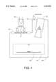
- FIG. 1is a diagram of a dark BEOL process according to the present invention
- FIG. 2is a diagram of an electrolytic cell
- FIG. 3is a cross-sectional view of an exemplary PN junction
- FIG. 4is a cross-sectional view of an exemplary FEOL wafer during BEOL processing.
- test waferswere fabricated using CMP with only metal lines or wiring and no integrated circuit devices.
- Active circuitrysuch as transistors, resistors, capacitors, etc.
- Localized metal corrosionwas observed on the wafers with active circuitry that did not appear on the test wafers without active circuitry. Similar effects were observed in aluminum conductors.
- Corrosionis a process that occurs at open circuit, that is, there is no net flow of current. Rather, both an anodic and a cathodic reaction occur on the surface of the corroding material. These two reactions are interrelated in that the electrical charge passed in each reaction is equal but of opposite sign. Further, if either reaction can be prevented, then the overall corrosion reaction will be prevented.
- the anodic reactioninvolves oxidation, typically of a solid metal, and takes place at the anode.
- oxidation or anodic reactionmay be described as
- Mis a metal atom
- e -is an electron
- nis an integer.
- electronsare produced by oxidation at the anode.
- the cathodic reactioninvolves reduction and takes place at the cathode.
- reduction or cathodic reactionsdepending on the constituents in the electrolyte to which the metal is exposed; a few examples are indicated below.
- the reduction of oxygen to water in acid solutionsmay be described as
- Oxygenmay also be only partially reduced by the pathways
- the reduction reactionmay alternatively be H 2 evolution through
- Equation 8 and 9are combinations of the copper oxidation reaction described generically by Equation 1 and the oxygen reduction reactions described by Equations 2 and 3. Over time, such a reaction will result in pitting and/or dissolution of the copper into solution.
- Electrolysisin contrast to corrosion, is an electrochemical process in which a current source produces a net flow of current.
- the anodic and cathodic reactionstake place in close proximity on the same surface.
- electrolysisthe anodic and cathodic reactions take place on distinctly separated electrodes that are connected to the current source. (See FIG. 2).
- the electrolytic solution to which both electrodes are simultaneously exposedcompletes the electrochemical circuit.
- anodic reactionIn electrolysis, a very large number of anodic and cathodic reactions are possible. In the case of dissolution of metal, the anodic reaction would be Equation 1.
- the anodic reactionis characterized by its thermodynamic reversible potential, E r a .
- E r athe net current flow at equilibrium is zero.
- the potential at which the anodic reaction proceedsis E a , which is E r a + ⁇ a .
- the cathodic reactions pertinent to the inventionmay be equations 2 through 7, and also, if there are metal ions present in the solution:
- electrolysisoccurs when an electrical circuit is formed containing an anode 200 and a cathode 220 both having an internal connection 240 to a current source 210.
- a conduction path between anode 200 and cathode 220is provided through electrolyte 230.
- Currentis conducted through internal connection 240 by electrons or holes and through electrolyte 230 by ions.
- oxidation of the anode metalUpon supplying a sufficient voltage between anode 200 and cathode 220 by current source 210, oxidation of the anode metal (or other anode material) will occur.
- the oxidation reaction at anode 200yields free cations 250 that dissolve into electrolyte 230 and electrons that flow through internal connection 240 to current source 210 and on to cathode 220.
- the oxidation reactioncauses the most visible indicator of electrolysis, that is, dissolution or pitting of anode 200, but a reduction reaction must also occur.
- the reduction reaction at cathode 220combines electrons with reactants 260 in electrolyte 230 to yield the reduced reaction product.
- the reduction reactionmay occur as in Equation 3 where O 2 is the reactant and OH - is the reduced reaction product. Additionally, the reduction reaction may occur as indicated in FIG. 2 and Equations 3 to 7 and Equation 9 where H + , H 2 O, and M n+ may also be reactants 260.
- the anode metalmay dissolve away through a mechanism other than corrosion. The potential required is determined by the thermodynamic reversible potentials and the overpotentials of the anodic and cathodic reactions as discussed above.
- FIG. 3shows an exemplary PN junction 300 that can be used to illustrate what occurs in any of the PN junctions on the wafer.
- PN junction 300includes a p-type semiconductor material 310 juxtaposed with n-type semiconductor material 320.
- Metal interconnects 330, 340are illustrative of metal connectors that may be juxtaposed with any of the n-type or p-type material formed throughout the wafer.
- the metal contactscan serve as contacts to the device of which PN junction 300 is a part.
- One interesting characteristic of PN junctionsis that they exhibit a photovoltaic effect under certain conditions. That is, when exposed to light energy, the electrons in the PN junction are excited into a higher energy level and then, because of a built-in electric field at the junction, the electrons migrate across the interface, producing current. The photovoltaic effect essentially turns PN junction 300 into a battery supplying current to metal interconnects 330, 340. If there is also a surface layer of electrolyte 230 present that can complete the conduction path, then metal interconnects 330, 340 become an anode 330 and a cathode 340.
- the atomic orbitals in effectcombine into continuous "bands" of "crystal” orbitals or electron energy levels.
- the highest occupied bandis called the valence band and the lowest vacant band is called the conduction band.
- the amount of energy required to promote one electron from the highest point in the valence band to the lowest point in the conduction bandis called the band gap energy (E g ).
- E g1.12 eV at room temperature
- E g1.42 eV at room temperature.
- Semiconductive materials, such as siliconare known to exhibit photoconductivity wherein light illumination provides enough energy to excite electrons into the conduction band and to increase the electrical conductivity of the semiconductor.
- hthe Planck constant
- cthe speed of light
- ⁇the frequency
- ⁇ wavelengththe wavelength of light
- ⁇ wavelengththe wavelength of light
- E gthe light energy needed to achieve photoconductivity must reach approximately 1.12 eV or, in other words, have a wavelength less than or equal to approximately 1.1 ⁇ m.
- gallium arsenide semiconductorsphotoconductivity requires a wavelength less than or equal to approximately 0.9 ⁇ m.
- E gis readily available in common references and wavelength can be calculated using the above equations. While the remaining discussion centers on silicon-based semiconductor devices, it will be understood by those skilled in the art that the invention is equally applicable to devices fabricated with other semiconductor materials, such as gallium arsenide.
- a n-type semiconductor 320is silicon doped with a donor impurity, such as phosphorous or arsenic, that donates an electron to the silicon conduction band, creating an extra negative charge carrier. Accordingly, the majority charge carriers in n-type semiconductor 320 are negatively charged particles.
- a p-type semiconductor 310is silicon doped with an acceptor impurity, such as boron, that accepts an electron from the silicon valence band, creating an extra electron hole or positive charge carrier. Accordingly, the majority charge carriers in p-type semiconductor 310 are positively charged electron holes.
- PN junction 300When PN junction 300 is illuminated by photons of light 350 having sufficient energy, electrons are promoted from the valence band to the conduction band in both p-type 310 and n-type 320 semiconductor materials, leaving behind electron holes.
- the additional positive charge carriers thus created in n-type semiconductor 320migrate to the p-type 310 side of junction 300 where the majority charge carriers are positive (electron holes).
- the additional negative charge carriers thus created in p-type semiconductor 310migrate to the n-type 320 side of junction 300 where the majority charge carriers are negative (electrons). This migration of charge carriers constitutes the photovoltaic effect and creates a current source analogous to a battery.
- the electrochemical dissolution of FIG. 3driven by a photovoltage, is analogous to the electrochemical dissolution of FIG. 2.
- the oxidation reaction at anode 330yields free cations 250 that dissolve into electrolyte 230 and electrons that flow through the internal connection to the current source (PN junction 300) and on to cathode 340.
- the oxidation reactioncauses the most visible indicator of electrolysis, that is, dissolution or pitting of anode 330, but a reduction reaction must also occur.
- the reduction reaction at the cathodecombines electrons with reactants 260 in electrolyte 230 to yield the reduced reaction product. Note that some of the metal conductors become anodes and some become cathodes, depending upon whether they are connected to the p side or to the n side of the PN junction.
- a method and apparatus for eliminating or reducing electrochemical dissolution of global wiring, interconnects, contacts, and other metal featuresare provided.
- the preferred embodimentreduces dissolution by eliminating exposure of PN junctions to light capable of invoking a photovoltaic effect and/or inhibiting the oxidation and/or the reduction induced by the photovoltaic effect.
- a preferred embodiment of the method and apparatusare described in FIGS. 1 to 4 and the explanation below.
- FEOLfront-end-of-line
- integrated circuit devicesare formed in silicon wafers. Once the devices are formed, they are connected together with global wiring, interconnects, contacts, and other metal features during back-end-of-line (BEOL) processing.
- BEOLback-end-of-line
- the wiring and interconnectsare formed using a dual damascene process.
- the dual damascene metal processinvolves first etching a trench and contact hole into a dielectric layer on a semiconductor wafer. The wafer is then covered with a conductor, this conductor filling the trench and contact hole and covering the dielectric layer. The wafer is then polished, typically using CMP, down to the dielectric layer. The CMP leaves the conductor embedded as wires and interconnects in the dielectric.
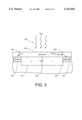
- FIG. 4is a cross-sectional view of a wafer portion 400 formed by dual damascene and CMP and includes exemplary features of typical integrated devices.
- wafer portion 400includes several doped semiconductor regions. The doped regions form n-type and p-type regions that, in turn, define the devices, drains, wells, and contacts for the various transistors.
- wafer portion 400includes many PN junctions.
- STIin FIG. 4 denotes “shallow trench isolation” and “gate” denotes the gate of a field effect transistor (FET).
- FETfield effect transistor
- Wand "Cu” denote conductive material made from tungsten and copper, respectively. The conductive material, in turn, denotes a plurality of wiring and interconnects used to connect the illustrated devices with other devices (not shown) on the wafer portion 400.
- FIG. 4describes two FETs, including the p-type and n-type material associated with the FETs and the STIs separating the FETs, along with the conductive, semiconductive, and insulating material forming other devices on the wafer not shown in the cross-section. Electrolysis as discussed herein may occur in FEOL wafers having device structures entirely different from that shown in FIG. 4, provided the theoretical operation shown in FIG. 3 is present. The importance of FIG. 4 is that it shows p-type and n-type semiconductors juxtaposed and connected with copper interconnects exposed to an electrolyte. When illuminated, the FEOL wafer in FIG. 4 will undergo electrolysis.
- wafer portion 400is typically exposed to light at several instances. While polishing off the blanketed material on the FEOL wafer, the wafer is pressed against a polishing platen and, accordingly, shielded from any light. Once lifted from the platen, during brush cleaning, and during rinsing, the wafer is exposed both to light and to an electrolyte, such as the CMP slurry or water. It was observed that exposure of the wafer after polishing resulted in opens or substantial dissolution of metal features. Upon investigation, it was determined that the dissolution was occurring as a result of electrolysis. Further, the dissolution occurred despite the presence of BTA that previously was sufficient to prevent corrosion of metal features.
- one measure that reduces electrochemical dissolutionis eliminating exposure of PN junctions to light capable of invoking a photovoltaic effect.
- a preferred embodimentprovides implementation of a darkened enclosure 100 shown in FIG. 1, such as a box or curtains, for use on a tool 110 for wafer CMP, brush cleaning, unloading, and rinsing.
- illumination of the wafercan be limited to wavelengths of light that do not provide enough energy to satisfy E g , preventing the promotion of any electrons in the PN junction from the valence band to the conduction band.
- near infrared light at wavelengths of greater than approximately 1.1 ⁇ mmay be used without concern for electrolysis.
- Infrared lightmay be produced by any known method such as placing a visible-block, infrared-pass filter 140 on a light source 150 such as a standard incandescent or halogen lamp.
- the advantage of using infrared lightis that an infrared video camera 160 could then be used for monitoring a "dark" CMP process such as that described.
- a "hot" lightis desired for rapid drying, it may continue provided the wavelength is greater than approximately 1.1 ⁇ m.
- a second measure that reduces electrolysisis inhibiting the oxidation and/or the reduction reaction induced by the photo-generated voltage.
- the inventionprovides use of an inhibitor in the CMP slurry and/or post-CMP water rinse. Using an inhibitor prior to exposure of PN junctions on the wafer to light increases the anodic overpotential, ⁇ a , and/or the cathodic overpotential, ⁇ c .
- the overpotentialscan be increased by, among other mechanisms, passivating the anode, forming a film on the anode, scavenging oxygen from the electrolyte, adsorbing a blocking species on the anode or cathode, and slowing the reaction kinetics of the anodic or cathodic reaction.
- a small amount of a blocking agentis added to interfere with both the oxidation and reduction reactions.
- a suitable blocking agentis a high molecular weight surfactant that will tend to accumulate at the interface between the wafer surface and the electrolyte (CMP slurry or rinse water) and actively bind with the bare metal surfaces. The effect of the surfactant may be to alter the surface environment by displacing water molecules. As a result, the electrode kinetics are slowed both for electrochemical dissolution of metals and for cathodic reactions like oxygen reduction. Impeding the electrode kinetics for either reaction causes an increase in the overpotential and thus a decrease in the current driven by the photovoltage of the PN junction.
- sodium salts of sulfated fatty alcoholsare suitable surfactants, particularly sodium alkyl sulfates, and more particularly sodium octyl sulfate.
- a poisoning agentis used to impede the reduction portion of the electrolysis.
- lead ions, Pb 2+in the CMP electrolyte impede reduction of reactants at the cathode and, thus, affect the overall electrolysis reaction in a manner analogous to that discussed above.
- Other suitable poisoning agentsinclude Bi 3+ , Cd 2+ , Sb 3+ , As 3+ , and Tl 1+ .
- Poisoning species like lead ionsserve to increase the cathodic overpotential Tic because the oxygen reduction reaction can proceed at significant rates only on surfaces that are good catalysts and that lower the energy of activation for the reaction. Absorbed lead ions poison the catalytic activity of the copper surface for oxygen reduction. The lead on the surface prevents the surface interactions that are required to form H 2 O from O 2 . Accordingly then, the reduction portion of electrolysis is inhibited and electrochemical dissolution may be prevented.
Landscapes
- Engineering & Computer Science (AREA)
- Physics & Mathematics (AREA)
- Condensed Matter Physics & Semiconductors (AREA)
- General Physics & Mathematics (AREA)
- Manufacturing & Machinery (AREA)
- Computer Hardware Design (AREA)
- Microelectronics & Electronic Packaging (AREA)
- Power Engineering (AREA)
- Mechanical Engineering (AREA)
- Weting (AREA)
- Mechanical Treatment Of Semiconductor (AREA)
- Cleaning Or Drying Semiconductors (AREA)
Abstract
Description
M→M.sup.n+ +ne.sup.- (Equation 1)
O.sub.2 +4H.sup.+ +4e.sup.- →2H.sub.2 O (Equation 2)
O.sub.2 +2H.sub.2 O+4e.sup.- →4OH.sup.- (Equation 3).
O.sub.2 +2H.sup.+ +2e.sup.- →H.sub.2 O.sub.2 (Equation 4)
O.sub.2 +2H.sub.2 O+2e.sup.- →H.sub.2 O.sub.2 +2OH.sup.-(Equation 5)
2H.sup.+ +2e.sup.- →H.sub.2 (Equation 6)
2H.sub.2 O+2e.sup.- →H.sub.2 +2OH.sup.- (Equation 7)
2Cu+O.sub.2 +4H.sup.+ →2Cu.sup.2+ +2H.sub.2 O (Equation 8)
2Cu+O.sub.2 +2H.sub.2 O→2Cu.sup.2+ +4OH.sup.- (Equation 9)
M.sup.m+ +ne.sup.- →M (Equation 10).
Claims (20)
Priority Applications (5)
| Application Number | Priority Date | Filing Date | Title |
|---|---|---|---|
| US09/020,010US6153043A (en) | 1998-02-06 | 1998-02-06 | Elimination of photo-induced electrochemical dissolution in chemical mechanical polishing |
| KR1019990001059AKR100354593B1 (en) | 1998-02-06 | 1999-01-15 | Elimination of photo-induced electrochemical dissolution in chemical mechanical polishing |
| JP11023639AJP3083809B2 (en) | 1998-02-06 | 1999-02-01 | Apparatus and method for reducing electrolysis of metal features in semiconductor material |
| TW088101471ATW497171B (en) | 1998-02-06 | 1999-02-01 | Elimination of photo-induced electrochemical dissolution in chemical mechanical polishing |
| US09/514,867US6251787B1 (en) | 1998-02-06 | 2000-02-28 | Elimination of photo-induced electrochemical dissolution in chemical mechanical polishing |
Applications Claiming Priority (1)
| Application Number | Priority Date | Filing Date | Title |
|---|---|---|---|
| US09/020,010US6153043A (en) | 1998-02-06 | 1998-02-06 | Elimination of photo-induced electrochemical dissolution in chemical mechanical polishing |
Related Child Applications (1)
| Application Number | Title | Priority Date | Filing Date |
|---|---|---|---|
| US09/514,867DivisionUS6251787B1 (en) | 1998-02-06 | 2000-02-28 | Elimination of photo-induced electrochemical dissolution in chemical mechanical polishing |
Publications (1)
| Publication Number | Publication Date |
|---|---|
| US6153043Atrue US6153043A (en) | 2000-11-28 |
Family
ID=21796270
Family Applications (2)
| Application Number | Title | Priority Date | Filing Date |
|---|---|---|---|
| US09/020,010Expired - LifetimeUS6153043A (en) | 1998-02-06 | 1998-02-06 | Elimination of photo-induced electrochemical dissolution in chemical mechanical polishing |
| US09/514,867Expired - LifetimeUS6251787B1 (en) | 1998-02-06 | 2000-02-28 | Elimination of photo-induced electrochemical dissolution in chemical mechanical polishing |
Family Applications After (1)
| Application Number | Title | Priority Date | Filing Date |
|---|---|---|---|
| US09/514,867Expired - LifetimeUS6251787B1 (en) | 1998-02-06 | 2000-02-28 | Elimination of photo-induced electrochemical dissolution in chemical mechanical polishing |
Country Status (4)
| Country | Link |
|---|---|
| US (2) | US6153043A (en) |
| JP (1) | JP3083809B2 (en) |
| KR (1) | KR100354593B1 (en) |
| TW (1) | TW497171B (en) |
Cited By (58)
| Publication number | Priority date | Publication date | Assignee | Title |
|---|---|---|---|---|
| US6338976B1 (en)* | 2000-01-21 | 2002-01-15 | Taiwan Semiconductor Manufacturing Company, Ltd. | Method for forming optoelectronic microelectronic fabrication with attenuated bond pad corrosion |
| US6376345B1 (en) | 1998-07-24 | 2002-04-23 | Hitachi Ltd. | Process for manufacturing semiconductor integrated circuit device |
| US6402592B1 (en)* | 2001-01-17 | 2002-06-11 | Steag Cutek Systems, Inc. | Electrochemical methods for polishing copper films on semiconductor substrates |
| US6429145B1 (en)* | 2001-01-26 | 2002-08-06 | International Business Machines Corporation | Method of determining electrical properties of silicon-on-insulator wafers |
| US20020113271A1 (en)* | 1999-08-10 | 2002-08-22 | Hitachi, Ltd. | Semiconductor integrated circuit device and manufacturing method of semiconductor integrated circuit device |
| US6509273B1 (en) | 1999-04-28 | 2003-01-21 | Hitachi, Ltd. | Method for manufacturing a semiconductor device |
| US6537144B1 (en) | 2000-02-17 | 2003-03-25 | Applied Materials, Inc. | Method and apparatus for enhanced CMP using metals having reductive properties |
| US20030073385A1 (en)* | 2001-10-12 | 2003-04-17 | International Business Machines Corporation | Self-cleaning colloidal slurry composition and process for finishing a surface of a substrate |
| US20030116445A1 (en)* | 2001-12-21 | 2003-06-26 | Applied Materials, Inc. | Electrolyte with good planarization capability, high removal rate and smooth surface finish for electrochemically controlled copper CMP |
| US20030136684A1 (en)* | 2002-01-22 | 2003-07-24 | Applied Materials, Inc. | Endpoint detection for electro chemical mechanical polishing and electropolishing processes |
| US20030154999A1 (en)* | 2002-02-20 | 2003-08-21 | Taiwan Semiconductor Manufacturing Co., Ltd. | Method for preventing chemical attack on a copper containing semiconductor wafer |
| US20030213703A1 (en)* | 2002-05-16 | 2003-11-20 | Applied Materials, Inc. | Method and apparatus for substrate polishing |
| US20030234184A1 (en)* | 2001-03-14 | 2003-12-25 | Applied Materials, Inc. | Method and composition for polishing a substrate |
| US20040009670A1 (en)* | 2002-06-28 | 2004-01-15 | Axel Preusse | Apparatus and method for reducing oxidation of polished metal surfaces in a chemical mechanical polishing process |
| US20040053512A1 (en)* | 2002-09-16 | 2004-03-18 | Applied Materials, Inc. | Process control in electrochemically assisted planarization |
| US20040053560A1 (en)* | 2002-09-16 | 2004-03-18 | Lizhong Sun | Control of removal profile in electrochemically assisted CMP |
| US20040173461A1 (en)* | 2003-03-04 | 2004-09-09 | Applied Materials, Inc. | Method and apparatus for local polishing control |
| US20040182721A1 (en)* | 2003-03-18 | 2004-09-23 | Applied Materials, Inc. | Process control in electro-chemical mechanical polishing |
| US6811680B2 (en) | 2001-03-14 | 2004-11-02 | Applied Materials Inc. | Planarization of substrates using electrochemical mechanical polishing |
| US20040259352A1 (en)* | 2003-06-17 | 2004-12-23 | Yaojian Leng | Corrosion resistance for copper interconnects |
| US20050059232A1 (en)* | 2003-09-17 | 2005-03-17 | Andreas Michael T. | Method for the post-etch cleaning of multi-level damascene structures having underlying copper metallization |
| US6962524B2 (en) | 2000-02-17 | 2005-11-08 | Applied Materials, Inc. | Conductive polishing article for electrochemical mechanical polishing |
| US6979248B2 (en) | 2002-05-07 | 2005-12-27 | Applied Materials, Inc. | Conductive polishing article for electrochemical mechanical polishing |
| US20060011224A1 (en)* | 2004-07-18 | 2006-01-19 | Chung-Chih Chen | Extrusion free wet cleaning process |
| US6988942B2 (en) | 2000-02-17 | 2006-01-24 | Applied Materials Inc. | Conductive polishing article for electrochemical mechanical polishing |
| US7014538B2 (en) | 1999-05-03 | 2006-03-21 | Applied Materials, Inc. | Article for polishing semiconductor substrates |
| US7029365B2 (en) | 2000-02-17 | 2006-04-18 | Applied Materials Inc. | Pad assembly for electrochemical mechanical processing |
| US7059948B2 (en) | 2000-12-22 | 2006-06-13 | Applied Materials | Articles for polishing semiconductor substrates |
| US7077721B2 (en) | 2000-02-17 | 2006-07-18 | Applied Materials, Inc. | Pad assembly for electrochemical mechanical processing |
| US20060163074A1 (en)* | 2002-09-16 | 2006-07-27 | Applied Materials, Inc. | Algorithm for real-time process control of electro-polishing |
| US20060166500A1 (en)* | 2005-01-26 | 2006-07-27 | Applied Materials, Inc. | Electroprocessing profile control |
| US7084064B2 (en) | 2004-09-14 | 2006-08-01 | Applied Materials, Inc. | Full sequence metal and barrier layer electrochemical mechanical processing |
| US7125477B2 (en) | 2000-02-17 | 2006-10-24 | Applied Materials, Inc. | Contacts for electrochemical processing |
| US7128825B2 (en) | 2001-03-14 | 2006-10-31 | Applied Materials, Inc. | Method and composition for polishing a substrate |
| US7137879B2 (en) | 2001-04-24 | 2006-11-21 | Applied Materials, Inc. | Conductive polishing article for electrochemical mechanical polishing |
| US7160432B2 (en) | 2001-03-14 | 2007-01-09 | Applied Materials, Inc. | Method and composition for polishing a substrate |
| US7186164B2 (en) | 2003-12-03 | 2007-03-06 | Applied Materials, Inc. | Processing pad assembly with zone control |
| US7207878B2 (en) | 2000-02-17 | 2007-04-24 | Applied Materials, Inc. | Conductive polishing article for electrochemical mechanical polishing |
| US20070111402A1 (en)* | 2005-11-16 | 2007-05-17 | Taiwan Semiconductor Manufacturing Company, Ltd. | Production and packaging control for repaired integrated circuits |
| US7303462B2 (en) | 2000-02-17 | 2007-12-04 | Applied Materials, Inc. | Edge bead removal by an electro polishing process |
| US7303662B2 (en) | 2000-02-17 | 2007-12-04 | Applied Materials, Inc. | Contacts for electrochemical processing |
| US20080014709A1 (en)* | 2006-07-07 | 2008-01-17 | Applied Materials, Inc. | Method and apparatus for electroprocessing a substrate with edge profile control |
| US7323095B2 (en) | 2000-12-18 | 2008-01-29 | Applied Materials, Inc. | Integrated multi-step gap fill and all feature planarization for conductive materials |
| US7323416B2 (en) | 2001-03-14 | 2008-01-29 | Applied Materials, Inc. | Method and composition for polishing a substrate |
| US7344432B2 (en) | 2001-04-24 | 2008-03-18 | Applied Materials, Inc. | Conductive pad with ion exchange membrane for electrochemical mechanical polishing |
| US7374644B2 (en) | 2000-02-17 | 2008-05-20 | Applied Materials, Inc. | Conductive polishing article for electrochemical mechanical polishing |
| US20080138962A1 (en)* | 2004-07-22 | 2008-06-12 | Renesas Technology Corp. | Manufacturing Method of Semiconductor Device |
| US7390744B2 (en) | 2004-01-29 | 2008-06-24 | Applied Materials, Inc. | Method and composition for polishing a substrate |
| US7390429B2 (en) | 2003-06-06 | 2008-06-24 | Applied Materials, Inc. | Method and composition for electrochemical mechanical polishing processing |
| US7427340B2 (en) | 2005-04-08 | 2008-09-23 | Applied Materials, Inc. | Conductive pad |
| US20080274596A1 (en)* | 2000-06-08 | 2008-11-06 | Renesas Technology Corporation | Semiconductor device and method of manufacturing the same |
| US20090023231A1 (en)* | 2006-02-01 | 2009-01-22 | Tohoku University | Semiconductor Device Manufacturing Method and Method for Reducing Microroughness of Semiconductor Surface |
| US7520968B2 (en) | 2004-10-05 | 2009-04-21 | Applied Materials, Inc. | Conductive pad design modification for better wafer-pad contact |
| US7582564B2 (en) | 2001-03-14 | 2009-09-01 | Applied Materials, Inc. | Process and composition for conductive material removal by electrochemical mechanical polishing |
| US7670468B2 (en) | 2000-02-17 | 2010-03-02 | Applied Materials, Inc. | Contact assembly and method for electrochemical mechanical processing |
| US7678245B2 (en) | 2000-02-17 | 2010-03-16 | Applied Materials, Inc. | Method and apparatus for electrochemical mechanical processing |
| US7790015B2 (en) | 2002-09-16 | 2010-09-07 | Applied Materials, Inc. | Endpoint for electroprocessing |
| US20100308839A1 (en)* | 2005-08-18 | 2010-12-09 | National University Corporation Tohoku University | Electronic device identifying method |
Families Citing this family (17)
| Publication number | Priority date | Publication date | Assignee | Title |
|---|---|---|---|---|
| JP4513145B2 (en)* | 1999-09-07 | 2010-07-28 | ソニー株式会社 | Semiconductor device manufacturing method and polishing method |
| KR100338777B1 (en)* | 2000-07-22 | 2002-05-31 | 윤종용 | Manufacturing method of semiconductor device for protecting Cu layer from post chemical mechanical polishing-corrosion and chemical mechanical polisher used in the same. |
| JP4742417B2 (en)* | 2000-11-29 | 2011-08-10 | 三菱瓦斯化学株式会社 | Manufacturing method of semiconductor device |
| US6548420B2 (en)* | 2001-01-26 | 2003-04-15 | International Business Machines Corporation | Measurement and analysis of mercury-based pseudo-field effect transistors |
| US6933186B2 (en)* | 2001-09-21 | 2005-08-23 | International Business Machines Corporation | Method for BEOL resistor tolerance improvement using anodic oxidation |
| JP2004063589A (en)* | 2002-07-25 | 2004-02-26 | Ebara Corp | Polishing device |
| US6956281B2 (en) | 2002-08-21 | 2005-10-18 | Freescale Semiconductor, Inc. | Semiconductor device for reducing photovolatic current |
| US6919219B2 (en)* | 2002-11-21 | 2005-07-19 | Texas Instruments Incorporated | Photon-blocking layer |
| US7188630B2 (en)* | 2003-05-07 | 2007-03-13 | Freescale Semiconductor, Inc. | Method to passivate conductive surfaces during semiconductor processing |
| JP4764604B2 (en)* | 2004-01-30 | 2011-09-07 | ルネサスエレクトロニクス株式会社 | Manufacturing method of semiconductor integrated circuit device |
| WO2006125462A1 (en)* | 2005-05-25 | 2006-11-30 | Freescale Semiconductor, Inc | Cleaning solution for a semiconductor wafer |
| JP4861072B2 (en)* | 2006-06-20 | 2012-01-25 | オンセミコンダクター・トレーディング・リミテッド | Semiconductor device and manufacturing method thereof |
| US20100273330A1 (en)* | 2006-08-23 | 2010-10-28 | Citibank N.A. As Collateral Agent | Rinse formulation for use in the manufacture of an integrated circuit |
| US7972873B2 (en)* | 2008-10-27 | 2011-07-05 | Agere Systems Inc. | Material removing processes in device formation and the devices formed thereby |
| US8557703B2 (en)* | 2010-08-12 | 2013-10-15 | Stmicroelectronics, Inc. | Method for pre-migration of metal ions in a semiconductor package |
| US8764515B2 (en)* | 2012-05-14 | 2014-07-01 | United Technologies Corporation | Component machining method and assembly |
| JP6128941B2 (en)* | 2013-05-10 | 2017-05-17 | ルネサスエレクトロニクス株式会社 | Semiconductor device manufacturing method and semiconductor manufacturing apparatus |
Citations (12)
| Publication number | Priority date | Publication date | Assignee | Title |
|---|---|---|---|---|
| JPH01164039A (en)* | 1987-12-21 | 1989-06-28 | Nec Corp | Automatic washing apparatus of semiconductor substrate |
| JPH02257613A (en)* | 1989-03-30 | 1990-10-18 | Fujitsu Ltd | Removal of contamination by fine particle |
| US5084071A (en)* | 1989-03-07 | 1992-01-28 | International Business Machines Corporation | Method of chemical-mechanical polishing an electronic component substrate and polishing slurry therefor |
| US5139571A (en)* | 1991-04-24 | 1992-08-18 | Motorola, Inc. | Non-contaminating wafer polishing slurry |
| US5144498A (en)* | 1990-02-14 | 1992-09-01 | Hewlett-Packard Company | Variable wavelength light filter and sensor system |
| JPH0547735A (en)* | 1991-08-20 | 1993-02-26 | Tadahiro Omi | Cleaning apparatus |
| US5340370A (en)* | 1993-11-03 | 1994-08-23 | Intel Corporation | Slurries for chemical mechanical polishing |
| JPH07256260A (en)* | 1994-03-25 | 1995-10-09 | Nec Corp | Apparatus for treating electrolytic activated water |
| US5480748A (en)* | 1992-10-21 | 1996-01-02 | International Business Machines Corporation | Protection of aluminum metallization against chemical attack during photoresist development |
| US5527423A (en)* | 1994-10-06 | 1996-06-18 | Cabot Corporation | Chemical mechanical polishing slurry for metal layers |
| US5575837A (en)* | 1993-04-28 | 1996-11-19 | Fujimi Incorporated | Polishing composition |
| US5931723A (en)* | 1996-05-29 | 1999-08-03 | Ebara Corporation | Polishing apparatus |
- 1998
- 1998-02-06USUS09/020,010patent/US6153043A/ennot_activeExpired - Lifetime
- 1999
- 1999-01-15KRKR1019990001059Apatent/KR100354593B1/ennot_activeExpired - Lifetime
- 1999-02-01JPJP11023639Apatent/JP3083809B2/ennot_activeExpired - Fee Related
- 1999-02-01TWTW088101471Apatent/TW497171B/ennot_activeIP Right Cessation
- 2000
- 2000-02-28USUS09/514,867patent/US6251787B1/ennot_activeExpired - Lifetime
Patent Citations (12)
| Publication number | Priority date | Publication date | Assignee | Title |
|---|---|---|---|---|
| JPH01164039A (en)* | 1987-12-21 | 1989-06-28 | Nec Corp | Automatic washing apparatus of semiconductor substrate |
| US5084071A (en)* | 1989-03-07 | 1992-01-28 | International Business Machines Corporation | Method of chemical-mechanical polishing an electronic component substrate and polishing slurry therefor |
| JPH02257613A (en)* | 1989-03-30 | 1990-10-18 | Fujitsu Ltd | Removal of contamination by fine particle |
| US5144498A (en)* | 1990-02-14 | 1992-09-01 | Hewlett-Packard Company | Variable wavelength light filter and sensor system |
| US5139571A (en)* | 1991-04-24 | 1992-08-18 | Motorola, Inc. | Non-contaminating wafer polishing slurry |
| JPH0547735A (en)* | 1991-08-20 | 1993-02-26 | Tadahiro Omi | Cleaning apparatus |
| US5480748A (en)* | 1992-10-21 | 1996-01-02 | International Business Machines Corporation | Protection of aluminum metallization against chemical attack during photoresist development |
| US5575837A (en)* | 1993-04-28 | 1996-11-19 | Fujimi Incorporated | Polishing composition |
| US5340370A (en)* | 1993-11-03 | 1994-08-23 | Intel Corporation | Slurries for chemical mechanical polishing |
| JPH07256260A (en)* | 1994-03-25 | 1995-10-09 | Nec Corp | Apparatus for treating electrolytic activated water |
| US5527423A (en)* | 1994-10-06 | 1996-06-18 | Cabot Corporation | Chemical mechanical polishing slurry for metal layers |
| US5931723A (en)* | 1996-05-29 | 1999-08-03 | Ebara Corporation | Polishing apparatus |
Cited By (122)
| Publication number | Priority date | Publication date | Assignee | Title |
|---|---|---|---|---|
| US8129275B2 (en) | 1998-07-24 | 2012-03-06 | Renesas Electronics Corporation | Process for manufacturing semiconductor integrated circuit device |
| US6376345B1 (en) | 1998-07-24 | 2002-04-23 | Hitachi Ltd. | Process for manufacturing semiconductor integrated circuit device |
| US20060141792A1 (en)* | 1998-07-24 | 2006-06-29 | Naofumi Ohashi | Process for manufacturing semiconductor integrated circuit device |
| US6800557B2 (en) | 1998-07-24 | 2004-10-05 | Renesas Technology Corp. | Process for manufacturing semiconductor integrated circuit device |
| US7510970B2 (en)* | 1998-07-24 | 2009-03-31 | Renesas Technology Corp. | Process for manufacturing semiconductor integrated circuit device |
| US6458674B1 (en) | 1998-07-24 | 2002-10-01 | Hitachi, Ltd. | Process for manufacturing semiconductor integrated circuit device |
| US20040152298A1 (en)* | 1998-07-24 | 2004-08-05 | Naofumi Ohashi | Process for manufacturing semiconductor integrated circuit device |
| US7659201B2 (en) | 1998-07-24 | 2010-02-09 | Renesas Technology Corp. | Process for manufacturing semiconductor integrated circuit device |
| US20100136786A1 (en)* | 1998-07-24 | 2010-06-03 | Naofumi Ohashi | Process for manufacturing semiconductor integrated circuit device |
| US6531400B2 (en) | 1998-07-24 | 2003-03-11 | Hitachi, Ltd. | Process for manufacturing semiconductor integrated circuit device |
| US6509273B1 (en) | 1999-04-28 | 2003-01-21 | Hitachi, Ltd. | Method for manufacturing a semiconductor device |
| US7014538B2 (en) | 1999-05-03 | 2006-03-21 | Applied Materials, Inc. | Article for polishing semiconductor substrates |
| US6815330B2 (en) | 1999-08-10 | 2004-11-09 | Renesas Technology Corp. | Semiconductor integrated circuit device and manufacturing method of semiconductor integrated circuit device |
| US6756679B2 (en) | 1999-08-10 | 2004-06-29 | Hitachi, Ltd. | Semiconductor integrated circuit device and manufacturing method of semiconductor integrated circuit device |
| US6864169B2 (en) | 1999-08-10 | 2005-03-08 | Renesas Technology Corp. | Semiconductor integrated circuit device and manufacturing method of semiconductor integrated circuit device |
| US6849535B2 (en) | 1999-08-10 | 2005-02-01 | Renesas Technology Corp. | Semiconductor integrated circuit device and manufacturing method of semiconductor integrated circuit device |
| US20080138979A1 (en)* | 1999-08-10 | 2008-06-12 | Junji Noguchi | Semiconductor integrated circuit device and manufacturing method of semiconductor integrated circuit device |
| US20030017692A1 (en)* | 1999-08-10 | 2003-01-23 | Hitachi, Ltd. | Semiconductor integrated circuit device and manufacturing method of semiconductor integrated circuit device |
| US20020113271A1 (en)* | 1999-08-10 | 2002-08-22 | Hitachi, Ltd. | Semiconductor integrated circuit device and manufacturing method of semiconductor integrated circuit device |
| US6797606B2 (en) | 1999-08-10 | 2004-09-28 | Renesas Technology Corp. | Semiconductor integrated circuit device and manufacturing method of semiconductor integrated circuit device |
| US6797609B2 (en) | 1999-08-10 | 2004-09-28 | Renesas Technology Corp. | Semiconductor integrated circuit device and manufacturing method of semiconductor integrated circuit device |
| US20030001183A1 (en)* | 1999-08-10 | 2003-01-02 | Hitachi, Ltd. | Semiconductor integrated circuit device and manufacturing method of semiconductor integrated circuit device |
| US20020119651A1 (en)* | 1999-08-10 | 2002-08-29 | Hitachi, Ltd. | Semiconductor integrated circuit device and manufacturing method of semiconductor integrated circuit device |
| US20020142576A1 (en)* | 1999-08-10 | 2002-10-03 | Hitachi, Ltd. | Semiconductor integrated circuit device and manufacturing method of semiconductor integrated circuit device |
| US6716749B2 (en) | 1999-08-10 | 2004-04-06 | Renesas Technology Corporation | Semiconductor integrated circuit device and manufacturing method of semiconductor integrated circuit device |
| US6338976B1 (en)* | 2000-01-21 | 2002-01-15 | Taiwan Semiconductor Manufacturing Company, Ltd. | Method for forming optoelectronic microelectronic fabrication with attenuated bond pad corrosion |
| US7569134B2 (en) | 2000-02-17 | 2009-08-04 | Applied Materials, Inc. | Contacts for electrochemical processing |
| US6537144B1 (en) | 2000-02-17 | 2003-03-25 | Applied Materials, Inc. | Method and apparatus for enhanced CMP using metals having reductive properties |
| US7125477B2 (en) | 2000-02-17 | 2006-10-24 | Applied Materials, Inc. | Contacts for electrochemical processing |
| US7670468B2 (en) | 2000-02-17 | 2010-03-02 | Applied Materials, Inc. | Contact assembly and method for electrochemical mechanical processing |
| US7207878B2 (en) | 2000-02-17 | 2007-04-24 | Applied Materials, Inc. | Conductive polishing article for electrochemical mechanical polishing |
| US7678245B2 (en) | 2000-02-17 | 2010-03-16 | Applied Materials, Inc. | Method and apparatus for electrochemical mechanical processing |
| US7278911B2 (en) | 2000-02-17 | 2007-10-09 | Applied Materials, Inc. | Conductive polishing article for electrochemical mechanical polishing |
| US7285036B2 (en) | 2000-02-17 | 2007-10-23 | Applied Materials, Inc. | Pad assembly for electrochemical mechanical polishing |
| US7422516B2 (en) | 2000-02-17 | 2008-09-09 | Applied Materials, Inc. | Conductive polishing article for electrochemical mechanical polishing |
| US7077721B2 (en) | 2000-02-17 | 2006-07-18 | Applied Materials, Inc. | Pad assembly for electrochemical mechanical processing |
| US7137868B2 (en) | 2000-02-17 | 2006-11-21 | Applied Materials, Inc. | Pad assembly for electrochemical mechanical processing |
| US20060148381A1 (en)* | 2000-02-17 | 2006-07-06 | Applied Materials, Inc. | Pad assembly for electrochemical mechanical processing |
| US6988942B2 (en) | 2000-02-17 | 2006-01-24 | Applied Materials Inc. | Conductive polishing article for electrochemical mechanical polishing |
| US6561873B2 (en)* | 2000-02-17 | 2003-05-13 | Applied Materials, Inc. | Method and apparatus for enhanced CMP using metals having reductive properties |
| US7374644B2 (en) | 2000-02-17 | 2008-05-20 | Applied Materials, Inc. | Conductive polishing article for electrochemical mechanical polishing |
| US7303462B2 (en) | 2000-02-17 | 2007-12-04 | Applied Materials, Inc. | Edge bead removal by an electro polishing process |
| US7344431B2 (en) | 2000-02-17 | 2008-03-18 | Applied Materials, Inc. | Pad assembly for electrochemical mechanical processing |
| US7066800B2 (en) | 2000-02-17 | 2006-06-27 | Applied Materials Inc. | Conductive polishing article for electrochemical mechanical polishing |
| US6962524B2 (en) | 2000-02-17 | 2005-11-08 | Applied Materials, Inc. | Conductive polishing article for electrochemical mechanical polishing |
| US7029365B2 (en) | 2000-02-17 | 2006-04-18 | Applied Materials Inc. | Pad assembly for electrochemical mechanical processing |
| US7303662B2 (en) | 2000-02-17 | 2007-12-04 | Applied Materials, Inc. | Contacts for electrochemical processing |
| US7838349B2 (en)* | 2000-06-08 | 2010-11-23 | Renesas Electronics Corporation | Semiconductor device and method of manufacturing the same |
| US20080274596A1 (en)* | 2000-06-08 | 2008-11-06 | Renesas Technology Corporation | Semiconductor device and method of manufacturing the same |
| US7323095B2 (en) | 2000-12-18 | 2008-01-29 | Applied Materials, Inc. | Integrated multi-step gap fill and all feature planarization for conductive materials |
| US7059948B2 (en) | 2000-12-22 | 2006-06-13 | Applied Materials | Articles for polishing semiconductor substrates |
| US6402592B1 (en)* | 2001-01-17 | 2002-06-11 | Steag Cutek Systems, Inc. | Electrochemical methods for polishing copper films on semiconductor substrates |
| US6429145B1 (en)* | 2001-01-26 | 2002-08-06 | International Business Machines Corporation | Method of determining electrical properties of silicon-on-insulator wafers |
| US7232514B2 (en) | 2001-03-14 | 2007-06-19 | Applied Materials, Inc. | Method and composition for polishing a substrate |
| US6811680B2 (en) | 2001-03-14 | 2004-11-02 | Applied Materials Inc. | Planarization of substrates using electrochemical mechanical polishing |
| US20030234184A1 (en)* | 2001-03-14 | 2003-12-25 | Applied Materials, Inc. | Method and composition for polishing a substrate |
| US7323416B2 (en) | 2001-03-14 | 2008-01-29 | Applied Materials, Inc. | Method and composition for polishing a substrate |
| US7160432B2 (en) | 2001-03-14 | 2007-01-09 | Applied Materials, Inc. | Method and composition for polishing a substrate |
| US7128825B2 (en) | 2001-03-14 | 2006-10-31 | Applied Materials, Inc. | Method and composition for polishing a substrate |
| US7582564B2 (en) | 2001-03-14 | 2009-09-01 | Applied Materials, Inc. | Process and composition for conductive material removal by electrochemical mechanical polishing |
| US6899804B2 (en) | 2001-04-10 | 2005-05-31 | Applied Materials, Inc. | Electrolyte composition and treatment for electrolytic chemical mechanical polishing |
| US7344432B2 (en) | 2001-04-24 | 2008-03-18 | Applied Materials, Inc. | Conductive pad with ion exchange membrane for electrochemical mechanical polishing |
| US7137879B2 (en) | 2001-04-24 | 2006-11-21 | Applied Materials, Inc. | Conductive polishing article for electrochemical mechanical polishing |
| US7311592B2 (en) | 2001-04-24 | 2007-12-25 | Applied Materials, Inc. | Conductive polishing article for electrochemical mechanical polishing |
| US20030073385A1 (en)* | 2001-10-12 | 2003-04-17 | International Business Machines Corporation | Self-cleaning colloidal slurry composition and process for finishing a surface of a substrate |
| US7416680B2 (en)* | 2001-10-12 | 2008-08-26 | International Business Machines Corporation | Self-cleaning colloidal slurry composition and process for finishing a surface of a substrate |
| US7384534B2 (en) | 2001-12-21 | 2008-06-10 | Applied Materials, Inc. | Electrolyte with good planarization capability, high removal rate and smooth surface finish for electrochemically controlled copper CMP |
| US20030116445A1 (en)* | 2001-12-21 | 2003-06-26 | Applied Materials, Inc. | Electrolyte with good planarization capability, high removal rate and smooth surface finish for electrochemically controlled copper CMP |
| US6863797B2 (en) | 2001-12-21 | 2005-03-08 | Applied Materials, Inc. | Electrolyte with good planarization capability, high removal rate and smooth surface finish for electrochemically controlled copper CMP |
| US7229535B2 (en) | 2001-12-21 | 2007-06-12 | Applied Materials, Inc. | Hydrogen bubble reduction on the cathode using double-cell designs |
| US20030136684A1 (en)* | 2002-01-22 | 2003-07-24 | Applied Materials, Inc. | Endpoint detection for electro chemical mechanical polishing and electropolishing processes |
| US6837983B2 (en) | 2002-01-22 | 2005-01-04 | Applied Materials, Inc. | Endpoint detection for electro chemical mechanical polishing and electropolishing processes |
| US20030154999A1 (en)* | 2002-02-20 | 2003-08-21 | Taiwan Semiconductor Manufacturing Co., Ltd. | Method for preventing chemical attack on a copper containing semiconductor wafer |
| US6979248B2 (en) | 2002-05-07 | 2005-12-27 | Applied Materials, Inc. | Conductive polishing article for electrochemical mechanical polishing |
| US20030213703A1 (en)* | 2002-05-16 | 2003-11-20 | Applied Materials, Inc. | Method and apparatus for substrate polishing |
| US20040009670A1 (en)* | 2002-06-28 | 2004-01-15 | Axel Preusse | Apparatus and method for reducing oxidation of polished metal surfaces in a chemical mechanical polishing process |
| DE10229000A1 (en)* | 2002-06-28 | 2004-01-29 | Advanced Micro Devices, Inc., Sunnyvale | Device and method for reducing the oxidation of polished metal surfaces in a chemical mechanical polishing process |
| US7070475B2 (en) | 2002-09-16 | 2006-07-04 | Applied Materials | Process control in electrochemically assisted planarization |
| US6991526B2 (en) | 2002-09-16 | 2006-01-31 | Applied Materials, Inc. | Control of removal profile in electrochemically assisted CMP |
| US7294038B2 (en) | 2002-09-16 | 2007-11-13 | Applied Materials, Inc. | Process control in electrochemically assisted planarization |
| US20060163074A1 (en)* | 2002-09-16 | 2006-07-27 | Applied Materials, Inc. | Algorithm for real-time process control of electro-polishing |
| US6848970B2 (en) | 2002-09-16 | 2005-02-01 | Applied Materials, Inc. | Process control in electrochemically assisted planarization |
| US20060237330A1 (en)* | 2002-09-16 | 2006-10-26 | Applied Materials, Inc. | Algorithm for real-time process control of electro-polishing |
| US7790015B2 (en) | 2002-09-16 | 2010-09-07 | Applied Materials, Inc. | Endpoint for electroprocessing |
| US7628905B2 (en) | 2002-09-16 | 2009-12-08 | Applied Materials, Inc. | Algorithm for real-time process control of electro-polishing |
| US20040053512A1 (en)* | 2002-09-16 | 2004-03-18 | Applied Materials, Inc. | Process control in electrochemically assisted planarization |
| US20040053560A1 (en)* | 2002-09-16 | 2004-03-18 | Lizhong Sun | Control of removal profile in electrochemically assisted CMP |
| US7112270B2 (en) | 2002-09-16 | 2006-09-26 | Applied Materials, Inc. | Algorithm for real-time process control of electro-polishing |
| US20040173461A1 (en)* | 2003-03-04 | 2004-09-09 | Applied Materials, Inc. | Method and apparatus for local polishing control |
| US20040182721A1 (en)* | 2003-03-18 | 2004-09-23 | Applied Materials, Inc. | Process control in electro-chemical mechanical polishing |
| US20080017521A1 (en)* | 2003-03-18 | 2008-01-24 | Manens Antoine P | Process control in electro-chemical mechanical polishing |
| US7390429B2 (en) | 2003-06-06 | 2008-06-24 | Applied Materials, Inc. | Method and composition for electrochemical mechanical polishing processing |
| US6908851B2 (en) | 2003-06-17 | 2005-06-21 | Texas Instruments Incorporated | Corrosion resistance for copper interconnects |
| US20040259352A1 (en)* | 2003-06-17 | 2004-12-23 | Yaojian Leng | Corrosion resistance for copper interconnects |
| US20060003589A1 (en)* | 2003-09-17 | 2006-01-05 | Andreas Michael T | Method for the post-etch cleaning of multi-level damascene structures having underlying copper metallization |
| US20050059232A1 (en)* | 2003-09-17 | 2005-03-17 | Andreas Michael T. | Method for the post-etch cleaning of multi-level damascene structures having underlying copper metallization |
| US6936534B2 (en)* | 2003-09-17 | 2005-08-30 | Micron Technology, Inc. | Method for the post-etch cleaning of multi-level damascene structures having underlying copper metallization |
| US7186164B2 (en) | 2003-12-03 | 2007-03-06 | Applied Materials, Inc. | Processing pad assembly with zone control |
| US7390744B2 (en) | 2004-01-29 | 2008-06-24 | Applied Materials, Inc. | Method and composition for polishing a substrate |
| US20060011224A1 (en)* | 2004-07-18 | 2006-01-19 | Chung-Chih Chen | Extrusion free wet cleaning process |
| US7998793B2 (en) | 2004-07-22 | 2011-08-16 | Renesas Electronics Corporation | Light illumination during wafer dicing to prevent aluminum corrosion |
| US20080138962A1 (en)* | 2004-07-22 | 2008-06-12 | Renesas Technology Corp. | Manufacturing Method of Semiconductor Device |
| US20090215247A1 (en)* | 2004-07-22 | 2009-08-27 | Renesas Technology Corp. | Manufacturing method of semiconductor device |
| US7446041B2 (en) | 2004-09-14 | 2008-11-04 | Applied Materials, Inc. | Full sequence metal and barrier layer electrochemical mechanical processing |
| US7084064B2 (en) | 2004-09-14 | 2006-08-01 | Applied Materials, Inc. | Full sequence metal and barrier layer electrochemical mechanical processing |
| US7520968B2 (en) | 2004-10-05 | 2009-04-21 | Applied Materials, Inc. | Conductive pad design modification for better wafer-pad contact |
| US7709382B2 (en) | 2005-01-26 | 2010-05-04 | Applied Materials, Inc. | Electroprocessing profile control |
| US20060166500A1 (en)* | 2005-01-26 | 2006-07-27 | Applied Materials, Inc. | Electroprocessing profile control |
| US20080045012A1 (en)* | 2005-01-26 | 2008-02-21 | Manens Antoine P | Electroprocessing profile control |
| US7655565B2 (en) | 2005-01-26 | 2010-02-02 | Applied Materials, Inc. | Electroprocessing profile control |
| US20080047841A1 (en)* | 2005-01-26 | 2008-02-28 | Manens Antoine P | Electroprocessing profile control |
| US7427340B2 (en) | 2005-04-08 | 2008-09-23 | Applied Materials, Inc. | Conductive pad |
| US8093918B2 (en)* | 2005-08-18 | 2012-01-10 | National University Corporation Tohoku University | Electronic device identifying method and electronic device comprising identification means |
| US20100308839A1 (en)* | 2005-08-18 | 2010-12-09 | National University Corporation Tohoku University | Electronic device identifying method |
| US20070111402A1 (en)* | 2005-11-16 | 2007-05-17 | Taiwan Semiconductor Manufacturing Company, Ltd. | Production and packaging control for repaired integrated circuits |
| US7521266B2 (en) | 2005-11-16 | 2009-04-21 | Taiwan Semiconductor Manufacturing Company, Ltd. | Production and packaging control for repaired integrated circuits |
| US20090023231A1 (en)* | 2006-02-01 | 2009-01-22 | Tohoku University | Semiconductor Device Manufacturing Method and Method for Reducing Microroughness of Semiconductor Surface |
| EP1988567A4 (en)* | 2006-02-01 | 2009-12-02 | Univ Tohoku | METHOD FOR MANUFACTURING SEMICONDUCTOR DEVICE AND METHOD FOR REDUCING SEMICONDUCTOR SURFACE MICRORUGOSITY |
| US8268735B2 (en)* | 2006-02-01 | 2012-09-18 | Tohoku University | Semiconductor device manufacturing method and method for reducing microroughness of semiconductor surface |
| US20080014709A1 (en)* | 2006-07-07 | 2008-01-17 | Applied Materials, Inc. | Method and apparatus for electroprocessing a substrate with edge profile control |
| US20080035474A1 (en)* | 2006-07-07 | 2008-02-14 | You Wang | Apparatus for electroprocessing a substrate with edge profile control |
| US7422982B2 (en) | 2006-07-07 | 2008-09-09 | Applied Materials, Inc. | Method and apparatus for electroprocessing a substrate with edge profile control |
Also Published As
| Publication number | Publication date |
|---|---|
| KR100354593B1 (en) | 2002-09-30 |
| TW497171B (en) | 2002-08-01 |
| JPH11274114A (en) | 1999-10-08 |
| JP3083809B2 (en) | 2000-09-04 |
| US6251787B1 (en) | 2001-06-26 |
| KR19990072266A (en) | 1999-09-27 |
Similar Documents
| Publication | Publication Date | Title |
|---|---|---|
| US6153043A (en) | Elimination of photo-induced electrochemical dissolution in chemical mechanical polishing | |
| US6800557B2 (en) | Process for manufacturing semiconductor integrated circuit device | |
| US6586161B2 (en) | Mass production method of semiconductor integrated circuit device and manufacturing method of electronic device | |
| US6165279A (en) | Method for cleaning a semiconductor wafer | |
| US6727187B2 (en) | Fabrication method for semiconductor device | |
| US6992009B2 (en) | Method of manufacturing a semiconductor device | |
| US6251771B1 (en) | Hydrogen passivation of chemical-mechanically polished copper-containing layers | |
| US20040036150A1 (en) | Semiconductor device for reducing photovolatic current | |
| US6965136B2 (en) | Photon-blocking layer | |
| Song et al. | Copper corrosion issue and analysis on copper damascene process | |
| JP4764604B2 (en) | Manufacturing method of semiconductor integrated circuit device | |
| Claeys et al. | Source of Metals in Si and Ge Crystal Growth and Processing | |
| Dornisch et al. | Cu contamination control for advanced interconnect manufacturing. | |
| JP2004172617A (en) | Photon inhibition layer | |
| JP2004104137A (en) | Method for manufacturing semiconductor integrated circuit device | |
| Baiocchi et al. | Voiding in Cu technology through photovoltaic-driven electrochemical dissolution | |
| KR20040083622A (en) | Metal wiring forming method of semiconductor device | |
| JP2008021703A (en) | Semiconductor device and manufacturing method thereof |
Legal Events
| Date | Code | Title | Description |
|---|---|---|---|
| AS | Assignment | Owner name:INTERNATIONAL BUSINESS MACHINES CORPORATION, NEW Y Free format text:ASSIGNMENT OF ASSIGNORS INTEREST;ASSIGNORS:EDELSTEIN, DANIEL C.;HORKANS, WILMA J.;LUCE, STEPHEN E.;AND OTHERS;REEL/FRAME:008976/0410;SIGNING DATES FROM 19980127 TO 19980206 | |
| FEPP | Fee payment procedure | Free format text:PAYOR NUMBER ASSIGNED (ORIGINAL EVENT CODE: ASPN); ENTITY STATUS OF PATENT OWNER: LARGE ENTITY | |
| STCF | Information on status: patent grant | Free format text:PATENTED CASE | |
| FEPP | Fee payment procedure | Free format text:PAYOR NUMBER ASSIGNED (ORIGINAL EVENT CODE: ASPN); ENTITY STATUS OF PATENT OWNER: LARGE ENTITY Free format text:PAYER NUMBER DE-ASSIGNED (ORIGINAL EVENT CODE: RMPN); ENTITY STATUS OF PATENT OWNER: LARGE ENTITY | |
| FEPP | Fee payment procedure | Free format text:PAYOR NUMBER ASSIGNED (ORIGINAL EVENT CODE: ASPN); ENTITY STATUS OF PATENT OWNER: LARGE ENTITY Free format text:PAYER NUMBER DE-ASSIGNED (ORIGINAL EVENT CODE: RMPN); ENTITY STATUS OF PATENT OWNER: LARGE ENTITY | |
| FPAY | Fee payment | Year of fee payment:4 | |
| FEPP | Fee payment procedure | Free format text:PAYER NUMBER DE-ASSIGNED (ORIGINAL EVENT CODE: RMPN); ENTITY STATUS OF PATENT OWNER: LARGE ENTITY Free format text:PAYOR NUMBER ASSIGNED (ORIGINAL EVENT CODE: ASPN); ENTITY STATUS OF PATENT OWNER: LARGE ENTITY | |
| FPAY | Fee payment | Year of fee payment:8 | |
| AS | Assignment | Owner name:EBARA CORPORATION, JAPAN Free format text:ASSIGNMENT OF ASSIGNORS INTEREST;ASSIGNOR:INTERNATIONAL BUSINESS MACHINES CORPORATION;REEL/FRAME:021172/0929 Effective date:20080228 | |
| FPAY | Fee payment | Year of fee payment:12 |