US6150717A - Direct die contact (DDC) semiconductor package - Google Patents
Direct die contact (DDC) semiconductor packageDownload PDFInfo
- Publication number
- US6150717A US6150717AUS09/098,197US9819798AUS6150717AUS 6150717 AUS6150717 AUS 6150717AUS 9819798 AUS9819798 AUS 9819798AUS 6150717 AUS6150717 AUS 6150717A
- Authority
- US
- United States
- Prior art keywords
- bumps
- solder
- die
- package
- dice
- Prior art date
- Legal status (The legal status is an assumption and is not a legal conclusion. Google has not performed a legal analysis and makes no representation as to the accuracy of the status listed.)
- Expired - Lifetime
Links
- 239000004065semiconductorSubstances0.000titleclaimsabstractdescription48
- 229910000679solderInorganic materials0.000claimsabstractdescription149
- 239000000853adhesiveSubstances0.000claimsabstractdescription30
- 230000001070adhesive effectEffects0.000claimsabstractdescription30
- 238000004891communicationMethods0.000claimsabstractdescription13
- 239000000758substrateSubstances0.000claimsdescription35
- 229910052751metalInorganic materials0.000claimsdescription28
- 239000002184metalSubstances0.000claimsdescription28
- 230000008018meltingEffects0.000claimsdescription17
- 238000002844meltingMethods0.000claimsdescription17
- 229910045601alloyInorganic materials0.000claimsdescription15
- 239000000956alloySubstances0.000claimsdescription15
- 229910052718tinInorganic materials0.000claimsdescription12
- 239000000463materialSubstances0.000claimsdescription9
- 229910052745leadInorganic materials0.000claimsdescription8
- 229910052763palladiumInorganic materials0.000claimsdescription8
- 229910052737goldInorganic materials0.000claimsdescription6
- 229910052759nickelInorganic materials0.000claimsdescription4
- 229910052782aluminiumInorganic materials0.000claimsdescription3
- 229910052804chromiumInorganic materials0.000claimsdescription3
- 229910052725zincInorganic materials0.000claimsdescription3
- 229910052738indiumInorganic materials0.000claimsdescription2
- 229920000642polymerPolymers0.000claimsdescription2
- XAGFODPZIPBFFR-UHFFFAOYSA-NaluminiumChemical compound[Al]XAGFODPZIPBFFR-UHFFFAOYSA-N0.000claims1
- 238000000034methodMethods0.000abstractdescription35
- 238000005476solderingMethods0.000abstractdescription18
- 230000008021depositionEffects0.000abstractdescription12
- 238000012360testing methodMethods0.000abstractdescription10
- 238000000151depositionMethods0.000description17
- 238000002161passivationMethods0.000description13
- KDLHZDBZIXYQEI-UHFFFAOYSA-NpalladiumSubstances[Pd]KDLHZDBZIXYQEI-UHFFFAOYSA-N0.000description11
- 230000008569processEffects0.000description10
- 239000004020conductorSubstances0.000description7
- 238000003780insertionMethods0.000description7
- 230000037431insertionEffects0.000description7
- 230000004913activationEffects0.000description5
- 239000000919ceramicSubstances0.000description4
- 238000009472formulationMethods0.000description4
- 238000001465metallisationMethods0.000description4
- 239000000203mixtureSubstances0.000description4
- 238000004806packaging method and processMethods0.000description4
- XUIMIQQOPSSXEZ-UHFFFAOYSA-NSiliconChemical compound[Si]XUIMIQQOPSSXEZ-UHFFFAOYSA-N0.000description3
- 238000001723curingMethods0.000description3
- 238000007772electroless platingMethods0.000description3
- 239000010931goldSubstances0.000description3
- 238000004519manufacturing processMethods0.000description3
- PXHVJJICTQNCMI-UHFFFAOYSA-NnickelSubstances[Ni]PXHVJJICTQNCMI-UHFFFAOYSA-N0.000description3
- 229910052710siliconInorganic materials0.000description3
- 239000010703siliconSubstances0.000description3
- SDVHRXOTTYYKRY-UHFFFAOYSA-Jtetrasodium;dioxido-oxo-phosphonato-$l^{5}-phosphaneChemical compound[Na+].[Na+].[Na+].[Na+].[O-]P([O-])(=O)P([O-])([O-])=OSDVHRXOTTYYKRY-UHFFFAOYSA-J0.000description3
- 101100493706Caenorhabditis elegans bath-38 geneProteins0.000description2
- VYPSYNLAJGMNEJ-UHFFFAOYSA-NSilicium dioxideChemical compoundO=[Si]=OVYPSYNLAJGMNEJ-UHFFFAOYSA-N0.000description2
- 230000003213activating effectEffects0.000description2
- 230000015572biosynthetic processEffects0.000description2
- 239000005380borophosphosilicate glassSubstances0.000description2
- 238000007906compressionMethods0.000description2
- 230000006835compressionEffects0.000description2
- 238000010586diagramMethods0.000description2
- 239000010408filmSubstances0.000description2
- PIBWKRNGBLPSSY-UHFFFAOYSA-Lpalladium(II) chlorideChemical compoundCl[Pd]ClPIBWKRNGBLPSSY-UHFFFAOYSA-L0.000description2
- 239000002245particleSubstances0.000description2
- 238000011160researchMethods0.000description2
- NWONKYPBYAMBJT-UHFFFAOYSA-Lzinc sulfateChemical compound[Zn+2].[O-]S([O-])(=O)=ONWONKYPBYAMBJT-UHFFFAOYSA-L0.000description2
- 229910021586Nickel(II) chlorideInorganic materials0.000description1
- 229910007277Si3 N4Inorganic materials0.000description1
- 238000000637aluminium metallisationMethods0.000description1
- DMFGNRRURHSENX-UHFFFAOYSA-Nberyllium copperChemical compound[Be].[Cu]DMFGNRRURHSENX-UHFFFAOYSA-N0.000description1
- 239000011651chromiumSubstances0.000description1
- 238000004140cleaningMethods0.000description1
- 239000011248coating agentSubstances0.000description1
- 238000000576coating methodMethods0.000description1
- 229910052681coesiteInorganic materials0.000description1
- 238000001816coolingMethods0.000description1
- 229910052906cristobaliteInorganic materials0.000description1
- 230000001419dependent effectEffects0.000description1
- 239000012777electrically insulating materialSubstances0.000description1
- 239000008393encapsulating agentSubstances0.000description1
- 238000005516engineering processMethods0.000description1
- 239000006023eutectic alloySubstances0.000description1
- 239000011521glassSubstances0.000description1
- PCHJSUWPFVWCPO-UHFFFAOYSA-NgoldChemical compound[Au]PCHJSUWPFVWCPO-UHFFFAOYSA-N0.000description1
- 238000013007heat curingMethods0.000description1
- 238000010438heat treatmentMethods0.000description1
- BHEPBYXIRTUNPN-UHFFFAOYSA-Nhydridophosphorus(.) (triplet)Chemical compound[PH]BHEPBYXIRTUNPN-UHFFFAOYSA-N0.000description1
- 239000007791liquid phaseSubstances0.000description1
- 239000011159matrix materialSubstances0.000description1
- 230000007246mechanismEffects0.000description1
- 150000002739metalsChemical class0.000description1
- 238000012986modificationMethods0.000description1
- 230000004048modificationEffects0.000description1
- QMMRZOWCJAIUJA-UHFFFAOYSA-Lnickel dichlorideChemical compoundCl[Ni]ClQMMRZOWCJAIUJA-UHFFFAOYSA-L0.000description1
- 150000004767nitridesChemical class0.000description1
- 230000002093peripheral effectEffects0.000description1
- LLHKCFNBLRBOGN-UHFFFAOYSA-Npropylene glycol methyl ether acetateChemical compoundCOCC(C)OC(C)=OLLHKCFNBLRBOGN-UHFFFAOYSA-N0.000description1
- 239000012858resilient materialSubstances0.000description1
- 239000011347resinSubstances0.000description1
- 229920005989resinPolymers0.000description1
- 238000007650screen-printingMethods0.000description1
- 239000005368silicate glassSubstances0.000description1
- 239000000377silicon dioxideSubstances0.000description1
- VILMUCRZVVVJCA-UHFFFAOYSA-Msodium glycolateChemical compound[Na+].OCC([O-])=OVILMUCRZVVVJCA-UHFFFAOYSA-M0.000description1
- 229910052682stishoviteInorganic materials0.000description1
- 239000000126substanceSubstances0.000description1
- 239000010409thin filmSubstances0.000description1
- 229910052905tridymiteInorganic materials0.000description1
- 239000012808vapor phaseSubstances0.000description1
- 235000012431wafersNutrition0.000description1
- 239000011701zincSubstances0.000description1
Images


Classifications
- H—ELECTRICITY
- H01—ELECTRIC ELEMENTS
- H01L—SEMICONDUCTOR DEVICES NOT COVERED BY CLASS H10
- H01L24/00—Arrangements for connecting or disconnecting semiconductor or solid-state bodies; Methods or apparatus related thereto
- H01L24/80—Methods for connecting semiconductor or other solid state bodies using means for bonding being attached to, or being formed on, the surface to be connected
- H01L24/81—Methods for connecting semiconductor or other solid state bodies using means for bonding being attached to, or being formed on, the surface to be connected using a bump connector
- H—ELECTRICITY
- H01—ELECTRIC ELEMENTS
- H01L—SEMICONDUCTOR DEVICES NOT COVERED BY CLASS H10
- H01L24/00—Arrangements for connecting or disconnecting semiconductor or solid-state bodies; Methods or apparatus related thereto
- H01L24/01—Means for bonding being attached to, or being formed on, the surface to be connected, e.g. chip-to-package, die-attach, "first-level" interconnects; Manufacturing methods related thereto
- H01L24/10—Bump connectors ; Manufacturing methods related thereto
- H01L24/11—Manufacturing methods
- H—ELECTRICITY
- H01—ELECTRIC ELEMENTS
- H01L—SEMICONDUCTOR DEVICES NOT COVERED BY CLASS H10
- H01L24/00—Arrangements for connecting or disconnecting semiconductor or solid-state bodies; Methods or apparatus related thereto
- H01L24/01—Means for bonding being attached to, or being formed on, the surface to be connected, e.g. chip-to-package, die-attach, "first-level" interconnects; Manufacturing methods related thereto
- H01L24/10—Bump connectors ; Manufacturing methods related thereto
- H01L24/12—Structure, shape, material or disposition of the bump connectors prior to the connecting process
- H01L24/13—Structure, shape, material or disposition of the bump connectors prior to the connecting process of an individual bump connector
- H—ELECTRICITY
- H01—ELECTRIC ELEMENTS
- H01L—SEMICONDUCTOR DEVICES NOT COVERED BY CLASS H10
- H01L2224/00—Indexing scheme for arrangements for connecting or disconnecting semiconductor or solid-state bodies and methods related thereto as covered by H01L24/00
- H01L2224/01—Means for bonding being attached to, or being formed on, the surface to be connected, e.g. chip-to-package, die-attach, "first-level" interconnects; Manufacturing methods related thereto
- H01L2224/02—Bonding areas; Manufacturing methods related thereto
- H01L2224/04—Structure, shape, material or disposition of the bonding areas prior to the connecting process
- H01L2224/05—Structure, shape, material or disposition of the bonding areas prior to the connecting process of an individual bonding area
- H01L2224/05001—Internal layers
- H01L2224/0502—Disposition
- H01L2224/05022—Disposition the internal layer being at least partially embedded in the surface
- H—ELECTRICITY
- H01—ELECTRIC ELEMENTS
- H01L—SEMICONDUCTOR DEVICES NOT COVERED BY CLASS H10
- H01L2224/00—Indexing scheme for arrangements for connecting or disconnecting semiconductor or solid-state bodies and methods related thereto as covered by H01L24/00
- H01L2224/01—Means for bonding being attached to, or being formed on, the surface to be connected, e.g. chip-to-package, die-attach, "first-level" interconnects; Manufacturing methods related thereto
- H01L2224/02—Bonding areas; Manufacturing methods related thereto
- H01L2224/04—Structure, shape, material or disposition of the bonding areas prior to the connecting process
- H01L2224/05—Structure, shape, material or disposition of the bonding areas prior to the connecting process of an individual bonding area
- H01L2224/05001—Internal layers
- H01L2224/0502—Disposition
- H01L2224/05026—Disposition the internal layer being disposed in a recess of the surface
- H—ELECTRICITY
- H01—ELECTRIC ELEMENTS
- H01L—SEMICONDUCTOR DEVICES NOT COVERED BY CLASS H10
- H01L2224/00—Indexing scheme for arrangements for connecting or disconnecting semiconductor or solid-state bodies and methods related thereto as covered by H01L24/00
- H01L2224/01—Means for bonding being attached to, or being formed on, the surface to be connected, e.g. chip-to-package, die-attach, "first-level" interconnects; Manufacturing methods related thereto
- H01L2224/02—Bonding areas; Manufacturing methods related thereto
- H01L2224/04—Structure, shape, material or disposition of the bonding areas prior to the connecting process
- H01L2224/05—Structure, shape, material or disposition of the bonding areas prior to the connecting process of an individual bonding area
- H01L2224/0554—External layer
- H01L2224/0556—Disposition
- H01L2224/05571—Disposition the external layer being disposed in a recess of the surface
- H—ELECTRICITY
- H01—ELECTRIC ELEMENTS
- H01L—SEMICONDUCTOR DEVICES NOT COVERED BY CLASS H10
- H01L2224/00—Indexing scheme for arrangements for connecting or disconnecting semiconductor or solid-state bodies and methods related thereto as covered by H01L24/00
- H01L2224/01—Means for bonding being attached to, or being formed on, the surface to be connected, e.g. chip-to-package, die-attach, "first-level" interconnects; Manufacturing methods related thereto
- H01L2224/10—Bump connectors; Manufacturing methods related thereto
- H01L2224/1012—Auxiliary members for bump connectors, e.g. spacers
- H01L2224/10152—Auxiliary members for bump connectors, e.g. spacers being formed on an item to be connected not being a semiconductor or solid-state body
- H01L2224/10165—Alignment aids
- H—ELECTRICITY
- H01—ELECTRIC ELEMENTS
- H01L—SEMICONDUCTOR DEVICES NOT COVERED BY CLASS H10
- H01L2224/00—Indexing scheme for arrangements for connecting or disconnecting semiconductor or solid-state bodies and methods related thereto as covered by H01L24/00
- H01L2224/01—Means for bonding being attached to, or being formed on, the surface to be connected, e.g. chip-to-package, die-attach, "first-level" interconnects; Manufacturing methods related thereto
- H01L2224/10—Bump connectors; Manufacturing methods related thereto
- H01L2224/12—Structure, shape, material or disposition of the bump connectors prior to the connecting process
- H01L2224/13—Structure, shape, material or disposition of the bump connectors prior to the connecting process of an individual bump connector
- H01L2224/13001—Core members of the bump connector
- H01L2224/13099—Material
- H01L2224/131—Material with a principal constituent of the material being a metal or a metalloid, e.g. boron [B], silicon [Si], germanium [Ge], arsenic [As], antimony [Sb], tellurium [Te] and polonium [Po], and alloys thereof
- H—ELECTRICITY
- H01—ELECTRIC ELEMENTS
- H01L—SEMICONDUCTOR DEVICES NOT COVERED BY CLASS H10
- H01L2224/00—Indexing scheme for arrangements for connecting or disconnecting semiconductor or solid-state bodies and methods related thereto as covered by H01L24/00
- H01L2224/01—Means for bonding being attached to, or being formed on, the surface to be connected, e.g. chip-to-package, die-attach, "first-level" interconnects; Manufacturing methods related thereto
- H01L2224/10—Bump connectors; Manufacturing methods related thereto
- H01L2224/12—Structure, shape, material or disposition of the bump connectors prior to the connecting process
- H01L2224/13—Structure, shape, material or disposition of the bump connectors prior to the connecting process of an individual bump connector
- H01L2224/13001—Core members of the bump connector
- H01L2224/13099—Material
- H01L2224/1319—Material with a principal constituent of the material being a polymer, e.g. polyester, phenolic based polymer, epoxy
- H—ELECTRICITY
- H01—ELECTRIC ELEMENTS
- H01L—SEMICONDUCTOR DEVICES NOT COVERED BY CLASS H10
- H01L2224/00—Indexing scheme for arrangements for connecting or disconnecting semiconductor or solid-state bodies and methods related thereto as covered by H01L24/00
- H01L2224/01—Means for bonding being attached to, or being formed on, the surface to be connected, e.g. chip-to-package, die-attach, "first-level" interconnects; Manufacturing methods related thereto
- H01L2224/10—Bump connectors; Manufacturing methods related thereto
- H01L2224/15—Structure, shape, material or disposition of the bump connectors after the connecting process
- H01L2224/16—Structure, shape, material or disposition of the bump connectors after the connecting process of an individual bump connector
- H01L2224/161—Disposition
- H01L2224/16151—Disposition the bump connector connecting between a semiconductor or solid-state body and an item not being a semiconductor or solid-state body, e.g. chip-to-substrate, chip-to-passive
- H01L2224/16221—Disposition the bump connector connecting between a semiconductor or solid-state body and an item not being a semiconductor or solid-state body, e.g. chip-to-substrate, chip-to-passive the body and the item being stacked
- H01L2224/16225—Disposition the bump connector connecting between a semiconductor or solid-state body and an item not being a semiconductor or solid-state body, e.g. chip-to-substrate, chip-to-passive the body and the item being stacked the item being non-metallic, e.g. insulating substrate with or without metallisation
- H01L2224/16237—Disposition the bump connector connecting between a semiconductor or solid-state body and an item not being a semiconductor or solid-state body, e.g. chip-to-substrate, chip-to-passive the body and the item being stacked the item being non-metallic, e.g. insulating substrate with or without metallisation the bump connector connecting to a bonding area disposed in a recess of the surface of the item
- H—ELECTRICITY
- H01—ELECTRIC ELEMENTS
- H01L—SEMICONDUCTOR DEVICES NOT COVERED BY CLASS H10
- H01L2224/00—Indexing scheme for arrangements for connecting or disconnecting semiconductor or solid-state bodies and methods related thereto as covered by H01L24/00
- H01L2224/80—Methods for connecting semiconductor or other solid state bodies using means for bonding being attached to, or being formed on, the surface to be connected
- H01L2224/81—Methods for connecting semiconductor or other solid state bodies using means for bonding being attached to, or being formed on, the surface to be connected using a bump connector
- H01L2224/8112—Aligning
- H01L2224/81136—Aligning involving guiding structures, e.g. spacers or supporting members
- H01L2224/81138—Aligning involving guiding structures, e.g. spacers or supporting members the guiding structures being at least partially left in the finished device
- H01L2224/8114—Guiding structures outside the body
- H—ELECTRICITY
- H01—ELECTRIC ELEMENTS
- H01L—SEMICONDUCTOR DEVICES NOT COVERED BY CLASS H10
- H01L2224/00—Indexing scheme for arrangements for connecting or disconnecting semiconductor or solid-state bodies and methods related thereto as covered by H01L24/00
- H01L2224/80—Methods for connecting semiconductor or other solid state bodies using means for bonding being attached to, or being formed on, the surface to be connected
- H01L2224/81—Methods for connecting semiconductor or other solid state bodies using means for bonding being attached to, or being formed on, the surface to be connected using a bump connector
- H01L2224/8119—Arrangement of the bump connectors prior to mounting
- H01L2224/81191—Arrangement of the bump connectors prior to mounting wherein the bump connectors are disposed only on the semiconductor or solid-state body
- H—ELECTRICITY
- H01—ELECTRIC ELEMENTS
- H01L—SEMICONDUCTOR DEVICES NOT COVERED BY CLASS H10
- H01L2224/00—Indexing scheme for arrangements for connecting or disconnecting semiconductor or solid-state bodies and methods related thereto as covered by H01L24/00
- H01L2224/80—Methods for connecting semiconductor or other solid state bodies using means for bonding being attached to, or being formed on, the surface to be connected
- H01L2224/81—Methods for connecting semiconductor or other solid state bodies using means for bonding being attached to, or being formed on, the surface to be connected using a bump connector
- H01L2224/8119—Arrangement of the bump connectors prior to mounting
- H01L2224/81192—Arrangement of the bump connectors prior to mounting wherein the bump connectors are disposed only on another item or body to be connected to the semiconductor or solid-state body
- H—ELECTRICITY
- H01—ELECTRIC ELEMENTS
- H01L—SEMICONDUCTOR DEVICES NOT COVERED BY CLASS H10
- H01L2224/00—Indexing scheme for arrangements for connecting or disconnecting semiconductor or solid-state bodies and methods related thereto as covered by H01L24/00
- H01L2224/80—Methods for connecting semiconductor or other solid state bodies using means for bonding being attached to, or being formed on, the surface to be connected
- H01L2224/81—Methods for connecting semiconductor or other solid state bodies using means for bonding being attached to, or being formed on, the surface to be connected using a bump connector
- H01L2224/8119—Arrangement of the bump connectors prior to mounting
- H01L2224/81193—Arrangement of the bump connectors prior to mounting wherein the bump connectors are disposed on both the semiconductor or solid-state body and another item or body to be connected to the semiconductor or solid-state body
- H—ELECTRICITY
- H01—ELECTRIC ELEMENTS
- H01L—SEMICONDUCTOR DEVICES NOT COVERED BY CLASS H10
- H01L2224/00—Indexing scheme for arrangements for connecting or disconnecting semiconductor or solid-state bodies and methods related thereto as covered by H01L24/00
- H01L2224/80—Methods for connecting semiconductor or other solid state bodies using means for bonding being attached to, or being formed on, the surface to be connected
- H01L2224/81—Methods for connecting semiconductor or other solid state bodies using means for bonding being attached to, or being formed on, the surface to be connected using a bump connector
- H01L2224/8136—Bonding interfaces of the semiconductor or solid state body
- H01L2224/81365—Shape, e.g. interlocking features
- H—ELECTRICITY
- H01—ELECTRIC ELEMENTS
- H01L—SEMICONDUCTOR DEVICES NOT COVERED BY CLASS H10
- H01L2224/00—Indexing scheme for arrangements for connecting or disconnecting semiconductor or solid-state bodies and methods related thereto as covered by H01L24/00
- H01L2224/80—Methods for connecting semiconductor or other solid state bodies using means for bonding being attached to, or being formed on, the surface to be connected
- H01L2224/81—Methods for connecting semiconductor or other solid state bodies using means for bonding being attached to, or being formed on, the surface to be connected using a bump connector
- H01L2224/818—Bonding techniques
- H01L2224/81801—Soldering or alloying
- H—ELECTRICITY
- H01—ELECTRIC ELEMENTS
- H01L—SEMICONDUCTOR DEVICES NOT COVERED BY CLASS H10
- H01L24/00—Arrangements for connecting or disconnecting semiconductor or solid-state bodies; Methods or apparatus related thereto
- H01L24/01—Means for bonding being attached to, or being formed on, the surface to be connected, e.g. chip-to-package, die-attach, "first-level" interconnects; Manufacturing methods related thereto
- H01L24/02—Bonding areas ; Manufacturing methods related thereto
- H01L24/03—Manufacturing methods
- H—ELECTRICITY
- H01—ELECTRIC ELEMENTS
- H01L—SEMICONDUCTOR DEVICES NOT COVERED BY CLASS H10
- H01L24/00—Arrangements for connecting or disconnecting semiconductor or solid-state bodies; Methods or apparatus related thereto
- H01L24/01—Means for bonding being attached to, or being formed on, the surface to be connected, e.g. chip-to-package, die-attach, "first-level" interconnects; Manufacturing methods related thereto
- H01L24/02—Bonding areas ; Manufacturing methods related thereto
- H01L24/04—Structure, shape, material or disposition of the bonding areas prior to the connecting process
- H01L24/05—Structure, shape, material or disposition of the bonding areas prior to the connecting process of an individual bonding area
- H—ELECTRICITY
- H01—ELECTRIC ELEMENTS
- H01L—SEMICONDUCTOR DEVICES NOT COVERED BY CLASS H10
- H01L2924/00—Indexing scheme for arrangements or methods for connecting or disconnecting semiconductor or solid-state bodies as covered by H01L24/00
- H01L2924/0001—Technical content checked by a classifier
- H—ELECTRICITY
- H01—ELECTRIC ELEMENTS
- H01L—SEMICONDUCTOR DEVICES NOT COVERED BY CLASS H10
- H01L2924/00—Indexing scheme for arrangements or methods for connecting or disconnecting semiconductor or solid-state bodies as covered by H01L24/00
- H01L2924/01—Chemical elements
- H01L2924/01004—Beryllium [Be]
- H—ELECTRICITY
- H01—ELECTRIC ELEMENTS
- H01L—SEMICONDUCTOR DEVICES NOT COVERED BY CLASS H10
- H01L2924/00—Indexing scheme for arrangements or methods for connecting or disconnecting semiconductor or solid-state bodies as covered by H01L24/00
- H01L2924/01—Chemical elements
- H01L2924/01005—Boron [B]
- H—ELECTRICITY
- H01—ELECTRIC ELEMENTS
- H01L—SEMICONDUCTOR DEVICES NOT COVERED BY CLASS H10
- H01L2924/00—Indexing scheme for arrangements or methods for connecting or disconnecting semiconductor or solid-state bodies as covered by H01L24/00
- H01L2924/01—Chemical elements
- H01L2924/01006—Carbon [C]
- H—ELECTRICITY
- H01—ELECTRIC ELEMENTS
- H01L—SEMICONDUCTOR DEVICES NOT COVERED BY CLASS H10
- H01L2924/00—Indexing scheme for arrangements or methods for connecting or disconnecting semiconductor or solid-state bodies as covered by H01L24/00
- H01L2924/01—Chemical elements
- H01L2924/01011—Sodium [Na]
- H—ELECTRICITY
- H01—ELECTRIC ELEMENTS
- H01L—SEMICONDUCTOR DEVICES NOT COVERED BY CLASS H10
- H01L2924/00—Indexing scheme for arrangements or methods for connecting or disconnecting semiconductor or solid-state bodies as covered by H01L24/00
- H01L2924/01—Chemical elements
- H01L2924/01013—Aluminum [Al]
- H—ELECTRICITY
- H01—ELECTRIC ELEMENTS
- H01L—SEMICONDUCTOR DEVICES NOT COVERED BY CLASS H10
- H01L2924/00—Indexing scheme for arrangements or methods for connecting or disconnecting semiconductor or solid-state bodies as covered by H01L24/00
- H01L2924/01—Chemical elements
- H01L2924/01015—Phosphorus [P]
- H—ELECTRICITY
- H01—ELECTRIC ELEMENTS
- H01L—SEMICONDUCTOR DEVICES NOT COVERED BY CLASS H10
- H01L2924/00—Indexing scheme for arrangements or methods for connecting or disconnecting semiconductor or solid-state bodies as covered by H01L24/00
- H01L2924/01—Chemical elements
- H01L2924/01024—Chromium [Cr]
- H—ELECTRICITY
- H01—ELECTRIC ELEMENTS
- H01L—SEMICONDUCTOR DEVICES NOT COVERED BY CLASS H10
- H01L2924/00—Indexing scheme for arrangements or methods for connecting or disconnecting semiconductor or solid-state bodies as covered by H01L24/00
- H01L2924/01—Chemical elements
- H01L2924/01029—Copper [Cu]
- H—ELECTRICITY
- H01—ELECTRIC ELEMENTS
- H01L—SEMICONDUCTOR DEVICES NOT COVERED BY CLASS H10
- H01L2924/00—Indexing scheme for arrangements or methods for connecting or disconnecting semiconductor or solid-state bodies as covered by H01L24/00
- H01L2924/01—Chemical elements
- H01L2924/0103—Zinc [Zn]
- H—ELECTRICITY
- H01—ELECTRIC ELEMENTS
- H01L—SEMICONDUCTOR DEVICES NOT COVERED BY CLASS H10
- H01L2924/00—Indexing scheme for arrangements or methods for connecting or disconnecting semiconductor or solid-state bodies as covered by H01L24/00
- H01L2924/01—Chemical elements
- H01L2924/01033—Arsenic [As]
- H—ELECTRICITY
- H01—ELECTRIC ELEMENTS
- H01L—SEMICONDUCTOR DEVICES NOT COVERED BY CLASS H10
- H01L2924/00—Indexing scheme for arrangements or methods for connecting or disconnecting semiconductor or solid-state bodies as covered by H01L24/00
- H01L2924/01—Chemical elements
- H01L2924/01046—Palladium [Pd]
- H—ELECTRICITY
- H01—ELECTRIC ELEMENTS
- H01L—SEMICONDUCTOR DEVICES NOT COVERED BY CLASS H10
- H01L2924/00—Indexing scheme for arrangements or methods for connecting or disconnecting semiconductor or solid-state bodies as covered by H01L24/00
- H01L2924/01—Chemical elements
- H01L2924/01049—Indium [In]
- H—ELECTRICITY
- H01—ELECTRIC ELEMENTS
- H01L—SEMICONDUCTOR DEVICES NOT COVERED BY CLASS H10
- H01L2924/00—Indexing scheme for arrangements or methods for connecting or disconnecting semiconductor or solid-state bodies as covered by H01L24/00
- H01L2924/01—Chemical elements
- H01L2924/0105—Tin [Sn]
- H—ELECTRICITY
- H01—ELECTRIC ELEMENTS
- H01L—SEMICONDUCTOR DEVICES NOT COVERED BY CLASS H10
- H01L2924/00—Indexing scheme for arrangements or methods for connecting or disconnecting semiconductor or solid-state bodies as covered by H01L24/00
- H01L2924/01—Chemical elements
- H01L2924/01078—Platinum [Pt]
- H—ELECTRICITY
- H01—ELECTRIC ELEMENTS
- H01L—SEMICONDUCTOR DEVICES NOT COVERED BY CLASS H10
- H01L2924/00—Indexing scheme for arrangements or methods for connecting or disconnecting semiconductor or solid-state bodies as covered by H01L24/00
- H01L2924/01—Chemical elements
- H01L2924/01079—Gold [Au]
- H—ELECTRICITY
- H01—ELECTRIC ELEMENTS
- H01L—SEMICONDUCTOR DEVICES NOT COVERED BY CLASS H10
- H01L2924/00—Indexing scheme for arrangements or methods for connecting or disconnecting semiconductor or solid-state bodies as covered by H01L24/00
- H01L2924/01—Chemical elements
- H01L2924/01082—Lead [Pb]
- H—ELECTRICITY
- H01—ELECTRIC ELEMENTS
- H01L—SEMICONDUCTOR DEVICES NOT COVERED BY CLASS H10
- H01L2924/00—Indexing scheme for arrangements or methods for connecting or disconnecting semiconductor or solid-state bodies as covered by H01L24/00
- H01L2924/01—Chemical elements
- H01L2924/01087—Francium [Fr]
- H—ELECTRICITY
- H01—ELECTRIC ELEMENTS
- H01L—SEMICONDUCTOR DEVICES NOT COVERED BY CLASS H10
- H01L2924/00—Indexing scheme for arrangements or methods for connecting or disconnecting semiconductor or solid-state bodies as covered by H01L24/00
- H01L2924/013—Alloys
- H01L2924/0132—Binary Alloys
- H01L2924/01322—Eutectic Alloys, i.e. obtained by a liquid transforming into two solid phases
- H—ELECTRICITY
- H01—ELECTRIC ELEMENTS
- H01L—SEMICONDUCTOR DEVICES NOT COVERED BY CLASS H10
- H01L2924/00—Indexing scheme for arrangements or methods for connecting or disconnecting semiconductor or solid-state bodies as covered by H01L24/00
- H01L2924/013—Alloys
- H01L2924/014—Solder alloys
- H—ELECTRICITY
- H01—ELECTRIC ELEMENTS
- H01L—SEMICONDUCTOR DEVICES NOT COVERED BY CLASS H10
- H01L2924/00—Indexing scheme for arrangements or methods for connecting or disconnecting semiconductor or solid-state bodies as covered by H01L24/00
- H01L2924/10—Details of semiconductor or other solid state devices to be connected
- H01L2924/11—Device type
- H01L2924/14—Integrated circuits
- H—ELECTRICITY
- H01—ELECTRIC ELEMENTS
- H01L—SEMICONDUCTOR DEVICES NOT COVERED BY CLASS H10
- H01L2924/00—Indexing scheme for arrangements or methods for connecting or disconnecting semiconductor or solid-state bodies as covered by H01L24/00
- H01L2924/15—Details of package parts other than the semiconductor or other solid state devices to be connected
- H01L2924/151—Die mounting substrate
- H01L2924/1515—Shape
- H01L2924/15153—Shape the die mounting substrate comprising a recess for hosting the device
- H—ELECTRICITY
- H01—ELECTRIC ELEMENTS
- H01L—SEMICONDUCTOR DEVICES NOT COVERED BY CLASS H10
- H01L2924/00—Indexing scheme for arrangements or methods for connecting or disconnecting semiconductor or solid-state bodies as covered by H01L24/00
- H01L2924/15—Details of package parts other than the semiconductor or other solid state devices to be connected
- H01L2924/151—Die mounting substrate
- H01L2924/1517—Multilayer substrate
Definitions
- This inventionrelates generally to semiconductor manufacture, and more particularly to improved packages and packaging methods for semiconductor dice.
- a typical multi chip moduleincludes a substrate having an interconnect pattern for mounting one or more bare dice.
- a cover or encapsulantcan also be formed on the substrate for protecting the dice.
- Different techniquescan be used for mounting the dice to the substrate, and for providing electrical interconnection and termination of the dice. These techniques include wirebonding, tape automated bonding (TAB), micro-bump bonding, and flip chip bonding.
- Multi chip modulescan also be fabricated using packages adapted to contain and electrically contact bare dice.
- One type of package used to form multi chip modulesis referred to as a connector.
- a connectorcan include a housing with individual channels for receiving the dice, and spring contacts for electrically contacting the bond pads on the dice.
- the dicetypically include bond pads formed along one edge. Dice having bond pad configurations configured for this type of packaging are sometimes referred to as a direct die contact (DDC) dice.
- DDCdirect die contact
- a representative connectoris available from AMP Inc. of Harrisburg, Pa., and is described in U.S. Pat. No. 5,104,324 to Grabbe et al. entitled "Multi Chip Module Connector”. With this type of connector, the dice are slid into channels into physical contact with spring contacts. The spring contacts scrub the surfaces of the device bond pads to penetrate electrically insulating native oxide layers, and contact the underlying metal.
- misalignmentoccurring between the spring contacts and bond pads.
- flexing and binding of the spring contactscan cause misalignment with the bond pads.
- frettingcan occur if the spring contacts move or vibrate with respect to the bond pads. Misalignment and fretting can affect the quality of the electrical connections and cause damage to the dice.
- DDCdirect die contact
- a packageincludes a housing with individual channels, each adapted to retain a single DDC die.
- the DDC diceinclude raised contacts configured for direct bonding to electrical connectors formed within the channels.
- the raised contacts on the DDC dicecomprise solder bumps, and the electrical connectors on the housing comprise spring contacts.
- the DDC dicecan be inserted into the individual channels on the housing, and the solder bumps on the dice reflowed to form bonded connections with the electrical connectors.
- the bonded connectionsprevent movement of the DDC dice and electrical connectors.
- the bonded connectionspermit the electrical connectors on the housing to be shaped to allow placement of the dice into the individual channels without damage. Disassembly of the package can also be performed by heating the solder bumps and removing the dice from the individual channels.
- a method for fabricating the DDC die with raised contactsincludes electroless deposition and wave soldering.
- conventional dicecan be provided with metal electrodes, such as bond pads, in a conventional configuration.
- conventional bond pad configurationscan be modified with additional metallization to form custom electrodes of a desired size, shape and pattern.
- adhesion layers and solder wettable layerscan be electrolessly deposited onto the electrodes.
- a wave soldering apparatuscan be used to deposit the solder bumps on the solder wettable layers.
- the raised contactscomprise conductive adhesive bumps configured to electrically contact the electrical connectors on the housing.
- the conductive adhesive bumpscan be a resilient material to provide compliancy during engagement with the electrical connectors.
- the conductive adhesive bumpscan also be inserted into the channels in a semi cured, or B-stage condition, and then fully cured under compression to form bonded connections.
- the DDC diecan be bonded to a ball grid array (BGA) substrate to form a chip scale package.
- BGAball grid array
- the methodcan be used to form solder bumps on an interconnect component for a temporary package adapted to test bare semiconductor dice.
- DDC dice fabricated in accordance with the method of the inventioncan be flip chip mounted to a substrate, such as a printed circuit board (PCB), to form a multi chip module.
- the substratecan include bumped electrodes, and an alignment fence configured to mechanically align the solder bumps to the bumped electrodes. A solder reflow can then be employed to bond the solder bumps to the bumped electrodes.
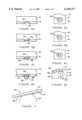
- FIG. 1is a schematic plan view of a direct die connect (DDC) die constructed in accordance with the invention
- FIG. 2is a schematic plan view of a semiconductor package constructed in accordance with the invention.
- FIG. 3is a cross sectional view taken along section line 3--3 of FIG. 2;
- FIG. 3Ais a schematic cross sectional view equivalent to FIG. 3 of an alternate embodiment semiconductor package having conductive adhesive contacts;
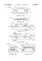
- FIG. 4is a block diagram illustrating a method for fabricating a direct die connect (DDC) die in accordance with the invention
- FIG. 5Ais a schematic cross sectional view of an electrode for the DDC die during an activating step
- FIG. 5Bis a schematic cross sectional view of the electrode illustrating deposition of an adherence layer on the electrode
- FIG. 5Cis a schematic cross sectional view of the electrode illustrating deposition of a solder wettable layer on the adherence layer;
- FIG. 5Dis a schematic cross sectional view of the electrode illustrating formation of a solder bump on the solder wettable layer
- FIG. 6Ais a schematic cross sectional view of an electroless plating tank configured to activate the electrodes
- FIG. 6Bis a schematic cross sectional view of an electroless plating tank configured to electrolessly deposit adherence layers on the electrodes;
- FIG. 6Cis a schematic cross sectional view of an electroless plating tank configured to electrolessly deposit solder wettable layers on the adherence layers;
- FIG. 6Dis a schematic cross sectional view of a wave soldering apparatus configured to deposit solder bumps on the solder wettable layers;
- FIG. 7is an enlarged schematic view of a portion of the wave soldering apparatus illustrating formation of the solder bumps on the electrolessly deposited layers;
- FIG. 8Ais an enlarged schematic plan view of a chip scale package constructed in accordance with the invention.
- FIG. 8Bis a side elevation view of FIG. 8A;
- FIG. 9Ais a schematic cross sectional view of a temporary package constructed in accordance with the invention.
- FIG. 9Bis a schematic cross sectional view of an alternate embodiment temporary package
- FIG. 10Ais an enlarged cross sectional view taken along section line 10A--10A of FIG. 9A;
- FIG. 10Bis an enlarged cross sectional view taken along section line 10B--10B of FIG. 9B;
- FIG. 11is a plan view of a multi chip module constructed in accordance with the invention.
- FIGS. 11A-Care schematic cross sectional view illustrating an assembly sequence for the multi chip module of FIG. 11;
- FIG. 11Dis an enlarged cross sectional view taken along section line 11D--11D of FIG. 11B;
- FIG. 11Eis an enlarged cross sectional view taken along section line 11E--11E of FIG. 11C;
- FIG. 12Ais a schematic diagram of a conveyor furnace suitable for performing a reflow step of the assembly sequence of FIGS. 11A--C;
- FIG. 12Bis a temperature vs. time profile of a representative reflow step.
- a direct die connect (DDC) die 10constructed in accordance with the invention includes a pattern of solder bumps 12 formed on a face of the die 10.
- the solder bumps 12are located on metal electrodes 36 embedded in a passivation layer 14 on the DDC die 10.
- a method for fabricating the solder bumps 12 using electroless deposition and wave solderingwill be hereinafter described.
- a semiconductor package 16 constructed in accordance with the inventioncomprises a housing 18 and multiple DDC dice 10.
- the housing 18includes separate die receiving channels 20, each adapted to contain a single DDC die 10.
- the die receiving channels 20include beveled sidewalls 28 (FIG. 3) to facilitate insertion of the DDC dice 10 into the die receiving channels 20.
- the semiconductor package 16is adapted for mounting to a supporting substrate 22 (FIG. 3), such as a printed circuit board or ceramic plate to form multi chip modules and other electrical components.
- the supporting substrate 22can include patterns of conductors 24 adapted for electrical communication with the DDC dice 10 and other components of the multi chip module.
- the semiconductor package 16comprises a multi chip module with multiple dice 10, the method of the invention can also be used to form a package having a single die.
- each die receiving channel 20includes electrical connectors in the form of spring contacts 26.
- the solder bumps 12 on the DDC dice 10can be bonded to the spring contacts 26 using a reflow process.
- the spring contacts 26can include a base 30 adapted for electrical communication with the conductors 24 on the supporting substrate 22.
- the base 30can be bonded to the substrate 22 using solder 32.
- the spring contacts 26can be formed of a solderable metal such as beryllium copper, or "PALLINEY 7" available from J. M. Ney Company of Hartford, Conn.
- the DDC dice 10can be inserted into the channels 20 using an insertion tool or loading mechanism (not shown). With the DDC dice 10 completely inserted into the channels 20, the solder bumps 12 electrically engage the spring contacts 26.
- the spring contacts 26can be formed to exert predetermined contact forces on the solder bumps 12. However, since the solder bumps 12 project from the passivation layer 14 on the face of the DDC dice 10, the spring contacts 26 can be formed to minimally contact the passivation layer 14 of the DDC dice 10 during insertion of the dice 10 into the channels 20. This helps to prevent damage to the passivation layer 14 and solder bumps 12 during assembly of the package 16.
- the solder bumps 12can be reflowed. This step can be performed using a "conveyor furnace" adapted to move the package 16 at a predetermined speed through different temperature zones.
- the temperature zonescan include one or more preheat zones, a reflow zone and a cool down zone.
- the reflow zonecan be maintained at a peak temperature of from 40° C. to 80° C. above the melting temperature of the solder bumps 12. This temperature can be maintained for a time period of several minutes.
- Reflowing the solder bumps 12forms bonded metal to metal connections between the solder bumps 12 and the spring contacts 26.
- the bonded connectionsprovide low resistance electrical paths and prevent movement and "fretting" of the spring contacts 26 with respect to the DDC dice 10.
- the bonded connections provided by the reflowed solder bumps 12anchor the dice 10 within the package 16, and prevent movement of the dice 10 and spring contacts 26.
- the solder bumps 12can be heated to reflow the solder, and loosen the bonded connections with the spring contacts 26. Because the spring contacts 26 can be shaped to exert minimal contact force, damage to the passivation layer 14 can be minimized during removal of the dice 10.
- the bump fabrication methodincludes the steps of:
- step AProviding a semiconductor die having metal electrodes, step A.
- step BCleaning and activating the metal electrodes for subsequent electroless deposition, step B.
- step DElectrolessly depositing solder wettable layers on the adherence layers, step D.
- step EDepositing solder bumps on the solder wettable layers using a wave soldering apparatus, step E.
- the semiconductor die 10can be provided with the patterns of electrodes 36 embedded in the passivation layer 14.
- the electrodes 36can comprise thin film aluminum bond pads in electrical communication with aluminum metallization and integrated circuits formed on the DDC die 10. Typical aluminum bond pads have a thickness of from 1.0 to 1.5 ⁇ m.
- the passivation layer 14can comprise a glass such as borophosphosilicate glass (BPSG), or phosphorous silicate glass (PSG), an oxide such as SiO 2 , or a nitride, such as Si 3 N 4 . Openings 34 (FIG. 5A) can be provided in the passivation layer 14 to allow access to the electrodes 36.
- the electrodes 36can also be formed using additional metallization and passivation layers, as described in U.S. Pat. No. 5,593,927, entitled “Method For Packaging Semiconductor Dice", incorporated herein by reference. Using the method described in the cited patent, the electrodes 36 can be formed in a desired pattern in electrical communication with a standardized pattern of bond pads. For example, a die having bond pads along its center line can be modified using the method of the '927 patent with additional passivation and metallization layers.
- the electrodes 36can be formed by depositing an additional insulating layer on the dice 10, followed by screen printing or stenciling, of additional metallization in electrical communication with the standard device bond pads. This allows the electrodes 36 to be formed in desired locations as required, such as along an edge of the die 10, to accommodate the locations of the spring contacts 26 (FIG. 3).
- the die 10in order to clean and activate the electrodes 36 for subsequent electroless deposition, the die 10 can be submerged in an activation bath 38.
- the activation bath 38contains an activation solution 40 at a temperature of from 20° C. to 40° C.
- the activation solution 40functions to strip native oxide layers present on the electrodes 36.
- One suitable activation solutionincludes a zincate, such as ZnO 2 or Zn(OH 4 ).
- Zincate solutionsare commercially available from Lea Ronal, as well as other manufacturers.
- adhesion metal layers 42can be formed on the electrodes 36.
- Preferred materials for the adhesion metal layers 42include Ni, Zn, Cr, Au, and Pd.
- An adhesion bath 44 (FIG. 6B) containing an adhesion metal solution 46can be used to electrolessly deposit the adhesion metal layers 42 through the openings 34 in the passivation layer 14 onto the electrodes 36.
- a suitable adhesion metal solution 46can include nickel chloride, sodium hydroxyacetate, and sodium hypophosphate at a temperature of about 85° to 90° C.
- a representative thickness for the adhesion metal layers 42can be from 500 ⁇ to 10 ⁇ m. This thickness can be achieved by controlling the concentration of the adhesion metal solution 46 and the time period during which the die 10 is submerged.
- a representative time period for submergencecan be from 1 to 5 minutes.
- solder wettable layers 48can be formed on the adhesion metal layers 42.
- Preferred metals for the solder wettable layers 48include palladium and gold.
- a solder wettable bath 50 containing a solder wettable solution 52can be used to electrolessly deposit the solder wettable layers 48 onto the adhesion metal layers 42.
- a suitable solder wettable solution 52includes palladium chloride and sodium hypophosphate at a temperature of about 50° to 60° C.
- a representative thickness for the solder wettable layers 48can be from 500 ⁇ to 0.1 ⁇ m. This thickness can be achieved by controlling the concentration of the solder wettable solution 52 and the time period for which the die 10 is submerged.
- a representative time period for a 1 gm/liter solution of palladium chloride and sodium hypophosphatecan be from 1 to 2 minutes.
- the solder bumps 12can be deposited on the solder wettable layers 48 using a wave soldering apparatus 54.
- the wave soldering apparatus 54can include a tank with molten solder 56 formulated as required. Suitable formulations include 95%Pb/5%Sn, 60% Pb/40%Sn, 63%In/37%Sn, 100%Sn, 62%Pb/36% Sn/2%Au. A representative temperature for the molten solder 56 can be from 180° C. to 260° C.
- the wave soldering apparatus 54can also include a pump 58 and baffles 60 configured to produce a turbulent solder wave 64.
- a conveyor 66can be used to move the die 10 past the solder wave 64.
- a heater element 62can be used to preheat the die 10 prior to exposure to the solder wave 64.
- One suitable wave soldering apparatus 54is available from Electrovat of Montreal, Canada and is designated a model no. 605C.
- the solder bumps 12deposit onto the electrodes 36, as the die 10 is moved proximate to the solder wave 64.
- the solder wettable layers 48(FIG. 5C) on the electrodes 36 provide surfaces for attracting solder and building the solder bumps 12.
- the solderis attracted to the surfaces of the wettable layers 48.
- the processis self aligning in that only the exposed surfaces of the solder wettable layers 48 are plated with solder. With some materials the solder wettable layers 48 will be partially or totally consumed by reaction with the solder.
- palladiumcombines with solder so that the deposited solder bumps 12 can include microscopic spheres of pure palladium embedded in a Pb--Sn matrix.
- the solder bumps 12can be generally hemispherical in shape, with generally convex sidewalls 70 and a rounded tip portion 68.
- a representative height of the solder bumps 12can be from 1 mils to 5 mils.
- a diameter of the solder bumps 12can be determined by the bond pad size and geometry of the electrodes 36 (FIG. 5A) with 2 to 20 mils being representative.
- the geometry of the solder bumps 12can also be controlled by the orientation of the die 10 with respect to the solder wave 64, by the temperature of the solder wave 64 (e.g., above, below, angle etc.), and by the speed of the conveyor 66. In general, increased temperatures and higher speeds of the conveyor 66 produce taller solder bumps 12.
- an alternate embodiment semiconductor package 16Aincludes DDC dice 10A having conductive adhesive bumps 12A.
- One type of conductive adhesive suitable for forming the conductive adhesive bumps 12Acomprises a "z-axis anisotropic adhesive". Z-axis anisotropic adhesives are filled with conductive particles to a low level such that the particles do not contact each other in the xy plane. Compression of the material in the z direction establishes an electrical path.
- Z-axis anisotropic adhesivescan be formed as a viscous paste, or as a film that is applied and then cured to harden. Both types of z-axis anisotropic adhesives (paste or film) come in a thermal plastic or thermal setting variety. Thermal plastic anisotropic adhesives are heated to soften for use and then cooled for curing. Thermal setting anisotropic adhesives require heat curing at temperatures from 100-300° C. for from several minutes to an hour or more. Suitable z-axis anisotropic adhesives are sold under the trademarks: "X-POLY” and "Z-POXY", by A.I. Technology, Trenton, N.J.; and "SHELL-ZAC", by Sheldahl, Northfield, Minn.
- Z-axis anisotropic adhesivesare also sold by 3M, St. Paul, Minn.
- the conductive adhesive materialcan be applied to the bond pads of a conventional semiconductor die to form the conductive adhesive bumps 12A.
- electrodes equivalent to the electrodes 36 (FIG. 5A) previously describedcan be fabricated in desired configuration using the previously cited '927 patent.
- the conductive adhesive bumps 12A in addition to forming electrically conductive paths to the spring contacts 26can also provide a compliant member for contact with the spring contacts 26. In particular some conductive adhesive formulations possess resilient characteristics.
- the conductive adhesive bumps 12Acan be formed with a height that allows the spring contacts 26 to minimally contact the passivation layer 14A of the DDC dice 10A during insertion of the dice 10A into the die receiving channels 20. The size and diameters of the conductive adhesive bumps 12A can be as previously explained for the solder bumps 12.
- the conductive adhesive bumps 12Acan also be configured to form bonded connections to the spring contacts 26.
- the conductive adhesive bumps 12Acan be in a semi-cured, or B-stage condition, during insertion of the DDC dice 10A into the channels 28. Complete curing of the conductive adhesive bumps 12A can be performed after the bumps 12A have been placed into contact with the spring contacts 26. The spring contacts 26 can thus apply a compressive force to the conductive adhesive bumps 12A during curing.
- a DDC die 10B having solder bumps 12B fabricated substantially as previously described for die 10(FIG. 1) is illustrated.
- the DDC die 10Bcan be used to fabricate a chip scale package 16B.
- the chip scale package 16Bincludes a fan out substrate 72 to which the DDC die 10B can be flip chip bonded.
- the fan out substrate 72can be formed of an electrically insulating material such as ceramic or FR-4.
- the fan out substrate 72can include patterns of conductors 74 formed on a first surface (face) thereof in electrical communication with ball contacts 76 on an opposing surface (back side) thereof.
- the ball contacts 76can be arranged in a dense array such as a ball grid array (BGA). Alternately in place of ball contacts 76 in a BGA, other dense configurations of external contacts such as pins in a pin grid array (PGA), or pads in a land grid array (LGA) can be used.
- BGAball grid array
- PGApin grid array
- LGAland grid array
- solder bumps 12Bcan be aligned and bonded to bonding sites on the conductors 74 using an aligner bonder tool or other techniques known in the art.
- a suitable aligner bonder toolis manufactured by Research Devices, Inc. of Piscataway, N.J.
- solder bumps 12Ccan be fabricated substantially as previously described on an interconnect 78A for a temporary package 16C.
- the interconnect 78Acan include contact members 80 adapted to establish temporary electrical communication with contact locations 82 (e.g., bond pads) on a semiconductor die 84 for testing.
- the interconnect 78Acan be fabricated substantially as described in U.S. Pat. No. 5,483,741, entitled “Method For Fabricating A Self Limiting Silicon Based Interconnect For Testing Bare Semiconductor Dice", incorporated herein by reference.
- the temporary package 16Ccan be fabricated substantially as described in U.S. Pat. No. 5,519,332, entitled “Carrier For Testing An Unpackaged Semiconductor Die", incorporated herein by reference.
- the interconnect 78Acan include patterns of conductors 86 in electrical communication with the contact members 80.
- the solder bumps 12Ccan be formed on bonding sites on the conductors 86 using electroless deposition and wave soldering as previously described for solder bumps 12 (FIG. 5D).
- the temporary package 16Ccan include electrical connectors 88 in electrical communication with test circuitry 90.
- the electrical connectors 88can be metal tines, or laminated conductors formed on a multi layered tape similar to TAB tape.
- the solder bumps 12Ccan be bonded to the electrical connectors 88 using a reflow process substantially as previously described for solder bumps 12. The bonded connections provided by the solder bumps 12C provide low resistance electrical paths for high speed testing of the die 84.
- an interconnect 78Bincludes solder bumps 12D fabricated using electroless deposition and wave soldering as previously described.
- the interconnect 78Bcan be a component of a temporary package 16D adapted to test semiconductor dice 84B having raised contact locations 82B (e.g., bumped bond pads).
- the interconnect 78B and temporary package 16Dcan be fabricated substantially as described in U.S. patent application Ser. No. 08/818,456 entitled "Direct Connect Interconnect For Testing Semiconductor Dice And Wafers", incorporated herein by reference.
- the solder bumps 12Dcan be bonded to electrical connectors 88B on the temporary package 16D in electrical communication with test circuitry 90B.
- a multi chip module 92 constructed in accordance with the inventionincludes multiple DDC dice 10M and a supporting substrate 94.
- the DDC dice 10Minclude solder bumps 12M (FIG. 12M) and pads 102 (FIG. 12M) fabricated using electroless deposition and wave soldering, substantially as previously described.
- the supporting substrate 94includes bumped electrodes 96 (FIG. 11A) and pads 108 fabricated using electroless deposition and wave soldering, substantially as previously described.
- the bumped electrodes 96 (FIG. 11A)are fabricated in patterns that match the patterns of the solder bumps 12M (FIG. 11A) on the DDC dice 10M.
- the bumped electrodes 96 and solder bumps 12Mcan be formed of the solder alloys previously described. However, preferably the bumped electrodes 96 and the solder bumps 12M comprise different solder alloys having different melting temperatures.
- one of the solder alloyscan be a high temperature alloy, such as 95%Pb/5%Sn, and the other solder alloy a low temperature eutectic alloy, such as 63%Pb/37%Sn.
- Some low temperature soldershave a melting temperature of about 180° C.-190° C.
- some high temperature soldershave a melting temperature of about 260° C.-280° C.
- the different melting temperaturesaid in the subsequent assembly of the multi chip module 94.
- the solder bumps 12Mare formed of a high temperature solder alloy
- the bumped electrodes 96are formed of a low temperature solder alloy.
- the supporting substrate 94can be formed of a rigid material such as silicon, ceramic or FR-4.
- the supporting substrate 94can include an alignment member 98 (FIG. 11A).
- the alignment member 98can comprise a plate formed separately of a material, such as silicon, ceramic, or FR-4, and then attached to the supporting substrate 94.
- the alignment membercan comprise a deposited, patterned and cured polymer.
- the alignment member 98comprises a patterned and cured layer of resist.
- One suitable resist for forming the alignment member 98comprises a negative tone resist, blanket deposited to a desired thickness, exposed, developed and then cured.
- a suitable resist formulationis sold by Shell Chemical under the trademark "EPON RESIN SU-8". Such a resist can be deposited to a thickness of from about 5-50 mils.
- a conventional resist coating apparatussuch as a spin coater, can be used to deposit the resist onto the supporting substrate 94. The deposited resist can then be "prebaked" at about 95° C. for about 15 minutes and exposed in a desired pattern using a conventional UV aligner with a dose of about 165 mJ/cm 2 .
- Developingcan be accomplished with a solution of PGMEA (propylenglycol-monomethylether-acetate). This can be followed by a hard bake at about 200° C. for about 30 minutes.
- the alignment member 98includes patterns of alignment openings 104.
- Each alignment opening 104is sized and shaped to contact the peripheral edges of a DDC die 10M. This aligns the DDC dice 10M on the substrate 94, and provides alignment of the contact bumps 12M to the bumped electrodes 96. Alternately alignment can be performed using a vision alignment system such as an aligner-bonder used for flip chip bonding conventional semiconductor dice to circuit boards.
- One suitable aligner bonderis sold by Research Devices Inc. of Piscataway, N.J.
- FIG. 11Bthe DDC die 10M has been aligned by the alignment member 98 so that the solder bumps 12M are in physical contact with the bumped electrodes 96.
- FIG. 11Dis an enlarged view showing the physical contact between the contact bumps 12M and the bumped electrodes 96.
- the solder bumps 12M and bumped electrodes 96can be reflowed to form bonded connections 106.
- the solder bumps 12Mcan be formed of a high melting temperature alloy whereas the bumped electrodes 96 can be formed of a low melting temperature alloy. Accordingly, the temperature of the reflow process can be maintained at a temperature between the different melting temperatures. This allows the solder bumps 12M to soften but not enter the liquid phase.
- the softened solder bumps 12Mhave a structural rigidity that prevents collapse of the die 10M onto the supporting substrate 94.
- the bumped electrodes 96liquefy and flow into the solder bumps 12M to form the bonded connections 106 (FIG. 11E).
- This processis self aligning in that the liquidified bumped electrodes 96 are attracted to the softened solder bumps 12M.
- the bonded connections 106cool and harden into a rigid solder joint.
- a conveyorized furnace 110which can be used to perform the reflow-bonding process, is shown.
- the conveyorized furnace 110includes a conveyor 112 adapted to move the DDC die 10M and supporting substrate 94 assembled as shown in FIG. 11B through four different temperature zones 1-4.
- Zones 1 and 2can be maintained at pre-heat temperatures (e.g., 0-150° C.).
- Zone 3can be maintained at a temperature above the melting point of the bumped electrodes 96, but below the melting point of the solder bumps 12M (e.g., 180° C. to 260° C.).
- Zone 4can be maintained at a cool-down temperature (e.g., 50° C. to 100° C.).
- the conveyorized furnace 110can be configured so that the preheating occurs in the first three minutes, reflowing occurs during the next four minutes, and cooling occurs during the final three minutes.
- the illustrative embodimentis with a conveyorized furnace, the reflow process can also be performed using a heated vapor phase reflow process.
- the method of the inventioncan be employed to fabricate other types of package.
- Another package that can include solder bumps formed in accordance with the inventionis described in U.S. patent application Ser. No. 08/563,191, entitled “Method Of Producing A Single Piece Package For Semiconductor Die", incorporated herein by reference.
- the inventionprovides improved semiconductor packages and methods for fabricating solder bumps for semiconductor dice, packages and interconnects.
- the methodis characterized by low temperatures and simple process steps.
- masks and stencilsare not required for locating the solder bumps.
Landscapes
- Engineering & Computer Science (AREA)
- Computer Hardware Design (AREA)
- Microelectronics & Electronic Packaging (AREA)
- Power Engineering (AREA)
- Manufacturing & Machinery (AREA)
- Wire Bonding (AREA)
Abstract
Description
Claims (19)
Priority Applications (1)
| Application Number | Priority Date | Filing Date | Title |
|---|---|---|---|
| US09/098,197US6150717A (en) | 1997-08-04 | 1998-06-16 | Direct die contact (DDC) semiconductor package |
Applications Claiming Priority (2)
| Application Number | Priority Date | Filing Date | Title |
|---|---|---|---|
| US08/905,602US6107122A (en) | 1997-08-04 | 1997-08-04 | Direct die contact (DDC) semiconductor package |
| US09/098,197US6150717A (en) | 1997-08-04 | 1998-06-16 | Direct die contact (DDC) semiconductor package |
Related Parent Applications (1)
| Application Number | Title | Priority Date | Filing Date |
|---|---|---|---|
| US08/905,602DivisionUS6107122A (en) | 1997-08-04 | 1997-08-04 | Direct die contact (DDC) semiconductor package |
Publications (1)
| Publication Number | Publication Date |
|---|---|
| US6150717Atrue US6150717A (en) | 2000-11-21 |
Family
ID=25421123
Family Applications (2)
| Application Number | Title | Priority Date | Filing Date |
|---|---|---|---|
| US08/905,602Expired - LifetimeUS6107122A (en) | 1997-08-04 | 1997-08-04 | Direct die contact (DDC) semiconductor package |
| US09/098,197Expired - LifetimeUS6150717A (en) | 1997-08-04 | 1998-06-16 | Direct die contact (DDC) semiconductor package |
Family Applications Before (1)
| Application Number | Title | Priority Date | Filing Date |
|---|---|---|---|
| US08/905,602Expired - LifetimeUS6107122A (en) | 1997-08-04 | 1997-08-04 | Direct die contact (DDC) semiconductor package |
Country Status (1)
| Country | Link |
|---|---|
| US (2) | US6107122A (en) |
Cited By (81)
| Publication number | Priority date | Publication date | Assignee | Title |
|---|---|---|---|---|
| US6364196B1 (en) | 1998-08-28 | 2002-04-02 | Micron Technology, Inc. | Method and apparatus for aligning and attaching balls to a substrate |
| US20020140077A1 (en)* | 1998-02-27 | 2002-10-03 | Micron Technology, Inc. | Multichip semiconductor package |
| US6492738B2 (en)* | 1999-09-02 | 2002-12-10 | Micron Technology, Inc. | Apparatus and methods of testing and assembling bumped devices using an anisotropically conductive layer |
| US20020187626A1 (en)* | 1998-03-30 | 2002-12-12 | Kinsman Larry D. | Vertical surface mount assembly and methods |
| US20030042581A1 (en)* | 2001-08-29 | 2003-03-06 | Fee Setho Sing | Packaged microelectronic devices and methods of forming same |
| US6541848B2 (en)* | 1998-02-25 | 2003-04-01 | Fujitsu Limited | Semiconductor device including stud bumps as external connection terminals |
| US6548376B2 (en) | 2001-08-30 | 2003-04-15 | Micron Technology, Inc. | Methods of thinning microelectronic workpieces |
| US6558600B1 (en) | 2000-05-04 | 2003-05-06 | Micron Technology, Inc. | Method for packaging microelectronic substrates |
| US20030090884A1 (en)* | 2001-11-15 | 2003-05-15 | Sang-Do Lee | Wafer-level chip scale package having stud bump and method for fabricating the same |
| US6564979B2 (en) | 2001-07-18 | 2003-05-20 | Micron Technology, Inc. | Method and apparatus for dispensing adhesive on microelectronic substrate supports |
| US6576494B1 (en) | 2000-06-28 | 2003-06-10 | Micron Technology, Inc. | Recessed encapsulated microelectronic devices and methods for formation |
| US6622380B1 (en) | 2002-02-12 | 2003-09-23 | Micron Technology, Inc. | Methods for manufacturing microelectronic devices and methods for mounting microelectronic packages to circuit boards |
| US20030190843A1 (en)* | 1998-05-04 | 2003-10-09 | Farnworth Warren M. | Apparatus for forming modular sockets using flexible interconnects and resulting structures |
| US6638595B2 (en) | 2000-06-28 | 2003-10-28 | Micron Technology, Inc. | Method and apparatus for reduced flash encapsulation of microelectronic devices |
| US6653173B2 (en) | 2000-06-16 | 2003-11-25 | Micron Technology, Inc. | Method and apparatus for packaging a microelectronic die |
| US6656769B2 (en) | 2000-05-08 | 2003-12-02 | Micron Technology, Inc. | Method and apparatus for distributing mold material in a mold for packaging microelectronic devices |
| US20040029425A1 (en)* | 2002-08-06 | 2004-02-12 | Yean Tay Wuu | Temporary, conformable contacts for microelectronic components |
| US20040026776A1 (en)* | 2002-08-08 | 2004-02-12 | Brand Joseph M. | Microelectronic devices and methods for manufacturing and operating packaged microelectronic device assemblies |
| US20040031621A1 (en)* | 2002-08-19 | 2004-02-19 | Heng Puah Kia | Packaged microelectronic component assemblies |
| US20040035917A1 (en)* | 2002-08-22 | 2004-02-26 | Michel Koopmans | Apparatus and method for depositing and reflowing solder paste on a microelectronic workpiece |
| US20040038447A1 (en)* | 2002-08-21 | 2004-02-26 | Corisis David J | Packaged microelectronic devices and methods for assembling microelectronic devices |
| US20040036490A1 (en)* | 2002-08-26 | 2004-02-26 | Ralph Schaeffer | Selectively configurable probe structures, e.g., for testing microelectronic components |
| US20040042190A1 (en)* | 2002-08-27 | 2004-03-04 | Eng Meow Koon | Multiple chip semiconductor package and method of fabricating same |
| US20040041260A1 (en)* | 2002-08-29 | 2004-03-04 | Wood Alan G. | Semiconductor component with backside contacts and method of fabrication |
| US20040040149A1 (en)* | 2002-08-29 | 2004-03-04 | Wood Alan G. | Probe card , e.g., for testing microelectronic components, and methods for making same |
| US6717245B1 (en)* | 2000-06-02 | 2004-04-06 | Micron Technology, Inc. | Chip scale packages performed by wafer level processing |
| US20040121563A1 (en)* | 2002-03-06 | 2004-06-24 | Farnworth Warren M. | Method for fabricating encapsulated semiconductor components having conductive vias |
| US20040159946A1 (en)* | 2001-12-26 | 2004-08-19 | Stephen Moxham | Microelectronic assemblies, electronic devices, and apparatuses for supporting microelectronic substrates |
| US20040173899A1 (en)* | 2003-03-04 | 2004-09-09 | Peng Neo Chee | Microelectronic component assemblies employing lead frames having reduced-thickness inner lengths |
| US20040178495A1 (en)* | 2003-03-14 | 2004-09-16 | Yean Tay Wuu | Microelectronic devices and methods for packaging microelectronic devices |
| US20040179931A1 (en)* | 1999-10-19 | 2004-09-16 | Peterson Darin L. | Methods and apparatus for retaining a tray stack having a plurality of trays for carrying microelectronic devices |
| US6798667B2 (en)* | 2002-08-23 | 2004-09-28 | Ati Technologies, Inc. | Solder ball collapse control apparatus and method thereof |
| US6796028B2 (en) | 2000-08-23 | 2004-09-28 | Micron Technology, Inc. | Method of Interconnecting substrates for electrical coupling of microelectronic components |
| US20040191955A1 (en)* | 2002-11-15 | 2004-09-30 | Rajeev Joshi | Wafer-level chip scale package and method for fabricating and using the same |
| US20040200522A1 (en)* | 2003-03-17 | 2004-10-14 | Kyocera Corporation | Solar cell element and solar cell module |
| US20040219887A1 (en)* | 1999-12-06 | 2004-11-04 | Conexant Systems, Inc. | Surface acoustic wave filter packaging |
| US6836009B2 (en) | 2002-08-08 | 2004-12-28 | Micron Technology, Inc. | Packaged microelectronic components |
| US6838760B1 (en) | 2000-08-28 | 2005-01-04 | Micron Technology, Inc. | Packaged microelectronic devices with interconnecting units |
| US20050012225A1 (en)* | 2002-11-15 | 2005-01-20 | Choi Seung-Yong | Wafer-level chip scale package and method for fabricating and using the same |
| US20050019988A1 (en)* | 2002-04-04 | 2005-01-27 | Tongbi Jiang | Method and apparatus for attaching microelectronic substrates and support members |
| WO2005010976A1 (en)* | 2003-07-21 | 2005-02-03 | Xilinx, Inc. | A programmable multi-chip module |
| US20050023572A1 (en)* | 2002-08-29 | 2005-02-03 | Micron Technology, Inc. | Electronic device package |
| US20050046431A1 (en)* | 2003-09-03 | 2005-03-03 | Kirby Kyle K. | Probe card for use with microelectronic components,and methods for making same |
| US20050074955A1 (en)* | 2003-10-03 | 2005-04-07 | Vahid Goudarzi | Method and arrangement for reduced thermal stress between substrates |
| US6879050B2 (en) | 2003-02-11 | 2005-04-12 | Micron Technology, Inc. | Packaged microelectronic devices and methods for packaging microelectronic devices |
| US20050093174A1 (en)* | 2003-10-31 | 2005-05-05 | Seng Eric T.S. | Reduced footprint packaged microelectronic components and methods for manufacturing such microelectronic components |
| US20050104228A1 (en)* | 2003-11-13 | 2005-05-19 | Rigg Sidney B. | Microelectronic devices, methods for forming vias in microelectronic devices, and methods for packaging microelectronic devices |
| US20050104171A1 (en)* | 2003-11-13 | 2005-05-19 | Benson Peter A. | Microelectronic devices having conductive complementary structures and methods of manufacturing microelectronic devices having conductive complementary structures |
| US20050134299A1 (en)* | 2003-12-22 | 2005-06-23 | Cram Daniel P. | System and apparatus for testing packaged devices and related methods |
| US6921860B2 (en) | 2003-03-18 | 2005-07-26 | Micron Technology, Inc. | Microelectronic component assemblies having exposed contacts |
| US20050176233A1 (en)* | 2002-11-15 | 2005-08-11 | Rajeev Joshi | Wafer-level chip scale package and method for fabricating and using the same |
| US20050206401A1 (en)* | 2004-03-22 | 2005-09-22 | Caldwell John L | Test sockets, test systems, and methods for testing microfeature devices |
| US6951982B2 (en) | 2002-11-22 | 2005-10-04 | Micron Technology, Inc. | Packaged microelectronic component assemblies |
| US20050277279A1 (en)* | 2004-06-14 | 2005-12-15 | Shijian Luo | Microfeature devices and methods for manufacturing microfeature devices |
| US6979595B1 (en) | 2000-08-24 | 2005-12-27 | Micron Technology, Inc. | Packaged microelectronic devices with pressure release elements and methods for manufacturing and using such packaged microelectronic devices |
| US20060040428A1 (en)* | 2004-08-19 | 2006-02-23 | Johnson Mark S | Conductive structures for microfeature devices and methods for fabricating microfeature devices |
| US20060046346A1 (en)* | 2004-09-01 | 2006-03-02 | Benson Peter A | Methods for packaging microfeature devices and microfeature devices formed by such methods |
| US20060043611A1 (en)* | 2004-09-01 | 2006-03-02 | Kinsman Larry D | Reduced-dimension microelectronic component assemblies with wire bonds and methods of making same |
| US20060180639A1 (en)* | 2005-02-16 | 2006-08-17 | Motorola, Inc. | Method and arrangement for thermally relieved packages with different substrates |
| US20060208366A1 (en)* | 2004-07-23 | 2006-09-21 | Micron Technology, Inc. | Microelectronic component assemblies with recessed wire bonds and methods of making same |
| US20060292858A1 (en)* | 2002-07-18 | 2006-12-28 | Micron Technology, Inc. | Techniques to create low K ILD for beol |
| US20070045797A1 (en)* | 2005-08-24 | 2007-03-01 | Micron Technology, Inc. | Microelectronic devices and microelectronic support devices, and associated assemblies and methods |
| US20070045872A1 (en)* | 2005-08-31 | 2007-03-01 | Fee Setho S | Microelectronic devices having intermediate contacts for connection to interposer substrates, and associated methods of packaging microelectronic devices with intermediate contacts |
| US7259451B2 (en) | 2003-08-29 | 2007-08-21 | Micron Technology, Inc. | Invertible microfeature device packages |
| US7273769B1 (en) | 2000-08-16 | 2007-09-25 | Micron Technology, Inc. | Method and apparatus for removing encapsulating material from a packaged microelectronic device |
| US20070228577A1 (en)* | 2006-03-29 | 2007-10-04 | Micron Technology, Inc. | Packaged microelectronic devices recessed in support member cavities, and associated methods |
| US20080012110A1 (en)* | 2006-07-17 | 2008-01-17 | Micron Technology, Inc. | Microelectronic packages with leadframes, including leadframes configured for stacked die packages, and associated systems and methods |
| US20080224329A1 (en)* | 2007-03-13 | 2008-09-18 | Micron Technology, Inc. | Packaged microelectronic devices and methods for manufacturing packaged microelectronic devices |
| US7518237B2 (en) | 2005-02-08 | 2009-04-14 | Micron Technology, Inc. | Microfeature systems including adhered microfeature workpieces and support members |
| US20090273359A1 (en)* | 2008-05-02 | 2009-11-05 | Micron Technology, Inc. | Electrical testing apparatus having masked sockets and associated systems and methods |
| US7622377B2 (en) | 2005-09-01 | 2009-11-24 | Micron Technology, Inc. | Microfeature workpiece substrates having through-substrate vias, and associated methods of formation |
| US7671459B2 (en) | 2006-02-08 | 2010-03-02 | Micron Technologies, Inc. | Microelectronic devices, stacked microelectronic devices, and methods for manufacturing such devices |
| US20100154190A1 (en)* | 2008-12-19 | 2010-06-24 | Sanger Kurt M | Method of making a composite device |
| US7759221B2 (en) | 2005-12-29 | 2010-07-20 | Micron Technology, Inc. | Methods for packaging microelectronic devices and microelectronic devices formed using such methods |
| US7807505B2 (en) | 2005-08-30 | 2010-10-05 | Micron Technology, Inc. | Methods for wafer-level packaging of microfeature devices and microfeature devices formed using such methods |
| US7833456B2 (en) | 2007-02-23 | 2010-11-16 | Micron Technology, Inc. | Systems and methods for compressing an encapsulant adjacent a semiconductor workpiece |
| US7843050B2 (en) | 2007-07-24 | 2010-11-30 | Micron Technology, Inc. | Microelectronic die packages with metal leads, including metal leads for stacked die packages, and associated systems and methods |
| US7910385B2 (en) | 2006-05-12 | 2011-03-22 | Micron Technology, Inc. | Method of fabricating microelectronic devices |
| US7947529B2 (en) | 2007-08-16 | 2011-05-24 | Micron Technology, Inc. | Microelectronic die packages with leadframes, including leadframe-based interposer for stacked die packages, and associated systems and methods |
| US20110198745A1 (en)* | 2010-02-17 | 2011-08-18 | Maxim Integrated Products, Inc. | Wafer-level packaged device having self-assembled resilient leads |
| US8084866B2 (en) | 2003-12-10 | 2011-12-27 | Micron Technology, Inc. | Microelectronic devices and methods for filling vias in microelectronic devices |
Families Citing this family (21)
| Publication number | Priority date | Publication date | Assignee | Title |
|---|---|---|---|---|
| US6740960B1 (en)* | 1997-10-31 | 2004-05-25 | Micron Technology, Inc. | Semiconductor package including flex circuit, interconnects and dense array external contacts |
| US6097087A (en) | 1997-10-31 | 2000-08-01 | Micron Technology, Inc. | Semiconductor package including flex circuit, interconnects and dense array external contacts |
| US6765652B1 (en)* | 1998-01-12 | 2004-07-20 | Micron Technology, Inc. | Forming thermally curable materials on a support structure in an electronic device |
| US6259036B1 (en) | 1998-04-13 | 2001-07-10 | Micron Technology, Inc. | Method for fabricating electronic assemblies using semi-cured conductive elastomeric bumps |
| JPH11312711A (en)* | 1998-04-30 | 1999-11-09 | Murata Mfg Co Ltd | Method for connecting electronic component |
| US6297542B1 (en)* | 1998-06-25 | 2001-10-02 | Micron Technology, Inc. | Connecting a die in an integrated circuit module |
| US6320253B1 (en)* | 1998-09-01 | 2001-11-20 | Micron Technology, Inc. | Semiconductor device comprising a socket and method for forming same |
| US6263566B1 (en)* | 1999-05-03 | 2001-07-24 | Micron Technology, Inc. | Flexible semiconductor interconnect fabricated by backslide thinning |
| US20020016070A1 (en)* | 2000-04-05 | 2002-02-07 | Gerald Friese | Power pads for application of high current per bond pad in silicon technology |
| US6724078B1 (en)* | 2000-08-31 | 2004-04-20 | Intel Corporation | Electronic assembly comprising solderable thermal interface |
| US6582990B2 (en)* | 2001-08-24 | 2003-06-24 | International Rectifier Corporation | Wafer level underfill and interconnect process |
| US6673649B1 (en)* | 2002-07-05 | 2004-01-06 | Micron Technology, Inc. | Microelectronic device packages and methods for controlling the disposition of non-conductive materials in such packages |
| US7182241B2 (en)* | 2002-08-09 | 2007-02-27 | Micron Technology, Inc. | Multi-functional solder and articles made therewith, such as microelectronic components |
| US7071421B2 (en) | 2003-08-29 | 2006-07-04 | Micron Technology, Inc. | Stacked microfeature devices and associated methods |
| US20070045812A1 (en)* | 2005-08-31 | 2007-03-01 | Micron Technology, Inc. | Microfeature assemblies including interconnect structures and methods for forming such interconnect structures |
| US20070148820A1 (en)* | 2005-12-22 | 2007-06-28 | Micron Technology, Inc. | Microelectronic devices and methods for manufacturing microelectronic devices |
| US7749882B2 (en)* | 2006-08-23 | 2010-07-06 | Micron Technology, Inc. | Packaged microelectronic devices and methods for manufacturing packaged microelectronic devices |
| US7868440B2 (en) | 2006-08-25 | 2011-01-11 | Micron Technology, Inc. | Packaged microdevices and methods for manufacturing packaged microdevices |
| US20130256913A1 (en)* | 2012-03-30 | 2013-10-03 | Bryan Black | Die stacking with coupled electrical interconnects to align proximity interconnects |
| US9365749B2 (en) | 2013-05-31 | 2016-06-14 | Sunray Scientific, Llc | Anisotropic conductive adhesive with reduced migration |
| US9777197B2 (en) | 2013-10-23 | 2017-10-03 | Sunray Scientific, Llc | UV-curable anisotropic conductive adhesive |
Citations (42)
| Publication number | Priority date | Publication date | Assignee | Title |
|---|---|---|---|---|
| US3809625A (en)* | 1972-08-15 | 1974-05-07 | Gen Motors Corp | Method of making contact bumps on flip-chips |
| US4188417A (en)* | 1977-05-04 | 1980-02-12 | Balzers Patent-und Beteiligungs-Aktiegesellschaft | Method of applying a dielectric layer to a substrate and a mask-forming coating for the application of a dielectric layer |
| US4316208A (en)* | 1977-06-17 | 1982-02-16 | Matsushita Electric Industrial Company, Limited | Light-emitting semiconductor device and method of fabricating same |
| US4661375A (en)* | 1985-04-22 | 1987-04-28 | At&T Technologies, Inc. | Method for increasing the height of solder bumps |
| US4927505A (en)* | 1988-07-05 | 1990-05-22 | Motorola Inc. | Metallization scheme providing adhesion and barrier properties |
| US4970571A (en)* | 1987-09-24 | 1990-11-13 | Kabushiki Kaisha Toshiba | Bump and method of manufacturing the same |
| US5104324A (en)* | 1991-06-26 | 1992-04-14 | Amp Incorporated | Multichip module connector |
| US5118027A (en)* | 1991-04-24 | 1992-06-02 | International Business Machines Corporation | Method of aligning and mounting solder balls to a substrate |
| US5140405A (en)* | 1990-08-30 | 1992-08-18 | Micron Technology, Inc. | Semiconductor assembly utilizing elastomeric single axis conductive interconnect |
| US5169680A (en)* | 1987-05-07 | 1992-12-08 | Intel Corporation | Electroless deposition for IC fabrication |
| US5207598A (en)* | 1992-02-24 | 1993-05-04 | Molex Incorporated | Edge card connector |
| US5259793A (en)* | 1992-04-06 | 1993-11-09 | Molex Incorporated | Edge connector for a printed circuit board |
| US5269453A (en)* | 1992-04-02 | 1993-12-14 | Motorola, Inc. | Low temperature method for forming solder bump interconnections to a plated circuit trace |
| US5308796A (en)* | 1991-09-30 | 1994-05-03 | At&T Bell Laboratories | Fabrication of electronic devices by electroless plating of copper onto a metal silicide |
| US5341564A (en)* | 1992-03-24 | 1994-08-30 | Unisys Corporation | Method of fabricating integrated circuit module |
| US5367196A (en)* | 1992-09-17 | 1994-11-22 | Olin Corporation | Molded plastic semiconductor package including an aluminum alloy heat spreader |
| US5461261A (en)* | 1992-05-06 | 1995-10-24 | Sumitomo Electric Industries, Ltd. | Semiconductor device with bumps |
| US5483741A (en)* | 1993-09-03 | 1996-01-16 | Micron Technology, Inc. | Method for fabricating a self limiting silicon based interconnect for testing bare semiconductor dice |
| US5519332A (en)* | 1991-06-04 | 1996-05-21 | Micron Technology, Inc. | Carrier for testing an unpackaged semiconductor die |
| US5532612A (en)* | 1994-07-19 | 1996-07-02 | Liang; Louis H. | Methods and apparatus for test and burn-in of integrated circuit devices |
| US5531942A (en)* | 1994-06-16 | 1996-07-02 | Fry's Metals, Inc. | Method of making electroconductive adhesive particles for Z-axis application |
| US5531021A (en)* | 1994-12-30 | 1996-07-02 | Intel Corporation | Method of making solder shape array package |
| US5541525A (en)* | 1991-06-04 | 1996-07-30 | Micron Technology, Inc. | Carrier for testing an unpackaged semiconductor die |
| US5547740A (en)* | 1995-03-23 | 1996-08-20 | Delco Electronics Corporation | Solderable contacts for flip chip integrated circuit devices |
| US5559444A (en)* | 1991-06-04 | 1996-09-24 | Micron Technology, Inc. | Method and apparatus for testing unpackaged semiconductor dice |
| US5578527A (en)* | 1995-06-23 | 1996-11-26 | Industrial Technology Research Institute | Connection construction and method of manufacturing the same |
| US5578526A (en)* | 1992-03-06 | 1996-11-26 | Micron Technology, Inc. | Method for forming a multi chip module (MCM) |
| US5593927A (en)* | 1993-10-14 | 1997-01-14 | Micron Technology, Inc. | Method for packaging semiconductor dice |
| US5592736A (en)* | 1993-09-03 | 1997-01-14 | Micron Technology, Inc. | Fabricating an interconnect for testing unpackaged semiconductor dice having raised bond pads |
| US5633122A (en)* | 1993-08-16 | 1997-05-27 | Micron Technology, Inc. | Test fixture and method for producing a test fixture for testing unpackaged semiconductor die |
| US5661042A (en)* | 1995-08-28 | 1997-08-26 | Motorola, Inc. | Process for electrically connecting electrical devices using a conductive anisotropic material |
| US5668059A (en)* | 1990-03-14 | 1997-09-16 | International Business Machines Corporation | Solder interconnection structure and process for making |
| US5674785A (en)* | 1995-11-27 | 1997-10-07 | Micron Technology, Inc. | Method of producing a single piece package for semiconductor die |
| US5675889A (en)* | 1993-10-28 | 1997-10-14 | International Business Machines Corporation | Solder ball connections and assembly process |
| US5686317A (en)* | 1991-06-04 | 1997-11-11 | Micron Technology, Inc. | Method for forming an interconnect having a penetration limited contact structure for establishing a temporary electrical connection with a semiconductor die |
| US5696033A (en)* | 1995-08-16 | 1997-12-09 | Micron Technology, Inc. | Method for packaging a semiconductor die |
| US5756370A (en)* | 1996-02-08 | 1998-05-26 | Micron Technology, Inc. | Compliant contact system with alignment structure for testing unpackaged semiconductor dice |
| US5767443A (en)* | 1993-07-10 | 1998-06-16 | Micron Technology, Inc. | Multi-die encapsulation device |
| US5789278A (en)* | 1996-07-30 | 1998-08-04 | Micron Technology, Inc. | Method for fabricating chip modules |
| US5801452A (en)* | 1996-10-25 | 1998-09-01 | Micron Technology, Inc. | Multi chip module including semiconductor wafer or dice, interconnect substrate, and alignment member |
| US5834799A (en)* | 1989-08-28 | 1998-11-10 | Lsi Logic | Optically transmissive preformed planar structures |
| US5859470A (en)* | 1992-11-12 | 1999-01-12 | International Business Machines Corporation | Interconnection of a carrier substrate and a semiconductor device |
Family Cites Families (12)
| Publication number | Priority date | Publication date | Assignee | Title |
|---|---|---|---|---|
| US3650450A (en)* | 1969-11-24 | 1972-03-21 | Wells Electronics | Means for forming electrical joints between intermediate parts of an elongated conductor and selected conductive element on an electrical assembly |
| US4840820A (en)* | 1983-08-22 | 1989-06-20 | Enthone, Incorporated | Electroless nickel plating of aluminum |
| US5249450A (en)* | 1992-06-15 | 1993-10-05 | Micron Technology, Inc. | Probehead for ultrasonic forging |
| US5376584A (en)* | 1992-12-31 | 1994-12-27 | International Business Machines Corporation | Process of making pad structure for solder ball limiting metallurgy having reduced edge stress |
| US5617990A (en)* | 1995-07-03 | 1997-04-08 | Micron Electronics, Inc. | Shield and method for selective wave soldering |
| US5795619A (en)* | 1995-12-13 | 1998-08-18 | National Science Council | Solder bump fabricated method incorporate with electroless deposit and dip solder |
| US5736456A (en)* | 1996-03-07 | 1998-04-07 | Micron Technology, Inc. | Method of forming conductive bumps on die for flip chip applications |
| US5851911A (en)* | 1996-03-07 | 1998-12-22 | Micron Technology, Inc. | Mask repattern process |
| US5903058A (en)* | 1996-07-17 | 1999-05-11 | Micron Technology, Inc. | Conductive bumps on die for flip chip application |
| US5889327A (en)* | 1996-10-04 | 1999-03-30 | Mitsubishi Denki Kabushiki Kaisha | Semiconductor device with a package having a plurality of bump electrodes and module with a plurality of semiconductor devices |
| US5888849A (en)* | 1997-04-07 | 1999-03-30 | International Business Machines Corporation | Method for fabricating an electronic package |
| US5872400A (en)* | 1997-06-25 | 1999-02-16 | International Business Machines Corporation | High melting point solder ball coated with a low melting point solder |
- 1997
- 1997-08-04USUS08/905,602patent/US6107122A/ennot_activeExpired - Lifetime
- 1998
- 1998-06-16USUS09/098,197patent/US6150717A/ennot_activeExpired - Lifetime
Patent Citations (46)
| Publication number | Priority date | Publication date | Assignee | Title |
|---|---|---|---|---|
| US3809625A (en)* | 1972-08-15 | 1974-05-07 | Gen Motors Corp | Method of making contact bumps on flip-chips |
| US4188417A (en)* | 1977-05-04 | 1980-02-12 | Balzers Patent-und Beteiligungs-Aktiegesellschaft | Method of applying a dielectric layer to a substrate and a mask-forming coating for the application of a dielectric layer |
| US4316208A (en)* | 1977-06-17 | 1982-02-16 | Matsushita Electric Industrial Company, Limited | Light-emitting semiconductor device and method of fabricating same |
| US4661375A (en)* | 1985-04-22 | 1987-04-28 | At&T Technologies, Inc. | Method for increasing the height of solder bumps |
| US5169680A (en)* | 1987-05-07 | 1992-12-08 | Intel Corporation | Electroless deposition for IC fabrication |
| US4970571A (en)* | 1987-09-24 | 1990-11-13 | Kabushiki Kaisha Toshiba | Bump and method of manufacturing the same |
| US4927505A (en)* | 1988-07-05 | 1990-05-22 | Motorola Inc. | Metallization scheme providing adhesion and barrier properties |
| US5834799A (en)* | 1989-08-28 | 1998-11-10 | Lsi Logic | Optically transmissive preformed planar structures |
| US5668059A (en)* | 1990-03-14 | 1997-09-16 | International Business Machines Corporation | Solder interconnection structure and process for making |
| US5140405A (en)* | 1990-08-30 | 1992-08-18 | Micron Technology, Inc. | Semiconductor assembly utilizing elastomeric single axis conductive interconnect |
| US5118027A (en)* | 1991-04-24 | 1992-06-02 | International Business Machines Corporation | Method of aligning and mounting solder balls to a substrate |
| US5541525A (en)* | 1991-06-04 | 1996-07-30 | Micron Technology, Inc. | Carrier for testing an unpackaged semiconductor die |
| US5559444A (en)* | 1991-06-04 | 1996-09-24 | Micron Technology, Inc. | Method and apparatus for testing unpackaged semiconductor dice |
| US5519332A (en)* | 1991-06-04 | 1996-05-21 | Micron Technology, Inc. | Carrier for testing an unpackaged semiconductor die |
| US5686317A (en)* | 1991-06-04 | 1997-11-11 | Micron Technology, Inc. | Method for forming an interconnect having a penetration limited contact structure for establishing a temporary electrical connection with a semiconductor die |
| US5104324A (en)* | 1991-06-26 | 1992-04-14 | Amp Incorporated | Multichip module connector |
| US5308796A (en)* | 1991-09-30 | 1994-05-03 | At&T Bell Laboratories | Fabrication of electronic devices by electroless plating of copper onto a metal silicide |
| US5207598A (en)* | 1992-02-24 | 1993-05-04 | Molex Incorporated | Edge card connector |
| US5578526A (en)* | 1992-03-06 | 1996-11-26 | Micron Technology, Inc. | Method for forming a multi chip module (MCM) |
| US5341564A (en)* | 1992-03-24 | 1994-08-30 | Unisys Corporation | Method of fabricating integrated circuit module |
| US5269453A (en)* | 1992-04-02 | 1993-12-14 | Motorola, Inc. | Low temperature method for forming solder bump interconnections to a plated circuit trace |
| US5259793A (en)* | 1992-04-06 | 1993-11-09 | Molex Incorporated | Edge connector for a printed circuit board |
| US5461261A (en)* | 1992-05-06 | 1995-10-24 | Sumitomo Electric Industries, Ltd. | Semiconductor device with bumps |
| US5367196A (en)* | 1992-09-17 | 1994-11-22 | Olin Corporation | Molded plastic semiconductor package including an aluminum alloy heat spreader |
| US5920125A (en)* | 1992-11-12 | 1999-07-06 | International Business Machines Corporation | Interconnection of a carrier substrate and a semiconductor device |
| US5859470A (en)* | 1992-11-12 | 1999-01-12 | International Business Machines Corporation | Interconnection of a carrier substrate and a semiconductor device |
| US5910640A (en)* | 1993-07-10 | 1999-06-08 | Micron Technology, Inc. | Electrical contact assembly for use in a multi-die encapsulation device |
| US5767443A (en)* | 1993-07-10 | 1998-06-16 | Micron Technology, Inc. | Multi-die encapsulation device |
| US5633122A (en)* | 1993-08-16 | 1997-05-27 | Micron Technology, Inc. | Test fixture and method for producing a test fixture for testing unpackaged semiconductor die |
| US5592736A (en)* | 1993-09-03 | 1997-01-14 | Micron Technology, Inc. | Fabricating an interconnect for testing unpackaged semiconductor dice having raised bond pads |
| US5483741A (en)* | 1993-09-03 | 1996-01-16 | Micron Technology, Inc. | Method for fabricating a self limiting silicon based interconnect for testing bare semiconductor dice |
| US5593927A (en)* | 1993-10-14 | 1997-01-14 | Micron Technology, Inc. | Method for packaging semiconductor dice |
| US5786632A (en)* | 1993-10-14 | 1998-07-28 | Micron Technology, Inc. | Semiconductor package |
| US5675889A (en)* | 1993-10-28 | 1997-10-14 | International Business Machines Corporation | Solder ball connections and assembly process |
| US5531942A (en)* | 1994-06-16 | 1996-07-02 | Fry's Metals, Inc. | Method of making electroconductive adhesive particles for Z-axis application |
| US5532612A (en)* | 1994-07-19 | 1996-07-02 | Liang; Louis H. | Methods and apparatus for test and burn-in of integrated circuit devices |
| US5531021A (en)* | 1994-12-30 | 1996-07-02 | Intel Corporation | Method of making solder shape array package |
| US5547740A (en)* | 1995-03-23 | 1996-08-20 | Delco Electronics Corporation | Solderable contacts for flip chip integrated circuit devices |
| US5578527A (en)* | 1995-06-23 | 1996-11-26 | Industrial Technology Research Institute | Connection construction and method of manufacturing the same |
| US5696033A (en)* | 1995-08-16 | 1997-12-09 | Micron Technology, Inc. | Method for packaging a semiconductor die |
| US5661042A (en)* | 1995-08-28 | 1997-08-26 | Motorola, Inc. | Process for electrically connecting electrical devices using a conductive anisotropic material |
| US5739585A (en)* | 1995-11-27 | 1998-04-14 | Micron Technology, Inc. | Single piece package for semiconductor die |
| US5674785A (en)* | 1995-11-27 | 1997-10-07 | Micron Technology, Inc. | Method of producing a single piece package for semiconductor die |
| US5756370A (en)* | 1996-02-08 | 1998-05-26 | Micron Technology, Inc. | Compliant contact system with alignment structure for testing unpackaged semiconductor dice |
| US5789278A (en)* | 1996-07-30 | 1998-08-04 | Micron Technology, Inc. | Method for fabricating chip modules |
| US5801452A (en)* | 1996-10-25 | 1998-09-01 | Micron Technology, Inc. | Multi chip module including semiconductor wafer or dice, interconnect substrate, and alignment member |
Non-Patent Citations (4)
| Title |
|---|
| Lorenz, H. et al. "EPON SU-8 A Low-Cost Negative Resist For MEMS", Suss Report, vol. 10, Third/Fourth Quarter 1996. |
| Lorenz, H. et al. EPON SU 8 A Low Cost Negative Resist For MEMS , Suss Report, vol. 10, Third/Fourth Quarter 1996.* |
| Tummala, Rao R. and Rymaszewski, Eugene J., Microelectronics Packaging Handbook , 1989, pp. 366 381.* |
| Tummala, Rao R. and Rymaszewski, Eugene J., Microelectronics Packaging Handbook, 1989, pp. 366-381. |
Cited By (296)
| Publication number | Priority date | Publication date | Assignee | Title |
|---|---|---|---|---|
| US6541848B2 (en)* | 1998-02-25 | 2003-04-01 | Fujitsu Limited | Semiconductor device including stud bumps as external connection terminals |
| US20020140077A1 (en)* | 1998-02-27 | 2002-10-03 | Micron Technology, Inc. | Multichip semiconductor package |
| US20050212143A1 (en)* | 1998-02-27 | 2005-09-29 | Micron Technology, Inc. | Multichip semiconductor package |
| US6906409B2 (en) | 1998-02-27 | 2005-06-14 | Micron Technology, Inc. | Multichip semiconductor package |
| US7871859B2 (en) | 1998-03-30 | 2011-01-18 | Round Rock Research, Llc | Vertical surface mount assembly and methods |
| US20030076667A1 (en)* | 1998-03-30 | 2003-04-24 | Kinsman Larry D. | Vertical surface mount assembly |
| US20110101514A1 (en)* | 1998-03-30 | 2011-05-05 | Kinsman Larry D | Vertical surface mount assembly and methods |
| US20020187626A1 (en)* | 1998-03-30 | 2002-12-12 | Kinsman Larry D. | Vertical surface mount assembly and methods |
| US6760970B2 (en) | 1998-05-04 | 2004-07-13 | Micron Technology, Inc. | Method for forming modular sockets using flexible interconnects and resulting structures |
| US20070059984A1 (en)* | 1998-05-04 | 2007-03-15 | Farnworth Warren M | Modular sockets using flexible interconnects |
| US7153164B2 (en) | 1998-05-04 | 2006-12-26 | Micron Technology, Inc. | Method and apparatus for forming modular sockets using flexible interconnects and resulting structures |
| US20050142954A1 (en)* | 1998-05-04 | 2005-06-30 | Farnworth Warren M. | Modular sockets using flexible interconnects |
| US7094108B2 (en) | 1998-05-04 | 2006-08-22 | Micron Technology, Inc. | Apparatus for forming modular sockets using flexible interconnects and resulting structures |
| US7192311B2 (en) | 1998-05-04 | 2007-03-20 | Micron Technology, Inc. | Apparatus for forming modular sockets using flexible interconnects and resulting structures |
| US6758696B2 (en)* | 1998-05-04 | 2004-07-06 | Micron Technology, Inc. | Method and apparatus for forming modular sockets using flexible interconnects and resulting structures |
| US20050269686A1 (en)* | 1998-05-04 | 2005-12-08 | Farnworth Warren M | Method and apparatus for forming modular sockets using flexible interconnects and resulting structures |
| US6751859B2 (en) | 1998-05-04 | 2004-06-22 | Micron Technology, Inc. | Method for forming modular sockets using flexible interconnects and resulting structures |
| US20030190843A1 (en)* | 1998-05-04 | 2003-10-09 | Farnworth Warren M. | Apparatus for forming modular sockets using flexible interconnects and resulting structures |
| US20060234560A1 (en)* | 1998-05-04 | 2006-10-19 | Farnworth Warren M | Modular sockets using flexible interconnects |
| US7367845B2 (en) | 1998-05-04 | 2008-05-06 | Micron Technology, Inc. | Modular sockets using flexible interconnects |
| US7040930B2 (en) | 1998-05-04 | 2006-05-09 | Micron Technology, Inc. | Modular sockets using flexible interconnects |
| US6364196B1 (en) | 1998-08-28 | 2002-04-02 | Micron Technology, Inc. | Method and apparatus for aligning and attaching balls to a substrate |
| US6791185B1 (en) | 1999-09-02 | 2004-09-14 | Micron Technology, Inc. | Apparatus and methods of testing and assembling bumped devices using an anisotropically conductive layer |
| US6599776B2 (en) | 1999-09-02 | 2003-07-29 | Micron Technology, Inc. | Apparatus and methods of testing and assembling bumped devices using an anisotropically conductive layer |
| US6876089B2 (en) | 1999-09-02 | 2005-04-05 | Micron Technology, Inc. | Apparatus and methods of testing and assembling bumped devices using an anisotropically conductive layer |
| US7214962B2 (en) | 1999-09-02 | 2007-05-08 | Micron Technology, Inc. | Apparatus and methods of testing and assembling bumped devices using an anisotropically conductive layer |
| US6562637B1 (en)* | 1999-09-02 | 2003-05-13 | Micron Technology, Inc. | Apparatus and methods of testing and assembling bumped devices using an anisotropically conductive layer |
| US6509647B2 (en)* | 1999-09-02 | 2003-01-21 | Micron Technology, Inc. | Apparatus and methods of testing and assembling bumped devices using an anisotropically conductive layer |
| US20030102559A1 (en)* | 1999-09-02 | 2003-06-05 | Salman Akram | Apparatus and methods of testing and assembling bumped devices using an anisotropically conductive layer |
| US20050230825A1 (en)* | 1999-09-02 | 2005-10-20 | Salman Akram | Apparatus and methods of testing and assembling bumped devices using an anisotropically conductive layer |
| US6492738B2 (en)* | 1999-09-02 | 2002-12-10 | Micron Technology, Inc. | Apparatus and methods of testing and assembling bumped devices using an anisotropically conductive layer |
| US7066708B1 (en) | 1999-10-19 | 2006-06-27 | Micron Technology, Inc. | Methods and apparatus for retaining a tray stack having a plurality of trays for carrying microelectric devices |
| US6866470B2 (en) | 1999-10-19 | 2005-03-15 | Micron Technology, Inc. | Methods and apparatus for retaining a tray stack having a plurality of trays for carrying microelectronic devices |
| US20040179931A1 (en)* | 1999-10-19 | 2004-09-16 | Peterson Darin L. | Methods and apparatus for retaining a tray stack having a plurality of trays for carrying microelectronic devices |
| US7086562B2 (en) | 1999-10-19 | 2006-08-08 | Micron Technology, Inc. | Methods and apparatus for retaining a tray stack having a plurality of trays for carrying microelectronic devices |
| US20040219887A1 (en)* | 1999-12-06 | 2004-11-04 | Conexant Systems, Inc. | Surface acoustic wave filter packaging |
| US7016655B2 (en)* | 1999-12-06 | 2006-03-21 | Skyworks Solutions, Inc. | Surface acoustic wave filter packaging |
| US20030209831A1 (en)* | 2000-05-04 | 2003-11-13 | Williams Vernon M. | Method and apparatus for packaging microelectronic substrates |
| US6558600B1 (en) | 2000-05-04 | 2003-05-06 | Micron Technology, Inc. | Method for packaging microelectronic substrates |
| US6656769B2 (en) | 2000-05-08 | 2003-12-02 | Micron Technology, Inc. | Method and apparatus for distributing mold material in a mold for packaging microelectronic devices |
| US20070148918A1 (en)* | 2000-06-02 | 2007-06-28 | Kinsman Larry D | Method for fabricating a chip scale package using wafer level processing |
| US6717245B1 (en)* | 2000-06-02 | 2004-04-06 | Micron Technology, Inc. | Chip scale packages performed by wafer level processing |
| US7727858B2 (en) | 2000-06-02 | 2010-06-01 | Micron Technology, Inc. | Method for fabricating a chip scale package using wafer level processing |
| US20040126928A1 (en)* | 2000-06-02 | 2004-07-01 | Kinsman Larry D. | Method for fabricating a chip scale package using wafer level processing and devices resulting therefrom |
| US20050164429A1 (en)* | 2000-06-02 | 2005-07-28 | Kinsman Larry D. | Method for fabricating a chip scale package using wafer level processing |
| US6780746B2 (en) | 2000-06-02 | 2004-08-24 | Micron Technology, Inc. | Method for fabricating a chip scale package using wafer level processing and devices resulting therefrom |
| US7183191B2 (en) | 2000-06-02 | 2007-02-27 | Micron Technology, Inc. | Method for fabricating a chip scale package using wafer level processing |
| US6900079B2 (en) | 2000-06-02 | 2005-05-31 | Micron Technology, Inc. | Method for fabricating a chip scale package using wafer level processing |
| US6653173B2 (en) | 2000-06-16 | 2003-11-25 | Micron Technology, Inc. | Method and apparatus for packaging a microelectronic die |
| US6664139B2 (en) | 2000-06-16 | 2003-12-16 | Micron Technology, Inc. | Method and apparatus for packaging a microelectronic die |
| US6677675B2 (en) | 2000-06-16 | 2004-01-13 | Micron Technology, Inc. | Microelectronic devices and microelectronic die packages |
| US6683388B2 (en) | 2000-06-16 | 2004-01-27 | Micron Technology, Inc. | Method and apparatus for packaging a microelectronic die |
| US6841423B2 (en) | 2000-06-28 | 2005-01-11 | Micron Technology, Inc. | Methods for formation of recessed encapsulated microelectronic devices |
| US6644949B2 (en) | 2000-06-28 | 2003-11-11 | Micron Technology, Inc. | Apparatus for reduced flash encapsulation of microelectronic devices |
| US6638595B2 (en) | 2000-06-28 | 2003-10-28 | Micron Technology, Inc. | Method and apparatus for reduced flash encapsulation of microelectronic devices |
| US6576494B1 (en) | 2000-06-28 | 2003-06-10 | Micron Technology, Inc. | Recessed encapsulated microelectronic devices and methods for formation |
| US6819003B2 (en) | 2000-06-28 | 2004-11-16 | Micron Technology Inc. | Recessed encapsulated microelectronic devices and methods for formation |
| US7273769B1 (en) | 2000-08-16 | 2007-09-25 | Micron Technology, Inc. | Method and apparatus for removing encapsulating material from a packaged microelectronic device |
| US7405487B2 (en) | 2000-08-16 | 2008-07-29 | Micron Technology, Inc. | Method and apparatus for removing encapsulating material from a packaged microelectronic device |
| US6796028B2 (en) | 2000-08-23 | 2004-09-28 | Micron Technology, Inc. | Method of Interconnecting substrates for electrical coupling of microelectronic components |
| US6983551B2 (en) | 2000-08-23 | 2006-01-10 | Micron Technology, Inc. | Interconnecting substrates for electrical coupling of microelectronic components |
| US6982386B2 (en) | 2000-08-23 | 2006-01-03 | Micron Technology, Inc. | Interconnecting substrates for electrical coupling of microelectronic components |
| US6979595B1 (en) | 2000-08-24 | 2005-12-27 | Micron Technology, Inc. | Packaged microelectronic devices with pressure release elements and methods for manufacturing and using such packaged microelectronic devices |
| US7049685B2 (en) | 2000-08-24 | 2006-05-23 | Micron Technology, Inc. | Packaged microelectronic devices with pressure release elements and methods for manufacturing and using such packaged microelectronic devices |
| US7332376B2 (en) | 2000-08-28 | 2008-02-19 | Micron Technology, Inc. | Method of encapsulating packaged microelectronic devices with a barrier |
| US7101737B2 (en) | 2000-08-28 | 2006-09-05 | Micron Technology, Inc. | Method of encapsulating interconnecting units in packaged microelectronic devices |
| US6838760B1 (en) | 2000-08-28 | 2005-01-04 | Micron Technology, Inc. | Packaged microelectronic devices with interconnecting units |
| US6564979B2 (en) | 2001-07-18 | 2003-05-20 | Micron Technology, Inc. | Method and apparatus for dispensing adhesive on microelectronic substrate supports |
| US6943450B2 (en) | 2001-08-29 | 2005-09-13 | Micron Technology, Inc. | Packaged microelectronic devices and methods of forming same |
| US6876066B2 (en) | 2001-08-29 | 2005-04-05 | Micron Technology, Inc. | Packaged microelectronic devices and methods of forming same |
| US20030042581A1 (en)* | 2001-08-29 | 2003-03-06 | Fee Setho Sing | Packaged microelectronic devices and methods of forming same |
| US6548376B2 (en) | 2001-08-30 | 2003-04-15 | Micron Technology, Inc. | Methods of thinning microelectronic workpieces |
| US8058735B2 (en) | 2001-11-15 | 2011-11-15 | Fairchild Korea Semiconductor Ltd | Wafer-level chip scale package having stud bump and method for fabricating the same |
| US20030090884A1 (en)* | 2001-11-15 | 2003-05-15 | Sang-Do Lee | Wafer-level chip scale package having stud bump and method for fabricating the same |
| US6870276B1 (en) | 2001-12-26 | 2005-03-22 | Micron Technology, Inc. | Apparatus for supporting microelectronic substrates |
| US20050242437A1 (en)* | 2001-12-26 | 2005-11-03 | Micron Technology, Inc. | Method and apparatus for supporting microelectronic substrates |
| US6995026B2 (en) | 2001-12-26 | 2006-02-07 | Micron Technology, Inc. | Methods for coupling a flowable conductive material to microelectronic substrates |
| US6936916B2 (en) | 2001-12-26 | 2005-08-30 | Micron Technology, Inc. | Microelectronic assemblies and electronic devices including connection structures with multiple elongated members |
| US20040159946A1 (en)* | 2001-12-26 | 2004-08-19 | Stephen Moxham | Microelectronic assemblies, electronic devices, and apparatuses for supporting microelectronic substrates |
| US20040159921A1 (en)* | 2001-12-26 | 2004-08-19 | Stephen Moxham | Methods for coupling a flowable conductive material to microelectronic substrates |
| US6622380B1 (en) | 2002-02-12 | 2003-09-23 | Micron Technology, Inc. | Methods for manufacturing microelectronic devices and methods for mounting microelectronic packages to circuit boards |
| US7122905B2 (en) | 2002-02-12 | 2006-10-17 | Micron Technology, Inc. | Microelectronic devices and methods for mounting microelectronic packages to circuit boards |
| US20060118953A1 (en)* | 2002-03-06 | 2006-06-08 | Farnworth Warren M | Semiconductor component having thinned die with conductive vias |
| US20050181540A1 (en)* | 2002-03-06 | 2005-08-18 | Farnworth Warren M. | Semiconductor component and system having thinned, encapsulated dice |
| US7417325B2 (en) | 2002-03-06 | 2008-08-26 | Micron Technology, Inc. | Semiconductor component having thinned die with conductive vias configured as conductive pin terminal contacts |
| US7776647B2 (en) | 2002-03-06 | 2010-08-17 | Micron Technology, Inc. | Semiconductor components and methods of fabrication with circuit side contacts, conductive vias and backside conductors |
| US7432604B2 (en) | 2002-03-06 | 2008-10-07 | Micron Technology, Inc. | Semiconductor component and system having thinned, encapsulated dice |
| US7221059B2 (en) | 2002-03-06 | 2007-05-22 | Micron Technology, Inc. | Wafer level semiconductor component having thinned, encapsulated dice and polymer dam |
| US6908784B1 (en) | 2002-03-06 | 2005-06-21 | Micron Technology, Inc. | Method for fabricating encapsulated semiconductor components |
| US7029949B2 (en) | 2002-03-06 | 2006-04-18 | Micron Technology, Inc. | Method for fabricating encapsulated semiconductor components having conductive vias |
| US7157353B2 (en) | 2002-03-06 | 2007-01-02 | Micron Technology, Inc. | Method for fabricating encapsulated semiconductor components |
| US20050269700A1 (en)* | 2002-03-06 | 2005-12-08 | Farnworth Warren M | Semiconductor component and system having thinned, encapsulated dice |
| US20050148160A1 (en)* | 2002-03-06 | 2005-07-07 | Farnworth Warren M. | Encapsulated semiconductor components and methods of fabrication |
| US6964915B2 (en) | 2002-03-06 | 2005-11-15 | Micron Technology, Inc. | Method of fabricating encapsulated semiconductor components by etching |
| US20050227415A1 (en)* | 2002-03-06 | 2005-10-13 | Farnworth Warren M | Method for fabricating encapsulated semiconductor components |
| US7382060B2 (en) | 2002-03-06 | 2008-06-03 | Micron Technology, Inc. | Semiconductor component having thinned die, polymer layers, contacts on opposing sides, and conductive vias connecting the contacts |
| US20050200028A1 (en)* | 2002-03-06 | 2005-09-15 | Farnworth Warren M. | Encapsulated semiconductor component having thinned die with conductive vias |
| US7482702B2 (en) | 2002-03-06 | 2009-01-27 | Micron Technology, Inc. | Semiconductor component sealed on five sides by polymer sealing layer |
| US20040121563A1 (en)* | 2002-03-06 | 2004-06-24 | Farnworth Warren M. | Method for fabricating encapsulated semiconductor components having conductive vias |
| US7109588B2 (en) | 2002-04-04 | 2006-09-19 | Micron Technology, Inc. | Method and apparatus for attaching microelectronic substrates and support members |
| US7615871B2 (en) | 2002-04-04 | 2009-11-10 | Micron Technology, Inc. | Method and apparatus for attaching microelectronic substrates and support members |
| US20050019988A1 (en)* | 2002-04-04 | 2005-01-27 | Tongbi Jiang | Method and apparatus for attaching microelectronic substrates and support members |
| US7091064B2 (en) | 2002-04-04 | 2006-08-15 | Micron Technology, Inc. | Method and apparatus for attaching microelectronic substrates and support members |
| US20060292858A1 (en)* | 2002-07-18 | 2006-12-28 | Micron Technology, Inc. | Techniques to create low K ILD for beol |
| US6913476B2 (en) | 2002-08-06 | 2005-07-05 | Micron Technology, Inc. | Temporary, conformable contacts for microelectronic components |
| US20040029425A1 (en)* | 2002-08-06 | 2004-02-12 | Yean Tay Wuu | Temporary, conformable contacts for microelectronic components |
| US20060040422A1 (en)* | 2002-08-08 | 2006-02-23 | Micron Technology, Inc. | Microelectronic devices and methods for manufacturing and operating packaged microelectronic device |
| US6836009B2 (en) | 2002-08-08 | 2004-12-28 | Micron Technology, Inc. | Packaged microelectronic components |
| US7067905B2 (en) | 2002-08-08 | 2006-06-27 | Micron Technology, Inc. | Packaged microelectronic devices including first and second casings |
| US20040026776A1 (en)* | 2002-08-08 | 2004-02-12 | Brand Joseph M. | Microelectronic devices and methods for manufacturing and operating packaged microelectronic device assemblies |
| US9418872B2 (en) | 2002-08-08 | 2016-08-16 | Micron Technology, Inc. | Packaged microelectronic components |
| US7306974B2 (en) | 2002-08-08 | 2007-12-11 | Micron Technology, Inc. | Microelectronic devices and methods for manufacturing and operating packaged microelectronic device assemblies |
| US7195957B2 (en) | 2002-08-08 | 2007-03-27 | Micron Technology, Inc. | Packaged microelectronic components |
| US8637973B2 (en) | 2002-08-08 | 2014-01-28 | Micron Technology, Inc. | Packaged microelectronic components with terminals exposed through encapsulant |
| US6781066B2 (en) | 2002-08-19 | 2004-08-24 | Micron Technology, Inc. | Packaged microelectronic component assemblies |
| US6933170B2 (en) | 2002-08-19 | 2005-08-23 | Micron Technology, Inc. | Packaged microelectronic component assemblies |
| US20040191964A1 (en)* | 2002-08-19 | 2004-09-30 | Heng Puah Kia | Packaged microelectronic component assemblies |
| US20040031621A1 (en)* | 2002-08-19 | 2004-02-19 | Heng Puah Kia | Packaged microelectronic component assemblies |
| US20040038447A1 (en)* | 2002-08-21 | 2004-02-26 | Corisis David J | Packaged microelectronic devices and methods for assembling microelectronic devices |
| US6740546B2 (en) | 2002-08-21 | 2004-05-25 | Micron Technology, Inc. | Packaged microelectronic devices and methods for assembling microelectronic devices |
| US6924550B2 (en) | 2002-08-21 | 2005-08-02 | Micron Technology, Inc. | Packaged microelectronic devices and methods for assembling microelectronic devices |
| US20040188820A1 (en)* | 2002-08-21 | 2004-09-30 | Corisis David J | Packaged microelectronic devices and methods for assembling microelectronic devices |
| US7347348B2 (en) | 2002-08-22 | 2008-03-25 | Micron Technology, Inc. | Apparatus and method for depositing and reflowing solder paste on a microelectronic workpiece |
| US7637412B2 (en) | 2002-08-22 | 2009-12-29 | Micron Technology, Inc. | Apparatus and method for depositing and reflowing solder paste on a microelectronic workpiece |
| US20050092810A1 (en)* | 2002-08-22 | 2005-05-05 | Michel Koopmans | Apparatus and method for depositing and reflowing solder paste on a microelectronic workpiece |
| US20040035917A1 (en)* | 2002-08-22 | 2004-02-26 | Michel Koopmans | Apparatus and method for depositing and reflowing solder paste on a microelectronic workpiece |
| US20080164298A1 (en)* | 2002-08-22 | 2008-07-10 | Micron Technology, Inc. | Apparatus and method for depositing and reflowing solder paste on a microelectronic workpiece |
| US6845901B2 (en) | 2002-08-22 | 2005-01-25 | Micron Technology, Inc. | Apparatus and method for depositing and reflowing solder paste on a microelectronic workpiece |
| US6798667B2 (en)* | 2002-08-23 | 2004-09-28 | Ati Technologies, Inc. | Solder ball collapse control apparatus and method thereof |
| US6924653B2 (en) | 2002-08-26 | 2005-08-02 | Micron Technology, Inc. | Selectively configurable microelectronic probes |
| US7170304B2 (en) | 2002-08-26 | 2007-01-30 | Micron Technology, Inc. | Selectively configurable probe structures, e.g., selectively configurable probe cards for testing microelectronic components |
| US20040036490A1 (en)* | 2002-08-26 | 2004-02-26 | Ralph Schaeffer | Selectively configurable probe structures, e.g., for testing microelectronic components |
| US7145355B2 (en) | 2002-08-26 | 2006-12-05 | Micron Technology, Inc. | Selectively configurable probe structures, e.g., for testing microelectronic components |
| US20050206399A1 (en)* | 2002-08-26 | 2005-09-22 | Micron Technology, Inc. | Selectively configurable probe structures, e.g., for testing microelectronic components |
| US6952109B2 (en) | 2002-08-26 | 2005-10-04 | Micron Technology, Inc. | Selectively configurable probe structures, e.g., for testing microelectronic components |
| US6972580B2 (en) | 2002-08-26 | 2005-12-06 | Micron Technology, Inc. | Selectively configurable probe structures, e.g., for testing microelectronic components |
| US20050258848A1 (en)* | 2002-08-26 | 2005-11-24 | Ralph Schaeffer | Selectively configurable probe strucutres, e.g., for testing microelectronic components |
| US20050024071A1 (en)* | 2002-08-26 | 2005-02-03 | Ralph Schaeffer | Selectively configurable probe structures, e.g., for testing microelectronic components |
| US20050236709A1 (en)* | 2002-08-27 | 2005-10-27 | Eng Meow K | Multiple chip semiconductor package and method of fabricating same |
| US6958537B2 (en)* | 2002-08-27 | 2005-10-25 | Micron Technology, Inc. | Multiple chip semiconductor package |
| US20070059862A1 (en)* | 2002-08-27 | 2007-03-15 | Eng Meow K | Multiple chip semiconductor package |
| US7173330B2 (en) | 2002-08-27 | 2007-02-06 | Micron Technology, Inc. | Multiple chip semiconductor package |
| US20050006748A1 (en)* | 2002-08-27 | 2005-01-13 | Eng Meow Koon | Multiple chip semiconductor package |
| US20040042190A1 (en)* | 2002-08-27 | 2004-03-04 | Eng Meow Koon | Multiple chip semiconductor package and method of fabricating same |
| US6987031B2 (en) | 2002-08-27 | 2006-01-17 | Micron Technology, Inc. | Multiple chip semiconductor package and method of fabricating same |
| US7553697B2 (en) | 2002-08-27 | 2009-06-30 | Micron Technology, Inc. | Multiple chip semiconductor package |
| US7081665B2 (en) | 2002-08-29 | 2006-07-25 | Micron Technology, Inc. | Semiconductor component having thinned substrate, backside pin contacts and circuit side contacts |
| US20050029650A1 (en)* | 2002-08-29 | 2005-02-10 | Wood Alan G. | Method for fabricating semiconductor components with thinned substrate, back side contacts and circuit side contacts |
| US20040041260A1 (en)* | 2002-08-29 | 2004-03-04 | Wood Alan G. | Semiconductor component with backside contacts and method of fabrication |
| US20040040149A1 (en)* | 2002-08-29 | 2004-03-04 | Wood Alan G. | Probe card , e.g., for testing microelectronic components, and methods for making same |
| US20040113644A1 (en)* | 2002-08-29 | 2004-06-17 | Wood Alan G. | Probe card, e.g., for testing microelectronic components, and methods for making same |
| US6773938B2 (en) | 2002-08-29 | 2004-08-10 | Micron Technology, Inc. | Probe card, e.g., for testing microelectronic components, and methods for making same |
| US20040207081A1 (en)* | 2002-08-29 | 2004-10-21 | Wood Alan G. | Semiconductor component having thinned substrate, backside pin contacts and circuit side contacts |
| US6828175B2 (en) | 2002-08-29 | 2004-12-07 | Micron Technology, Inc. | Semiconductor component with backside contacts and method of fabrication |
| US20060006520A1 (en)* | 2002-08-29 | 2006-01-12 | Wood Alan G | Semiconductor component and system having back side and circuit side contacts |
| US6903442B2 (en) | 2002-08-29 | 2005-06-07 | Micron Technology, Inc. | Semiconductor component having backside pin contacts |
| US7084515B2 (en)* | 2002-08-29 | 2006-08-01 | Micron, Technology Inc. | Electronic device package |
| US7485971B2 (en) | 2002-08-29 | 2009-02-03 | Micron Technology, Inc. | Electronic device package |
| US20050287706A1 (en)* | 2002-08-29 | 2005-12-29 | Micron Technology, Inc. | Electronic device package |
| US6881974B2 (en) | 2002-08-29 | 2005-04-19 | Micron Technology, Inc. | Probe card for testing microelectronic components |
| US20060154446A1 (en)* | 2002-08-29 | 2006-07-13 | Wood Alan G | Method for fabricating semiconductor component with thnned substrate having pin contacts |
| US7473582B2 (en) | 2002-08-29 | 2009-01-06 | Micron Technology, Inc. | Method for fabricating semiconductor component with thinned substrate having pin contacts |
| US7132731B2 (en) | 2002-08-29 | 2006-11-07 | Micron Technology, Inc. | Semiconductor component and assembly having female conductive members |
| US7078266B2 (en) | 2002-08-29 | 2006-07-18 | Micron Technology, Inc. | Method for fabricating semiconductor components with thinned substrate, back side contacts and circuit side contacts |
| US20050023572A1 (en)* | 2002-08-29 | 2005-02-03 | Micron Technology, Inc. | Electronic device package |
| US20040191955A1 (en)* | 2002-11-15 | 2004-09-30 | Rajeev Joshi | Wafer-level chip scale package and method for fabricating and using the same |
| US20050012225A1 (en)* | 2002-11-15 | 2005-01-20 | Choi Seung-Yong | Wafer-level chip scale package and method for fabricating and using the same |
| US20050176233A1 (en)* | 2002-11-15 | 2005-08-11 | Rajeev Joshi | Wafer-level chip scale package and method for fabricating and using the same |
| US6951982B2 (en) | 2002-11-22 | 2005-10-04 | Micron Technology, Inc. | Packaged microelectronic component assemblies |
| US6879050B2 (en) | 2003-02-11 | 2005-04-12 | Micron Technology, Inc. | Packaged microelectronic devices and methods for packaging microelectronic devices |
| US20040173899A1 (en)* | 2003-03-04 | 2004-09-09 | Peng Neo Chee | Microelectronic component assemblies employing lead frames having reduced-thickness inner lengths |
| US7057281B2 (en) | 2003-03-04 | 2006-06-06 | Micron Technology Inc. | Microelectronic component assemblies employing lead frames having reduced-thickness inner lengths |
| US7691680B2 (en) | 2003-03-04 | 2010-04-06 | Micron Technologies, Inc. | Method of fabricating microelectronic component assemblies employing lead frames having reduced-thickness inner lengths |
| US7425470B2 (en) | 2003-03-04 | 2008-09-16 | Micron Technology, Inc. | Microelectronic component assemblies employing lead frames having reduced-thickness inner lengths |
| US7145228B2 (en) | 2003-03-14 | 2006-12-05 | Micron Technology, Inc. | Microelectronic devices |
| US20060006534A1 (en)* | 2003-03-14 | 2006-01-12 | Yean Tay W | Microelectronic devices and methods for packaging microelectronic devices |
| US7754531B2 (en) | 2003-03-14 | 2010-07-13 | Micron Technology, Inc. | Method for packaging microelectronic devices |
| US20070128737A1 (en)* | 2003-03-14 | 2007-06-07 | Micron Technology, Inc. | Microelectronic devices and methods for packaging microelectronic devices |
| US6946325B2 (en) | 2003-03-14 | 2005-09-20 | Micron Technology, Inc. | Methods for packaging microelectronic devices |
| US20040178495A1 (en)* | 2003-03-14 | 2004-09-16 | Yean Tay Wuu | Microelectronic devices and methods for packaging microelectronic devices |
| US20040200522A1 (en)* | 2003-03-17 | 2004-10-14 | Kyocera Corporation | Solar cell element and solar cell module |
| US6921860B2 (en) | 2003-03-18 | 2005-07-26 | Micron Technology, Inc. | Microelectronic component assemblies having exposed contacts |
| WO2005010976A1 (en)* | 2003-07-21 | 2005-02-03 | Xilinx, Inc. | A programmable multi-chip module |
| US7095253B1 (en) | 2003-07-21 | 2006-08-22 | Xilinx, Inc. | Programmable multi-chip module |
| US7368810B2 (en) | 2003-08-29 | 2008-05-06 | Micron Technology, Inc. | Invertible microfeature device packages |
| US7259451B2 (en) | 2003-08-29 | 2007-08-21 | Micron Technology, Inc. | Invertible microfeature device packages |
| US6924655B2 (en) | 2003-09-03 | 2005-08-02 | Micron Technology, Inc. | Probe card for use with microelectronic components, and methods for making same |
| US20050046431A1 (en)* | 2003-09-03 | 2005-03-03 | Kirby Kyle K. | Probe card for use with microelectronic components,and methods for making same |
| US8390126B2 (en)* | 2003-10-03 | 2013-03-05 | Motorola Mobility Llc | Method and arrangement for reduced thermal stress between substrates |
| US20050074955A1 (en)* | 2003-10-03 | 2005-04-07 | Vahid Goudarzi | Method and arrangement for reduced thermal stress between substrates |
| US7218001B2 (en) | 2003-10-31 | 2007-05-15 | Micron Technology, Inc. | Reduced footprint packaged microelectronic components and methods for manufacturing such microelectronic components |
| US7691726B2 (en) | 2003-10-31 | 2010-04-06 | Micron Technology, Inc. | Reduced footprint packaged microelectronic components and methods for manufacturing such microelectronic components |
| US20050093174A1 (en)* | 2003-10-31 | 2005-05-05 | Seng Eric T.S. | Reduced footprint packaged microelectronic components and methods for manufacturing such microelectronic components |
| US7091124B2 (en) | 2003-11-13 | 2006-08-15 | Micron Technology, Inc. | Methods for forming vias in microelectronic devices, and methods for packaging microelectronic devices |
| US7413979B2 (en) | 2003-11-13 | 2008-08-19 | Micron Technology, Inc. | Methods for forming vias in microelectronic devices, and methods for packaging microelectronic devices |
| US20050104171A1 (en)* | 2003-11-13 | 2005-05-19 | Benson Peter A. | Microelectronic devices having conductive complementary structures and methods of manufacturing microelectronic devices having conductive complementary structures |
| US20050104228A1 (en)* | 2003-11-13 | 2005-05-19 | Rigg Sidney B. | Microelectronic devices, methods for forming vias in microelectronic devices, and methods for packaging microelectronic devices |
| US7759800B2 (en) | 2003-11-13 | 2010-07-20 | Micron Technology, Inc. | Microelectronics devices, having vias, and packaged microelectronic devices having vias |
| US9653420B2 (en) | 2003-11-13 | 2017-05-16 | Micron Technology, Inc. | Microelectronic devices and methods for filling vias in microelectronic devices |
| US11177175B2 (en) | 2003-12-10 | 2021-11-16 | Micron Technology, Inc. | Microelectronic devices and methods for filling vias in microelectronic devices |
| US8748311B2 (en) | 2003-12-10 | 2014-06-10 | Micron Technology, Inc. | Microelectronic devices and methods for filing vias in microelectronic devices |
| US8084866B2 (en) | 2003-12-10 | 2011-12-27 | Micron Technology, Inc. | Microelectronic devices and methods for filling vias in microelectronic devices |
| US20050134299A1 (en)* | 2003-12-22 | 2005-06-23 | Cram Daniel P. | System and apparatus for testing packaged devices and related methods |
| US7043388B2 (en) | 2003-12-22 | 2006-05-09 | Micron Technology, Inc. | System and apparatus for testing packaged devices and related methods |
| US20060197545A1 (en)* | 2004-03-22 | 2006-09-07 | Micron Technology, Inc. | Test sockets, test systems, and methods for testing microfeature devices |
| US20060197544A1 (en)* | 2004-03-22 | 2006-09-07 | Micron Technology, Inc. | Test sockets, test systems, and methods for testing microfeature devices |
| US20050206401A1 (en)* | 2004-03-22 | 2005-09-22 | Caldwell John L | Test sockets, test systems, and methods for testing microfeature devices |
| US7256595B2 (en) | 2004-03-22 | 2007-08-14 | Micron Technology, Inc. | Test sockets, test systems, and methods for testing microfeature devices |
| US20050277279A1 (en)* | 2004-06-14 | 2005-12-15 | Shijian Luo | Microfeature devices and methods for manufacturing microfeature devices |
| US7253089B2 (en) | 2004-06-14 | 2007-08-07 | Micron Technology, Inc. | Microfeature devices and methods for manufacturing microfeature devices |
| US7411297B2 (en) | 2004-06-14 | 2008-08-12 | Micron Technology, Inc. | Microfeature devices and methods for manufacturing microfeature devices |
| US7199037B2 (en) | 2004-06-14 | 2007-04-03 | Micron Technology, Inc. | Microfeature devices and methods for manufacturing microfeature devices |
| US20060189118A1 (en)* | 2004-06-14 | 2006-08-24 | Micron Technology, Inc. | Microfeature devices and methods for manufacturing microfeature devices |
| US7250328B2 (en) | 2004-07-23 | 2007-07-31 | Micron Technology, Inc. | Microelectronic component assemblies with recessed wire bonds and methods of making same |
| US20060208366A1 (en)* | 2004-07-23 | 2006-09-21 | Micron Technology, Inc. | Microelectronic component assemblies with recessed wire bonds and methods of making same |
| US7365424B2 (en) | 2004-07-23 | 2008-04-29 | Micron Technology, Inc. | Microelectronic component assemblies with recessed wire bonds and methods of making same |
| US7696003B2 (en) | 2004-07-23 | 2010-04-13 | Micron Technology, Inc. | Microelectronic component assemblies with recessed wire bonds and methods of making same |
| US9313902B2 (en) | 2004-08-19 | 2016-04-12 | Micron Technology, Inc. | Conductive structures for microfeature devices and methods for fabricating microfeature devices |
| US8222727B2 (en) | 2004-08-19 | 2012-07-17 | Micron Technology, Inc. | Conductive structures for microfeature devices and methods for fabricating microfeature devices |
| US7632747B2 (en) | 2004-08-19 | 2009-12-15 | Micron Technology, Inc. | Conductive structures for microfeature devices and methods for fabricating microfeature devices |
| US20060040428A1 (en)* | 2004-08-19 | 2006-02-23 | Johnson Mark S | Conductive structures for microfeature devices and methods for fabricating microfeature devices |
| US20100044876A1 (en)* | 2004-08-19 | 2010-02-25 | Micron Technology, Inc. | Conductive structures for microfeature devices and methods for fabricating microfeature devices |
| US20060205116A1 (en)* | 2004-09-01 | 2006-09-14 | Micron Technology, Inc. | Methods for packaging microfeature devices and microfeature devices formed by such methods |
| US20070029681A1 (en)* | 2004-09-01 | 2007-02-08 | Micron Technology, Inc. | Reduced-dimension microelectronic component assemblies with wire bonds and methods of making same |
| US7385298B2 (en) | 2004-09-01 | 2008-06-10 | Micron Technology, Inc. | Reduced-dimension microelectronic component assemblies with wire bonds and methods of making same |
| US20060046346A1 (en)* | 2004-09-01 | 2006-03-02 | Benson Peter A | Methods for packaging microfeature devices and microfeature devices formed by such methods |
| US7579684B2 (en) | 2004-09-01 | 2009-08-25 | Micron Technology, Inc. | Methods for packing microfeature devices and microfeature devices formed by such methods |
| US7095122B2 (en) | 2004-09-01 | 2006-08-22 | Micron Technology, Inc. | Reduced-dimension microelectronic component assemblies with wire bonds and methods of making same |
| US20060043611A1 (en)* | 2004-09-01 | 2006-03-02 | Kinsman Larry D | Reduced-dimension microelectronic component assemblies with wire bonds and methods of making same |
| US7157310B2 (en) | 2004-09-01 | 2007-01-02 | Micron Technology, Inc. | Methods for packaging microfeature devices and microfeature devices formed by such methods |
| US7518237B2 (en) | 2005-02-08 | 2009-04-14 | Micron Technology, Inc. | Microfeature systems including adhered microfeature workpieces and support members |
| US8278751B2 (en) | 2005-02-08 | 2012-10-02 | Micron Technology, Inc. | Methods of adhering microfeature workpieces, including a chip, to a support member |
| US9064973B2 (en) | 2005-02-08 | 2015-06-23 | Micron Technology, Inc. | Die attached to a support member by a plurality of adhesive members |
| US7413110B2 (en) | 2005-02-16 | 2008-08-19 | Motorola, Inc. | Method for reducing stress between substrates of differing materials |
| US20060180639A1 (en)* | 2005-02-16 | 2006-08-17 | Motorola, Inc. | Method and arrangement for thermally relieved packages with different substrates |
| US9129862B2 (en) | 2005-08-24 | 2015-09-08 | Micron Technology, Inc. | Microelectronic devices and microelectronic support devices, and associated assemblies and methods |
| US20070045797A1 (en)* | 2005-08-24 | 2007-03-01 | Micron Technology, Inc. | Microelectronic devices and microelectronic support devices, and associated assemblies and methods |
| US8778732B2 (en) | 2005-08-24 | 2014-07-15 | Micron Technology, Inc. | Microelectronic devices and microelectronic support devices, and associated assemblies and methods |
| US8174101B2 (en) | 2005-08-24 | 2012-05-08 | Micron Technology, Inc. | Microelectronic devices and microelectronic support devices, and associated assemblies and methods |
| US20070105272A1 (en)* | 2005-08-24 | 2007-05-10 | Micron Technology, Inc. | Microelectronic devices and microelectronic support devices, and associated assemblies and methods |
| US7968369B2 (en) | 2005-08-24 | 2011-06-28 | Micron Technology, Inc. | Microelectronic devices and microelectronic support devices, and associated assemblies and methods |
| US8704380B2 (en) | 2005-08-30 | 2014-04-22 | Micron Technology, Inc. | Methods for wafer-level packaging of microfeature devices and microfeature devices formed using such methods |
| US7807505B2 (en) | 2005-08-30 | 2010-10-05 | Micron Technology, Inc. | Methods for wafer-level packaging of microfeature devices and microfeature devices formed using such methods |
| US8703599B2 (en) | 2005-08-31 | 2014-04-22 | Micron Technology, Inc. | Microelectronic devices having intermediate contacts for connection to interposer substrates, and associated methods of packaging microelectronic devices with intermediate contacts |
| US7745944B2 (en) | 2005-08-31 | 2010-06-29 | Micron Technology, Inc. | Microelectronic devices having intermediate contacts for connection to interposer substrates, and associated methods of packaging microelectronic devices with intermediate contacts |
| US8319332B2 (en) | 2005-08-31 | 2012-11-27 | Micron Technology, Inc. | Microelectronic devices having intermediate contacts for connection to interposer substrates, and associated methods of packaging microelectronic devices with intermediate contacts |
| US20100224989A1 (en)* | 2005-08-31 | 2010-09-09 | Micron Technology, Inc. | Microelectronic devices having intermediate contacts for connection to interposer substrates, and associated methods of packaging microelectronic devices with intermediate contacts |
| US20070045872A1 (en)* | 2005-08-31 | 2007-03-01 | Fee Setho S | Microelectronic devices having intermediate contacts for connection to interposer substrates, and associated methods of packaging microelectronic devices with intermediate contacts |
| US7622377B2 (en) | 2005-09-01 | 2009-11-24 | Micron Technology, Inc. | Microfeature workpiece substrates having through-substrate vias, and associated methods of formation |
| US8772947B2 (en) | 2005-12-29 | 2014-07-08 | Micron Technology, Inc. | Methods for packaging microelectronic devices and microelectronic devices formed using such methods |
| US7759221B2 (en) | 2005-12-29 | 2010-07-20 | Micron Technology, Inc. | Methods for packaging microelectronic devices and microelectronic devices formed using such methods |
| US8203213B2 (en) | 2005-12-29 | 2012-06-19 | Micron Technology, Inc. | Methods for packaging microelectronic devices and microelectronic devices formed using such methods |
| US20100276814A1 (en)* | 2005-12-29 | 2010-11-04 | Micron Technology, Inc. | Methods for packaging microelectronic devices and microelectronic devices formed using such methods |
| US7671459B2 (en) | 2006-02-08 | 2010-03-02 | Micron Technologies, Inc. | Microelectronic devices, stacked microelectronic devices, and methods for manufacturing such devices |
| US9362141B2 (en) | 2006-02-28 | 2016-06-07 | Micron Technology, Inc. | Microelectronic devices, stacked microelectronic devices, and methods for manufacturing such devices |
| US8450839B2 (en) | 2006-02-28 | 2013-05-28 | Micron Technology, Inc. | Microelectronic devices, stacked microelectronic devices, and methods for manufacturing such devices |
| US10211114B2 (en) | 2006-02-28 | 2019-02-19 | Micron Technology, Inc. | Microelectronic devices, stacked microelectronic devices, and methods for manufacturing such devices |
| US9768121B2 (en) | 2006-02-28 | 2017-09-19 | Micron Technology, Inc. | Microelectronic devices, stacked microelectronic devices, and methods for manufacturing such devices |
| US20070228577A1 (en)* | 2006-03-29 | 2007-10-04 | Micron Technology, Inc. | Packaged microelectronic devices recessed in support member cavities, and associated methods |
| US8202754B2 (en) | 2006-03-29 | 2012-06-19 | Micron Technology, Inc. | Packaged microelectronic devices recessed in support member cavities, and associated methods |
| US8975745B2 (en) | 2006-03-29 | 2015-03-10 | Micron Technology, Inc. | Packaged microelectronic devices recessed in support member cavities, and associated methods |
| US8441132B2 (en) | 2006-03-29 | 2013-05-14 | Micron Technology, Inc. | Packaged microelectronic devices recessed in support member cavities, and associated methods |
| US8138613B2 (en) | 2006-05-12 | 2012-03-20 | Micron Technology, Inc. | Microelectronic devices |
| US7910385B2 (en) | 2006-05-12 | 2011-03-22 | Micron Technology, Inc. | Method of fabricating microelectronic devices |
| US20110169154A1 (en)* | 2006-05-12 | 2011-07-14 | Micron Technology, Inc. | Microelectronic devices and methods for manufacturing microelectronic devices |
| US20080012110A1 (en)* | 2006-07-17 | 2008-01-17 | Micron Technology, Inc. | Microelectronic packages with leadframes, including leadframes configured for stacked die packages, and associated systems and methods |
| US20100173454A1 (en)* | 2006-07-17 | 2010-07-08 | Micron Technology, Inc. | Microelectronic packages with leadframes, including leadframes configured for stacked die packages, and associated systems and methods |
| US7692931B2 (en) | 2006-07-17 | 2010-04-06 | Micron Technology, Inc. | Microelectronic packages with leadframes, including leadframes configured for stacked die packages, and associated systems and methods |
| US8869387B2 (en) | 2006-07-17 | 2014-10-28 | Micron Technology, Inc. | Methods for making microelectronic die systems |
| US7833456B2 (en) | 2007-02-23 | 2010-11-16 | Micron Technology, Inc. | Systems and methods for compressing an encapsulant adjacent a semiconductor workpiece |
| US9812415B2 (en) | 2007-03-13 | 2017-11-07 | Micron Technology, Inc. | Packaged microelectronic devices and methods for manufacturing packaged microelectronic devices |
| US10163826B2 (en) | 2007-03-13 | 2018-12-25 | Micron Technology, Inc. | Packaged microelectronic devices and methods for manufacturing packaged microelectronic devices |
| US7955898B2 (en) | 2007-03-13 | 2011-06-07 | Micron Technology, Inc. | Packaged microelectronic devices and methods for manufacturing packaged microelectronic devices |
| US20080224329A1 (en)* | 2007-03-13 | 2008-09-18 | Micron Technology, Inc. | Packaged microelectronic devices and methods for manufacturing packaged microelectronic devices |
| US20110233740A1 (en)* | 2007-03-13 | 2011-09-29 | Micron Technology, Inc. | Packaged microelectronic devices and methods for manufacturing packaged microelectronic devices |
| US10692827B2 (en) | 2007-03-13 | 2020-06-23 | Micron Technology, Inc. | Packaged microelectronic devices and methods for manufacturing packaged microelectronic devices |
| US8866272B2 (en) | 2007-03-13 | 2014-10-21 | Micron Technology, Inc. | Packaged microelectronic devices and methods for manufacturing packaged microelectronic devices |
| US8536702B2 (en) | 2007-07-24 | 2013-09-17 | Micron Technology, Inc. | Microelectronic die packages with metal leads, including metal leads for stacked die packages, and associated systems and methods |
| US8198720B2 (en) | 2007-07-24 | 2012-06-12 | Micron Technology, Inc. | Microelectronic die packages with metal leads, including metal leads for stacked die packages, and associated systems and methods |
| US20110068454A1 (en)* | 2007-07-24 | 2011-03-24 | Micron Technology, Inc. | Microelectronic die packages with metal leads, including metal leads for stacked die packages, and associated systems and methods |
| US10396059B2 (en) | 2007-07-24 | 2019-08-27 | Micron Technology, Inc. | Microelectronic die packages with metal leads, including metal leads for stacked die packages, and associated systems and methods |
| US7843050B2 (en) | 2007-07-24 | 2010-11-30 | Micron Technology, Inc. | Microelectronic die packages with metal leads, including metal leads for stacked die packages, and associated systems and methods |
| US9165910B2 (en) | 2007-07-24 | 2015-10-20 | Micron Technology, Inc. | Microelectronic die packages with metal leads, including metal leads for stacked die packages, and associated systems and methods |
| US10056359B2 (en) | 2007-07-24 | 2018-08-21 | Micron Technology, Inc. | Microelectronic die packages with metal leads, including metal leads for stacked die packages, and associated systems and methods |
| US9653444B2 (en) | 2007-07-24 | 2017-05-16 | Micron Technology, Inc. | Microelectronic die packages with metal leads, including metal leads for stacked die packages, and associated systems and methods |
| US8906744B2 (en) | 2007-07-24 | 2014-12-09 | Micron Technology, Inc. | Microelectronic die packages with metal leads, including metal leads for stacked die packages, and associated systems and methods |
| US8525320B2 (en) | 2007-08-16 | 2013-09-03 | Micron Technology, Inc. | Microelectronic die packages with leadframes, including leadframe-based interposer for stacked die packages, and associated systems and methods |
| US20110215453A1 (en)* | 2007-08-16 | 2011-09-08 | Micron Technology, Inc. | Microelectronic die packages with leadframes, including leadframe-based interposer for stacked die packages, and associated systems and methods |
| US7947529B2 (en) | 2007-08-16 | 2011-05-24 | Micron Technology, Inc. | Microelectronic die packages with leadframes, including leadframe-based interposer for stacked die packages, and associated systems and methods |
| US20090273359A1 (en)* | 2008-05-02 | 2009-11-05 | Micron Technology, Inc. | Electrical testing apparatus having masked sockets and associated systems and methods |
| US7857646B2 (en) | 2008-05-02 | 2010-12-28 | Micron Technology, Inc. | Electrical testing apparatus having masked sockets and associated systems and methods |
| US20100154190A1 (en)* | 2008-12-19 | 2010-06-24 | Sanger Kurt M | Method of making a composite device |
| US8278748B2 (en)* | 2010-02-17 | 2012-10-02 | Maxim Integrated Products, Inc. | Wafer-level packaged device having self-assembled resilient leads |
| US20110198745A1 (en)* | 2010-02-17 | 2011-08-18 | Maxim Integrated Products, Inc. | Wafer-level packaged device having self-assembled resilient leads |
| US9159684B1 (en) | 2010-02-17 | 2015-10-13 | Maxim Integrated Products, Inc. | Wafer-level packaged device having self-assembled resilient leads |
| US8692367B1 (en) | 2010-02-17 | 2014-04-08 | Maxim Integrated Products, Inc. | Wafer-level packaged device having self-assembled resilient leads |
Also Published As
| Publication number | Publication date |
|---|---|
| US6107122A (en) | 2000-08-22 |
Similar Documents
| Publication | Publication Date | Title |
|---|---|---|
| US6150717A (en) | Direct die contact (DDC) semiconductor package | |
| KR100545008B1 (en) | Semiconductor device, manufacturing method thereof and semiconductor device, manufacturing method thereof | |
| US5925930A (en) | IC contacts with palladium layer and flexible conductive epoxy bumps | |
| US7759240B2 (en) | Use of palladium in IC manufacturing with conductive polymer bump | |
| JP3300839B2 (en) | Semiconductor device and method of manufacturing and using same | |
| US6136047A (en) | Solder bump transfer plate | |
| US6165885A (en) | Method of making components with solder balls | |
| JP2589239B2 (en) | Thermosetting adhesive and electrical component assembly using the same | |
| JP2892505B2 (en) | Mounting electronic components on circuit boards | |
| US8117982B2 (en) | Method and apparatus for depositing coplanar microelectronic interconnectors using a compliant mold | |
| JPH10509278A (en) | Flip-chip technology core metal solder knob | |
| JPH04234139A (en) | Method for direct attachment of semicon- ductor chip to board | |
| KR20000053412A (en) | Process for forming cone shaped solder for chip interconnection | |
| WO1997037520A1 (en) | Method for depositing solder onto pad-on and pad-off via contacts | |
| US20030201309A1 (en) | Masking flux for semiconductor components | |
| US20050279530A1 (en) | Compliant spring contacts, methods of making, and utilization as electrical contacts in probe card and flip-chip applications | |
| WO1989007339A1 (en) | Uses of uniaxially electrically conductive articles | |
| US6960518B1 (en) | Buildup substrate pad pre-solder bump manufacturing | |
| TWI220304B (en) | Flip-chip package substrate and flip-chip bonding process thereof | |
| JP3544439B2 (en) | Connection pins and board mounting method | |
| JP3034126B2 (en) | Terminal joining method | |
| JP2002176267A (en) | Electronic component, circuit device, manufacturing method thereof, and semiconductor device | |
| KR100310037B1 (en) | Method for fabricating flexible printed circuit boad with a plurality of chip | |
| JPH11312758A (en) | Manufacture of solder bump sheet and ic package component | |
| Jung et al. | Flip chip soldering and adhesive bonding on organic substrates |
Legal Events
| Date | Code | Title | Description |
|---|---|---|---|
| STCF | Information on status: patent grant | Free format text:PATENTED CASE | |
| FEPP | Fee payment procedure | Free format text:PAYOR NUMBER ASSIGNED (ORIGINAL EVENT CODE: ASPN); ENTITY STATUS OF PATENT OWNER: LARGE ENTITY | |
| FPAY | Fee payment | Year of fee payment:4 | |
| FPAY | Fee payment | Year of fee payment:8 | |
| FPAY | Fee payment | Year of fee payment:12 | |
| AS | Assignment | Owner name:U.S. BANK NATIONAL ASSOCIATION, AS COLLATERAL AGENT, CALIFORNIA Free format text:SECURITY INTEREST;ASSIGNOR:MICRON TECHNOLOGY, INC.;REEL/FRAME:038669/0001 Effective date:20160426 Owner name:U.S. BANK NATIONAL ASSOCIATION, AS COLLATERAL AGEN Free format text:SECURITY INTEREST;ASSIGNOR:MICRON TECHNOLOGY, INC.;REEL/FRAME:038669/0001 Effective date:20160426 | |
| AS | Assignment | Owner name:MORGAN STANLEY SENIOR FUNDING, INC., AS COLLATERAL AGENT, MARYLAND Free format text:PATENT SECURITY AGREEMENT;ASSIGNOR:MICRON TECHNOLOGY, INC.;REEL/FRAME:038954/0001 Effective date:20160426 Owner name:MORGAN STANLEY SENIOR FUNDING, INC., AS COLLATERAL Free format text:PATENT SECURITY AGREEMENT;ASSIGNOR:MICRON TECHNOLOGY, INC.;REEL/FRAME:038954/0001 Effective date:20160426 | |
| AS | Assignment | Owner name:U.S. BANK NATIONAL ASSOCIATION, AS COLLATERAL AGENT, CALIFORNIA Free format text:CORRECTIVE ASSIGNMENT TO CORRECT THE REPLACE ERRONEOUSLY FILED PATENT #7358718 WITH THE CORRECT PATENT #7358178 PREVIOUSLY RECORDED ON REEL 038669 FRAME 0001. ASSIGNOR(S) HEREBY CONFIRMS THE SECURITY INTEREST;ASSIGNOR:MICRON TECHNOLOGY, INC.;REEL/FRAME:043079/0001 Effective date:20160426 Owner name:U.S. BANK NATIONAL ASSOCIATION, AS COLLATERAL AGEN Free format text:CORRECTIVE ASSIGNMENT TO CORRECT THE REPLACE ERRONEOUSLY FILED PATENT #7358718 WITH THE CORRECT PATENT #7358178 PREVIOUSLY RECORDED ON REEL 038669 FRAME 0001. ASSIGNOR(S) HEREBY CONFIRMS THE SECURITY INTEREST;ASSIGNOR:MICRON TECHNOLOGY, INC.;REEL/FRAME:043079/0001 Effective date:20160426 | |
| AS | Assignment | Owner name:MICRON TECHNOLOGY, INC., IDAHO Free format text:RELEASE BY SECURED PARTY;ASSIGNOR:U.S. BANK NATIONAL ASSOCIATION, AS COLLATERAL AGENT;REEL/FRAME:047243/0001 Effective date:20180629 | |
| AS | Assignment | Owner name:MICRON TECHNOLOGY, INC., IDAHO Free format text:RELEASE BY SECURED PARTY;ASSIGNOR:MORGAN STANLEY SENIOR FUNDING, INC., AS COLLATERAL AGENT;REEL/FRAME:050937/0001 Effective date:20190731 |