US6150710A - Transverse hybrid LOC package - Google Patents
Transverse hybrid LOC packageDownload PDFInfo
- Publication number
- US6150710A US6150710AUS09/302,196US30219699AUS6150710AUS 6150710 AUS6150710 AUS 6150710AUS 30219699 AUS30219699 AUS 30219699AUS 6150710 AUS6150710 AUS 6150710A
- Authority
- US
- United States
- Prior art keywords
- lead
- leads
- bond pads
- width
- semiconductor die
- Prior art date
- Legal status (The legal status is an assumption and is not a legal conclusion. Google has not performed a legal analysis and makes no representation as to the accuracy of the status listed.)
- Expired - Lifetime
Links
Images


Classifications
- H—ELECTRICITY
- H01—ELECTRIC ELEMENTS
- H01L—SEMICONDUCTOR DEVICES NOT COVERED BY CLASS H10
- H01L24/00—Arrangements for connecting or disconnecting semiconductor or solid-state bodies; Methods or apparatus related thereto
- H01L24/01—Means for bonding being attached to, or being formed on, the surface to be connected, e.g. chip-to-package, die-attach, "first-level" interconnects; Manufacturing methods related thereto
- H01L24/02—Bonding areas ; Manufacturing methods related thereto
- H01L24/04—Structure, shape, material or disposition of the bonding areas prior to the connecting process
- H01L24/06—Structure, shape, material or disposition of the bonding areas prior to the connecting process of a plurality of bonding areas
- H—ELECTRICITY
- H01—ELECTRIC ELEMENTS
- H01L—SEMICONDUCTOR DEVICES NOT COVERED BY CLASS H10
- H01L23/00—Details of semiconductor or other solid state devices
- H01L23/48—Arrangements for conducting electric current to or from the solid state body in operation, e.g. leads, terminal arrangements ; Selection of materials therefor
- H01L23/488—Arrangements for conducting electric current to or from the solid state body in operation, e.g. leads, terminal arrangements ; Selection of materials therefor consisting of soldered or bonded constructions
- H01L23/495—Lead-frames or other flat leads
- H01L23/49503—Lead-frames or other flat leads characterised by the die pad
- H01L23/4951—Chip-on-leads or leads-on-chip techniques, i.e. inner lead fingers being used as die pad
- H—ELECTRICITY
- H01—ELECTRIC ELEMENTS
- H01L—SEMICONDUCTOR DEVICES NOT COVERED BY CLASS H10
- H01L2224/00—Indexing scheme for arrangements for connecting or disconnecting semiconductor or solid-state bodies and methods related thereto as covered by H01L24/00
- H01L2224/01—Means for bonding being attached to, or being formed on, the surface to be connected, e.g. chip-to-package, die-attach, "first-level" interconnects; Manufacturing methods related thereto
- H01L2224/02—Bonding areas; Manufacturing methods related thereto
- H01L2224/04—Structure, shape, material or disposition of the bonding areas prior to the connecting process
- H01L2224/04042—Bonding areas specifically adapted for wire connectors, e.g. wirebond pads
- H—ELECTRICITY
- H01—ELECTRIC ELEMENTS
- H01L—SEMICONDUCTOR DEVICES NOT COVERED BY CLASS H10
- H01L2224/00—Indexing scheme for arrangements for connecting or disconnecting semiconductor or solid-state bodies and methods related thereto as covered by H01L24/00
- H01L2224/01—Means for bonding being attached to, or being formed on, the surface to be connected, e.g. chip-to-package, die-attach, "first-level" interconnects; Manufacturing methods related thereto
- H01L2224/02—Bonding areas; Manufacturing methods related thereto
- H01L2224/04—Structure, shape, material or disposition of the bonding areas prior to the connecting process
- H01L2224/05—Structure, shape, material or disposition of the bonding areas prior to the connecting process of an individual bonding area
- H01L2224/0554—External layer
- H01L2224/0555—Shape
- H01L2224/05552—Shape in top view
- H01L2224/05554—Shape in top view being square
- H—ELECTRICITY
- H01—ELECTRIC ELEMENTS
- H01L—SEMICONDUCTOR DEVICES NOT COVERED BY CLASS H10
- H01L2224/00—Indexing scheme for arrangements for connecting or disconnecting semiconductor or solid-state bodies and methods related thereto as covered by H01L24/00
- H01L2224/01—Means for bonding being attached to, or being formed on, the surface to be connected, e.g. chip-to-package, die-attach, "first-level" interconnects; Manufacturing methods related thereto
- H01L2224/02—Bonding areas; Manufacturing methods related thereto
- H01L2224/04—Structure, shape, material or disposition of the bonding areas prior to the connecting process
- H01L2224/05—Structure, shape, material or disposition of the bonding areas prior to the connecting process of an individual bonding area
- H01L2224/0554—External layer
- H01L2224/05599—Material
- H—ELECTRICITY
- H01—ELECTRIC ELEMENTS
- H01L—SEMICONDUCTOR DEVICES NOT COVERED BY CLASS H10
- H01L2224/00—Indexing scheme for arrangements for connecting or disconnecting semiconductor or solid-state bodies and methods related thereto as covered by H01L24/00
- H01L2224/01—Means for bonding being attached to, or being formed on, the surface to be connected, e.g. chip-to-package, die-attach, "first-level" interconnects; Manufacturing methods related thereto
- H01L2224/02—Bonding areas; Manufacturing methods related thereto
- H01L2224/04—Structure, shape, material or disposition of the bonding areas prior to the connecting process
- H01L2224/06—Structure, shape, material or disposition of the bonding areas prior to the connecting process of a plurality of bonding areas
- H01L2224/061—Disposition
- H01L2224/0612—Layout
- H01L2224/0613—Square or rectangular array
- H01L2224/06134—Square or rectangular array covering only portions of the surface to be connected
- H01L2224/06136—Covering only the central area of the surface to be connected, i.e. central arrangements
- H—ELECTRICITY
- H01—ELECTRIC ELEMENTS
- H01L—SEMICONDUCTOR DEVICES NOT COVERED BY CLASS H10
- H01L2224/00—Indexing scheme for arrangements for connecting or disconnecting semiconductor or solid-state bodies and methods related thereto as covered by H01L24/00
- H01L2224/01—Means for bonding being attached to, or being formed on, the surface to be connected, e.g. chip-to-package, die-attach, "first-level" interconnects; Manufacturing methods related thereto
- H01L2224/26—Layer connectors, e.g. plate connectors, solder or adhesive layers; Manufacturing methods related thereto
- H01L2224/31—Structure, shape, material or disposition of the layer connectors after the connecting process
- H01L2224/32—Structure, shape, material or disposition of the layer connectors after the connecting process of an individual layer connector
- H01L2224/3205—Shape
- H01L2224/32057—Shape in side view
- H—ELECTRICITY
- H01—ELECTRIC ELEMENTS
- H01L—SEMICONDUCTOR DEVICES NOT COVERED BY CLASS H10
- H01L2224/00—Indexing scheme for arrangements for connecting or disconnecting semiconductor or solid-state bodies and methods related thereto as covered by H01L24/00
- H01L2224/01—Means for bonding being attached to, or being formed on, the surface to be connected, e.g. chip-to-package, die-attach, "first-level" interconnects; Manufacturing methods related thereto
- H01L2224/26—Layer connectors, e.g. plate connectors, solder or adhesive layers; Manufacturing methods related thereto
- H01L2224/31—Structure, shape, material or disposition of the layer connectors after the connecting process
- H01L2224/32—Structure, shape, material or disposition of the layer connectors after the connecting process of an individual layer connector
- H01L2224/321—Disposition
- H01L2224/32151—Disposition the layer connector connecting between a semiconductor or solid-state body and an item not being a semiconductor or solid-state body, e.g. chip-to-substrate, chip-to-passive
- H01L2224/32221—Disposition the layer connector connecting between a semiconductor or solid-state body and an item not being a semiconductor or solid-state body, e.g. chip-to-substrate, chip-to-passive the body and the item being stacked
- H01L2224/32245—Disposition the layer connector connecting between a semiconductor or solid-state body and an item not being a semiconductor or solid-state body, e.g. chip-to-substrate, chip-to-passive the body and the item being stacked the item being metallic
- H—ELECTRICITY
- H01—ELECTRIC ELEMENTS
- H01L—SEMICONDUCTOR DEVICES NOT COVERED BY CLASS H10
- H01L2224/00—Indexing scheme for arrangements for connecting or disconnecting semiconductor or solid-state bodies and methods related thereto as covered by H01L24/00
- H01L2224/01—Means for bonding being attached to, or being formed on, the surface to be connected, e.g. chip-to-package, die-attach, "first-level" interconnects; Manufacturing methods related thereto
- H01L2224/42—Wire connectors; Manufacturing methods related thereto
- H01L2224/47—Structure, shape, material or disposition of the wire connectors after the connecting process
- H01L2224/48—Structure, shape, material or disposition of the wire connectors after the connecting process of an individual wire connector
- H01L2224/4805—Shape
- H01L2224/4809—Loop shape
- H01L2224/48091—Arched
- H—ELECTRICITY
- H01—ELECTRIC ELEMENTS
- H01L—SEMICONDUCTOR DEVICES NOT COVERED BY CLASS H10
- H01L2224/00—Indexing scheme for arrangements for connecting or disconnecting semiconductor or solid-state bodies and methods related thereto as covered by H01L24/00
- H01L2224/01—Means for bonding being attached to, or being formed on, the surface to be connected, e.g. chip-to-package, die-attach, "first-level" interconnects; Manufacturing methods related thereto
- H01L2224/42—Wire connectors; Manufacturing methods related thereto
- H01L2224/47—Structure, shape, material or disposition of the wire connectors after the connecting process
- H01L2224/48—Structure, shape, material or disposition of the wire connectors after the connecting process of an individual wire connector
- H01L2224/481—Disposition
- H01L2224/48151—Connecting between a semiconductor or solid-state body and an item not being a semiconductor or solid-state body, e.g. chip-to-substrate, chip-to-passive
- H01L2224/48221—Connecting between a semiconductor or solid-state body and an item not being a semiconductor or solid-state body, e.g. chip-to-substrate, chip-to-passive the body and the item being stacked
- H01L2224/48245—Connecting between a semiconductor or solid-state body and an item not being a semiconductor or solid-state body, e.g. chip-to-substrate, chip-to-passive the body and the item being stacked the item being metallic
- H01L2224/48247—Connecting between a semiconductor or solid-state body and an item not being a semiconductor or solid-state body, e.g. chip-to-substrate, chip-to-passive the body and the item being stacked the item being metallic connecting the wire to a bond pad of the item
- H—ELECTRICITY
- H01—ELECTRIC ELEMENTS
- H01L—SEMICONDUCTOR DEVICES NOT COVERED BY CLASS H10
- H01L2224/00—Indexing scheme for arrangements for connecting or disconnecting semiconductor or solid-state bodies and methods related thereto as covered by H01L24/00
- H01L2224/01—Means for bonding being attached to, or being formed on, the surface to be connected, e.g. chip-to-package, die-attach, "first-level" interconnects; Manufacturing methods related thereto
- H01L2224/42—Wire connectors; Manufacturing methods related thereto
- H01L2224/47—Structure, shape, material or disposition of the wire connectors after the connecting process
- H01L2224/48—Structure, shape, material or disposition of the wire connectors after the connecting process of an individual wire connector
- H01L2224/481—Disposition
- H01L2224/48151—Connecting between a semiconductor or solid-state body and an item not being a semiconductor or solid-state body, e.g. chip-to-substrate, chip-to-passive
- H01L2224/48221—Connecting between a semiconductor or solid-state body and an item not being a semiconductor or solid-state body, e.g. chip-to-substrate, chip-to-passive the body and the item being stacked
- H01L2224/48245—Connecting between a semiconductor or solid-state body and an item not being a semiconductor or solid-state body, e.g. chip-to-substrate, chip-to-passive the body and the item being stacked the item being metallic
- H01L2224/4826—Connecting between the body and an opposite side of the item with respect to the body
- H—ELECTRICITY
- H01—ELECTRIC ELEMENTS
- H01L—SEMICONDUCTOR DEVICES NOT COVERED BY CLASS H10
- H01L2224/00—Indexing scheme for arrangements for connecting or disconnecting semiconductor or solid-state bodies and methods related thereto as covered by H01L24/00
- H01L2224/01—Means for bonding being attached to, or being formed on, the surface to be connected, e.g. chip-to-package, die-attach, "first-level" interconnects; Manufacturing methods related thereto
- H01L2224/42—Wire connectors; Manufacturing methods related thereto
- H01L2224/47—Structure, shape, material or disposition of the wire connectors after the connecting process
- H01L2224/49—Structure, shape, material or disposition of the wire connectors after the connecting process of a plurality of wire connectors
- H01L2224/491—Disposition
- H01L2224/4912—Layout
- H01L2224/49171—Fan-out arrangements
- H—ELECTRICITY
- H01—ELECTRIC ELEMENTS
- H01L—SEMICONDUCTOR DEVICES NOT COVERED BY CLASS H10
- H01L2224/00—Indexing scheme for arrangements for connecting or disconnecting semiconductor or solid-state bodies and methods related thereto as covered by H01L24/00
- H01L2224/73—Means for bonding being of different types provided for in two or more of groups H01L2224/10, H01L2224/18, H01L2224/26, H01L2224/34, H01L2224/42, H01L2224/50, H01L2224/63, H01L2224/71
- H01L2224/732—Location after the connecting process
- H01L2224/73201—Location after the connecting process on the same surface
- H01L2224/73215—Layer and wire connectors
- H—ELECTRICITY
- H01—ELECTRIC ELEMENTS
- H01L—SEMICONDUCTOR DEVICES NOT COVERED BY CLASS H10
- H01L2224/00—Indexing scheme for arrangements for connecting or disconnecting semiconductor or solid-state bodies and methods related thereto as covered by H01L24/00
- H01L2224/80—Methods for connecting semiconductor or other solid state bodies using means for bonding being attached to, or being formed on, the surface to be connected
- H01L2224/83—Methods for connecting semiconductor or other solid state bodies using means for bonding being attached to, or being formed on, the surface to be connected using a layer connector
- H01L2224/8338—Bonding interfaces outside the semiconductor or solid-state body
- H01L2224/83385—Shape, e.g. interlocking features
- H—ELECTRICITY
- H01—ELECTRIC ELEMENTS
- H01L—SEMICONDUCTOR DEVICES NOT COVERED BY CLASS H10
- H01L2224/00—Indexing scheme for arrangements for connecting or disconnecting semiconductor or solid-state bodies and methods related thereto as covered by H01L24/00
- H01L2224/80—Methods for connecting semiconductor or other solid state bodies using means for bonding being attached to, or being formed on, the surface to be connected
- H01L2224/85—Methods for connecting semiconductor or other solid state bodies using means for bonding being attached to, or being formed on, the surface to be connected using a wire connector
- H01L2224/8538—Bonding interfaces outside the semiconductor or solid-state body
- H01L2224/85399—Material
- H—ELECTRICITY
- H01—ELECTRIC ELEMENTS
- H01L—SEMICONDUCTOR DEVICES NOT COVERED BY CLASS H10
- H01L24/00—Arrangements for connecting or disconnecting semiconductor or solid-state bodies; Methods or apparatus related thereto
- H01L24/01—Means for bonding being attached to, or being formed on, the surface to be connected, e.g. chip-to-package, die-attach, "first-level" interconnects; Manufacturing methods related thereto
- H01L24/42—Wire connectors; Manufacturing methods related thereto
- H01L24/47—Structure, shape, material or disposition of the wire connectors after the connecting process
- H01L24/48—Structure, shape, material or disposition of the wire connectors after the connecting process of an individual wire connector
- H—ELECTRICITY
- H01—ELECTRIC ELEMENTS
- H01L—SEMICONDUCTOR DEVICES NOT COVERED BY CLASS H10
- H01L24/00—Arrangements for connecting or disconnecting semiconductor or solid-state bodies; Methods or apparatus related thereto
- H01L24/01—Means for bonding being attached to, or being formed on, the surface to be connected, e.g. chip-to-package, die-attach, "first-level" interconnects; Manufacturing methods related thereto
- H01L24/42—Wire connectors; Manufacturing methods related thereto
- H01L24/47—Structure, shape, material or disposition of the wire connectors after the connecting process
- H01L24/49—Structure, shape, material or disposition of the wire connectors after the connecting process of a plurality of wire connectors
- H—ELECTRICITY
- H01—ELECTRIC ELEMENTS
- H01L—SEMICONDUCTOR DEVICES NOT COVERED BY CLASS H10
- H01L2924/00—Indexing scheme for arrangements or methods for connecting or disconnecting semiconductor or solid-state bodies as covered by H01L24/00
- H01L2924/0001—Technical content checked by a classifier
- H01L2924/00014—Technical content checked by a classifier the subject-matter covered by the group, the symbol of which is combined with the symbol of this group, being disclosed without further technical details
- H—ELECTRICITY
- H01—ELECTRIC ELEMENTS
- H01L—SEMICONDUCTOR DEVICES NOT COVERED BY CLASS H10
- H01L2924/00—Indexing scheme for arrangements or methods for connecting or disconnecting semiconductor or solid-state bodies as covered by H01L24/00
- H01L2924/01—Chemical elements
- H01L2924/01005—Boron [B]
- H—ELECTRICITY
- H01—ELECTRIC ELEMENTS
- H01L—SEMICONDUCTOR DEVICES NOT COVERED BY CLASS H10
- H01L2924/00—Indexing scheme for arrangements or methods for connecting or disconnecting semiconductor or solid-state bodies as covered by H01L24/00
- H01L2924/01—Chemical elements
- H01L2924/01006—Carbon [C]
- H—ELECTRICITY
- H01—ELECTRIC ELEMENTS
- H01L—SEMICONDUCTOR DEVICES NOT COVERED BY CLASS H10
- H01L2924/00—Indexing scheme for arrangements or methods for connecting or disconnecting semiconductor or solid-state bodies as covered by H01L24/00
- H01L2924/01—Chemical elements
- H01L2924/01013—Aluminum [Al]
- H—ELECTRICITY
- H01—ELECTRIC ELEMENTS
- H01L—SEMICONDUCTOR DEVICES NOT COVERED BY CLASS H10
- H01L2924/00—Indexing scheme for arrangements or methods for connecting or disconnecting semiconductor or solid-state bodies as covered by H01L24/00
- H01L2924/01—Chemical elements
- H01L2924/01014—Silicon [Si]
- H—ELECTRICITY
- H01—ELECTRIC ELEMENTS
- H01L—SEMICONDUCTOR DEVICES NOT COVERED BY CLASS H10
- H01L2924/00—Indexing scheme for arrangements or methods for connecting or disconnecting semiconductor or solid-state bodies as covered by H01L24/00
- H01L2924/01—Chemical elements
- H01L2924/01032—Germanium [Ge]
- H—ELECTRICITY
- H01—ELECTRIC ELEMENTS
- H01L—SEMICONDUCTOR DEVICES NOT COVERED BY CLASS H10
- H01L2924/00—Indexing scheme for arrangements or methods for connecting or disconnecting semiconductor or solid-state bodies as covered by H01L24/00
- H01L2924/01—Chemical elements
- H01L2924/01033—Arsenic [As]
- H—ELECTRICITY
- H01—ELECTRIC ELEMENTS
- H01L—SEMICONDUCTOR DEVICES NOT COVERED BY CLASS H10
- H01L2924/00—Indexing scheme for arrangements or methods for connecting or disconnecting semiconductor or solid-state bodies as covered by H01L24/00
- H01L2924/01—Chemical elements
- H01L2924/01052—Tellurium [Te]
- H—ELECTRICITY
- H01—ELECTRIC ELEMENTS
- H01L—SEMICONDUCTOR DEVICES NOT COVERED BY CLASS H10
- H01L2924/00—Indexing scheme for arrangements or methods for connecting or disconnecting semiconductor or solid-state bodies as covered by H01L24/00
- H01L2924/01—Chemical elements
- H01L2924/01082—Lead [Pb]
- H—ELECTRICITY
- H01—ELECTRIC ELEMENTS
- H01L—SEMICONDUCTOR DEVICES NOT COVERED BY CLASS H10
- H01L2924/00—Indexing scheme for arrangements or methods for connecting or disconnecting semiconductor or solid-state bodies as covered by H01L24/00
- H01L2924/10—Details of semiconductor or other solid state devices to be connected
- H01L2924/11—Device type
- H01L2924/14—Integrated circuits
- H—ELECTRICITY
- H01—ELECTRIC ELEMENTS
- H01L—SEMICONDUCTOR DEVICES NOT COVERED BY CLASS H10
- H01L2924/00—Indexing scheme for arrangements or methods for connecting or disconnecting semiconductor or solid-state bodies as covered by H01L24/00
- H01L2924/30—Technical effects
- H01L2924/301—Electrical effects
- H01L2924/30107—Inductance
Definitions
- the present inventionrelates to semiconductor devices in general and, more particularly, to the configuration of Leads-Over-Chip (LOC) semiconductor devices.
- LOCLeads-Over-Chip
- Modem packaged integrated circuitscomprise one or more encapsulated semiconductor devices, dies or chips within a protective "package" of plastic, ceramic or other moldable material.
- a large number of diceare formed from a wafer made from a semiconductor material such as silicon, germanium or gallium arsenide.
- Microscopic circuitsare formed on a surface of each semiconductor die by photolithographic techniques and typically attached to a lead frame with conductive wires. More particularly, a plurality of leads of the lead frame is connected to bond pads on the semiconductor die or dice, enabling the dice to be electrically interconnected to an external electrical host apparatus, typically mounted on a circuit board.
- the semiconductor diceIn later generation IC devices, the semiconductor dice have become progressively smaller while the numbers of leads of the lead frame have typically increased. As a result, the inner leads of the lead frame of such devices must of necessity be reduced in lead width and pitch, both of which increase the lead inductance and slow the speed of the device. In addition, a minimum lead width is required for high-quality wire bonding. The high density of wire connections typically makes wire bonding more difficult and increases the frequency of bond failures. Furthermore, with very small semiconductor dice, the very fine wires may be very long, resulting in "wire sweep", sagging, short circuiting and bond failure during encapsulation of the semiconductor die and lead frame. For a very small semiconductor die, fitting all of the inner leads of the lead frame onto the active surface of the semiconductor die is generally not possible, given the present size and space limitations. Even conventional off-die wire bonding is very difficult or not possible in production scale.
- U.S. Pat. No. 5,218,229 of Farnworthdiscloses a lead frame design in which a semiconductor die with opposing rows of peripheral bond pads on the active surface of the die is positioned for off-die wire attachment. The rows of bond pads are perpendicular to the two rows of outer lead ends.
- None of the above prior art documentsdiscloses a high-speed semiconductor device having a large number of bond pads on a small die, whereby the lead inductance is minimized and wire bonding operations are enhanced. The need exists for such a device.
- an improved deviceuses a hybrid lead frame/semiconductor die configuration wherein a semiconductor die having peripheral or near-peripheral bond pads is positioned in a transverse direction relative to the lead frame.
- the inner leadsi.e. lead fingers, include a set of lead fingers configured to be wire-bonded off-die to peripheral bond pads and another set of lead fingers configured for lead over chip (LOC) attachment inside of the row(s) of wire bond pads.
- LOClead over chip
- FIG. 1is a plan view of a semiconductor die and attached 54-pin lead frame of an exemplary early generation prior art semiconductor device
- FIG. 1Ais a perspective, partial view of a semiconductor lead frame of an early generation prior art semiconductor device
- FIG. 2is a plan view of a semiconductor die and attached lead frame of an exemplary later generation prior art semiconductor device
- FIG. 3is a plan view of a semiconductor die and attached lead frame of an exemplary hybrid semiconductor device of the present invention.
- FIG. 4is a cross-sectional end view of a semiconductor die and attached lead frame of an exemplary hybrid semiconductor device of the invention, as taken along line 4--4 of FIG. 3.
- FIGS. 1 and 1AA die and lead frame configuration of an early generation prior art leads over chip (LOC) semiconductor device 10 is illustrated in drawing FIGS. 1 and 1A.
- the relatively large semiconductor die 12is mounted on a substrate 14 with outlined edges 15.
- a bond pad row 22 of electrically conductive bond pads 24 with spacing 54is located on the active surface of the semiconductor die 12 and aligned generally along the longitudinal centerline 30, parallel to the opposing long sides 26 of the semiconductor die 12, and extending generally between the opposing short sides 28.
- Two insulative layers 32 of Kapton polymer or similar materialare adhesively joined to the active surface 34 of semiconductor die 12, one on each side of the bond pad row 22.
- a conductive lead frame 16is shown with inner leads 18 adhesively joined to the insulative layers 32.
- the lead frame 16comprises inner leads 18 and outer leads 20 for connecting the bond pads 24 to an electrical apparatus, not shown.
- the outer leads 20are directed outward from LOC semiconductor the device 10 on opposite sides 36, i.e the long sides, of the lead frame 16.
- the bond pad row 22 of bond pads 24is parallel to the two opposing sides 36 of outer lead ends 38, 40.
- the inner ends 50 of the inner leads 18comprise wire bonding areas for attachment of conductive wires 48 leading to specific bond pads 24 on the semiconductor die 12.
- the semiconductor die 12 and attached lead frame 16are typically encapsulated with a polymer or ceramic material to form a packaged device.
- the dam bars 52 between the outer leads 20are cut away, and the outer leads are thus singulated, enabling electrical connection of the bond pads 24 to an electronic apparatus, not shown, with minimum lead inductance.
- the outer leads 20may be left as straight projections, or bent to a J-shape, L-shape or other shape, depending upon the apparatus to which the LOC semiconductor device 10 is to be connected.
- a typical prior art lead frame 16is shown in drawing FIG. 1A as having a recurring pattern 42 of inner leads 18 and outer leads or pins 20 for accommodating a plurality of single semiconductor dice having longitudinal centerline 30.
- the leads 18, 20are temporarily interconnected to each other and to the supportive lead frame rails 46 by dam bars 52.
- Index holes 44 in the lead frame rails 46permit sequential positioning of the lead frame 16 in a wire bonding machine for joining the semiconductor die to the leads 18, 20.
- the lead frame 16has a width 58 typically ranging from less than about one inch (2.54 cm.) to several inches or more.
- the large semiconductor die 12enabled the inner leads 18 to be of sufficient width 56 to avoid significant resistance and/or inductance effects, particularly at the design speeds typical of that period.
- the current need for much higher speeds with smaller dicehas limited the usefulness of these early devices.
- FIG. 2An exemplary LOC semiconductor device 10 of a later generation is shown in drawing FIG. 2 following wire bonding.
- the semiconductor die 12 and lead frame 16are configured the same as semiconductor die 12 and lead frame 16 of drawing FIG. 1.
- the overall lead frame width 58may be assumed to be the same as the lead frame width of FIG. 1.
- the semiconductor die 12is similar to the die of FIG. 1 with respect to its central bond pad location along the centerline 30.
- the reduced size of the semiconductor die 12provides about one third of the surface area of the earlier semiconductor die 12 of drawing FIG. 1, and the bond pad spacing or pitch 54 is considerably reduced, i.e by nearly 50 percent.
- FIG. 1In drawing FIG.
- the semiconductor die 12is shown adhesively attached to a substrate 14 and has two insulative pads 32 on its active surface 34 upon which inner leads 18 of the lead frame 16 are adhesively attached.
- the inner lead widths 56are reduced by about 50 percent to accommodate the smaller semiconductor die 12.
- many of the inner leads 18have an increased length.
- the smaller semiconductor die 12 as depicted in drawing FIG. 2has an increased susceptibility to resistance and inductance effects which severely limit usefulness of the device.
- manufacture of the deviceis made more difficult by the limited room for wire bonding the crowded bond pads to the narrow inner leads 18.
- the devices 10may be formed without a permanent substrate 14.
- the semiconductor die 12may be separately supported during attachment of the LOC lead frame 16, and the final encapsulated package outline may be represented by the edges 15.
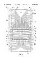
- FIGS. 3 and 4a semiconductor device 70 having a semiconductor die 72/lead frame 76 configuration of the invention is depicted.
- the semiconductor die 72is positioned transversely relative to the lead frame 76, i.e. such that its long sides 86 are perpendicular to the opposing rows 96 of outer lead ends.
- the semiconductor die 72is shown as having peripheral rows 82A, 82B of bond pads 84 along opposing long sides 86, parallel to the longitudinal centerline 90 of the semiconductor die 72.
- the rows 82A, 82B of bond pads 84are shown as generally extending between the opposed short sides 88 of the semiconductor die 72.
- the lead frame 76is shown with three sets 100, 102, 104 of inner leads 78 and outer leads 80.
- a first set 100has non-LOC inner leads 78 which are positioned off-die for wire-bonding with wires 98 to bond pads 84 of row 82A.
- a second set 102has non-LOC inner leads 78 which are also positioned off-die for wire-bonding with conductive wires 98 to bond pads 84 of row 82B.
- a third set 104has LOC inner leads 78 which are adhesively joined to the active surface 94 of the semiconductor die 72 with an intervening insulative layer 92, i.e. as leads over chip (LOC) leads.
- the third set 104is positioned between the two rows 82A, 82B of bond pads 84 and includes leads wire-bonded to both rows.
- the minimum width 106 of the critical function non-LOC inner leads 78 of lead set 100 in semiconductor device 70is about 30-60 percent greater than the minimum inner lead width 56 of the comparable leads in device 10 of drawing FIG. 2.
- the twelve LOC inner leads 78 of lead set 104are shown as having a width 110 nearly double that of width 56 of the bulk of the LOC inner leads 18 of the prior art device of drawing FIG. 2.
- the sixteen non-LOC inner leads 78 of lead set 102are shown to have a width 108 which is about 30 to 100 percent greater than the inner lead width 56 of nearly all LOC leads 18 of the device of drawing FIG. 2.
- the twenty eight non-LOC leads 78 of lead set 100are shown as having a width 106 roughly comparable to the inner lead width 56 of nearly all LOC inner leads of the device of drawing FIG. 2.
- critical leads subject to inductancehave a greater width while non-critical leads are formed with a reduced width.
- the lead widthsmay be adjusted as needed for the particular use of the device.
- the inventionpresents, on average, inner leads having a shorter length of the minimum width portions than the prior art device of drawing FIG. 2. Moreover, the range of lead lengths is much greater. Thus, in the particular example of drawing FIG. 3, twelve leads with very abbreviated lengths are positioned near the semiconductor die corners to carry critical signals subject to inductance.
- the semiconductor device 70is formed by adhesively joining a semiconductor die 72 to a substrate 74 with an intervening insulative layer 112.
- the hybrid lead frame 76includes a set 102 of non-LOC inner leads 78 which are attached by conductive wires 98 to a row 82B of bond pads 84.
- Another set 104 of LOC inner leads 78overlies the active surface 94 of semiconductor die 72 in a LOC configuration and is adhesively joined to the die with an intervening insulative layer 92.
- the LOC lead set 104is thus at a different level than the non-LOC lead sets 102 (and 100, not visible in FIG. 4).
- the outer leads 80terminate in lead ends 114 which may be straight or formed as J-leads or L-leads, etc., as known in the art.
- the lead widths 108 and 110are illustrated in the figure.
- the lead frame 76 and attached semiconductor die 72are encapsulated and extraneous lead frame portions excised to form a device package.
- the semiconductor device 70may be formed without a permanent substrate 74.
- the semiconductor die 72may be separately supported during attachment of the LOC lead frame 76, and the final encapsulated package outline may be represented by the edges 75.
- the non-LOC leads and LOC leadsmay be in the same horizontal plane.
- the inventionprovides wider and generally shorter inner leads 78 for small semiconductor dies 72. This obviates problems with inductance at high speed operation, making the design extremely useful for state-of-the-art applications.
- the LOC leads overlying a large portion of the active surfacealso result in enhanced heat transfer, improving the overall operation of the device.
- the term "long side”includes sides having a length equal to or greater than that of the "short side".
- the semiconductor die 72is shown as rectangular in surface shape, but may be of other shapes provided space is provided between two sets of bond pads for entry of a significant number of LOC leads.
- transverse hybrid LOC semiconductor packageparticularly useful with small dice and in enhancing the construction and operability of a semiconductor package.
- the devicehas been described and illustrated with reference to a specific embodiment thereof, it is not intended that the invention be limited by the illustrated embodiment.
- the inventionis not limited to devices having a specific number or type of leads, bond pads, or dies, nor to a device with a permanent substrate supporting the die.
- this inventionencompass all such modifications and variations which fall within the scope of the appended claims.
Landscapes
- Engineering & Computer Science (AREA)
- Computer Hardware Design (AREA)
- Microelectronics & Electronic Packaging (AREA)
- Power Engineering (AREA)
- Physics & Mathematics (AREA)
- Condensed Matter Physics & Semiconductors (AREA)
- General Physics & Mathematics (AREA)
- Wire Bonding (AREA)
Abstract
Description
Claims (14)
Priority Applications (5)
| Application Number | Priority Date | Filing Date | Title |
|---|---|---|---|
| US09/302,196US6150710A (en) | 1998-08-20 | 1999-04-29 | Transverse hybrid LOC package |
| US09/614,403US6259153B1 (en) | 1998-08-20 | 2000-07-12 | Transverse hybrid LOC package |
| US09/832,539US6406943B2 (en) | 1998-08-20 | 2001-04-11 | Transverse hybrid LOC package |
| US10/118,365US6531342B2 (en) | 1998-08-20 | 2002-04-08 | Method for transverse hybrid loc package |
| US10/369,044US6835604B2 (en) | 1998-08-20 | 2003-02-18 | Methods for transverse hybrid LOC package |
Applications Claiming Priority (2)
| Application Number | Priority Date | Filing Date | Title |
|---|---|---|---|
| US09/137,782US6124150A (en) | 1998-08-20 | 1998-08-20 | Transverse hybrid LOC package |
| US09/302,196US6150710A (en) | 1998-08-20 | 1999-04-29 | Transverse hybrid LOC package |
Related Parent Applications (1)
| Application Number | Title | Priority Date | Filing Date |
|---|---|---|---|
| US09/137,782DivisionUS6124150A (en) | 1998-08-20 | 1998-08-20 | Transverse hybrid LOC package |
Related Child Applications (2)
| Application Number | Title | Priority Date | Filing Date |
|---|---|---|---|
| US09/614,403ContinuationUS6259153B1 (en) | 1998-08-20 | 2000-07-12 | Transverse hybrid LOC package |
| US09614403Continuation | 2001-07-12 |
Publications (1)
| Publication Number | Publication Date |
|---|---|
| US6150710Atrue US6150710A (en) | 2000-11-21 |
Family
ID=22479023
Family Applications (9)
| Application Number | Title | Priority Date | Filing Date |
|---|---|---|---|
| US09/137,782Expired - LifetimeUS6124150A (en) | 1998-08-20 | 1998-08-20 | Transverse hybrid LOC package |
| US09/302,196Expired - LifetimeUS6150710A (en) | 1998-08-20 | 1999-04-29 | Transverse hybrid LOC package |
| US09/539,093Expired - LifetimeUS6218216B1 (en) | 1998-08-20 | 2000-03-30 | Transverse hybrid LOC package |
| US09/614,403Expired - LifetimeUS6259153B1 (en) | 1998-08-20 | 2000-07-12 | Transverse hybrid LOC package |
| US09/824,955Expired - LifetimeUS6476468B2 (en) | 1998-08-20 | 2001-04-03 | Transverse hybrid LOC package |
| US09/832,539Expired - Fee RelatedUS6406943B2 (en) | 1998-08-20 | 2001-04-11 | Transverse hybrid LOC package |
| US10/118,365Expired - LifetimeUS6531342B2 (en) | 1998-08-20 | 2002-04-08 | Method for transverse hybrid loc package |
| US10/222,067Expired - LifetimeUS6753598B2 (en) | 1998-08-20 | 2002-08-16 | Transverse hybrid LOC package |
| US10/369,044Expired - Fee RelatedUS6835604B2 (en) | 1998-08-20 | 2003-02-18 | Methods for transverse hybrid LOC package |
Family Applications Before (1)
| Application Number | Title | Priority Date | Filing Date |
|---|---|---|---|
| US09/137,782Expired - LifetimeUS6124150A (en) | 1998-08-20 | 1998-08-20 | Transverse hybrid LOC package |
Family Applications After (7)
| Application Number | Title | Priority Date | Filing Date |
|---|---|---|---|
| US09/539,093Expired - LifetimeUS6218216B1 (en) | 1998-08-20 | 2000-03-30 | Transverse hybrid LOC package |
| US09/614,403Expired - LifetimeUS6259153B1 (en) | 1998-08-20 | 2000-07-12 | Transverse hybrid LOC package |
| US09/824,955Expired - LifetimeUS6476468B2 (en) | 1998-08-20 | 2001-04-03 | Transverse hybrid LOC package |
| US09/832,539Expired - Fee RelatedUS6406943B2 (en) | 1998-08-20 | 2001-04-11 | Transverse hybrid LOC package |
| US10/118,365Expired - LifetimeUS6531342B2 (en) | 1998-08-20 | 2002-04-08 | Method for transverse hybrid loc package |
| US10/222,067Expired - LifetimeUS6753598B2 (en) | 1998-08-20 | 2002-08-16 | Transverse hybrid LOC package |
| US10/369,044Expired - Fee RelatedUS6835604B2 (en) | 1998-08-20 | 2003-02-18 | Methods for transverse hybrid LOC package |
Country Status (1)
| Country | Link |
|---|---|
| US (9) | US6124150A (en) |
Cited By (28)
| Publication number | Priority date | Publication date | Assignee | Title |
|---|---|---|---|---|
| US20020140077A1 (en)* | 1998-02-27 | 2002-10-03 | Micron Technology, Inc. | Multichip semiconductor package |
| US6476468B2 (en)* | 1998-08-20 | 2002-11-05 | Micron Technology, Inc. | Transverse hybrid LOC package |
| US6564979B2 (en) | 2001-07-18 | 2003-05-20 | Micron Technology, Inc. | Method and apparatus for dispensing adhesive on microelectronic substrate supports |
| US20030104654A1 (en)* | 2000-06-28 | 2003-06-05 | Farnworth Warren M. | Recessed encapsulated microelectronic devices and methods for formation |
| US20040026773A1 (en)* | 2002-08-08 | 2004-02-12 | Koon Eng Meow | Packaged microelectronic components |
| US20040026776A1 (en)* | 2002-08-08 | 2004-02-12 | Brand Joseph M. | Microelectronic devices and methods for manufacturing and operating packaged microelectronic device assemblies |
| US20040159921A1 (en)* | 2001-12-26 | 2004-08-19 | Stephen Moxham | Methods for coupling a flowable conductive material to microelectronic substrates |
| US20040173899A1 (en)* | 2003-03-04 | 2004-09-09 | Peng Neo Chee | Microelectronic component assemblies employing lead frames having reduced-thickness inner lengths |
| US20040177984A1 (en)* | 2003-03-11 | 2004-09-16 | Groothuis Steven K. | Microelectronic component assemblies having lead frames adapted to reduce package bow |
| US20040238909A1 (en)* | 2003-05-30 | 2004-12-02 | Boon Suan Jeung | Packaged microelectronic devices and methods of packaging microelectronic devices |
| US20050045378A1 (en)* | 2003-08-29 | 2005-03-03 | Heng Mung Suan | Stacked microfeature devices and associated methods |
| US6876066B2 (en) | 2001-08-29 | 2005-04-05 | Micron Technology, Inc. | Packaged microelectronic devices and methods of forming same |
| US20050156294A1 (en)* | 2003-01-06 | 2005-07-21 | Micron Technology, Inc. | Microelectronic component assemblies and microelectronic component lead frame structures |
| US6951982B2 (en) | 2002-11-22 | 2005-10-04 | Micron Technology, Inc. | Packaged microelectronic component assemblies |
| US20050250251A1 (en)* | 2000-08-23 | 2005-11-10 | Corisis David J | Method and apparatus for decoupling conductive portions of a microelectronic device package |
| US20060040428A1 (en)* | 2004-08-19 | 2006-02-23 | Johnson Mark S | Conductive structures for microfeature devices and methods for fabricating microfeature devices |
| US20060043611A1 (en)* | 2004-09-01 | 2006-03-02 | Kinsman Larry D | Reduced-dimension microelectronic component assemblies with wire bonds and methods of making same |
| US7259451B2 (en) | 2003-08-29 | 2007-08-21 | Micron Technology, Inc. | Invertible microfeature device packages |
| US20070210441A1 (en)* | 2006-03-08 | 2007-09-13 | Micron Technology, Inc. | Microelectronic device assemblies including assemblies with recurved leadframes, and associated methods |
| US20080006940A1 (en)* | 2006-07-05 | 2008-01-10 | Micron Technology, Inc. | Lead frames, microelectronic devices with lead frames, and methods for manufacturing lead frames and microelectronic devices with lead frames |
| US20080012110A1 (en)* | 2006-07-17 | 2008-01-17 | Micron Technology, Inc. | Microelectronic packages with leadframes, including leadframes configured for stacked die packages, and associated systems and methods |
| US7365424B2 (en) | 2004-07-23 | 2008-04-29 | Micron Technology, Inc. | Microelectronic component assemblies with recessed wire bonds and methods of making same |
| US20090026592A1 (en)* | 2007-07-24 | 2009-01-29 | Micron Technology, Inc. | Semiconductor dies with recesses, associated leadframes, and associated systems and methods |
| US20090026593A1 (en)* | 2007-07-24 | 2009-01-29 | Micron Technology, Inc. | Thin semiconductor die packages and associated systems and methods |
| US7622377B2 (en) | 2005-09-01 | 2009-11-24 | Micron Technology, Inc. | Microfeature workpiece substrates having through-substrate vias, and associated methods of formation |
| US7671459B2 (en) | 2006-02-08 | 2010-03-02 | Micron Technologies, Inc. | Microelectronic devices, stacked microelectronic devices, and methods for manufacturing such devices |
| US7843050B2 (en) | 2007-07-24 | 2010-11-30 | Micron Technology, Inc. | Microelectronic die packages with metal leads, including metal leads for stacked die packages, and associated systems and methods |
| US7947529B2 (en) | 2007-08-16 | 2011-05-24 | Micron Technology, Inc. | Microelectronic die packages with leadframes, including leadframe-based interposer for stacked die packages, and associated systems and methods |
Families Citing this family (55)
| Publication number | Priority date | Publication date | Assignee | Title |
|---|---|---|---|---|
| US6114756A (en)* | 1998-04-01 | 2000-09-05 | Micron Technology, Inc. | Interdigitated capacitor design for integrated circuit leadframes |
| US6551337B1 (en) | 1999-10-05 | 2003-04-22 | Omnisonics Medical Technologies, Inc. | Ultrasonic medical device operating in a transverse mode |
| US6524251B2 (en) | 1999-10-05 | 2003-02-25 | Omnisonics Medical Technologies, Inc. | Ultrasonic device for tissue ablation and sheath for use therewith |
| US20040097996A1 (en) | 1999-10-05 | 2004-05-20 | Omnisonics Medical Technologies, Inc. | Apparatus and method of removing occlusions using an ultrasonic medical device operating in a transverse mode |
| US6558600B1 (en) | 2000-05-04 | 2003-05-06 | Micron Technology, Inc. | Method for packaging microelectronic substrates |
| AU2001259681A1 (en) | 2000-05-08 | 2001-11-20 | Micron Technology, Inc. | Method and apparatus for distributing mold material in a mold for packaging microelectronic devices |
| US6303469B1 (en) | 2000-06-07 | 2001-10-16 | Micron Technology, Inc. | Thin microelectronic substrates and methods of manufacture |
| US6589820B1 (en) | 2000-06-16 | 2003-07-08 | Micron Technology, Inc. | Method and apparatus for packaging a microelectronic die |
| US6365434B1 (en) | 2000-06-28 | 2002-04-02 | Micron Technology, Inc. | Method and apparatus for reduced flash encapsulation of microelectronic devices |
| US7273769B1 (en)* | 2000-08-16 | 2007-09-25 | Micron Technology, Inc. | Method and apparatus for removing encapsulating material from a packaged microelectronic device |
| US6483044B1 (en)* | 2000-08-23 | 2002-11-19 | Micron Technology, Inc. | Interconnecting substrates for electrical coupling of microelectronic components |
| US6979595B1 (en) | 2000-08-24 | 2005-12-27 | Micron Technology, Inc. | Packaged microelectronic devices with pressure release elements and methods for manufacturing and using such packaged microelectronic devices |
| US6541849B1 (en)* | 2000-08-25 | 2003-04-01 | Micron Technology, Inc. | Memory device power distribution |
| US6838760B1 (en)* | 2000-08-28 | 2005-01-04 | Micron Technology, Inc. | Packaged microelectronic devices with interconnecting units |
| JP2002076233A (en)* | 2000-09-04 | 2002-03-15 | Mitsubishi Electric Corp | Semiconductor device |
| WO2002070158A1 (en)* | 2001-03-07 | 2002-09-12 | Omnisonics Medical Technologies, Inc. | Apparatus and method for manufacturing small diameter medical devices |
| US7169785B2 (en)* | 2001-09-21 | 2007-01-30 | Reddy Us Therapeutics, Inc. | Methods and compositions of novel triazine compounds |
| US6622380B1 (en) | 2002-02-12 | 2003-09-23 | Micron Technology, Inc. | Methods for manufacturing microelectronic devices and methods for mounting microelectronic packages to circuit boards |
| US7109588B2 (en)* | 2002-04-04 | 2006-09-19 | Micron Technology, Inc. | Method and apparatus for attaching microelectronic substrates and support members |
| US6621150B1 (en)* | 2002-07-10 | 2003-09-16 | Siliconware Precision Industries Co., Ltd. | Lead frame adaptable to the trend of IC packaging |
| JP2004063565A (en)* | 2002-07-25 | 2004-02-26 | Seiko Epson Corp | Semiconductor device and its manufacturing method, circuit board, and electronic equipment |
| US7326594B2 (en)* | 2002-07-31 | 2008-02-05 | Microchip Technology Incorporated | Connecting a plurality of bond pads and/or inner leads with a single bond wire |
| US7157790B2 (en)* | 2002-07-31 | 2007-01-02 | Microchip Technology Inc. | Single die stitch bonding |
| SG127684A1 (en)* | 2002-08-19 | 2006-12-29 | Micron Technology Inc | Packaged microelectronic component assemblies |
| US6740546B2 (en)* | 2002-08-21 | 2004-05-25 | Micron Technology, Inc. | Packaged microelectronic devices and methods for assembling microelectronic devices |
| US6784525B2 (en)* | 2002-10-29 | 2004-08-31 | Micron Technology, Inc. | Semiconductor component having multi layered leadframe |
| US6812084B2 (en)* | 2002-12-09 | 2004-11-02 | Progressant Technologies, Inc. | Adaptive negative differential resistance device |
| US6879050B2 (en)* | 2003-02-11 | 2005-04-12 | Micron Technology, Inc. | Packaged microelectronic devices and methods for packaging microelectronic devices |
| KR100475740B1 (en)* | 2003-02-25 | 2005-03-10 | 삼성전자주식회사 | semiconductor intergrated circuit having pads layout for improving signal integrity and for reducing chip size |
| ATE388488T1 (en)* | 2003-03-07 | 2008-03-15 | Nxp Bv | SEMICONDUCTOR COMPONENT, SEMICONDUCTOR BODY AND METHOD FOR THE PRODUCTION THEREOF |
| US6921860B2 (en) | 2003-03-18 | 2005-07-26 | Micron Technology, Inc. | Microelectronic component assemblies having exposed contacts |
| US7227095B2 (en)* | 2003-08-06 | 2007-06-05 | Micron Technology, Inc. | Wire bonders and methods of wire-bonding |
| SG153627A1 (en)* | 2003-10-31 | 2009-07-29 | Micron Technology Inc | Reduced footprint packaged microelectronic components and methods for manufacturing such microelectronic components |
| US7091124B2 (en) | 2003-11-13 | 2006-08-15 | Micron Technology, Inc. | Methods for forming vias in microelectronic devices, and methods for packaging microelectronic devices |
| US8084866B2 (en)* | 2003-12-10 | 2011-12-27 | Micron Technology, Inc. | Microelectronic devices and methods for filling vias in microelectronic devices |
| US7794414B2 (en) | 2004-02-09 | 2010-09-14 | Emigrant Bank, N.A. | Apparatus and method for an ultrasonic medical device operating in torsional and transverse modes |
| US6929485B1 (en)* | 2004-03-16 | 2005-08-16 | Agilent Technologies, Inc. | Lead frame with interdigitated pins |
| US7157310B2 (en)* | 2004-09-01 | 2007-01-02 | Micron Technology, Inc. | Methods for packaging microfeature devices and microfeature devices formed by such methods |
| US8278751B2 (en) | 2005-02-08 | 2012-10-02 | Micron Technology, Inc. | Methods of adhering microfeature workpieces, including a chip, to a support member |
| SG130061A1 (en)* | 2005-08-24 | 2007-03-20 | Micron Technology Inc | Microelectronic devices and microelectronic support devices, and associated assemblies and methods |
| US7807505B2 (en)* | 2005-08-30 | 2010-10-05 | Micron Technology, Inc. | Methods for wafer-level packaging of microfeature devices and microfeature devices formed using such methods |
| US7745944B2 (en) | 2005-08-31 | 2010-06-29 | Micron Technology, Inc. | Microelectronic devices having intermediate contacts for connection to interposer substrates, and associated methods of packaging microelectronic devices with intermediate contacts |
| US7633157B2 (en)* | 2005-12-13 | 2009-12-15 | Micron Technology, Inc. | Microelectronic devices having a curved surface and methods for manufacturing the same |
| US20070148820A1 (en)* | 2005-12-22 | 2007-06-28 | Micron Technology, Inc. | Microelectronic devices and methods for manufacturing microelectronic devices |
| SG133445A1 (en)* | 2005-12-29 | 2007-07-30 | Micron Technology Inc | Methods for packaging microelectronic devices and microelectronic devices formed using such methods |
| SG136009A1 (en) | 2006-03-29 | 2007-10-29 | Micron Technology Inc | Packaged microelectronic devices recessed in support member cavities, and associated methods |
| US7910385B2 (en)* | 2006-05-12 | 2011-03-22 | Micron Technology, Inc. | Method of fabricating microelectronic devices |
| US8749782B1 (en) | 2006-12-19 | 2014-06-10 | J.A. Woollam Co., Inc. | DLP base small spot investigation system |
| US7777878B2 (en)* | 2006-12-19 | 2010-08-17 | J.A. Woollam Co., Inc. | Application of digital light processor in scanning spectrometer and imaging ellipsometer and the like systems |
| US8345241B1 (en) | 2006-12-19 | 2013-01-01 | J. A. Woollam Co., Inc. | Application of digital light processor in imaging ellipsometer and the like systems |
| US7833456B2 (en) | 2007-02-23 | 2010-11-16 | Micron Technology, Inc. | Systems and methods for compressing an encapsulant adjacent a semiconductor workpiece |
| US7750449B2 (en)* | 2007-03-13 | 2010-07-06 | Micron Technology, Inc. | Packaged semiconductor components having substantially rigid support members and methods of packaging semiconductor components |
| US7955898B2 (en) | 2007-03-13 | 2011-06-07 | Micron Technology, Inc. | Packaged microelectronic devices and methods for manufacturing packaged microelectronic devices |
| CA2805814C (en) | 2010-08-06 | 2016-04-26 | Dna Electronics Ltd. | Method and apparatus for sensing a property of a fluid |
| CN103928431B (en)* | 2012-10-31 | 2017-03-01 | 矽力杰半导体技术(杭州)有限公司 | A kind of flip-chip packaged device |
Citations (38)
| Publication number | Priority date | Publication date | Assignee | Title |
|---|---|---|---|---|
| US4033844A (en)* | 1975-11-03 | 1977-07-05 | National Semiconductor Corporation | Apparatus for selectively plating lead frames |
| US4089733A (en)* | 1975-09-12 | 1978-05-16 | Amp Incorporated | Method of forming complex shaped metal-plastic composite lead frames for IC packaging |
| US4279682A (en)* | 1978-11-02 | 1981-07-21 | Sumitomo Metal Mining Company Limited | Apparatus for securing tape to leads of semiconductor lead frame |
| JPS60105658A (en)* | 1973-02-19 | 1985-06-11 | ロレアル | Manufacture of bornylidene |
| US4801999A (en)* | 1987-07-15 | 1989-01-31 | Advanced Micro Devices, Inc. | Integrated circuit lead frame assembly containing voltage bussing and distribution to an integrated circuit die using tape automated bonding with two metal layers |
| US4835120A (en)* | 1987-01-12 | 1989-05-30 | Debendra Mallik | Method of making a multilayer molded plastic IC package |
| US4862245A (en)* | 1985-04-18 | 1989-08-29 | International Business Machines Corporation | Package semiconductor chip |
| US4891687A (en)* | 1987-01-12 | 1990-01-02 | Intel Corporation | Multi-layer molded plastic IC package |
| US4894752A (en)* | 1987-07-14 | 1990-01-16 | Shinko Electric Industries, Co., Ltd. | Lead frame for a semiconductor device |
| JPH02156547A (en)* | 1988-12-08 | 1990-06-15 | Matsushita Electric Ind Co Ltd | Flexible board and method of testing integrated circuit |
| US4937656A (en)* | 1988-04-22 | 1990-06-26 | Mitsubishi Denki Kabushiki Kaisha | Semiconductor device |
| US4943843A (en)* | 1985-03-25 | 1990-07-24 | Hitachi, Ltd. | Semiconductor device |
| US4984059A (en)* | 1982-10-08 | 1991-01-08 | Fujitsu Limited | Semiconductor device and a method for fabricating the same |
| US4989068A (en)* | 1988-02-12 | 1991-01-29 | Hitachi, Ltd. | Semiconductor device and method of manufacturing the same |
| JPH0335589A (en)* | 1989-06-30 | 1991-02-15 | Ibiden Co Ltd | Formation of overlay plating on electronic component mounting board |
| US5140404A (en)* | 1990-10-24 | 1992-08-18 | Micron Technology, Inc. | Semiconductor device manufactured by a method for attaching a semiconductor die to a leadframe using a thermoplastic covered carrier tape |
| US5142450A (en)* | 1991-04-12 | 1992-08-25 | Motorola, Inc. | Non-contact lead design and package |
| US5184208A (en)* | 1987-06-30 | 1993-02-02 | Hitachi, Ltd. | Semiconductor device |
| US5218229A (en)* | 1991-08-30 | 1993-06-08 | Micron Technology, Inc. | Inset die lead frame configuration lead frame for a semiconductor device having means for improved busing and die-lead frame attachment |
| US5227661A (en)* | 1990-09-24 | 1993-07-13 | Texas Instruments Incorporated | Integrated circuit device having an aminopropyltriethoxysilane coating |
| US5227662A (en)* | 1990-05-24 | 1993-07-13 | Nippon Steel Corporation | Composite lead frame and semiconductor device using the same |
| US5229639A (en)* | 1991-10-31 | 1993-07-20 | International Business Machines Corporation | Low powder distribution inductance lead frame for semiconductor chips |
| US5231755A (en)* | 1991-08-20 | 1993-08-03 | Emanuel Technology, Inc. | Method of forming soluble alignment bars |
| US5233220A (en)* | 1989-06-30 | 1993-08-03 | Texas Instruments Incorporated | Balanced capacitance lead frame for integrated circuits and integrated circuit device with separate conductive layer |
| US5252853A (en)* | 1991-09-19 | 1993-10-12 | Mitsubishi Denki Kabushiki Kaisha | Packaged semiconductor device having tab tape and particular power distribution lead structure |
| EP0576021A1 (en)* | 1992-06-24 | 1993-12-29 | Kabushiki Kaisha Toshiba | Lead on chip structure for semiconductor device |
| US5286679A (en)* | 1993-03-18 | 1994-02-15 | Micron Technology, Inc. | Method for attaching a semiconductor die to a leadframe using a patterned adhesive layer |
| US5304842A (en)* | 1990-10-24 | 1994-04-19 | Micron Technology, Inc. | Dissimilar adhesive die attach for semiconductor devices |
| US5331200A (en)* | 1992-09-30 | 1994-07-19 | Texas Instruments Incorporated | Lead-on-chip inner lead bonding lead frame method and apparatus |
| US5331201A (en)* | 1991-12-24 | 1994-07-19 | Sony Corporation | Semiconductor device having inner lead arrangement with enhanced stability |
| US5352633A (en)* | 1992-06-02 | 1994-10-04 | Texas Instruments Incorporated | Semiconductor lead frame lead stabilization |
| US5461255A (en)* | 1992-09-18 | 1995-10-24 | Texas Instruments Incorporated | Multi-layered lead frame assembly for integrated circuits |
| US5466888A (en)* | 1991-03-20 | 1995-11-14 | Hitachi, Ltd. | Packaged semiconductor device having stress absorbing film |
| US5471369A (en)* | 1993-07-09 | 1995-11-28 | Fujitsu Limited | Semiconductor device having a plurality of semiconductor chips |
| US5475918A (en)* | 1993-10-01 | 1995-12-19 | Electroplating Engineers Of Japan Ltd. | Method of preventing deformation of lead frames |
| US5521426A (en)* | 1992-09-09 | 1996-05-28 | Texas Instruments Incorporated | Reduced capacitance lead frame for lead on chip package |
| US5592019A (en)* | 1994-04-19 | 1997-01-07 | Mitsubishi Denki Kabushiki Kaisha | Semiconductor device and module |
| US5883427A (en)* | 1996-09-10 | 1999-03-16 | Mitsubishi Denki Kabushiki Kaisha | Semiconductor device power supply wiring structure |
Family Cites Families (5)
| Publication number | Priority date | Publication date | Assignee | Title |
|---|---|---|---|---|
| US5234866A (en)* | 1985-03-25 | 1993-08-10 | Hitachi, Ltd. | Semiconductor device and process for producing the same, and lead frame used in said process |
| JPH08148603A (en)* | 1994-11-22 | 1996-06-07 | Nec Kyushu Ltd | Ball grid array type semiconductor device and manufacture thereof |
| US5907769A (en)* | 1996-12-30 | 1999-05-25 | Micron Technology, Inc. | Leads under chip in conventional IC package |
| JPH10242368A (en)* | 1997-02-25 | 1998-09-11 | Hitachi Ltd | Semiconductor device and manufacturing method thereof, semiconductor module and IC card |
| US6124150A (en)* | 1998-08-20 | 2000-09-26 | Micron Technology, Inc. | Transverse hybrid LOC package |
- 1998
- 1998-08-20USUS09/137,782patent/US6124150A/ennot_activeExpired - Lifetime
- 1999
- 1999-04-29USUS09/302,196patent/US6150710A/ennot_activeExpired - Lifetime
- 2000
- 2000-03-30USUS09/539,093patent/US6218216B1/ennot_activeExpired - Lifetime
- 2000-07-12USUS09/614,403patent/US6259153B1/ennot_activeExpired - Lifetime
- 2001
- 2001-04-03USUS09/824,955patent/US6476468B2/ennot_activeExpired - Lifetime
- 2001-04-11USUS09/832,539patent/US6406943B2/ennot_activeExpired - Fee Related
- 2002
- 2002-04-08USUS10/118,365patent/US6531342B2/ennot_activeExpired - Lifetime
- 2002-08-16USUS10/222,067patent/US6753598B2/ennot_activeExpired - Lifetime
- 2003
- 2003-02-18USUS10/369,044patent/US6835604B2/ennot_activeExpired - Fee Related
Patent Citations (39)
| Publication number | Priority date | Publication date | Assignee | Title |
|---|---|---|---|---|
| JPS60105658A (en)* | 1973-02-19 | 1985-06-11 | ロレアル | Manufacture of bornylidene |
| US4089733A (en)* | 1975-09-12 | 1978-05-16 | Amp Incorporated | Method of forming complex shaped metal-plastic composite lead frames for IC packaging |
| US4033844A (en)* | 1975-11-03 | 1977-07-05 | National Semiconductor Corporation | Apparatus for selectively plating lead frames |
| US4279682A (en)* | 1978-11-02 | 1981-07-21 | Sumitomo Metal Mining Company Limited | Apparatus for securing tape to leads of semiconductor lead frame |
| US4984059A (en)* | 1982-10-08 | 1991-01-08 | Fujitsu Limited | Semiconductor device and a method for fabricating the same |
| US4943843A (en)* | 1985-03-25 | 1990-07-24 | Hitachi, Ltd. | Semiconductor device |
| US4862245A (en)* | 1985-04-18 | 1989-08-29 | International Business Machines Corporation | Package semiconductor chip |
| US4891687A (en)* | 1987-01-12 | 1990-01-02 | Intel Corporation | Multi-layer molded plastic IC package |
| US4835120A (en)* | 1987-01-12 | 1989-05-30 | Debendra Mallik | Method of making a multilayer molded plastic IC package |
| US5184208A (en)* | 1987-06-30 | 1993-02-02 | Hitachi, Ltd. | Semiconductor device |
| US4894752A (en)* | 1987-07-14 | 1990-01-16 | Shinko Electric Industries, Co., Ltd. | Lead frame for a semiconductor device |
| US4801999A (en)* | 1987-07-15 | 1989-01-31 | Advanced Micro Devices, Inc. | Integrated circuit lead frame assembly containing voltage bussing and distribution to an integrated circuit die using tape automated bonding with two metal layers |
| US4989068A (en)* | 1988-02-12 | 1991-01-29 | Hitachi, Ltd. | Semiconductor device and method of manufacturing the same |
| US4937656A (en)* | 1988-04-22 | 1990-06-26 | Mitsubishi Denki Kabushiki Kaisha | Semiconductor device |
| JPH02156547A (en)* | 1988-12-08 | 1990-06-15 | Matsushita Electric Ind Co Ltd | Flexible board and method of testing integrated circuit |
| JPH0335589A (en)* | 1989-06-30 | 1991-02-15 | Ibiden Co Ltd | Formation of overlay plating on electronic component mounting board |
| US5233220A (en)* | 1989-06-30 | 1993-08-03 | Texas Instruments Incorporated | Balanced capacitance lead frame for integrated circuits and integrated circuit device with separate conductive layer |
| US5227662A (en)* | 1990-05-24 | 1993-07-13 | Nippon Steel Corporation | Composite lead frame and semiconductor device using the same |
| US5418189A (en)* | 1990-09-24 | 1995-05-23 | Texas Instruments Incorporated | Integrated circuit device and method to prevent cracking during surface mount |
| US5227661A (en)* | 1990-09-24 | 1993-07-13 | Texas Instruments Incorporated | Integrated circuit device having an aminopropyltriethoxysilane coating |
| US5304842A (en)* | 1990-10-24 | 1994-04-19 | Micron Technology, Inc. | Dissimilar adhesive die attach for semiconductor devices |
| US5140404A (en)* | 1990-10-24 | 1992-08-18 | Micron Technology, Inc. | Semiconductor device manufactured by a method for attaching a semiconductor die to a leadframe using a thermoplastic covered carrier tape |
| US5466888A (en)* | 1991-03-20 | 1995-11-14 | Hitachi, Ltd. | Packaged semiconductor device having stress absorbing film |
| US5142450A (en)* | 1991-04-12 | 1992-08-25 | Motorola, Inc. | Non-contact lead design and package |
| US5231755A (en)* | 1991-08-20 | 1993-08-03 | Emanuel Technology, Inc. | Method of forming soluble alignment bars |
| US5218229A (en)* | 1991-08-30 | 1993-06-08 | Micron Technology, Inc. | Inset die lead frame configuration lead frame for a semiconductor device having means for improved busing and die-lead frame attachment |
| US5252853A (en)* | 1991-09-19 | 1993-10-12 | Mitsubishi Denki Kabushiki Kaisha | Packaged semiconductor device having tab tape and particular power distribution lead structure |
| US5229639A (en)* | 1991-10-31 | 1993-07-20 | International Business Machines Corporation | Low powder distribution inductance lead frame for semiconductor chips |
| US5331201A (en)* | 1991-12-24 | 1994-07-19 | Sony Corporation | Semiconductor device having inner lead arrangement with enhanced stability |
| US5352633A (en)* | 1992-06-02 | 1994-10-04 | Texas Instruments Incorporated | Semiconductor lead frame lead stabilization |
| EP0576021A1 (en)* | 1992-06-24 | 1993-12-29 | Kabushiki Kaisha Toshiba | Lead on chip structure for semiconductor device |
| US5521426A (en)* | 1992-09-09 | 1996-05-28 | Texas Instruments Incorporated | Reduced capacitance lead frame for lead on chip package |
| US5461255A (en)* | 1992-09-18 | 1995-10-24 | Texas Instruments Incorporated | Multi-layered lead frame assembly for integrated circuits |
| US5331200A (en)* | 1992-09-30 | 1994-07-19 | Texas Instruments Incorporated | Lead-on-chip inner lead bonding lead frame method and apparatus |
| US5286679A (en)* | 1993-03-18 | 1994-02-15 | Micron Technology, Inc. | Method for attaching a semiconductor die to a leadframe using a patterned adhesive layer |
| US5471369A (en)* | 1993-07-09 | 1995-11-28 | Fujitsu Limited | Semiconductor device having a plurality of semiconductor chips |
| US5475918A (en)* | 1993-10-01 | 1995-12-19 | Electroplating Engineers Of Japan Ltd. | Method of preventing deformation of lead frames |
| US5592019A (en)* | 1994-04-19 | 1997-01-07 | Mitsubishi Denki Kabushiki Kaisha | Semiconductor device and module |
| US5883427A (en)* | 1996-09-10 | 1999-03-16 | Mitsubishi Denki Kabushiki Kaisha | Semiconductor device power supply wiring structure |
Non-Patent Citations (4)
| Title |
|---|
| Caroline A. Kovac, "Plastic Package Fabricaton", pps. 470-482. |
| Caroline A. Kovac, Plastic Package Fabricaton , pps. 470 482.* |
| Louis T. Manzione, "Plastic Packaging of Microelectronic Devices", pps. 156-347, 1990. |
| Louis T. Manzione, Plastic Packaging of Microelectronic Devices , pps. 156 347, 1990.* |
Cited By (104)
| Publication number | Priority date | Publication date | Assignee | Title |
|---|---|---|---|---|
| US20050212143A1 (en)* | 1998-02-27 | 2005-09-29 | Micron Technology, Inc. | Multichip semiconductor package |
| US6906409B2 (en) | 1998-02-27 | 2005-06-14 | Micron Technology, Inc. | Multichip semiconductor package |
| US20020140077A1 (en)* | 1998-02-27 | 2002-10-03 | Micron Technology, Inc. | Multichip semiconductor package |
| US6476468B2 (en)* | 1998-08-20 | 2002-11-05 | Micron Technology, Inc. | Transverse hybrid LOC package |
| US20020195694A1 (en)* | 1998-08-20 | 2002-12-26 | Corisis David J. | Transverse hybrid LOC package |
| US6531342B2 (en) | 1998-08-20 | 2003-03-11 | Micron Technology, Inst. | Method for transverse hybrid loc package |
| US20030162327A1 (en)* | 1998-08-20 | 2003-08-28 | Corisis David J. | Methods for transverse hybrid LOC package |
| US6835604B2 (en) | 1998-08-20 | 2004-12-28 | Micron Technology, Inc. | Methods for transverse hybrid LOC package |
| US6753598B2 (en)* | 1998-08-20 | 2004-06-22 | Micron Technology, Inc. | Transverse hybrid LOC package |
| US20030104654A1 (en)* | 2000-06-28 | 2003-06-05 | Farnworth Warren M. | Recessed encapsulated microelectronic devices and methods for formation |
| US6841423B2 (en) | 2000-06-28 | 2005-01-11 | Micron Technology, Inc. | Methods for formation of recessed encapsulated microelectronic devices |
| US6819003B2 (en) | 2000-06-28 | 2004-11-16 | Micron Technology Inc. | Recessed encapsulated microelectronic devices and methods for formation |
| US20050250251A1 (en)* | 2000-08-23 | 2005-11-10 | Corisis David J | Method and apparatus for decoupling conductive portions of a microelectronic device package |
| US7378723B2 (en) | 2000-08-23 | 2008-05-27 | Micron Technology, Inc. | Method and apparatus for decoupling conductive portions of a microelectronic device package |
| US7183138B2 (en) | 2000-08-23 | 2007-02-27 | Micron Technology, Inc. | Method and apparatus for decoupling conductive portions of a microelectronic device package |
| US20070052087A1 (en)* | 2000-08-23 | 2007-03-08 | Micron Technology, Inc. | Method and apparatus for decoupling conductive portions of a microelectronic device package |
| US6564979B2 (en) | 2001-07-18 | 2003-05-20 | Micron Technology, Inc. | Method and apparatus for dispensing adhesive on microelectronic substrate supports |
| US6876066B2 (en) | 2001-08-29 | 2005-04-05 | Micron Technology, Inc. | Packaged microelectronic devices and methods of forming same |
| US6943450B2 (en) | 2001-08-29 | 2005-09-13 | Micron Technology, Inc. | Packaged microelectronic devices and methods of forming same |
| US20040159946A1 (en)* | 2001-12-26 | 2004-08-19 | Stephen Moxham | Microelectronic assemblies, electronic devices, and apparatuses for supporting microelectronic substrates |
| US6936916B2 (en) | 2001-12-26 | 2005-08-30 | Micron Technology, Inc. | Microelectronic assemblies and electronic devices including connection structures with multiple elongated members |
| US6870276B1 (en) | 2001-12-26 | 2005-03-22 | Micron Technology, Inc. | Apparatus for supporting microelectronic substrates |
| US6995026B2 (en) | 2001-12-26 | 2006-02-07 | Micron Technology, Inc. | Methods for coupling a flowable conductive material to microelectronic substrates |
| US20040159921A1 (en)* | 2001-12-26 | 2004-08-19 | Stephen Moxham | Methods for coupling a flowable conductive material to microelectronic substrates |
| US20050242437A1 (en)* | 2001-12-26 | 2005-11-03 | Micron Technology, Inc. | Method and apparatus for supporting microelectronic substrates |
| US20040026773A1 (en)* | 2002-08-08 | 2004-02-12 | Koon Eng Meow | Packaged microelectronic components |
| US7306974B2 (en) | 2002-08-08 | 2007-12-11 | Micron Technology, Inc. | Microelectronic devices and methods for manufacturing and operating packaged microelectronic device assemblies |
| US8637973B2 (en) | 2002-08-08 | 2014-01-28 | Micron Technology, Inc. | Packaged microelectronic components with terminals exposed through encapsulant |
| US20040026776A1 (en)* | 2002-08-08 | 2004-02-12 | Brand Joseph M. | Microelectronic devices and methods for manufacturing and operating packaged microelectronic device assemblies |
| US7067905B2 (en) | 2002-08-08 | 2006-06-27 | Micron Technology, Inc. | Packaged microelectronic devices including first and second casings |
| US9418872B2 (en) | 2002-08-08 | 2016-08-16 | Micron Technology, Inc. | Packaged microelectronic components |
| US7195957B2 (en) | 2002-08-08 | 2007-03-27 | Micron Technology, Inc. | Packaged microelectronic components |
| US20060040422A1 (en)* | 2002-08-08 | 2006-02-23 | Micron Technology, Inc. | Microelectronic devices and methods for manufacturing and operating packaged microelectronic device |
| US6951982B2 (en) | 2002-11-22 | 2005-10-04 | Micron Technology, Inc. | Packaged microelectronic component assemblies |
| US7652365B2 (en) | 2003-01-06 | 2010-01-26 | Micron Technologies, Inc. | Microelectronic component assemblies and microelectronic component lead frame structures |
| US7247520B2 (en) | 2003-01-06 | 2007-07-24 | Micron Technology, Inc. | Microelectronic component assemblies and microelectronic component lead frame structures |
| US20080067644A1 (en)* | 2003-01-06 | 2008-03-20 | Micron Technology, Inc. | Microelectronic component assemblies and microelectronic component lead frame structures |
| US7132734B2 (en) | 2003-01-06 | 2006-11-07 | Micron Technology, Inc. | Microelectronic component assemblies and microelectronic component lead frame structures |
| US7923824B2 (en) | 2003-01-06 | 2011-04-12 | Micron Technology, Inc. | Microelectronic component assemblies and microelectronic component lead frame structures |
| US20050156300A1 (en)* | 2003-01-06 | 2005-07-21 | Micron Technology, Inc. | Microelectronic component assemblies and microelectronic component lead frame structures |
| US20050156294A1 (en)* | 2003-01-06 | 2005-07-21 | Micron Technology, Inc. | Microelectronic component assemblies and microelectronic component lead frame structures |
| US7298025B2 (en) | 2003-01-06 | 2007-11-20 | Micron Technology, Inc. | Microelectronic component assemblies and microelectronic component lead frame structures |
| US7057281B2 (en) | 2003-03-04 | 2006-06-06 | Micron Technology Inc. | Microelectronic component assemblies employing lead frames having reduced-thickness inner lengths |
| US7425470B2 (en) | 2003-03-04 | 2008-09-16 | Micron Technology, Inc. | Microelectronic component assemblies employing lead frames having reduced-thickness inner lengths |
| US20040173899A1 (en)* | 2003-03-04 | 2004-09-09 | Peng Neo Chee | Microelectronic component assemblies employing lead frames having reduced-thickness inner lengths |
| US7691680B2 (en) | 2003-03-04 | 2010-04-06 | Micron Technologies, Inc. | Method of fabricating microelectronic component assemblies employing lead frames having reduced-thickness inner lengths |
| US7183485B2 (en) | 2003-03-11 | 2007-02-27 | Micron Technology, Inc. | Microelectronic component assemblies having lead frames adapted to reduce package bow |
| US20040177984A1 (en)* | 2003-03-11 | 2004-09-16 | Groothuis Steven K. | Microelectronic component assemblies having lead frames adapted to reduce package bow |
| US20070128770A1 (en)* | 2003-03-11 | 2007-06-07 | Micron Technology, Inc. | Microelectronic component assemblies having lead frames adapted to reduce package bow |
| US6882021B2 (en) | 2003-05-30 | 2005-04-19 | Micron Technology, Inc. | Packaged image sensing microelectronic devices including a lead and methods of packaging image sensing microelectronic devices including a lead |
| US20040238909A1 (en)* | 2003-05-30 | 2004-12-02 | Boon Suan Jeung | Packaged microelectronic devices and methods of packaging microelectronic devices |
| US20100258939A1 (en)* | 2003-08-29 | 2010-10-14 | Micron Technology, Inc. | Stacked microfeature devices and associated methods |
| US20050045378A1 (en)* | 2003-08-29 | 2005-03-03 | Heng Mung Suan | Stacked microfeature devices and associated methods |
| US8400780B2 (en) | 2003-08-29 | 2013-03-19 | Micron Technology, Inc. | Stacked microfeature devices |
| US11887970B2 (en) | 2003-08-29 | 2024-01-30 | Micron Technology, Inc. | Stacked microfeature devices and associated methods |
| US7368810B2 (en) | 2003-08-29 | 2008-05-06 | Micron Technology, Inc. | Invertible microfeature device packages |
| US7071421B2 (en) | 2003-08-29 | 2006-07-04 | Micron Technology, Inc. | Stacked microfeature devices and associated methods |
| US9515046B2 (en) | 2003-08-29 | 2016-12-06 | Micron Technology, Inc. | Stacked microfeature devices and associated methods |
| US7259451B2 (en) | 2003-08-29 | 2007-08-21 | Micron Technology, Inc. | Invertible microfeature device packages |
| US11373979B2 (en) | 2003-08-29 | 2022-06-28 | Micron Technology, Inc. | Stacked microfeature devices and associated methods |
| US7742313B2 (en) | 2003-08-29 | 2010-06-22 | Micron Technology, Inc. | Stacked microfeature devices |
| US10062667B2 (en) | 2003-08-29 | 2018-08-28 | Micron Technology, Inc. | Stacked microfeature devices and associated methods |
| US7365424B2 (en) | 2004-07-23 | 2008-04-29 | Micron Technology, Inc. | Microelectronic component assemblies with recessed wire bonds and methods of making same |
| US7696003B2 (en) | 2004-07-23 | 2010-04-13 | Micron Technology, Inc. | Microelectronic component assemblies with recessed wire bonds and methods of making same |
| US8222727B2 (en) | 2004-08-19 | 2012-07-17 | Micron Technology, Inc. | Conductive structures for microfeature devices and methods for fabricating microfeature devices |
| US20060040428A1 (en)* | 2004-08-19 | 2006-02-23 | Johnson Mark S | Conductive structures for microfeature devices and methods for fabricating microfeature devices |
| US20100044876A1 (en)* | 2004-08-19 | 2010-02-25 | Micron Technology, Inc. | Conductive structures for microfeature devices and methods for fabricating microfeature devices |
| US9313902B2 (en) | 2004-08-19 | 2016-04-12 | Micron Technology, Inc. | Conductive structures for microfeature devices and methods for fabricating microfeature devices |
| US7632747B2 (en) | 2004-08-19 | 2009-12-15 | Micron Technology, Inc. | Conductive structures for microfeature devices and methods for fabricating microfeature devices |
| US20060043611A1 (en)* | 2004-09-01 | 2006-03-02 | Kinsman Larry D | Reduced-dimension microelectronic component assemblies with wire bonds and methods of making same |
| US7095122B2 (en) | 2004-09-01 | 2006-08-22 | Micron Technology, Inc. | Reduced-dimension microelectronic component assemblies with wire bonds and methods of making same |
| US7385298B2 (en) | 2004-09-01 | 2008-06-10 | Micron Technology, Inc. | Reduced-dimension microelectronic component assemblies with wire bonds and methods of making same |
| US20070029681A1 (en)* | 2004-09-01 | 2007-02-08 | Micron Technology, Inc. | Reduced-dimension microelectronic component assemblies with wire bonds and methods of making same |
| US7622377B2 (en) | 2005-09-01 | 2009-11-24 | Micron Technology, Inc. | Microfeature workpiece substrates having through-substrate vias, and associated methods of formation |
| US7671459B2 (en) | 2006-02-08 | 2010-03-02 | Micron Technologies, Inc. | Microelectronic devices, stacked microelectronic devices, and methods for manufacturing such devices |
| US9768121B2 (en) | 2006-02-28 | 2017-09-19 | Micron Technology, Inc. | Microelectronic devices, stacked microelectronic devices, and methods for manufacturing such devices |
| US9362141B2 (en) | 2006-02-28 | 2016-06-07 | Micron Technology, Inc. | Microelectronic devices, stacked microelectronic devices, and methods for manufacturing such devices |
| US8450839B2 (en) | 2006-02-28 | 2013-05-28 | Micron Technology, Inc. | Microelectronic devices, stacked microelectronic devices, and methods for manufacturing such devices |
| US10211114B2 (en) | 2006-02-28 | 2019-02-19 | Micron Technology, Inc. | Microelectronic devices, stacked microelectronic devices, and methods for manufacturing such devices |
| US20070210441A1 (en)* | 2006-03-08 | 2007-09-13 | Micron Technology, Inc. | Microelectronic device assemblies including assemblies with recurved leadframes, and associated methods |
| US20080006940A1 (en)* | 2006-07-05 | 2008-01-10 | Micron Technology, Inc. | Lead frames, microelectronic devices with lead frames, and methods for manufacturing lead frames and microelectronic devices with lead frames |
| US20150041204A1 (en)* | 2006-07-17 | 2015-02-12 | Micron Technology, Inc. | Microelectronic packages with leadframes, including leadframes configured for stacked die packages, and associated systems and methods |
| US20080012110A1 (en)* | 2006-07-17 | 2008-01-17 | Micron Technology, Inc. | Microelectronic packages with leadframes, including leadframes configured for stacked die packages, and associated systems and methods |
| US7692931B2 (en) | 2006-07-17 | 2010-04-06 | Micron Technology, Inc. | Microelectronic packages with leadframes, including leadframes configured for stacked die packages, and associated systems and methods |
| US20100173454A1 (en)* | 2006-07-17 | 2010-07-08 | Micron Technology, Inc. | Microelectronic packages with leadframes, including leadframes configured for stacked die packages, and associated systems and methods |
| US8869387B2 (en) | 2006-07-17 | 2014-10-28 | Micron Technology, Inc. | Methods for making microelectronic die systems |
| US7843050B2 (en) | 2007-07-24 | 2010-11-30 | Micron Technology, Inc. | Microelectronic die packages with metal leads, including metal leads for stacked die packages, and associated systems and methods |
| US20090026593A1 (en)* | 2007-07-24 | 2009-01-29 | Micron Technology, Inc. | Thin semiconductor die packages and associated systems and methods |
| US9165910B2 (en) | 2007-07-24 | 2015-10-20 | Micron Technology, Inc. | Microelectronic die packages with metal leads, including metal leads for stacked die packages, and associated systems and methods |
| US20090026592A1 (en)* | 2007-07-24 | 2009-01-29 | Micron Technology, Inc. | Semiconductor dies with recesses, associated leadframes, and associated systems and methods |
| US20110068454A1 (en)* | 2007-07-24 | 2011-03-24 | Micron Technology, Inc. | Microelectronic die packages with metal leads, including metal leads for stacked die packages, and associated systems and methods |
| US8198720B2 (en) | 2007-07-24 | 2012-06-12 | Micron Technology, Inc. | Microelectronic die packages with metal leads, including metal leads for stacked die packages, and associated systems and methods |
| US7816750B2 (en) | 2007-07-24 | 2010-10-19 | Aptina Imaging Corporation | Thin semiconductor die packages and associated systems and methods |
| US9653444B2 (en) | 2007-07-24 | 2017-05-16 | Micron Technology, Inc. | Microelectronic die packages with metal leads, including metal leads for stacked die packages, and associated systems and methods |
| US9679834B2 (en) | 2007-07-24 | 2017-06-13 | Micron Technology, Inc. | Semiconductor dies with recesses, associated leadframes, and associated systems and methods |
| US10431531B2 (en) | 2007-07-24 | 2019-10-01 | Micron Technology, Inc. | Semiconductor dies with recesses, associated leadframes, and associated systems and methods |
| US10056359B2 (en) | 2007-07-24 | 2018-08-21 | Micron Technology, Inc. | Microelectronic die packages with metal leads, including metal leads for stacked die packages, and associated systems and methods |
| US8536702B2 (en) | 2007-07-24 | 2013-09-17 | Micron Technology, Inc. | Microelectronic die packages with metal leads, including metal leads for stacked die packages, and associated systems and methods |
| US10074599B2 (en) | 2007-07-24 | 2018-09-11 | Micron Technology, Inc. | Semiconductor dies with recesses, associated leadframes, and associated systems and methods |
| US8906744B2 (en) | 2007-07-24 | 2014-12-09 | Micron Technology, Inc. | Microelectronic die packages with metal leads, including metal leads for stacked die packages, and associated systems and methods |
| US10396059B2 (en) | 2007-07-24 | 2019-08-27 | Micron Technology, Inc. | Microelectronic die packages with metal leads, including metal leads for stacked die packages, and associated systems and methods |
| US20110215453A1 (en)* | 2007-08-16 | 2011-09-08 | Micron Technology, Inc. | Microelectronic die packages with leadframes, including leadframe-based interposer for stacked die packages, and associated systems and methods |
| US7947529B2 (en) | 2007-08-16 | 2011-05-24 | Micron Technology, Inc. | Microelectronic die packages with leadframes, including leadframe-based interposer for stacked die packages, and associated systems and methods |
| US8525320B2 (en) | 2007-08-16 | 2013-09-03 | Micron Technology, Inc. | Microelectronic die packages with leadframes, including leadframe-based interposer for stacked die packages, and associated systems and methods |
Also Published As
| Publication number | Publication date |
|---|---|
| US6753598B2 (en) | 2004-06-22 |
| US20010017404A1 (en) | 2001-08-30 |
| US6531342B2 (en) | 2003-03-11 |
| US6835604B2 (en) | 2004-12-28 |
| US20010030356A1 (en) | 2001-10-18 |
| US20030162327A1 (en) | 2003-08-28 |
| US6476468B2 (en) | 2002-11-05 |
| US6406943B2 (en) | 2002-06-18 |
| US20020195694A1 (en) | 2002-12-26 |
| US6124150A (en) | 2000-09-26 |
| US6218216B1 (en) | 2001-04-17 |
| US6259153B1 (en) | 2001-07-10 |
| US20020115277A1 (en) | 2002-08-22 |
Similar Documents
| Publication | Publication Date | Title |
|---|---|---|
| US6150710A (en) | Transverse hybrid LOC package | |
| US6541846B2 (en) | Dual LOC semiconductor assembly employing floating lead finger structure | |
| US5914529A (en) | Bus bar structure on lead frame of semiconductor device package | |
| US5164817A (en) | Distributed clock tree scheme in semiconductor packages | |
| US5757082A (en) | Semiconductor chips, devices incorporating same and method of making same | |
| US6815807B2 (en) | Method of fabricating a redundant pinout configuration for signal enhancement in an IC package | |
| US7875968B2 (en) | Leadframe, semiconductor package and support lead for bonding with groundwires | |
| US5751057A (en) | Lead on chip lead frame design without jumpover wiring | |
| US6121690A (en) | Semiconductor device having two pluralities of electrode pads, pads of different pluralities having different widths and respective pads of different pluralities having an aligned transverse edge | |
| EP0560487B1 (en) | Semiconductor device having a lead frame | |
| KR100639948B1 (en) | Leadframe package with binary lead placement | |
| US6630732B2 (en) | Lead frames including inner-digitized bond fingers on bus bars and semiconductor device package including same | |
| KR950014677B1 (en) | IC mounting device | |
| US5437095A (en) | Method of making plastic encapsulated integrated circuit package | |
| JPH06132456A (en) | Insulated lead frame for semiconductor package | |
| US6376903B1 (en) | Semiconductor chip package with multilevel leads | |
| JPH0529528A (en) | Semiconductor integrated circuit device and lead frame used therefor | |
| KR950014116B1 (en) | Semiconductor device and the manufacture method | |
| JPH0697218A (en) | Semiconductor device | |
| JPH05304241A (en) | Semiconductor device | |
| KR980012384A (en) | Lead frame with different inner lead edge | |
| JPH06224253A (en) | Semiconductor device | |
| JPH08330351A (en) | Semiconductor integrated circuit device |
Legal Events
| Date | Code | Title | Description |
|---|---|---|---|
| STCF | Information on status: patent grant | Free format text:PATENTED CASE | |
| FEPP | Fee payment procedure | Free format text:PAYOR NUMBER ASSIGNED (ORIGINAL EVENT CODE: ASPN); ENTITY STATUS OF PATENT OWNER: LARGE ENTITY | |
| FPAY | Fee payment | Year of fee payment:4 | |
| CC | Certificate of correction | ||
| FPAY | Fee payment | Year of fee payment:8 | |
| FPAY | Fee payment | Year of fee payment:12 | |
| AS | Assignment | Owner name:U.S. BANK NATIONAL ASSOCIATION, AS COLLATERAL AGENT, CALIFORNIA Free format text:SECURITY INTEREST;ASSIGNOR:MICRON TECHNOLOGY, INC.;REEL/FRAME:038669/0001 Effective date:20160426 Owner name:U.S. BANK NATIONAL ASSOCIATION, AS COLLATERAL AGEN Free format text:SECURITY INTEREST;ASSIGNOR:MICRON TECHNOLOGY, INC.;REEL/FRAME:038669/0001 Effective date:20160426 | |
| AS | Assignment | Owner name:MORGAN STANLEY SENIOR FUNDING, INC., AS COLLATERAL AGENT, MARYLAND Free format text:PATENT SECURITY AGREEMENT;ASSIGNOR:MICRON TECHNOLOGY, INC.;REEL/FRAME:038954/0001 Effective date:20160426 Owner name:MORGAN STANLEY SENIOR FUNDING, INC., AS COLLATERAL Free format text:PATENT SECURITY AGREEMENT;ASSIGNOR:MICRON TECHNOLOGY, INC.;REEL/FRAME:038954/0001 Effective date:20160426 | |
| AS | Assignment | Owner name:U.S. BANK NATIONAL ASSOCIATION, AS COLLATERAL AGENT, CALIFORNIA Free format text:CORRECTIVE ASSIGNMENT TO CORRECT THE REPLACE ERRONEOUSLY FILED PATENT #7358718 WITH THE CORRECT PATENT #7358178 PREVIOUSLY RECORDED ON REEL 038669 FRAME 0001. ASSIGNOR(S) HEREBY CONFIRMS THE SECURITY INTEREST;ASSIGNOR:MICRON TECHNOLOGY, INC.;REEL/FRAME:043079/0001 Effective date:20160426 Owner name:U.S. BANK NATIONAL ASSOCIATION, AS COLLATERAL AGEN Free format text:CORRECTIVE ASSIGNMENT TO CORRECT THE REPLACE ERRONEOUSLY FILED PATENT #7358718 WITH THE CORRECT PATENT #7358178 PREVIOUSLY RECORDED ON REEL 038669 FRAME 0001. ASSIGNOR(S) HEREBY CONFIRMS THE SECURITY INTEREST;ASSIGNOR:MICRON TECHNOLOGY, INC.;REEL/FRAME:043079/0001 Effective date:20160426 | |
| AS | Assignment | Owner name:JPMORGAN CHASE BANK, N.A., AS COLLATERAL AGENT, ILLINOIS Free format text:SECURITY INTEREST;ASSIGNORS:MICRON TECHNOLOGY, INC.;MICRON SEMICONDUCTOR PRODUCTS, INC.;REEL/FRAME:047540/0001 Effective date:20180703 Owner name:JPMORGAN CHASE BANK, N.A., AS COLLATERAL AGENT, IL Free format text:SECURITY INTEREST;ASSIGNORS:MICRON TECHNOLOGY, INC.;MICRON SEMICONDUCTOR PRODUCTS, INC.;REEL/FRAME:047540/0001 Effective date:20180703 | |
| AS | Assignment | Owner name:MICRON TECHNOLOGY, INC., IDAHO Free format text:RELEASE BY SECURED PARTY;ASSIGNOR:U.S. BANK NATIONAL ASSOCIATION, AS COLLATERAL AGENT;REEL/FRAME:047243/0001 Effective date:20180629 | |
| AS | Assignment | Owner name:MICRON TECHNOLOGY, INC., IDAHO Free format text:RELEASE BY SECURED PARTY;ASSIGNOR:MORGAN STANLEY SENIOR FUNDING, INC., AS COLLATERAL AGENT;REEL/FRAME:050937/0001 Effective date:20190731 | |
| AS | Assignment | Owner name:MICRON TECHNOLOGY, INC., IDAHO Free format text:RELEASE BY SECURED PARTY;ASSIGNOR:JPMORGAN CHASE BANK, N.A., AS COLLATERAL AGENT;REEL/FRAME:051028/0001 Effective date:20190731 Owner name:MICRON SEMICONDUCTOR PRODUCTS, INC., IDAHO Free format text:RELEASE BY SECURED PARTY;ASSIGNOR:JPMORGAN CHASE BANK, N.A., AS COLLATERAL AGENT;REEL/FRAME:051028/0001 Effective date:20190731 |