US6150277A - Method of making an oxide structure having a finely calibrated thickness - Google Patents
Method of making an oxide structure having a finely calibrated thicknessDownload PDFInfo
- Publication number
- US6150277A US6150277AUS09/385,156US38515699AUS6150277AUS 6150277 AUS6150277 AUS 6150277AUS 38515699 AUS38515699 AUS 38515699AUS 6150277 AUS6150277 AUS 6150277A
- Authority
- US
- United States
- Prior art keywords
- precursor material
- implanted
- thickness
- silicon
- phase shift
- Prior art date
- Legal status (The legal status is an assumption and is not a legal conclusion. Google has not performed a legal analysis and makes no representation as to the accuracy of the status listed.)
- Expired - Lifetime
Links
Images

Classifications
- G—PHYSICS
- G03—PHOTOGRAPHY; CINEMATOGRAPHY; ANALOGOUS TECHNIQUES USING WAVES OTHER THAN OPTICAL WAVES; ELECTROGRAPHY; HOLOGRAPHY
- G03F—PHOTOMECHANICAL PRODUCTION OF TEXTURED OR PATTERNED SURFACES, e.g. FOR PRINTING, FOR PROCESSING OF SEMICONDUCTOR DEVICES; MATERIALS THEREFOR; ORIGINALS THEREFOR; APPARATUS SPECIALLY ADAPTED THEREFOR
- G03F1/00—Originals for photomechanical production of textured or patterned surfaces, e.g., masks, photo-masks, reticles; Mask blanks or pellicles therefor; Containers specially adapted therefor; Preparation thereof
- G03F1/26—Phase shift masks [PSM]; PSM blanks; Preparation thereof
- H—ELECTRICITY
- H01—ELECTRIC ELEMENTS
- H01L—SEMICONDUCTOR DEVICES NOT COVERED BY CLASS H10
- H01L21/00—Processes or apparatus adapted for the manufacture or treatment of semiconductor or solid state devices or of parts thereof
- H01L21/02—Manufacture or treatment of semiconductor devices or of parts thereof
- H01L21/02104—Forming layers
- H01L21/02107—Forming insulating materials on a substrate
- H01L21/02225—Forming insulating materials on a substrate characterised by the process for the formation of the insulating layer
- H01L21/02227—Forming insulating materials on a substrate characterised by the process for the formation of the insulating layer formation by a process other than a deposition process
- H01L21/0223—Forming insulating materials on a substrate characterised by the process for the formation of the insulating layer formation by a process other than a deposition process formation by oxidation, e.g. oxidation of the substrate
- H01L21/02233—Forming insulating materials on a substrate characterised by the process for the formation of the insulating layer formation by a process other than a deposition process formation by oxidation, e.g. oxidation of the substrate of the semiconductor substrate or a semiconductor layer
- H01L21/02236—Forming insulating materials on a substrate characterised by the process for the formation of the insulating layer formation by a process other than a deposition process formation by oxidation, e.g. oxidation of the substrate of the semiconductor substrate or a semiconductor layer group IV semiconductor
- H01L21/02238—Forming insulating materials on a substrate characterised by the process for the formation of the insulating layer formation by a process other than a deposition process formation by oxidation, e.g. oxidation of the substrate of the semiconductor substrate or a semiconductor layer group IV semiconductor silicon in uncombined form, i.e. pure silicon
- H—ELECTRICITY
- H01—ELECTRIC ELEMENTS
- H01L—SEMICONDUCTOR DEVICES NOT COVERED BY CLASS H10
- H01L21/00—Processes or apparatus adapted for the manufacture or treatment of semiconductor or solid state devices or of parts thereof
- H01L21/02—Manufacture or treatment of semiconductor devices or of parts thereof
- H01L21/02104—Forming layers
- H01L21/02107—Forming insulating materials on a substrate
- H01L21/02225—Forming insulating materials on a substrate characterised by the process for the formation of the insulating layer
- H01L21/02227—Forming insulating materials on a substrate characterised by the process for the formation of the insulating layer formation by a process other than a deposition process
- H01L21/02255—Forming insulating materials on a substrate characterised by the process for the formation of the insulating layer formation by a process other than a deposition process formation by thermal treatment
- H—ELECTRICITY
- H01—ELECTRIC ELEMENTS
- H01L—SEMICONDUCTOR DEVICES NOT COVERED BY CLASS H10
- H01L21/00—Processes or apparatus adapted for the manufacture or treatment of semiconductor or solid state devices or of parts thereof
- H01L21/02—Manufacture or treatment of semiconductor devices or of parts thereof
- H01L21/02104—Forming layers
- H01L21/02107—Forming insulating materials on a substrate
- H01L21/02296—Forming insulating materials on a substrate characterised by the treatment performed before or after the formation of the layer
- H01L21/02299—Forming insulating materials on a substrate characterised by the treatment performed before or after the formation of the layer pre-treatment
- G—PHYSICS
- G03—PHOTOGRAPHY; CINEMATOGRAPHY; ANALOGOUS TECHNIQUES USING WAVES OTHER THAN OPTICAL WAVES; ELECTROGRAPHY; HOLOGRAPHY
- G03F—PHOTOMECHANICAL PRODUCTION OF TEXTURED OR PATTERNED SURFACES, e.g. FOR PRINTING, FOR PROCESSING OF SEMICONDUCTOR DEVICES; MATERIALS THEREFOR; ORIGINALS THEREFOR; APPARATUS SPECIALLY ADAPTED THEREFOR
- G03F1/00—Originals for photomechanical production of textured or patterned surfaces, e.g., masks, photo-masks, reticles; Mask blanks or pellicles therefor; Containers specially adapted therefor; Preparation thereof
- G03F1/26—Phase shift masks [PSM]; PSM blanks; Preparation thereof
- G03F1/32—Attenuating PSM [att-PSM], e.g. halftone PSM or PSM having semi-transparent phase shift portion; Preparation thereof
Definitions
- the present inventionrelates to semiconductor processing technology and, in particular, concerns a process whereby oxide structures can be grown to have finely calibrated thicknesses which has particular application in deep ultraviolet phase shift masks used in photolithography.
- photolithographyThe primary technique by which structures are formed on a substrate in semiconductor processing is known as photolithography.
- a photosensitive agentknown as a photoresist
- the maskis typically patterned with opaque regions and transmitting regions so that light can be selectively provided to regions of the photoresist positioned on top of the wafer.
- the photoresistis light sensitive such that the regions of the photoresist receiving the light become exposed. Exposure of the photoresist chemically changes the material in this region thereby allowing for selective removal of the photoresist.
- structurescan be formed on the substrate or within the regions of the substrate corresponding to the removed areas of the photoresist.
- One particular problem that occurs with masks that arc projecting light onto regions of photoresist that are very closely positioned togetheris that it can be difficult to selectively expose well-defined regions of the photoresist to the light without interference from light from adjacent openings in the mask.
- diffraction of the light that is travelling through the adjacent openings in the maskcan result in the area between the two regions of the photoresist material on the substrate that are to be exposed also being exposed by the diffracting light.
- phase shift maskswherein the light that is traveling through one opening in the mask also travels through an additional layer of light transmitting material such that the light emanating therefrom is 180 degrees out of phase from the light traveling through the adjacent mask opening.
- the combination of diffracted light emanating from adjacent openings in the phase shift maskresults in the light traveling to the area between the two regions of the photoresist material that are to be exposed destructively interfering such that the photoresist in this area is not exposed.
- phase shifting the lightalso reduces the effect of light traveling through one mask opening affecting the exposure of the photoresist in the region corresponding to the adjacent mask opening.
- phase shift maskscan be used to produce more highly defined integrated circuits with semiconductor structures placed much closer together thereby permitting increasing the scale of integration.
- phase shift photolithographyhas enhanced the resolution and depth of image of lithographic techniques, it underscores the need for the ability to produce very thin structures having a very highly calibrated thickness of material. As discussed above, there is an on-going need for the ability to form particular structures having very high thickness tolerances in all phases of semiconductor processing.
- phase shift photolithographyit is desirable to be able to produce phase shifting light transparent structures having a specific thickness so that the desired degree of phase shift of the light traveling through the mask opening can be obtained in order to achieve desired destructive interference between the light traveling through adjacent openings in the mask.
- the phase shift of the lightis, of course, dependent upon the material through which the light is traveling and also the thickness of this material.
- phase shift structureshaving a tolerance within approximately 12 Angstroms of the wavelength of the deep UV light (e.g., approximately 400-1200 Angstroms).
- the present inventioncomprises a process of forming a structure having a finely calibrated thickness comprising forming a structure of a first precursor material of a first thickness on a substrate and then subsequently oxidizing the precursor structure such that the resulting structure has a selected thickness based upon the first thickness of the precursor material and the known expansion coefficient upon oxidation of the precursor material.
- the finely calibrated structureis formed on at substrate by depositing silicon on the substrate, and then selectively ion implanting at region of the deposited silicon.
- the siliconis selectively etched so that the non-implanted silicon is removed and the ion implanted silicon is then oxidized to produce a silicon oxide structure of a desired thickness.
- a silicon oxide structurecan be grown to within a tolerance of a desired thickness.
- an etchis used to remove the non-implanted silicon where the etch is highly selective of the non-implanted silicon so that the etch thins the implanted silicon only to the tolerance value.
- a photoresist maskis provided.
- the photoresist maskis comprised of a light transmitting substrate and one or more layers of light masking material which is patterned so as to selectively allow light to transmit through the light masking materials into the light transmitting substrate and a light transmitting structure is positioned on the substrate so that light travelling through an opening in the masking material travels through the light transmitting structure.
- the light transmitting structureis formed to a thickness selected so that the light travelling through the light transmitting structure and emanating from the mask is a selected degree out of phase from light that is emanating from an adjacent opening in the mask.
- the light transmitting phase shifting structureis formed so that the thickness is within less than or equal to approximately 1% of the wavelength of the light travelling through the mask.
- the present inventionprovides both a process for growing a structure of a finely calibrated thickness and also a structure having a finely calibrated thickness that is particularly adaptable for use in the formation of microlithography phase shift masks.
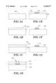
- FIGS. 1A-1Gare diagrammatic representations of a process of forming a silicon oxide structure having a finely calibrated thickness
- FIG. 2is a diagrammatic illustration of one embodiment of a phase shift microlithography mask having a silicon oxide structure formed to a finely calibrated thickness positioned on the mask to thereby achieve a desired phase shift of light traveling therethrough.
- this embodimentdiscloses a process of growing an oxide structure to a finely calibrated thickness on a substrate 100.
- the substrate 100can be a semiconductor substrate upon which the finely calibrated oxide structure is to be formed.
- the substrateis comprised of a light transparent substrate, such as a fused silica glass or quartz material, such as the substrates formed for use in microlithography masks.
- a layer of precursor material 102which is preferably a silicon precursor material and, in this embodiment is comprised of silicon, is deposited to a first thickness.
- the first thickness of the precursor materialis selected so that upon oxidation, the thickness of the resulting oxidized structure is within close tolerances of a desired thickness.
- there is an expansion coefficient of the precursor material 102that allows for relatively accurate determination of the final thickness of the resulting oxide structure as a result of oxidation of the silicon precursor material.
- the precursor material 102is deposited using well-known CVD techniques to an approximate thickness of 425 ⁇ or 546 ⁇ depending on the deep UV wavelength to be used.
- a layer of photoresist 104is then deposited on the layer of precursor material 102.
- the photoresist material 104is deposited using well-known photoresist deposition techniques to thereby allow for selective patterning and removal of the photoresist material 104 to expose a selected region 106 of the precursor material 102.
- a region of the photoresist layer 104 that corresponds to the region 106 of the precursor material 102is transformed by exposure to light from a photolithography mask (not shown) in a manner well known in the art.
- a region of the photoresist material 104is selectively removed using well-known photolithography techniques so as to expose the region 106 of the layer of silicon precursor material 102.
- the exposed region 106 of silicon precursor material 102is ionized to form an ionized or implanted region 107 of the silicon precursor material 102.
- a well-known ion implanterwhich uses argon ions is used to ionize the exposed region 106 such that the concentration of ions is preferably 1 ⁇ 10 14 ions per cubic centimeter or greater.
- the remaining photoresist material 104is then removed in the manner well known in the art.
- the precursor material 102is comprised of the implanted region 107 and two non-implanted regions 110 which are preferably non-implanted silicon regions.
- the non-implanted regions 110are preferably selectively etched so as to remove the non-implanted regions 110 of the precursor material 102 from the substrate 100 leaving the ionized implanted region 107 in the manner shown in FIG. 1F.
- a highly selective wet etchis used that is highly selective so as to remove the non-implanted precursor material 102 forming the regions 110.
- the non-implanted precursor material 102is removed by exposing the silicon precursor material 102 to TMAH (tetra methyl ammonium hydroxide) which selectively removes the unimplanted deposited precursor material 110 without significantly etching the implanted silicon region 107 or the underlying fused silicon glass mask substrate 100.
- TMAHtetra methyl ammonium hydroxide
- tetra methyl ammonium hydroxidecan be used so as to remove substantially all of a 425 ⁇ or 546 ⁇ thick layer of non-implanted regions 110 while limiting the etching of the implanted region 107 of the silicon precursor material to less than one percent of the wavelength of light used for photolithography, i.e., 10 to 12 Angstroms for deep ultraviolet photolithography.
- the non-implanted regions 110 of the precursor material 102can thus be removed with reduced thinning of the implanted region 107 of the silicon precursor material 102.
- the thinning of the implanted region 107is a significant factor in the tolerance to which a structure can be formed.
- the ratio of the removal rates of the non-implanted regions 110 to the implanted silicon region 107is at least approximately 40 to 1. In this way, an implanted silicon precursor structure 107 can be formed on a substrate to have a very specific thickness that is relatively unaffected during the etching process to remove the remaining unimplanted precursor material.
- the remaining implanted silicon precursor structure 107is then oxidized into a silicon oxide structure 112 using well-known oxidation techniques such as wet oxidation. This results in the implanted silicon material being transformed into a silicon oxide (SiO 2 ) material that, in one embodiment, will allow for the transmission of certain wavelengths of light.
- a silicon oxide structure 112can be formed by depositing a layer of precursor silicon of a thickness that is selected so that upon oxidation the resulting thickness after the expansion due to oxidation is within a tolerance of a desired thickness.
- the relatively precise tolerance of thickness of the oxidized structure 112is dependent upon the use of a selective etch to remove the non-implanted regions. The tolerance of the thickness is strongly dependent upon the selectivity of the etchant.
- depositing the silicon precursor material to a thickness of approximately 425 Angstroms or 546 Angstromsresults in a silicon oxide structure of approximately 965 Angstroms or 1240 Angstroms respectively due to the expansion coefficient of silicon upon oxidation of approximately 2.272.
- silicon oxide structure 112has particular adaptability for use in phase shift structures in phase shift lithography masks.
- silicon oxideis transparent to light but has a known effect upon the phase of the light that is traveling therethrough.
- the index of refraction of the material, along with the thickness of the material,dictates the degree of phase shifting that will occur in light that is traveling through such a structure 112.
- phase of the lightis proportional to the change in path of the light through the phase shift structure 112.
- the change in the path of the lightis the result of the light being refracted when entering the phase shift structure 112.
- the degree of refractionis dependent upon the index of refraction which for silicon oxide (SiO 2 ) formed in the above described fashion is approximately 1.46.
- the index of refractionallows for determination of the angle of refraction with which the light travels through the phase shifting structure 112. Consequently, the thickness of the phase shifting structure 112 is directly proportional to the changed path of the light which is, in turn, directly proportional to the change in phase of the light. By being able to precisely control this thickness, the phase of the light travelling through the phase shifting structure 112 can also be precisely controlled.
- the process described in conjunction with FIGS. 1A-1Gresults in the formation of a silicon oxide structure that is approximately 965 or 1240 Angstroms thick. This value has been selected as it is approximately one half of the wavelength of the deep UV light that is used in deep UV photolithography (i.e. deep UV lithography uses light having a wavelength of approximately 2480 or 1930 Angstroms).
- the use of the tetra methyl ammonium hydroxide etch to remove the non-implanted regionsresults in an etching process than removes the non-implanted regions at a rate of 40 times greater than the removal of the implanted regions.
- the thinning of the implanted regions that ultimately results in the silicon oxide structurecan be limited to less than approximately 25 Angstroms or more preferably within approximately 10-12 Angstroms of the desired thickness.
- a very high tolerance phase shift structurecan be formed as will be described in greater detail hereinbelow.
- FIG. 2is a diagram which illustrates one exemplary photolithography mask 200 that incorporates one such silicon oxide phase shift structure 202.
- the photolithography mask 200includes a substrate 204 formed of a light transmitting material, such as fused silica glass, having a uniform thickness.
- An opaque material 206such as chromium, is deposited on an lower surface 210 using well known techniques and is then patterned and etched to form openings 212a, 212b through which light will travel. The light travels through the substrate 204 and then through the openings 212a, 212b in the opaque masking material 206 where the light impinges upon selected regions 214a, 214b of photoresist material 216 positioned on top of a semiconductor substrate 220.
- the openings 212a, 212b in the photolithography mask 200may be positioned so close together that the light emanating from the openings 212a, 212b will illuminate a region 217 of the photoresist material 216 interposed between the regions 214a, 214b to be exposed.
- This problem of unintended illumination of the region 217is particularly pronounced when the light emanating from the openings 212a, 212b of the mask 200 towards the regions 214a, 214b are of the same phase.
- phase shifting structure 202is formed so as to be positioned adjacent the opening 212b.
- the phase shifting structure 202is a silica oxide structure formed using the techniques described above in connection with FIGS. 1A-1G.
- the structure 202can be formed using the process of FIGS. 1A-1G and then the chromium material can be deposited using well-known processing techniques.
- the phase shifting structure 202is formed by depositing a layer of silicon precursor material so that the layer is deposited within the opening 212 to a desired thickness in a manner similar to the manner described above in connection with FIGS. 1A and 1B.
- the layeris then masked and selectively exposed so that a region of silicon precursor material positioned within the opening 212b and immediately adjacent the opening can be ionized in the manner described above in connection with FIGS. 1C and 1D.
- the non-ionized oxide materialis then removed in a manner similar to the manner described above in connection with FIGS. 1E and 1F and the remaining ionized oxide material positioned within the opening 212b is then oxidized in a manner similar to the manner described above in connection with FIG. 1G.
- phase shift structure 202 of a silicon oxide materialcan be formed to a very specific thickness such that the phase of the light travelling through the opening 212b can be shifted by a selected degree. It will be appreciated that the phase shift structure can be formed in the opening 212b in any of a number of manners without departing from the spirit of the present invention.
- a phase shift structure 202can be formed on a phase shift mask 200 within a very close tolerance of a desired thickness.
- the thickness of the structure 202directly affects the degree in which the phase of the light traveling therethrough is shifted.
- it is possible to form structures within a very close tolerancee.g., within 12 Angstroms for deep ultraviolet photolithography, such that the phase of the light emanating from the opening 212b is precisely controlled with respect to the phase of the light emanating from the opening 212a to thereby have the light from each of the openings 212a, 212b to destructively interfere in the region 217 thereby inhibiting development of this portion of the photoresist 216.
- the silicon oxide growth technique of the preferred embodimentsit is possible using the silicon oxide growth technique of the preferred embodiments to form photolithography masks that produce images on photoresist material positioned on a substrate that is much better defined and is of much closer tolerances.
- phase shift structurethat results in an approximately 180 degree phase shift of deep UV photolithography light
- process of the described embodimentcan be adapted to result in any of a number of different phase shifts of any of a number of different wavelengths of light without departing from the spirit of the present invention.
- this processcan be adapted for any of a number of different phase shifting masks including attenuated phase shift masks, rim shift phase shift masks, notch phase shift masks and a number of other phase shift structures known in the art.
- this processcan be adapted to forming structures other than phase shift masks to precise thicknesses without departing from the spirit of the present invention.
Landscapes
- Engineering & Computer Science (AREA)
- Physics & Mathematics (AREA)
- General Physics & Mathematics (AREA)
- Condensed Matter Physics & Semiconductors (AREA)
- Manufacturing & Machinery (AREA)
- Computer Hardware Design (AREA)
- Microelectronics & Electronic Packaging (AREA)
- Power Engineering (AREA)
- Preparing Plates And Mask In Photomechanical Process (AREA)
Abstract
Description
Claims (16)
Priority Applications (2)
| Application Number | Priority Date | Filing Date | Title |
|---|---|---|---|
| US09/385,156US6150277A (en) | 1999-08-30 | 1999-08-30 | Method of making an oxide structure having a finely calibrated thickness |
| US09/498,552US6350547B1 (en) | 1999-08-30 | 2000-02-04 | Oxide structure having a finely calibrated thickness |
Applications Claiming Priority (1)
| Application Number | Priority Date | Filing Date | Title |
|---|---|---|---|
| US09/385,156US6150277A (en) | 1999-08-30 | 1999-08-30 | Method of making an oxide structure having a finely calibrated thickness |
Related Child Applications (1)
| Application Number | Title | Priority Date | Filing Date |
|---|---|---|---|
| US09/498,552DivisionUS6350547B1 (en) | 1999-08-30 | 2000-02-04 | Oxide structure having a finely calibrated thickness |
Publications (1)
| Publication Number | Publication Date |
|---|---|
| US6150277Atrue US6150277A (en) | 2000-11-21 |
Family
ID=23520245
Family Applications (2)
| Application Number | Title | Priority Date | Filing Date |
|---|---|---|---|
| US09/385,156Expired - LifetimeUS6150277A (en) | 1999-08-30 | 1999-08-30 | Method of making an oxide structure having a finely calibrated thickness |
| US09/498,552Expired - Fee RelatedUS6350547B1 (en) | 1999-08-30 | 2000-02-04 | Oxide structure having a finely calibrated thickness |
Family Applications After (1)
| Application Number | Title | Priority Date | Filing Date |
|---|---|---|---|
| US09/498,552Expired - Fee RelatedUS6350547B1 (en) | 1999-08-30 | 2000-02-04 | Oxide structure having a finely calibrated thickness |
Country Status (1)
| Country | Link |
|---|---|
| US (2) | US6150277A (en) |
Cited By (2)
| Publication number | Priority date | Publication date | Assignee | Title |
|---|---|---|---|---|
| US6660635B1 (en) | 2002-03-20 | 2003-12-09 | Taiwan Semiconductor Manufacturing Company | Pre-LDD wet clean recipe to gain channel length scaling margin beyond sub-0.1 μm |
| US20050191856A1 (en)* | 2004-02-27 | 2005-09-01 | Kevin Torek | Method of forming high aspect ratio structures |
Families Citing this family (1)
| Publication number | Priority date | Publication date | Assignee | Title |
|---|---|---|---|---|
| US20050099547A1 (en)* | 2003-11-07 | 2005-05-12 | Vitito Christopher J. | Automobile entertainment system |
Citations (18)
| Publication number | Priority date | Publication date | Assignee | Title |
|---|---|---|---|---|
| US5225034A (en)* | 1992-06-04 | 1993-07-06 | Micron Technology, Inc. | Method of chemical mechanical polishing predominantly copper containing metal layers in semiconductor processing |
| US5234540A (en)* | 1992-04-30 | 1993-08-10 | Submicron Systems, Inc. | Process for etching oxide films in a sealed photochemical reactor |
| US5240522A (en)* | 1991-03-29 | 1993-08-31 | Sumitomo Light Metal Industries, Ltd. | Method of producing hardened aluminum alloy sheets having superior thermal stability |
| US5242524A (en)* | 1990-05-16 | 1993-09-07 | International Business Machines Corporation | Device for detecting an end point in polishing operations |
| US5314843A (en)* | 1992-03-27 | 1994-05-24 | Micron Technology, Inc. | Integrated circuit polishing method |
| US5376483A (en)* | 1993-10-07 | 1994-12-27 | Micron Semiconductor, Inc. | Method of making masks for phase shifting lithography |
| US5407526A (en)* | 1993-06-30 | 1995-04-18 | Intel Corporation | Chemical mechanical polishing slurry delivery and mixing system |
| US5413941A (en)* | 1994-01-06 | 1995-05-09 | Micron Technology, Inc. | Optical end point detection methods in semiconductor planarizing polishing processes |
| US5439553A (en)* | 1994-03-30 | 1995-08-08 | Penn State Research Foundation | Controlled etching of oxides via gas phase reactions |
| US5554939A (en)* | 1992-12-22 | 1996-09-10 | Dainippon Screen Manufacturing Co., Ltd. | Non-destructive measuring sensor for semiconductor wafer and method of manufacturing the same |
| US5576126A (en)* | 1994-09-26 | 1996-11-19 | Micron Technology, Inc. | Phase shifting mask |
| US5637185A (en)* | 1995-03-30 | 1997-06-10 | Rensselaer Polytechnic Institute | Systems for performing chemical mechanical planarization and process for conducting same |
| US5685951A (en)* | 1996-02-15 | 1997-11-11 | Micron Technology, Inc. | Methods and etchants for etching oxides of silicon with low selectivity in a vapor phase system |
| US5781994A (en)* | 1994-12-01 | 1998-07-21 | Commissariate A L'energie Atomique | Process for the micromechanical fabrication of nozzles for liquid jets |
| US5783495A (en)* | 1995-11-13 | 1998-07-21 | Micron Technology, Inc. | Method of wafer cleaning, and system and cleaning solution regarding same |
| US5946595A (en)* | 1997-03-14 | 1999-08-31 | Micron Technology, Inc. | Method of forming a local interconnect between electronic devices on a semiconductor substrate |
| US5965035A (en)* | 1997-10-23 | 1999-10-12 | Applied Materials, Inc. | Self aligned contact etch using difluoromethane and trifluoromethane |
| US5994225A (en)* | 1996-09-10 | 1999-11-30 | United Microelectronics Corp. | Method of etching metal with increased etching selectivity |
Family Cites Families (1)
| Publication number | Priority date | Publication date | Assignee | Title |
|---|---|---|---|---|
| KR0157883B1 (en)* | 1995-05-19 | 1998-12-15 | 문정환 | Phase inversion mask and manufacturing method thereof |
- 1999
- 1999-08-30USUS09/385,156patent/US6150277A/ennot_activeExpired - Lifetime
- 2000
- 2000-02-04USUS09/498,552patent/US6350547B1/ennot_activeExpired - Fee Related
Patent Citations (18)
| Publication number | Priority date | Publication date | Assignee | Title |
|---|---|---|---|---|
| US5242524A (en)* | 1990-05-16 | 1993-09-07 | International Business Machines Corporation | Device for detecting an end point in polishing operations |
| US5240522A (en)* | 1991-03-29 | 1993-08-31 | Sumitomo Light Metal Industries, Ltd. | Method of producing hardened aluminum alloy sheets having superior thermal stability |
| US5314843A (en)* | 1992-03-27 | 1994-05-24 | Micron Technology, Inc. | Integrated circuit polishing method |
| US5234540A (en)* | 1992-04-30 | 1993-08-10 | Submicron Systems, Inc. | Process for etching oxide films in a sealed photochemical reactor |
| US5225034A (en)* | 1992-06-04 | 1993-07-06 | Micron Technology, Inc. | Method of chemical mechanical polishing predominantly copper containing metal layers in semiconductor processing |
| US5554939A (en)* | 1992-12-22 | 1996-09-10 | Dainippon Screen Manufacturing Co., Ltd. | Non-destructive measuring sensor for semiconductor wafer and method of manufacturing the same |
| US5407526A (en)* | 1993-06-30 | 1995-04-18 | Intel Corporation | Chemical mechanical polishing slurry delivery and mixing system |
| US5376483A (en)* | 1993-10-07 | 1994-12-27 | Micron Semiconductor, Inc. | Method of making masks for phase shifting lithography |
| US5413941A (en)* | 1994-01-06 | 1995-05-09 | Micron Technology, Inc. | Optical end point detection methods in semiconductor planarizing polishing processes |
| US5439553A (en)* | 1994-03-30 | 1995-08-08 | Penn State Research Foundation | Controlled etching of oxides via gas phase reactions |
| US5576126A (en)* | 1994-09-26 | 1996-11-19 | Micron Technology, Inc. | Phase shifting mask |
| US5781994A (en)* | 1994-12-01 | 1998-07-21 | Commissariate A L'energie Atomique | Process for the micromechanical fabrication of nozzles for liquid jets |
| US5637185A (en)* | 1995-03-30 | 1997-06-10 | Rensselaer Polytechnic Institute | Systems for performing chemical mechanical planarization and process for conducting same |
| US5783495A (en)* | 1995-11-13 | 1998-07-21 | Micron Technology, Inc. | Method of wafer cleaning, and system and cleaning solution regarding same |
| US5685951A (en)* | 1996-02-15 | 1997-11-11 | Micron Technology, Inc. | Methods and etchants for etching oxides of silicon with low selectivity in a vapor phase system |
| US5994225A (en)* | 1996-09-10 | 1999-11-30 | United Microelectronics Corp. | Method of etching metal with increased etching selectivity |
| US5946595A (en)* | 1997-03-14 | 1999-08-31 | Micron Technology, Inc. | Method of forming a local interconnect between electronic devices on a semiconductor substrate |
| US5965035A (en)* | 1997-10-23 | 1999-10-12 | Applied Materials, Inc. | Self aligned contact etch using difluoromethane and trifluoromethane |
Cited By (5)
| Publication number | Priority date | Publication date | Assignee | Title |
|---|---|---|---|---|
| US6660635B1 (en) | 2002-03-20 | 2003-12-09 | Taiwan Semiconductor Manufacturing Company | Pre-LDD wet clean recipe to gain channel length scaling margin beyond sub-0.1 μm |
| US20050191856A1 (en)* | 2004-02-27 | 2005-09-01 | Kevin Torek | Method of forming high aspect ratio structures |
| US20050287795A1 (en)* | 2004-02-27 | 2005-12-29 | Micron Technology, Inc. | Method of forming high aspect ratio structures |
| US7468323B2 (en) | 2004-02-27 | 2008-12-23 | Micron Technology, Inc. | Method of forming high aspect ratio structures |
| US7932550B2 (en) | 2004-02-27 | 2011-04-26 | Micron Technology, Inc. | Method of forming high aspect ratio structures |
Also Published As
| Publication number | Publication date |
|---|---|
| US6350547B1 (en) | 2002-02-26 |
Similar Documents
| Publication | Publication Date | Title |
|---|---|---|
| US5741625A (en) | Process for forming fine patterns in a semiconductor device utilizing multiple photosensitive film patterns and organic metal-coupled material | |
| US6306547B1 (en) | Photomask and manufacturing method thereof, and exposure method using the photomask | |
| JP2593601B2 (en) | Method for manufacturing phase shift mask | |
| US20080241708A1 (en) | Sub-resolution assist feature of a photomask | |
| US5677111A (en) | Process for production of micropattern utilizing antireflection film | |
| US5292623A (en) | Method for forming integrated circuit devices using a phase shifting mask | |
| JP2641362B2 (en) | Lithography method and manufacturing method of phase shift mask | |
| KR20010017089A (en) | Method of forming minute pattern in semiconductor device | |
| US6569581B2 (en) | Alternating phase shifting masks | |
| US6150277A (en) | Method of making an oxide structure having a finely calibrated thickness | |
| EP1172692A2 (en) | Phase shift mask blank, phase shift mask, and methods of manufacture | |
| US6582856B1 (en) | Simplified method of fabricating a rim phase shift mask | |
| JP3247485B2 (en) | Exposure mask and method of manufacturing the same | |
| US20100081065A1 (en) | Photomask and method of fabricating a photomask | |
| JP4654487B2 (en) | Method for manufacturing phase shift mask | |
| JP3230284B2 (en) | Method for manufacturing phase shift mask | |
| JP3210705B2 (en) | Phase shift photomask | |
| US6348288B1 (en) | Resolution enhancement method for deep quarter micron technology | |
| JPH04291345A (en) | Pattern formation method | |
| KR950004910B1 (en) | Multi-layer photolithography photo etching method | |
| US6723476B2 (en) | Methods of patterning materials; and photomasks | |
| JP3203845B2 (en) | Method of forming gate electrode | |
| KR100318272B1 (en) | Method for forming fine pattern of semiconductor device | |
| US20050266356A1 (en) | Method of forming pattern for semiconductor device | |
| KR100250742B1 (en) | Method of forming line of semiconductor device |
Legal Events
| Date | Code | Title | Description |
|---|---|---|---|
| AS | Assignment | Owner name:MICRON TECHNOLOGY, INC., IDAHO Free format text:ASSIGNMENT OF ASSIGNORS INTEREST;ASSIGNOR:TOREK, KEVIN J.;REEL/FRAME:010211/0705 Effective date:19990824 | |
| STCF | Information on status: patent grant | Free format text:PATENTED CASE | |
| FEPP | Fee payment procedure | Free format text:PAYOR NUMBER ASSIGNED (ORIGINAL EVENT CODE: ASPN); ENTITY STATUS OF PATENT OWNER: LARGE ENTITY | |
| FEPP | Fee payment procedure | Free format text:PAYER NUMBER DE-ASSIGNED (ORIGINAL EVENT CODE: RMPN); ENTITY STATUS OF PATENT OWNER: LARGE ENTITY Free format text:PAYOR NUMBER ASSIGNED (ORIGINAL EVENT CODE: ASPN); ENTITY STATUS OF PATENT OWNER: LARGE ENTITY | |
| FPAY | Fee payment | Year of fee payment:4 | |
| FEPP | Fee payment procedure | Free format text:PAYER NUMBER DE-ASSIGNED (ORIGINAL EVENT CODE: RMPN); ENTITY STATUS OF PATENT OWNER: LARGE ENTITY Free format text:PAYOR NUMBER ASSIGNED (ORIGINAL EVENT CODE: ASPN); ENTITY STATUS OF PATENT OWNER: LARGE ENTITY | |
| FPAY | Fee payment | Year of fee payment:8 | |
| FEPP | Fee payment procedure | Free format text:PAYER NUMBER DE-ASSIGNED (ORIGINAL EVENT CODE: RMPN); ENTITY STATUS OF PATENT OWNER: LARGE ENTITY Free format text:PAYOR NUMBER ASSIGNED (ORIGINAL EVENT CODE: ASPN); ENTITY STATUS OF PATENT OWNER: LARGE ENTITY | |
| FPAY | Fee payment | Year of fee payment:12 | |
| AS | Assignment | Owner name:U.S. BANK NATIONAL ASSOCIATION, AS COLLATERAL AGENT, CALIFORNIA Free format text:SECURITY INTEREST;ASSIGNOR:MICRON TECHNOLOGY, INC.;REEL/FRAME:038669/0001 Effective date:20160426 Owner name:U.S. BANK NATIONAL ASSOCIATION, AS COLLATERAL AGEN Free format text:SECURITY INTEREST;ASSIGNOR:MICRON TECHNOLOGY, INC.;REEL/FRAME:038669/0001 Effective date:20160426 | |
| AS | Assignment | Owner name:MORGAN STANLEY SENIOR FUNDING, INC., AS COLLATERAL AGENT, MARYLAND Free format text:PATENT SECURITY AGREEMENT;ASSIGNOR:MICRON TECHNOLOGY, INC.;REEL/FRAME:038954/0001 Effective date:20160426 Owner name:MORGAN STANLEY SENIOR FUNDING, INC., AS COLLATERAL Free format text:PATENT SECURITY AGREEMENT;ASSIGNOR:MICRON TECHNOLOGY, INC.;REEL/FRAME:038954/0001 Effective date:20160426 | |
| AS | Assignment | Owner name:U.S. BANK NATIONAL ASSOCIATION, AS COLLATERAL AGENT, CALIFORNIA Free format text:CORRECTIVE ASSIGNMENT TO CORRECT THE REPLACE ERRONEOUSLY FILED PATENT #7358718 WITH THE CORRECT PATENT #7358178 PREVIOUSLY RECORDED ON REEL 038669 FRAME 0001. ASSIGNOR(S) HEREBY CONFIRMS THE SECURITY INTEREST;ASSIGNOR:MICRON TECHNOLOGY, INC.;REEL/FRAME:043079/0001 Effective date:20160426 Owner name:U.S. BANK NATIONAL ASSOCIATION, AS COLLATERAL AGEN Free format text:CORRECTIVE ASSIGNMENT TO CORRECT THE REPLACE ERRONEOUSLY FILED PATENT #7358718 WITH THE CORRECT PATENT #7358178 PREVIOUSLY RECORDED ON REEL 038669 FRAME 0001. ASSIGNOR(S) HEREBY CONFIRMS THE SECURITY INTEREST;ASSIGNOR:MICRON TECHNOLOGY, INC.;REEL/FRAME:043079/0001 Effective date:20160426 | |
| AS | Assignment | Owner name:JPMORGAN CHASE BANK, N.A., AS COLLATERAL AGENT, ILLINOIS Free format text:SECURITY INTEREST;ASSIGNORS:MICRON TECHNOLOGY, INC.;MICRON SEMICONDUCTOR PRODUCTS, INC.;REEL/FRAME:047540/0001 Effective date:20180703 Owner name:JPMORGAN CHASE BANK, N.A., AS COLLATERAL AGENT, IL Free format text:SECURITY INTEREST;ASSIGNORS:MICRON TECHNOLOGY, INC.;MICRON SEMICONDUCTOR PRODUCTS, INC.;REEL/FRAME:047540/0001 Effective date:20180703 | |
| AS | Assignment | Owner name:MICRON TECHNOLOGY, INC., IDAHO Free format text:RELEASE BY SECURED PARTY;ASSIGNOR:U.S. BANK NATIONAL ASSOCIATION, AS COLLATERAL AGENT;REEL/FRAME:047243/0001 Effective date:20180629 | |
| AS | Assignment | Owner name:MICRON TECHNOLOGY, INC., IDAHO Free format text:RELEASE BY SECURED PARTY;ASSIGNOR:MORGAN STANLEY SENIOR FUNDING, INC., AS COLLATERAL AGENT;REEL/FRAME:050937/0001 Effective date:20190731 | |
| AS | Assignment | Owner name:MICRON SEMICONDUCTOR PRODUCTS, INC., IDAHO Free format text:RELEASE BY SECURED PARTY;ASSIGNOR:JPMORGAN CHASE BANK, N.A., AS COLLATERAL AGENT;REEL/FRAME:051028/0001 Effective date:20190731 Owner name:MICRON TECHNOLOGY, INC., IDAHO Free format text:RELEASE BY SECURED PARTY;ASSIGNOR:JPMORGAN CHASE BANK, N.A., AS COLLATERAL AGENT;REEL/FRAME:051028/0001 Effective date:20190731 |