US6148435A - Optimized programming/erase parameters for programmable devices - Google Patents
Optimized programming/erase parameters for programmable devicesDownload PDFInfo
- Publication number
- US6148435A US6148435AUS08/998,090US99809097AUS6148435AUS 6148435 AUS6148435 AUS 6148435AUS 99809097 AUS99809097 AUS 99809097AUS 6148435 AUS6148435 AUS 6148435A
- Authority
- US
- United States
- Prior art keywords
- programming
- optimized
- programmable device
- parameter
- erase
- Prior art date
- Legal status (The legal status is an assumption and is not a legal conclusion. Google has not performed a legal analysis and makes no representation as to the accuracy of the status listed.)
- Expired - Lifetime
Links
- 238000000034methodMethods0.000claimsabstractdescription36
- 230000015654memoryEffects0.000description11
- 238000004519manufacturing processMethods0.000description5
- 238000012795verificationMethods0.000description2
- 238000003491arrayMethods0.000description1
- 230000005684electric fieldEffects0.000description1
- 238000012986modificationMethods0.000description1
- 230000004048modificationEffects0.000description1
Images


Classifications
- G—PHYSICS
- G11—INFORMATION STORAGE
- G11C—STATIC STORES
- G11C16/00—Erasable programmable read-only memories
- G11C16/02—Erasable programmable read-only memories electrically programmable
- G11C16/06—Auxiliary circuits, e.g. for writing into memory
- G11C16/10—Programming or data input circuits
- G—PHYSICS
- G11—INFORMATION STORAGE
- G11C—STATIC STORES
- G11C16/00—Erasable programmable read-only memories
- G11C16/02—Erasable programmable read-only memories electrically programmable
- G11C16/06—Auxiliary circuits, e.g. for writing into memory
- G11C16/10—Programming or data input circuits
- G11C16/14—Circuits for erasing electrically, e.g. erase voltage switching circuits
Definitions
- the present inventionrelates generally to programmable devices and, more particularly, to the programming and erasing of such devices.
- Programmable devicessuch as electrically erasable programmable read only memories (EEPROMs), flash memories, programmable logic devices (PLDs), complex programmable logic devices (CPLDs), programmable array logic (PAL), field programmable gate arrays (FPGAs), etc., typically include non-volatile memory elements which can be programmed or erased under the control of appropriate programming or erase voltages.
- the programming or erase voltageis typically applied to the non-volatile memory element for a period of time (a programming or erase pulse width) sufficient to achieve the desired programming or erasing of the memory cell.
- a programming or erase pulse widthe.g., as may be specified by a manufacture of the programmable device.
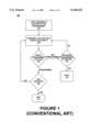
- FIG. 1illustrates a conventional programming operation 100 for a programmable device.
- the operationbegins at step 102 where the address of the location to be programmed is loaded into the programming unit. Then, at step 104, that location is programmed according to the fixed pulse width, e.g., as may be specified by the manufacture of the programmable device.
- the programming stepis verified at step 106. During verification, the addressed location is checked to determine whether programming was successful. If so, the check is made at step 108 to determine whether this was the last location in the programmable device to be programmed. When all such locations have been programmed, the process quits at step 110.
- the fixed programming pulse widthmay be inadequate to assure programming of all locations in the programmable device.
- the fixed programming pulse widthmay exceed the time necessary to adequately program the non-volatile memory cells. Either case presents a problem. For example, where the programming pulse width is not long enough, otherwise useful devices may be rejected because they fail repeated programming attempts.
- the programming pulse widthis to long, repeated programming and erase operations may cause early failure of the memory cells (e.g., due to oxide break down in the presence of strong electric fields caused by the programming and/or erase voltages).
- the use of fixed programming parameters(such as pulse widths) for programmable devices presents a less than ideal solution.
- the present inventionprovides a optimized programming or erase parameter for a programmable device.
- the optimized programming or erase parameter(s)is (are) determined for the programmable device and that parameter (or those parameters) is (are) stored in the programmable device.
- the optimized parameter (or parameters)is (are) read from the programmable device and used in the programming or erase process.
- the present inventionprovides a method which includes storing an optimized parameter for a programmable device within the programmable device.
- the methodmay further include programming or erasing the programmable device according to the optimized parameter.
- the optimized parametermay be a pulse width.
- the methodmay include reading an optimized parameter from the programmable device and programming or erasing the programmable device according to the optimized parameter.
- the optimized parametermay be a pulse width.
- a programmable devicehas stored therein an optimized programming and/or erase parameter, such as a programming and/or erase pulse width.
- FIG. 1illustrates an conventional programming operation for a programmable device using a fixed programming pulse width
- FIG. 2illustrates one embodiment of the present invention wherein optimized programming and/or erase parameters are programmed into a programmable device
- FIG. 3illustrates an exemplary routine for utilizing a stored optimized programming and/or erase parameter according to an embodiment of the present invention.
- the present inventionprovides a optimized programming or erase parameter for a programmable device. After manufacture, but prior to shipping, the optimized programming or erase parameter is determined for the programmable device and that parameter (or parameters) is (are) stored in the programmable device. When the programmable device is to be programmed or erased, the optimized parameter (or parameters) is (are) read from the programmable device and used in the programming or erase process.
- the present inventionprovides a method which includes storing an optimized programming parameter for a programmable device within the programmable device.
- the methodmay further include programming the programmable device according to the optimized programming parameter.
- the programming parametermay be a programming pulse width.
- the methodmay include storing an optimized erase parameter within the programmable device.
- the programming and erase parametermay be the same parameter, for example an optimized pulse width. Where an optimized erase parameter is used, the optimized erase parameter may be read prior to an erase operation and the erase operation may then be performed according to that optimized parameter.
- a programmable devicehas stored therein an optimized parameter, such as a programming or erase parameter (e.g., a pulse width and/or a voltage level).
- a programming or erase parametere.g., a pulse width and/or a voltage level.
- FIG. 2illustrates one embodiment of the present invention as a routine 200 for optimizing the programming and/or erasing of a programmable device.
- one or more optimized programming and/or erase parameters for the programmable deviceare stored in appropriate storage locations (e.g., registers or other memory locations) within the programmable device. Such storing is typically performed prior to shipping the programmable device to customers, however, in some cases the storing may be performed after a programmable device has been received by a customer.
- the optimized programming and/or erase parameterse.g., which may be pulse widths, may be determined by the manufacturer of the programmable device (or in some cases by the customer who ultimately uses the programmable device).
- Such a determinationmay be made, for example, by testing various programming and/or erase parameters with randomly selected units of a lot of programmable devices. When optimized parameters have been determined, each of the programmable devices of the tested batch or lot may be programmed with these parameters prior to shipping.
- the optimized programming and/or erase parametersare read by appropriate programming and/or erasing units and the programmable device is then programmed or erased according to the optimized parameter(s). Minor modifications to the software and/or firmware of conventional programming devices may be required to allow these devices to read the optimized programming and/or erase parameters prior to beginning a programming or erase operation.
- the optimized programming and/or erase parameter(s)may include a pulse width.
- FIG. 3illustrates a routine 300 for programming and/or erasing a programmable device according to one embodiment of the present invention.
- the optimized programming and/or erase parameter(s)e.g., a pulse width
- the optimized parameter(s)may have been previously stored prior to shipping the programmable device.
- the address of the location(s) to be programmed or eraseis (are) loaded. It should be appreciated that step 304 may be carried out prior to step 302 in some embodiments.
- the programming or erase operationis conducted at 306.
- This operationis conducted according to the optimized parameter from step 302.
- a programming voltagemay be applied for a period of time corresponding to an optimized programming pulse width stored in and read from the programmable device.
- an appropriate erase voltagemay be applied for a period of time equivalent to an optimized erase pulse width stored in and read from the programmable device.
- a variety of optimized programming and/or erase parametersmay have been read at step 302, for example, optimized voltages and pulse widths. In such a case, each of these optimized parameters may be utilized at step 306.
- the programming or erase operationis verified at step 308. If the verification determines that the programming or erase operation was successful, a check is made at step 310 to determine if this was the last such operation required. Multiple programming and/or erase operations may be performed until all of the locations to be programmed and/or erased have been successfully programmed and/or erased. When all such locations have been verified, the process quits at step 312.
- the partmay fail the programming or erase operation at step 314.
- no looping operation to attempt additional programming or erasing of an addressed locationis carried out. Since the use of optimized programming and/or erase parameters should have accomplished the desired programming or erase operation, a failure likely represents a true failure of the programmable device and the part should not be used. In other embodiments, it may be desirable to provide multiple attempts to complete the programming or erasing of a particular location, for example, where there is reason to suspected that the programming or erase operation may have been terminated prematurely (e.g., due to a power failure or other event).
- the present methodsespecially where branches in the programming/erase operation loop have been eliminated, ease the overall burden on the software for such operations. Thus, faster programming and/or erase times may be experienced.
- the present methodsalso allow a manufacturer to tailor pulse widths and/or other parameters (e.g., voltage levels) for programming or erase operations for individual programmable devices or lots of devices. Such methods may be especially useful for electrically erasable programmable read only memory cells and/or flash memory cells of programmable devices where successive programming and /or erase pulses must typically be longer than a first programming or erase pulse, in order to achieve programming or erasing of the cells.
- a recordcould be kept (e.g., stored in the programmable device in an appropriate register or other memory location) of the number of times a particular device has been subjected to programming and/or erase cycles. Then, an appropriate (and previously stored, e.g., at the time of manufacture or even at the time of ultimate customer use) optimized programming and/or erase parameter could be read from one of a number of storage locations within the programmable device, based on the cycle number stored in the programmable device. In other words, different optimized programming and/or erase parameters may be stored at different locations within the programmable device and appropriate ones of these different programming and/or erase parameters selected and used at various times during the life cycle of programmable device.
Landscapes
- Read Only Memory (AREA)
Abstract
Description
Claims (22)
Priority Applications (1)
| Application Number | Priority Date | Filing Date | Title |
|---|---|---|---|
| US08/998,090US6148435A (en) | 1997-12-24 | 1997-12-24 | Optimized programming/erase parameters for programmable devices |
Applications Claiming Priority (1)
| Application Number | Priority Date | Filing Date | Title |
|---|---|---|---|
| US08/998,090US6148435A (en) | 1997-12-24 | 1997-12-24 | Optimized programming/erase parameters for programmable devices |
Publications (1)
| Publication Number | Publication Date |
|---|---|
| US6148435Atrue US6148435A (en) | 2000-11-14 |
Family
ID=25544738
Family Applications (1)
| Application Number | Title | Priority Date | Filing Date |
|---|---|---|---|
| US08/998,090Expired - LifetimeUS6148435A (en) | 1997-12-24 | 1997-12-24 | Optimized programming/erase parameters for programmable devices |
Country Status (1)
| Country | Link |
|---|---|
| US (1) | US6148435A (en) |
Cited By (18)
| Publication number | Priority date | Publication date | Assignee | Title |
|---|---|---|---|---|
| US20030067809A1 (en)* | 2001-10-09 | 2003-04-10 | Micron Technology, Inc. | Faster method of erasing flash memory |
| US20050162909A1 (en)* | 2001-10-05 | 2005-07-28 | Micron Technology, Inc. | Flash memory device with a variable erase pulse |
| US20050278464A1 (en)* | 2004-05-13 | 2005-12-15 | Claseman George R | Multiple state configuration method |
| WO2006021838A1 (en)* | 2004-08-27 | 2006-03-02 | Nokia Corporation | Method and system for accessing performance parameters in memory devices |
| US20060158938A1 (en)* | 2005-01-19 | 2006-07-20 | Saifun Semiconductors, Ltd. | Method, circuit and systems for erasing one or more non-volatile memory cells |
| US20070168625A1 (en)* | 2006-01-18 | 2007-07-19 | Cornwell Michael J | Interleaving policies for flash memory |
| US20070165461A1 (en)* | 2006-01-18 | 2007-07-19 | Cornwell Michael J | Disabling faulty flash memory dies |
| US20070174642A1 (en)* | 2006-01-25 | 2007-07-26 | Cornwell Michael J | Reporting flash memory operating voltages |
| US20070174641A1 (en)* | 2006-01-25 | 2007-07-26 | Cornwell Michael J | Adjusting power supplies for data storage devices |
| US20080288712A1 (en)* | 2007-04-25 | 2008-11-20 | Cornwell Michael J | Accessing metadata with an external host |
| US7535765B2 (en) | 2004-12-09 | 2009-05-19 | Saifun Semiconductors Ltd. | Non-volatile memory device and method for reading cells |
| US7605579B2 (en) | 2006-09-18 | 2009-10-20 | Saifun Semiconductors Ltd. | Measuring and controlling current consumption and output current of charge pumps |
| US7638835B2 (en) | 2006-02-28 | 2009-12-29 | Saifun Semiconductors Ltd. | Double density NROM with nitride strips (DDNS) |
| US7743230B2 (en) | 2003-01-31 | 2010-06-22 | Saifun Semiconductors Ltd. | Memory array programming circuit and a method for using the circuit |
| US7808818B2 (en) | 2006-01-12 | 2010-10-05 | Saifun Semiconductors Ltd. | Secondary injection for NROM |
| US7861122B2 (en) | 2006-01-27 | 2010-12-28 | Apple Inc. | Monitoring health of non-volatile memory |
| US7913032B1 (en) | 2007-04-25 | 2011-03-22 | Apple Inc. | Initiating memory wear leveling |
| US8988940B2 (en) | 2012-07-31 | 2015-03-24 | International Business Machines Corporation | Structure and method for narrowing voltage threshold distribution in non-volatile memories |
Citations (18)
| Publication number | Priority date | Publication date | Assignee | Title |
|---|---|---|---|---|
| US5257225A (en)* | 1992-03-12 | 1993-10-26 | Micron Technology, Inc. | Method for programming programmable devices by utilizing single or multiple pulses varying in pulse width and amplitude |
| US5268870A (en)* | 1988-06-08 | 1993-12-07 | Eliyahou Harari | Flash EEPROM system and intelligent programming and erasing methods therefor |
| US5272388A (en)* | 1992-06-09 | 1993-12-21 | Actel Corporation | High-yield methods for programming antifuses |
| US5397939A (en)* | 1991-07-31 | 1995-03-14 | Quicklogic Corporation | Programming of antifuses |
| US5428568A (en)* | 1991-10-30 | 1995-06-27 | Mitsubishi Denki Kabushiki Kaisha | Electrically erasable and programmable non-volatile memory device and a method of operating the same |
| US5490109A (en)* | 1994-06-28 | 1996-02-06 | Intel Corporation | Method and apparatus for preventing over-erasure of flash EEPROM memory devices |
| US5499191A (en)* | 1992-06-15 | 1996-03-12 | Minc Incorporated | Multi-level logic optimization in programmable logic devices |
| US5532959A (en)* | 1991-09-27 | 1996-07-02 | Nec Corporation | Electrically erasable and programmable read only memory device equipped with inspection circuit for threshold levels of memory cells |
| US5621685A (en)* | 1994-10-17 | 1997-04-15 | Sandisk Corporation | Programmable power generation circuit for flash EEPROM memory systems |
| US5661412A (en)* | 1995-10-10 | 1997-08-26 | Quicklogic Corporation | Reducing programming time of a field programmable gate array employing antifuses |
| US5729489A (en)* | 1995-12-14 | 1998-03-17 | Intel Corporation | Programming flash memory using predictive learning methods |
| US5734868A (en)* | 1995-08-09 | 1998-03-31 | Curd; Derek R. | Efficient in-system programming structure and method for non-volatile programmable logic devices |
| US5777887A (en)* | 1995-05-12 | 1998-07-07 | Crosspoint Solutions, Inc. | FPGA redundancy |
| US5815404A (en)* | 1995-10-16 | 1998-09-29 | Xilinx, Inc. | Method and apparatus for obtaining and using antifuse testing information to increase programmable device yield |
| US5873113A (en)* | 1996-09-24 | 1999-02-16 | Altera Corporation | System and method for programming eprom cells using shorter duration pulse(s) in repeating the programming process of a particular cell |
| US5880996A (en)* | 1995-07-28 | 1999-03-09 | Micron Technology, Inc. | Memory system having non-volatile data storage structure for memory control parameters and method |
| US5889701A (en)* | 1998-06-18 | 1999-03-30 | Xilinx, Inc. | Method and apparatus for selecting optimum levels for in-system programmable charge pumps |
| US5901194A (en)* | 1995-07-28 | 1999-05-04 | Micron Technologies, Inc | Timer circuit with programmable decode circuitry |
- 1997
- 1997-12-24USUS08/998,090patent/US6148435A/ennot_activeExpired - Lifetime
Patent Citations (18)
| Publication number | Priority date | Publication date | Assignee | Title |
|---|---|---|---|---|
| US5268870A (en)* | 1988-06-08 | 1993-12-07 | Eliyahou Harari | Flash EEPROM system and intelligent programming and erasing methods therefor |
| US5397939A (en)* | 1991-07-31 | 1995-03-14 | Quicklogic Corporation | Programming of antifuses |
| US5532959A (en)* | 1991-09-27 | 1996-07-02 | Nec Corporation | Electrically erasable and programmable read only memory device equipped with inspection circuit for threshold levels of memory cells |
| US5428568A (en)* | 1991-10-30 | 1995-06-27 | Mitsubishi Denki Kabushiki Kaisha | Electrically erasable and programmable non-volatile memory device and a method of operating the same |
| US5257225A (en)* | 1992-03-12 | 1993-10-26 | Micron Technology, Inc. | Method for programming programmable devices by utilizing single or multiple pulses varying in pulse width and amplitude |
| US5272388A (en)* | 1992-06-09 | 1993-12-21 | Actel Corporation | High-yield methods for programming antifuses |
| US5499191A (en)* | 1992-06-15 | 1996-03-12 | Minc Incorporated | Multi-level logic optimization in programmable logic devices |
| US5490109A (en)* | 1994-06-28 | 1996-02-06 | Intel Corporation | Method and apparatus for preventing over-erasure of flash EEPROM memory devices |
| US5621685A (en)* | 1994-10-17 | 1997-04-15 | Sandisk Corporation | Programmable power generation circuit for flash EEPROM memory systems |
| US5777887A (en)* | 1995-05-12 | 1998-07-07 | Crosspoint Solutions, Inc. | FPGA redundancy |
| US5880996A (en)* | 1995-07-28 | 1999-03-09 | Micron Technology, Inc. | Memory system having non-volatile data storage structure for memory control parameters and method |
| US5901194A (en)* | 1995-07-28 | 1999-05-04 | Micron Technologies, Inc | Timer circuit with programmable decode circuitry |
| US5734868A (en)* | 1995-08-09 | 1998-03-31 | Curd; Derek R. | Efficient in-system programming structure and method for non-volatile programmable logic devices |
| US5661412A (en)* | 1995-10-10 | 1997-08-26 | Quicklogic Corporation | Reducing programming time of a field programmable gate array employing antifuses |
| US5815404A (en)* | 1995-10-16 | 1998-09-29 | Xilinx, Inc. | Method and apparatus for obtaining and using antifuse testing information to increase programmable device yield |
| US5729489A (en)* | 1995-12-14 | 1998-03-17 | Intel Corporation | Programming flash memory using predictive learning methods |
| US5873113A (en)* | 1996-09-24 | 1999-02-16 | Altera Corporation | System and method for programming eprom cells using shorter duration pulse(s) in repeating the programming process of a particular cell |
| US5889701A (en)* | 1998-06-18 | 1999-03-30 | Xilinx, Inc. | Method and apparatus for selecting optimum levels for in-system programmable charge pumps |
Cited By (39)
| Publication number | Priority date | Publication date | Assignee | Title |
|---|---|---|---|---|
| US7167399B2 (en)* | 2001-10-05 | 2007-01-23 | Micron Technology, Inc. | Flash memory device with a variable erase pulse |
| US20050162909A1 (en)* | 2001-10-05 | 2005-07-28 | Micron Technology, Inc. | Flash memory device with a variable erase pulse |
| US20030067809A1 (en)* | 2001-10-09 | 2003-04-10 | Micron Technology, Inc. | Faster method of erasing flash memory |
| US20060004960A1 (en)* | 2001-10-09 | 2006-01-05 | Micron Technology, Inc. | Faster method of erasing flash memory |
| US20060002194A1 (en)* | 2001-10-09 | 2006-01-05 | Micron Technology, Inc. | Faster method of erasing flash memory |
| US7061810B2 (en) | 2001-10-09 | 2006-06-13 | Micron Technology, Inc. | Erasing flash memory without pre-programming the flash memory before erasing |
| US7061811B2 (en) | 2001-10-09 | 2006-06-13 | Micron Technology, Inc. | Faster method of erasing flash memory |
| US20070223285A1 (en)* | 2001-10-09 | 2007-09-27 | Micron Technology, Inc. | Method of erasing flash memory |
| US7554852B2 (en) | 2001-10-09 | 2009-06-30 | Micron Technology, Inc. | Method of erasing flash memory with pre-programming memory cells only in the presence of a cell leakage |
| US7233525B2 (en) | 2001-10-09 | 2007-06-19 | Micron Technology, Inc. | Method of converting contents of flash memory cells in the presence of leakage |
| US7743230B2 (en) | 2003-01-31 | 2010-06-22 | Saifun Semiconductors Ltd. | Memory array programming circuit and a method for using the circuit |
| US20050278464A1 (en)* | 2004-05-13 | 2005-12-15 | Claseman George R | Multiple state configuration method |
| WO2006021838A1 (en)* | 2004-08-27 | 2006-03-02 | Nokia Corporation | Method and system for accessing performance parameters in memory devices |
| US20060044926A1 (en)* | 2004-08-27 | 2006-03-02 | Nokia Corporation | Method and system for accessing performance parameters in memory devices |
| US7535765B2 (en) | 2004-12-09 | 2009-05-19 | Saifun Semiconductors Ltd. | Non-volatile memory device and method for reading cells |
| US20060158938A1 (en)* | 2005-01-19 | 2006-07-20 | Saifun Semiconductors, Ltd. | Method, circuit and systems for erasing one or more non-volatile memory cells |
| US7468926B2 (en) | 2005-01-19 | 2008-12-23 | Saifun Semiconductors Ltd. | Partial erase verify |
| EP1684307A1 (en)* | 2005-01-19 | 2006-07-26 | Saifun Semiconductors Ltd. | Method, circuit and systems for erasing one or more non-volatile memory cells |
| US20060181934A1 (en)* | 2005-01-19 | 2006-08-17 | Saifun Semiconductors, Ltd. | Methods for preventing fixed pattern programming |
| US7369440B2 (en) | 2005-01-19 | 2008-05-06 | Saifun Semiconductors Ltd. | Method, circuit and systems for erasing one or more non-volatile memory cells |
| US7808818B2 (en) | 2006-01-12 | 2010-10-05 | Saifun Semiconductors Ltd. | Secondary injection for NROM |
| US20100002512A1 (en)* | 2006-01-18 | 2010-01-07 | Cornwell Michael J | Disabling faulty flash memory dies |
| US20070168625A1 (en)* | 2006-01-18 | 2007-07-19 | Cornwell Michael J | Interleaving policies for flash memory |
| US20070165461A1 (en)* | 2006-01-18 | 2007-07-19 | Cornwell Michael J | Disabling faulty flash memory dies |
| US8055959B2 (en) | 2006-01-18 | 2011-11-08 | Apple Inc. | Disabling faulty flash memory dies |
| US7609561B2 (en) | 2006-01-18 | 2009-10-27 | Apple Inc. | Disabling faulty flash memory dies |
| US7793059B2 (en) | 2006-01-18 | 2010-09-07 | Apple Inc. | Interleaving policies for flash memory |
| US20070174641A1 (en)* | 2006-01-25 | 2007-07-26 | Cornwell Michael J | Adjusting power supplies for data storage devices |
| US7702935B2 (en) | 2006-01-25 | 2010-04-20 | Apple Inc. | Reporting flash memory operating voltages |
| US20070174642A1 (en)* | 2006-01-25 | 2007-07-26 | Cornwell Michael J | Reporting flash memory operating voltages |
| US8171318B2 (en) | 2006-01-25 | 2012-05-01 | Apple Inc. | Reporting flash memory operating voltages |
| US7861122B2 (en) | 2006-01-27 | 2010-12-28 | Apple Inc. | Monitoring health of non-volatile memory |
| US7638835B2 (en) | 2006-02-28 | 2009-12-29 | Saifun Semiconductors Ltd. | Double density NROM with nitride strips (DDNS) |
| US7605579B2 (en) | 2006-09-18 | 2009-10-20 | Saifun Semiconductors Ltd. | Measuring and controlling current consumption and output current of charge pumps |
| US20080288712A1 (en)* | 2007-04-25 | 2008-11-20 | Cornwell Michael J | Accessing metadata with an external host |
| US7913032B1 (en) | 2007-04-25 | 2011-03-22 | Apple Inc. | Initiating memory wear leveling |
| US8677057B1 (en) | 2007-04-25 | 2014-03-18 | Apple Inc. | Initiating memory wear leveling |
| US8745328B2 (en) | 2007-04-25 | 2014-06-03 | Apple Inc. | Updating error correction codes for data blocks |
| US8988940B2 (en) | 2012-07-31 | 2015-03-24 | International Business Machines Corporation | Structure and method for narrowing voltage threshold distribution in non-volatile memories |
Similar Documents
| Publication | Publication Date | Title |
|---|---|---|
| US6148435A (en) | Optimized programming/erase parameters for programmable devices | |
| KR101285576B1 (en) | Method and apparatus for programming/erasing a non-volatile memory | |
| US7251190B2 (en) | Non-volatile semiconductor memory device | |
| US5523972A (en) | Method and apparatus for verifying the programming of multi-level flash EEPROM memory | |
| US5237535A (en) | Method of repairing overerased cells in a flash memory | |
| US6272586B1 (en) | Memory system having programmable control parameters | |
| US6981188B2 (en) | Non-volatile memory device with self test | |
| US5751647A (en) | On-chip memory redundancy circuitry for programmable non-volatile memories, and methods for programming same | |
| KR100315321B1 (en) | Nonvolatile semiconductor memory device and erase verify method therefor | |
| US7047455B2 (en) | Memory with element redundancy | |
| KR100611825B1 (en) | Programming method and device | |
| US7277981B2 (en) | Scratch control memory array in a flash memory device | |
| US7437625B2 (en) | Memory with element redundancy | |
| US5621738A (en) | Method for programming flash EEPROM devices | |
| US20070223276A1 (en) | Non-volatile memory wih controlled program/erase | |
| US5751944A (en) | Non-volatile memory system having automatic cycling test function | |
| EP1233421B1 (en) | Method for refreshing stored data in an electrically erasable and programmable non-volatile memory | |
| EP1750277A1 (en) | Configuration of a multi-level flash memory device | |
| US5673228A (en) | Integrated circuit having an EEPROM, semiconductor wafer provided with such integrated circuits, and method of testing such a semiconductor wafer | |
| US6462990B1 (en) | Post erase repair to enhance performance in a flash memory | |
| JP2004533697A (en) | I/O splitting system and method for mitigating band-to-band tunneling current during erase - Patents.com | |
| JPH09213093A (en) | NONVOLATILE SEMICONDUCTOR MEMORY DEVICE, TEST METHOD AND TRIMING METHOD THEREOF | |
| EP1782426B1 (en) | Self-adaptive program delay circuitry for programmable memories | |
| KR19990042162A (en) | Nonvolatile Memory Device And Its Program Method |
Legal Events
| Date | Code | Title | Description |
|---|---|---|---|
| AS | Assignment | Owner name:CYPRESS SEMICONDUCTOR CORPORATION, CALIFORNIA Free format text:ASSIGNMENT OF ASSIGNORS INTEREST;ASSIGNOR:BETTMAN, ROGER;REEL/FRAME:008938/0962 Effective date:19971224 | |
| STCF | Information on status: patent grant | Free format text:PATENTED CASE | |
| FEPP | Fee payment procedure | Free format text:PAYOR NUMBER ASSIGNED (ORIGINAL EVENT CODE: ASPN); ENTITY STATUS OF PATENT OWNER: LARGE ENTITY | |
| FPAY | Fee payment | Year of fee payment:4 | |
| FEPP | Fee payment procedure | Free format text:PAYOR NUMBER ASSIGNED (ORIGINAL EVENT CODE: ASPN); ENTITY STATUS OF PATENT OWNER: LARGE ENTITY Free format text:PAYER NUMBER DE-ASSIGNED (ORIGINAL EVENT CODE: RMPN); ENTITY STATUS OF PATENT OWNER: LARGE ENTITY | |
| FPAY | Fee payment | Year of fee payment:8 | |
| FPAY | Fee payment | Year of fee payment:12 | |
| AS | Assignment | Owner name:MORGAN STANLEY SENIOR FUNDING, INC., NEW YORK Free format text:SECURITY INTEREST;ASSIGNORS:CYPRESS SEMICONDUCTOR CORPORATION;SPANSION LLC;REEL/FRAME:035240/0429 Effective date:20150312 | |
| AS | Assignment | Owner name:CYPRESS SEMICONDUCTOR CORPORATION, CALIFORNIA Free format text:PARTIAL RELEASE OF SECURITY INTEREST IN PATENTS;ASSIGNOR:MORGAN STANLEY SENIOR FUNDING, INC., AS COLLATERAL AGENT;REEL/FRAME:039708/0001 Effective date:20160811 Owner name:SPANSION LLC, CALIFORNIA Free format text:PARTIAL RELEASE OF SECURITY INTEREST IN PATENTS;ASSIGNOR:MORGAN STANLEY SENIOR FUNDING, INC., AS COLLATERAL AGENT;REEL/FRAME:039708/0001 Effective date:20160811 | |
| AS | Assignment | Owner name:MONTEREY RESEARCH, LLC, CALIFORNIA Free format text:ASSIGNMENT OF ASSIGNORS INTEREST;ASSIGNOR:CYPRESS SEMICONDUCTOR CORPORATION;REEL/FRAME:040911/0238 Effective date:20160811 | |
| AS | Assignment | Owner name:MORGAN STANLEY SENIOR FUNDING, INC., NEW YORK Free format text:CORRECTIVE ASSIGNMENT TO CORRECT THE 8647899 PREVIOUSLY RECORDED ON REEL 035240 FRAME 0429. ASSIGNOR(S) HEREBY CONFIRMS THE SECURITY INTERST;ASSIGNORS:CYPRESS SEMICONDUCTOR CORPORATION;SPANSION LLC;REEL/FRAME:058002/0470 Effective date:20150312 |