US6147665A - Column driver output amplifier with low quiescent power consumption for field emission display devices - Google Patents
Column driver output amplifier with low quiescent power consumption for field emission display devicesDownload PDFInfo
- Publication number
- US6147665A US6147665AUS09/162,823US16282398AUS6147665AUS 6147665 AUS6147665 AUS 6147665AUS 16282398 AUS16282398 AUS 16282398AUS 6147665 AUS6147665 AUS 6147665A
- Authority
- US
- United States
- Prior art keywords
- voltage signal
- output
- current
- circuit
- input voltage
- Prior art date
- Legal status (The legal status is an assumption and is not a legal conclusion. Google has not performed a legal analysis and makes no representation as to the accuracy of the status listed.)
- Expired - Lifetime
Links
- 230000008878couplingEffects0.000abstract2
- 238000010168coupling processMethods0.000abstract2
- 238000005859coupling reactionMethods0.000abstract2
- 238000006243chemical reactionMethods0.000abstract1
- 238000012544monitoring processMethods0.000abstract1
Images


Classifications
- G—PHYSICS
- G09—EDUCATION; CRYPTOGRAPHY; DISPLAY; ADVERTISING; SEALS
- G09G—ARRANGEMENTS OR CIRCUITS FOR CONTROL OF INDICATING DEVICES USING STATIC MEANS TO PRESENT VARIABLE INFORMATION
- G09G3/00—Control arrangements or circuits, of interest only in connection with visual indicators other than cathode-ray tubes
- G09G3/20—Control arrangements or circuits, of interest only in connection with visual indicators other than cathode-ray tubes for presentation of an assembly of a number of characters, e.g. a page, by composing the assembly by combination of individual elements arranged in a matrix no fixed position being assigned to or needed to be assigned to the individual characters or partial characters
- G09G3/22—Control arrangements or circuits, of interest only in connection with visual indicators other than cathode-ray tubes for presentation of an assembly of a number of characters, e.g. a page, by composing the assembly by combination of individual elements arranged in a matrix no fixed position being assigned to or needed to be assigned to the individual characters or partial characters using controlled light sources
- G—PHYSICS
- G09—EDUCATION; CRYPTOGRAPHY; DISPLAY; ADVERTISING; SEALS
- G09G—ARRANGEMENTS OR CIRCUITS FOR CONTROL OF INDICATING DEVICES USING STATIC MEANS TO PRESENT VARIABLE INFORMATION
- G09G2310/00—Command of the display device
- G09G2310/02—Addressing, scanning or driving the display screen or processing steps related thereto
- G09G2310/0264—Details of driving circuits
- G09G2310/0275—Details of drivers for data electrodes, other than drivers for liquid crystal, plasma or OLED displays, not related to handling digital grey scale data or to communication of data to the pixels by means of a current
- G—PHYSICS
- G09—EDUCATION; CRYPTOGRAPHY; DISPLAY; ADVERTISING; SEALS
- G09G—ARRANGEMENTS OR CIRCUITS FOR CONTROL OF INDICATING DEVICES USING STATIC MEANS TO PRESENT VARIABLE INFORMATION
- G09G2310/00—Command of the display device
- G09G2310/02—Addressing, scanning or driving the display screen or processing steps related thereto
- G09G2310/0264—Details of driving circuits
- G09G2310/0291—Details of output amplifiers or buffers arranged for use in a driving circuit
Definitions
- the present inventionpertains to the field of flat panel display screens. More specifically, the present invention relates to the field of flat panel field emission display devices (FEDs).
- FEDsflat panel field emission display devices
- FEDsFlat panel field emission displays
- CRTcathode ray tube
- FEDslike standard cathode ray tube (CRT) displays, generate light by impinging high energy electrons on a picture element (pixel) of a phosphor screen. The excited phosphor then converts the electron energy into visible light.
- CRTcathode ray tube
- FEDsuse stationary electron beams for each color element of each pixel. This allows the distance from the electron source to the display screen to be very small compared to the distance required for the scanning electron beams of the conventional CRTs.
- FEDsconsume far less power than CRTs. These factors make FEDs ideal for portable electronic products such as laptop computers, pocket-TVs, personal digital assistants and portable electronic games.
- FEDs and conventional CRT displaysdiffer in the way the image is scanned.
- Conventional CRT displaysgenerate images by scanning an electron beam across the phosphor screen in a raster pattern. During the raster scan, a electron beam scans along the row (horizontal) direction, and its intensity is adjusted according to the desired brightness of each pixel of the row. After a row of pixel is scanned, the electron beam steps down a row and scans the next row with its intensity modulated according to the desired brightness of that row.
- FEDsgenerate images according to a "matrix" addressing scheme that does not involve scanning a single beam across the screen. Each electron beam of the FED is formed at the intersection of individual rows and columns of the display. Rows are updated sequentially.
- a single row electrodeis activated alone with all the columns active, and the voltage applied to each column determines the strength of the electron beam formed at the intersection of that row and column. Then, the next row is subsequently activated and new brightness information is set again on each of the columns. When all the rows have been updated, a new frame is displayed.
- Brightness of the pixelsdepends on the voltage potential applied across the row electrode and the gate electrode. The larger the voltage potential, the brighter the pixel. In addition, brightness of the pixel depends on the amount of time the voltage potential is applied. The larger the amount of time that a potential difference is applied, the brighter the pixel.
- all columnsare driven with gray-scale data and simultaneously one row is activated.
- the gray-scale informationcauses the column drivers to assert different voltage amplitudes (amplitude modulation) to realize the different gray-scale contents of the pixel. This causes a row of pixels to illuminate with the proper gray scale data. This is then repeated for another row, etc., until the frame is filled.
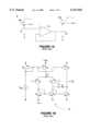
- FIG. 1Ais a block diagram 5 illustrating a conventional operational amplifier (“op-amp") 10 that may be used to drive the columns of an FED device with different voltage amplitudes.
- op-amp 10is configured as a voltage follower. More specifically, op-amp 10 is configured to receive an input voltage V, from D/A converters (not shown) and to provide the necessary current to drive the columns of the FED to the same voltage.
- Van input voltage
- D/A convertersnot shown
- One problem associated with the conventional op-amp 10is that there is a limited rate of signal change possible at the output of the op-amp 10. The maximum signal change rate is also known as the slew-rate (SR).
- SRslew-rate
- the op-amp 10will not comply. As illustrated, in response to a step function input 6a, the output of the op-amp 10 will not be able to rise instantaneously; rather, the output 6b will be the linear ramp of slope equal to SR.
- the slew rate SRis proportional to a bias current, or quiescent current, of an op-amp.
- FIG. 1Bis a common implementation of the op-amp 10 of FIG. 1A. As illustrated in FIG. 1B, op-amp 10 includes a current mirror (transistors Q5 and Q8) for providing a bias current I, which is set by reference current I REF to differential transistor pair Q1 and Q2. For the op-amp 10 illustrated in FIG. 1B, the slew rate would be given by the formula:
- C cis the capacitance of the output stage of the op-amp 10.
- One way of increasing the slew rate of the op-amp 10is to increase the reference current I REF .
- this conventional methodis simple and easy to implement, increasing the reference current I REF would significantly increase quiescent power consumption of the op-amp 10.
- quiescent conditionse.g. when voltages at the positive input and the negative input are the same
- the op-amp 10would consume a significant amount of power.
- power consumptionis a key factor in determining the commercial viability of such products because they are largely battery powered.
- the present inventionprovides for an amplifier circuit having a high slew rate and a low quiescent current.
- the amplifierincludes a voltage sensing circuit for monitoring a voltage differential between an input and an output of the amplifier circuit, and a current-boosting circuit responsive to the voltage differential for providing additional bias current to the sensing circuit.
- the slew rate of the amplifier circuit of the present inventionis increased.
- the current-boosting circuitis inactive when the input voltage and the output voltage are substantially equivalent. In this way, bias current and power dissipation are maintained at a low level during quiescent conditions.
- the current-boosting circuitis configured to be activated by both positive and negative voltage differentials.
- the current-boosting circuitcomprises two sub-circuits: a first sub-circuit for providing additional bias current to the sensing circuit responsive to a positive voltage differential; and a second sub-circuit for providing additional bias current to the sensing circuit responsive to a negative voltage differential.
- the amplifierfurther comprises a bias current limiter for limiting a maximum amount of additional bias current available to the voltage sensing circuit.
- the bias current limiteris omitted such that a maximum amount of bias current is available to drive the output at an even higher slew rate.
- the circuit for sensing a voltage differential between the input and output of the amplifiercomprises a differential pair.
- the quiescent bias currentis provided by a current mirror circuit and is proportional to a quiescent-setting current.
- Embodiments of the present inventioninclude the above and further include an FED column driver amplifier comprising: an input and an output, a sensing circuit for monitoring a voltage differential between the input and the output, a current source for providing a quiescent bias current to the sensing circuit, and a current-boosting circuit responsive to the voltage differential for providing additional bias current to the sensing circuit, wherein the current-boosting circuit is inactive when voltages at the input and the output are the same.
- an FED column driver amplifiercomprising: an input and an output, a sensing circuit for monitoring a voltage differential between the input and the output, a current source for providing a quiescent bias current to the sensing circuit, and a current-boosting circuit responsive to the voltage differential for providing additional bias current to the sensing circuit, wherein the current-boosting circuit is inactive when voltages at the input and the output are the same.
- FIG. 1Ais a block diagram illustrating a prior art operational amplifier for driving the column lines of FED devices.
- FIG. 1Bis a schematics diagram illustrating one implementation of the prior art operational amplifier of FIG. 1A.
- FIG. 2is a cross section structural view of part of a flat panel FED screen that utilizes a gated field emitter situated at the intersection of a row and a column line.
- FIG. 3is a plan view of internal portions of the flat panel FED screen of the present invention and illustrates several intersecting rows and columns of the display.
- FIG. 4illustrates a plan view of a flat panel FED screen in accordance with the present invention illustrating row and column drivers and numerous intersecting rows and columns.
- FIG. 5illustrates a schematic diagram of a column driver amplifier circuit according to one embodiment of the present invention.
- FIG. 6illustrates a schematic diagram of a column driver amplifier circuit according to another embodiment of the present invention.
- FIG. 2illustrates a multi-layer structure 75 which is a portion of an FED flat panel display.
- the multi-layer structure 75contains a field-emission backplate structure 45, also called a baseplate structure, and an electron-receiving faceplate structure 70.
- An imageis generated by faceplate structure 70.
- Backplate structure 45commonly consists of an electrically insulating backplate 65, an emitter (or cathode) electrode 60, an electrically insulating layer 55, a patterned gate electrode 50, and an electron-emissive element 40 situated in an aperture through insulating layer 55.
- One type of electron-emissive element 40is described in U.S. Pat. No. 5,608,283, issued on Mar.
- Emitter electrode 60 and electron-emissive element 40together constitute a cathode of the illustrated portion 75 of the FED flat panel display.
- Faceplate structure 70is formed with an electrically insulating faceplate 15, an anode 20, and a coating of phosphors (or phosphor deposits) 25. Electrons emitted from element 40 are received by phosphors portion 30.
- Element 40may comprise a conical molybdenum tip.
- Anode 20 of FIG. 2is maintained at a positive voltage relative to cathode 60/40.
- the anode voltageis 100-300 volts for spacing of 100-200 um between structures 45 and 70 but in other embodiments with greater spacing the anode voltage is in the kilovolt range.
- the anode voltageis also impressed on phosphors 25.
- a suitable gate voltageis applied to gate electrode 50, electrons are emitted from electron-emissive element 40 at various values of off-normal emission angle theta 42.
- the emitted electronsfollow non-linear (e.g., parabolic) trajectories indicated by lines 35 in FIG. 2 and impact on a target portion 30 of the phosphors 25.
- the phosphors struck by the emitted electronsproduce light of a selected color and represent a phosphor spot.
- a single phosphor spotcan be illuminated by thousands of emitters.
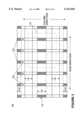
- the FED flat panel display 100is subdivided into an array of horizontally aligned rows and vertically aligned columns of pixels. A portion 100 of this array is shown in FIG. 3. The boundaries of a respective pixel 125 are indicated by dashed lines. Three separate row lines 230 are shown. Each row line 230 is a row electrode for one of the rows of pixels in the array. In one embodiment, each row line 230 is coupled to the emitter cathodes 60/40 (FIG. 2) of each emitter of the particular row associated with the electrode. A portion of one pixel row is indicated in FIG. 3 and is situated between a pair of adjacent spacer walls 135. A pixel row is comprised of all of the pixels along one row line 230.
- Each column of pixelshas three column lines 250: (1) one for red; (2) a second for green; and (3) a third for blue.
- each pixel columnincludes one of each phosphor stripes (red, green, blue), three stripes total.
- each of the column lines 250is coupled to the gate 50 (FIG. 2) of each emitter structure of the associated column.
- This structure 100is described in more detail in U.S. Pat. No. 5,477,105 issued on Dec. 19, 1995 to Curtin, et al., which is incorporated herein by reference. It should be appreciated that, in other FED designs, the column lines may be coupled to the emitter cathodes and the row lines may be coupled to the gate electrodes, and that the present invention is applicable to those FED designs as well.
- the red, green and blue phosphor stripes 25are maintained at a positive voltage relative to the voltage of the emitter-cathode 60/40.
- elements 40 in that setemit electrons which are accelerated toward a target portion 30 of the phosphors in the corresponding color.
- the excited phosphorsthen emit light.
- a screen frame refresh cycle(performed at a rate of approximately 60 Hz in one embodiment) only one row is active at a time and the column lines are energized to illuminate the one row of pixels for the on-time period.
- FIG. 4illustrates an FED flat panel display 200 in accordance with the present invention.
- Region 100as described with respect to FIG. 3, is also shown in FIG. 4.
- the FED flat panel display 200consists of n row lines (horizontal) and x column lines (vertical). For clarity, a row line is called a "row” and a column line is called a "column.” Row lines are driven by row driver circuits 220a-220c. Shown in FIG. 4 are row groups 230a, 230b and 230c. Each row group is associated with a particular row driver circuit; three row driver circuits are shown 220a-220c. In one embodiment of the present invention there are over 400 rows and approximately 5-10 row driver circuits.
- the present inventionis equally well suited to an FED flat panel display screen having any number of rows. Also shown in FIG. 4 are column groups 250a, 250b, 250c and 250d. In one embodiment of the present invention there are over 1920 columns. However, it is appreciated that the present invention is equally well suited to an FED flat panel display screen having any number of columns. A pixel requires three columns (red, green, blue), therefore, 1920 columns provides at least 640 pixel resolution horizontally.
- an enable signalis also supplied to each row driver 220a-220c in parallel over enable line 216.
- the enable line 216when the enable line 216 is low, all row drivers 220a-220c of FED screen 200 are disabled and no row is energized.
- the enable line 216is high, the row drivers 220a-220c are enabled.
- a horizontal clock signalis also supplied to each row driver 220a-220c in parallel over clock line 214.
- the horizontal clock signal or synchronization signalpulses upon each time a new row is to be energized.
- the n rows of a frameare energized, one at a time, to form a frame of data. Assuming an exemplary frame update rate of 60 Hz, all rows are updated once every 16.67 milliseconds. Assuming n rows per frame update, the horizontal clock signal pulses once every 16.67/n milliseconds. In other words a new row is energized every 16.67/n milliseconds. If n is 400, the horizontal clock signal pulses once every 41.67 microseconds.
- FIG. 4there are three columns per pixel within the FED flat panel display 200 of the present invention.
- Column lines 250acontrol one column of pixels
- column lines 250ccontrol another column line of pixels, etc.
- FIG. 4also illustrates the column drivers 240 that control the gray-scale information for each pixel.
- the column drivers 240drive amplitude modulated voltage signals over the column lines.
- the amplitude modulated voltage signals driven over the column lines 250a-250erepresent gray-scale data for a respective row of pixels.
- the column drivers 240receive gray-scale data to independently control all of the column lines 220a-220e of a pixel row of the FED flat panel display screen 200.
- column drivers 240receive column data over column data line 205 and column drivers 240 are also coupled in common to a column voltage supply line 207.
- column drivers 240are implemented on a same integrated circuit. However, it should be appreciated that column drivers 240 can be implemented on separate integrated-circuits that each drives groups of column lines.
- the column drivers 240Different voltages are applied to the column lines by the column drivers 240 to realize different gray-scale colors.
- all column linesare driven with gray-scale data (over column data line 205) and simultaneously one row is activated. This causes a row of pixels of illuminate with the proper gray-scale data. This is then repeated for another row, etc., once per pulse of the horizontal clock signal of line 214, until the entire frame is filled.
- the gray-scale data for the next pixel rowis simultaneously loaded into the column drivers 240.
- the column driversassert their voltages within the on-time window.
- the column drivers 240have an enable line.
- the column drivers 240each includes a column driver amplifier for providing necessary current to energize a respective column of the FED 200.
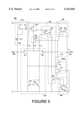
- FIG. 5is a schematic diagram illustrating an amplifier circuit 500 that can be used within the column driver 240 (FIG. 4) according to one embodiment of the present invention.
- amplifier circuit 500is configured for receiving an input voltage signal V IN from D/A converters (not shown) that convert column data from column data line 205, and for providing an output voltage signal V OUT to one of column lines 250a-d.
- amplifier circuit 500includes an input 505, an output 595, and a voltage sensing circuit 520 for monitoring a voltage differential between input 505 and output 595.
- input 505is configured for coupling to D/A converters (not shown) to receive input voltage signal V IN
- output 595is configured for coupling to one of column lines 250a-d to provide output voltage signal V OUT .
- voltage sensing circuit 520is coupled to a quiescent current source 510 to receive a quiescent current I a
- voltage sensing circuit 520is coupled to current-boosting circuits 540 and 550 to receive additional bias currents I b and I c when a voltage differential exists between input 505 and output 595.
- current-boosting circuits 540 and 550are inactive during quiescent conditions. Therefore, quiescent current and quiescent power dissipation are kept at a low level.
- amplifier circuit 500further comprises a current-steering circuit 570 coupled to voltage sensing circuit 520.
- the current-steering circuit 570is further coupled to a first output current source 560, a first current-boosting circuit 540, a second output current source 580, and a second current-boosting circuit 550.
- Output current sources 560 and 580are coupled to output 595 for providing output current.
- amplifier circuit 500further comprises a bias current limiter 530 for limiting the amount of additional bias current available to current-boosting circuits 540 and 550.
- quiescent current source 510is a current mirror circuit having a P-type MOS transistor (PMOS) 511 and a PMOS 512.
- the sources of PMOS 511 and 512are coupled to a positive supply voltage V +
- the gates of PMOS 511 and 512are coupled to a drain of PMOS 511, and to a first end of resistor 513.
- a second end of resistor 513is coupled to a negative voltage V - .
- a quiescent-setting current I QSflows from the drain of PMOS 511 across resistor 513.
- PMOS 512drives a quiescent current, I a , into voltage sensing circuit 520.
- voltage sensing circuit 520 of FIG. 5is a differential amplifier including PMOS 521 and 522, N-type MOS transistor (NMOS) 523 and NMOS 524.
- the gate of PMOS 521is coupled to input 505 to receive input voltage signal V IN
- the gate of PMOS 522is coupled to output 595 to detect output voltage signal V OUT .
- the sources of PMOS 521 and 522are coupled together and to the drain of PMOS 512 to receive quiescent current I a .
- the drain of PMOS 521is coupled to a drain of NMOS 523.
- the drain of PMOS 522is coupled to the drain of NMOS 524, and is also coupled to the gates of NMOS 523 and 524.
- the sources of NMOS 523 and 524are coupled to the negative supply voltage (e.g. V SS ).
- the drains of PMOS 521 and NMOS 523are coupled to current-steering circuit 570.
- current-steering circuit 570 of FIG. 5comprises NMOS 571 and PMOS 572.
- the gate of NMOS 571is coupled to receive a bias voltage V BIAS
- the gate of PMOS 572is coupled to the negative supply voltage V - .
- the drain of NMOS 571is coupled to first current-boosting circuit 540 and to first output current source 560.
- the source of PMOS 572is coupled to second current-boosting circuit 550 and second current source 580.
- a voltage differential between input 505 and output 595e.g.
- voltage sensing circuit 520causes current-steering circuit 570 to selectively activate a respective one of the first and second current-boosting circuits 540 and 550 to provide additional bias current.
- current-steering circuit 570selectively activates a respective one of first and second output current sources 560 and 580 to drive output 595. For example, if the voltage differential between input 505 and output 595 is positive, first output current source 560 and first current-boosting circuit 540 are activated. On the other hand, if the voltage differential is negative, second output current source 560 and second current-boosting circuit 550 are activated.
- V BIASis used for setting up a minuscule amount of continuous current flow from first current source 560 and second current source 580 to avoid "dead time.” Dead time and the mechanics of eliminating dead time are well known in the art, and are not discussed herein to avoid obscuring aspects of the present invention.
- first current-boosting circuit 540comprises a PMOS 541 having a source coupled to bias current limiter 530, a gate coupled to the drain of NMOS 571 of current-steering circuit 570, and a drain coupled to the sources of PMOS 521 and 522.
- second current-boosting circuit 540comprises an NMOS 553, and PMOS 551 and 552.
- a source of the NMOS 553is coupled to the negative supply voltage V -
- a gate of NMOS 553is coupled to a current-steering circuit 570 and second output current source 580.
- PMOS 551 and 552are coupled together in a current mirror configuration with their common sources coupled to bias current limiter 530 and their common gates coupled to the drain of PMOS 552.
- the drain of PMOS 552is also coupled to the drain of NMOS 553.
- the drain of PMOS 551is coupled to the common sources of PMOS 521 and 522 of voltage sensing circuit 520.
- first output current source 560comprises PMOS 561 and 562 configured in a current mirror configuration with their common sources coupled to receive the positive supply voltage V + , and their common gates coupled to the drain of the PMOS 561 and to current-steering circuit 570 and first current-boosting circuit 540.
- Second output current 580 of the present embodimentcomprises NMOS 581 and 582 configured in a current mirror configuration with their common sources coupled to receive the negative supply voltage V - , and with their common gates coupled to the drain of NMOS 581 and to the current-steering circuit 570 and second current-boosting circuit 550.
- the drain of NMOS 571 of FIG. 5is also coupled to the gate of PMOS 541 of first current-boosting circuit 540. Therefore, when the drain of NMOS 571 is pulled down, an additional bias current, I b , would flow into the sources of PMOS 521 and 522. In this way, when the PMOS 562 is pulling up output 595, first current-boosting circuit 540 is also pulling up on the common sources of PMOS 521 and 522 so that the bias current increases. As additional bias current is available, the slew rate of the amplifier is increased.
- the drain of PMOS 572is also coupled to the gate of NMOS 553 of second current-boosting circuit 540. Pulling up the gate of NMOS 553 will cause the common gate of PMOS 551 and 552 to be pulled down. Additionally, pulling down the gate of NMOS 553 will cause a current to flow from the drain of PMOS 552 to the drain of NMOS 553. PMOS 551 and 552 are configured as a current mirror. Therefore, an additional bias current, I C , would flow into the sources of PMOS 521 and 522. In this way, when the NMOS 582 is pulling down the output 595, second current-boosting circuit 550 is also pulling up on the common sources of the differential pair 521 and 522 so that the bias current increases. As additional bias current is available, the slew rate of the amplifier is also increased.
- bias current limiter 530comprises a PMOS transistor 531.
- the gate of PMOS 531is coupled to the gates of PMOS 511 and 512 of quiescent current source 510, and the source of PMOS 531 is coupled to the positive voltage supply V + .
- the drain of PMOS 531is coupled to first current-boosting circuit 540 and second current-boosting circuit 550.
- the maximum amount of additional bias current available to the current-boosting circuits 540 and 550is dependent upon the aspect ratios (W/L) of PMOS 531 and 512.
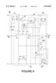
- FIG. 6illustrates a column driver amplifier circuit 600 according to an alternate embodiment of the present invention.
- column driver amplifier 600comprises input 505, output 595, voltage sensing circuit 520, a current-steering circuit 570, first output current source 560, second output current source 580, and current-boosting circuits 640 and 650.
- the column driver amplifier 600 according to the present inventionis nearly identical to the embodiment illustrated in FIG. 5. One significant difference is that, in the present embodiment, the amount of additional bias current available is not limited.
- the source of PMOS 641 of first current-boosting circuit 640is coupled to the positive supply voltage V + .
- the common source of PMOS 651 and 652 of second current-boosting circuit 650is also coupled to the positive supply voltage V + .
- Bias current-limiter 530 of FIG. 5is not present in column amplifier circuit 600. Consequently, the maximum amount of additional bias current available for current boosting circuits 640 and 650 is significantly increased, and an even higher slew rate can be achieved in the present embodiment.
Landscapes
- Engineering & Computer Science (AREA)
- Physics & Mathematics (AREA)
- Computer Hardware Design (AREA)
- General Physics & Mathematics (AREA)
- Theoretical Computer Science (AREA)
- Control Of Indicators Other Than Cathode Ray Tubes (AREA)
Abstract
Description
SR=I/C.sub.c
Claims (21)
Priority Applications (2)
| Application Number | Priority Date | Filing Date | Title |
|---|---|---|---|
| US09/162,823US6147665A (en) | 1998-09-29 | 1998-09-29 | Column driver output amplifier with low quiescent power consumption for field emission display devices |
| PCT/US1999/014110WO2000019398A1 (en) | 1998-09-29 | 1999-06-23 | Amplifier circuit for use within a column driver |
Applications Claiming Priority (1)
| Application Number | Priority Date | Filing Date | Title |
|---|---|---|---|
| US09/162,823US6147665A (en) | 1998-09-29 | 1998-09-29 | Column driver output amplifier with low quiescent power consumption for field emission display devices |
Publications (1)
| Publication Number | Publication Date |
|---|---|
| US6147665Atrue US6147665A (en) | 2000-11-14 |
Family
ID=22587271
Family Applications (1)
| Application Number | Title | Priority Date | Filing Date |
|---|---|---|---|
| US09/162,823Expired - LifetimeUS6147665A (en) | 1998-09-29 | 1998-09-29 | Column driver output amplifier with low quiescent power consumption for field emission display devices |
Country Status (2)
| Country | Link |
|---|---|
| US (1) | US6147665A (en) |
| WO (1) | WO2000019398A1 (en) |
Cited By (15)
| Publication number | Priority date | Publication date | Assignee | Title |
|---|---|---|---|---|
| US20030197473A1 (en)* | 2002-04-23 | 2003-10-23 | Shinji Kitahara | Organic EL element drive circuit and organic EL display device |
| US6646481B2 (en)* | 2001-09-28 | 2003-11-11 | Winbond Electronics Corporation | Current steering circuit for amplifier |
| US20040036670A1 (en)* | 2002-08-20 | 2004-02-26 | Samsung Electronics Co., Ltd. | Circuit and method for driving a liquid crystal display device using low power |
| US6756951B1 (en)* | 1999-08-03 | 2004-06-29 | Pioneer Corporation | Display apparatus and driving circuit of display panel |
| US20050073513A1 (en)* | 2002-12-19 | 2005-04-07 | Yoshito Date | Display driver |
| US20050140596A1 (en)* | 2003-12-30 | 2005-06-30 | Lg.Philips Lcd Co., Ltd. | Electro-luminescence display device and driving apparatus thereof |
| US20050179495A1 (en)* | 2004-02-17 | 2005-08-18 | Kuang-Feng Sung | Apparatus and method for increasing a slew rate of an operational amplifier |
| US20050248328A1 (en)* | 2004-05-04 | 2005-11-10 | Jin-Seok Yang | Driver for use in flat panel display |
| US20060119563A1 (en)* | 2001-04-27 | 2006-06-08 | Kabushiki Kaisha Toshiba | Display apparatus, digital-to-analog conversion circuit and digital-to-analog conversion method |
| US20100321360A1 (en)* | 2009-06-22 | 2010-12-23 | Renesas Electronics Corporation | Differential signal receiving circuit and display apparatus |
| US20110235689A1 (en)* | 2010-03-24 | 2011-09-29 | Kabushiki Kaisha Toshiba | Power amplifier and semiconductor integrated circuit |
| US20130016087A1 (en)* | 2011-07-15 | 2013-01-17 | Sony Corporation | Amplifier, liquid crystal displaying driving circuit and liquid crystal display apparatus |
| US10056687B2 (en) | 2016-03-04 | 2018-08-21 | Premo, S.L. | Flexible elongated inductor and elongated and flexible low-frequency antenna |
| US20220035506A1 (en)* | 2020-07-31 | 2022-02-03 | Microchip Technology Incorporated | Multi-bias mode current conveyor, configuring a multi-bias mode current conveyor, touch sensing systems including a multi-bias mode current conveyor, and related systems, methods and devices |
| US11335251B2 (en)* | 2018-11-15 | 2022-05-17 | Sapien Semiconductors Inc. | LED driving apparatus having mitigated common impedance effect |
Citations (15)
| Publication number | Priority date | Publication date | Assignee | Title |
|---|---|---|---|---|
| US4431949A (en)* | 1982-03-31 | 1984-02-14 | Tektronix, Inc. | Lateral convergence correction system |
| US5162789A (en)* | 1988-04-30 | 1992-11-10 | Nippondenso Co., Ltd. | Fluorescent indicator apparatus |
| US5469026A (en)* | 1993-11-09 | 1995-11-21 | Delco Electronics Corporation | Method and apparatus for VF tube power supply |
| US5477105A (en)* | 1992-04-10 | 1995-12-19 | Silicon Video Corporation | Structure of light-emitting device with raised black matrix for use in optical devices such as flat-panel cathode-ray tubes |
| US5541473A (en)* | 1992-04-10 | 1996-07-30 | Silicon Video Corporation | Grid addressed field emission cathode |
| US5559389A (en)* | 1993-09-08 | 1996-09-24 | Silicon Video Corporation | Electron-emitting devices having variously constituted electron-emissive elements, including cones or pedestals |
| US5564959A (en)* | 1993-09-08 | 1996-10-15 | Silicon Video Corporation | Use of charged-particle tracks in fabricating gated electron-emitting devices |
| US5578899A (en)* | 1994-11-21 | 1996-11-26 | Silicon Video Corporation | Field emission device with internal structure for aligning phosphor pixels with corresponding field emitters |
| US5608283A (en)* | 1994-06-29 | 1997-03-04 | Candescent Technologies Corporation | Electron-emitting devices utilizing electron-emissive particles which typically contain carbon |
| US5607335A (en)* | 1994-06-29 | 1997-03-04 | Silicon Video Corporation | Fabrication of electron-emitting structures using charged-particle tracks and removal of emitter material |
| US5847515A (en)* | 1996-11-01 | 1998-12-08 | Micron Technology, Inc. | Field emission display having multiple brightness display modes |
| US5867136A (en)* | 1995-10-02 | 1999-02-02 | Micron Display Technology, Inc. | Column charge coupling method and device |
| US5898415A (en)* | 1997-09-26 | 1999-04-27 | Candescent Technologies Corporation | Circuit and method for controlling the color balance of a flat panel display without reducing gray scale resolution |
| US6040809A (en)* | 1998-01-30 | 2000-03-21 | Candescent Technologies Corporation | Fed display row driver with chip-to-chip settling time matching and phase detection circuits used to prevent uneven or nonuniform brightness in display |
| US6067061A (en)* | 1998-01-30 | 2000-05-23 | Candescent Technologies Corporation | Display column driver with chip-to-chip settling time matching means |
- 1998
- 1998-09-29USUS09/162,823patent/US6147665A/ennot_activeExpired - Lifetime
- 1999
- 1999-06-23WOPCT/US1999/014110patent/WO2000019398A1/enactiveApplication Filing
Patent Citations (15)
| Publication number | Priority date | Publication date | Assignee | Title |
|---|---|---|---|---|
| US4431949A (en)* | 1982-03-31 | 1984-02-14 | Tektronix, Inc. | Lateral convergence correction system |
| US5162789A (en)* | 1988-04-30 | 1992-11-10 | Nippondenso Co., Ltd. | Fluorescent indicator apparatus |
| US5541473A (en)* | 1992-04-10 | 1996-07-30 | Silicon Video Corporation | Grid addressed field emission cathode |
| US5477105A (en)* | 1992-04-10 | 1995-12-19 | Silicon Video Corporation | Structure of light-emitting device with raised black matrix for use in optical devices such as flat-panel cathode-ray tubes |
| US5564959A (en)* | 1993-09-08 | 1996-10-15 | Silicon Video Corporation | Use of charged-particle tracks in fabricating gated electron-emitting devices |
| US5559389A (en)* | 1993-09-08 | 1996-09-24 | Silicon Video Corporation | Electron-emitting devices having variously constituted electron-emissive elements, including cones or pedestals |
| US5469026A (en)* | 1993-11-09 | 1995-11-21 | Delco Electronics Corporation | Method and apparatus for VF tube power supply |
| US5608283A (en)* | 1994-06-29 | 1997-03-04 | Candescent Technologies Corporation | Electron-emitting devices utilizing electron-emissive particles which typically contain carbon |
| US5607335A (en)* | 1994-06-29 | 1997-03-04 | Silicon Video Corporation | Fabrication of electron-emitting structures using charged-particle tracks and removal of emitter material |
| US5578899A (en)* | 1994-11-21 | 1996-11-26 | Silicon Video Corporation | Field emission device with internal structure for aligning phosphor pixels with corresponding field emitters |
| US5867136A (en)* | 1995-10-02 | 1999-02-02 | Micron Display Technology, Inc. | Column charge coupling method and device |
| US5847515A (en)* | 1996-11-01 | 1998-12-08 | Micron Technology, Inc. | Field emission display having multiple brightness display modes |
| US5898415A (en)* | 1997-09-26 | 1999-04-27 | Candescent Technologies Corporation | Circuit and method for controlling the color balance of a flat panel display without reducing gray scale resolution |
| US6040809A (en)* | 1998-01-30 | 2000-03-21 | Candescent Technologies Corporation | Fed display row driver with chip-to-chip settling time matching and phase detection circuits used to prevent uneven or nonuniform brightness in display |
| US6067061A (en)* | 1998-01-30 | 2000-05-23 | Candescent Technologies Corporation | Display column driver with chip-to-chip settling time matching means |
Non-Patent Citations (2)
| Title |
|---|
| Sendra and Smith. Microelectronic Circuits . Oxford University Press, 4th edition, 1997. pp. 839 848.* |
| Sendra and Smith. Microelectronic Circuits. Oxford University Press, 4th edition, 1997. pp. 839-848. |
Cited By (33)
| Publication number | Priority date | Publication date | Assignee | Title |
|---|---|---|---|---|
| US6756951B1 (en)* | 1999-08-03 | 2004-06-29 | Pioneer Corporation | Display apparatus and driving circuit of display panel |
| US7777739B2 (en)* | 2001-04-27 | 2010-08-17 | Kabushiki Kaisha Toshiba | Display apparatus, digital-to-analog conversion circuit and digital-to-analog conversion method |
| US20060119563A1 (en)* | 2001-04-27 | 2006-06-08 | Kabushiki Kaisha Toshiba | Display apparatus, digital-to-analog conversion circuit and digital-to-analog conversion method |
| US6646481B2 (en)* | 2001-09-28 | 2003-11-11 | Winbond Electronics Corporation | Current steering circuit for amplifier |
| US20030197473A1 (en)* | 2002-04-23 | 2003-10-23 | Shinji Kitahara | Organic EL element drive circuit and organic EL display device |
| US6946801B2 (en)* | 2002-04-23 | 2005-09-20 | Rohm Co. Ltd. | Organic EL element drive circuit and organic EL display device |
| US20040036670A1 (en)* | 2002-08-20 | 2004-02-26 | Samsung Electronics Co., Ltd. | Circuit and method for driving a liquid crystal display device using low power |
| US7317440B2 (en) | 2002-08-20 | 2008-01-08 | Samsung Electronics Co., Ltd. | Circuit and method for driving a liquid crystal display device using low power |
| US20050073513A1 (en)* | 2002-12-19 | 2005-04-07 | Yoshito Date | Display driver |
| US20050200583A1 (en)* | 2002-12-19 | 2005-09-15 | Matsushita Electric Industrial Co., Ltd. | Display driver |
| US6924601B2 (en)* | 2002-12-19 | 2005-08-02 | Matsushita Electric Industrial Co., Ltd. | Display driver |
| US7265495B2 (en) | 2002-12-19 | 2007-09-04 | Matsushita Electric Industrial Co., Ltd. | Display driver |
| US8026909B2 (en) | 2003-12-30 | 2011-09-27 | Lg Display Co., Ltd. | Electro-luminescence display device and driving apparatus thereof |
| GB2409753B (en)* | 2003-12-30 | 2006-04-19 | Lg Philips Lcd Co Ltd | Electro-luminescence display device and driving apparatus thereof |
| GB2409753A (en)* | 2003-12-30 | 2005-07-06 | Lg Philips Lcd Co Ltd | Electro-luminescence display device and driving apparatus the eof |
| US20110063280A1 (en)* | 2003-12-30 | 2011-03-17 | Dai Yun Lee | Electro-luminescence display device and driving apparatus thereof |
| US7889157B2 (en) | 2003-12-30 | 2011-02-15 | Lg Display Co., Ltd. | Electro-luminescence display device and driving apparatus thereof |
| US20050140596A1 (en)* | 2003-12-30 | 2005-06-30 | Lg.Philips Lcd Co., Ltd. | Electro-luminescence display device and driving apparatus thereof |
| US20050179495A1 (en)* | 2004-02-17 | 2005-08-18 | Kuang-Feng Sung | Apparatus and method for increasing a slew rate of an operational amplifier |
| US7173490B2 (en)* | 2004-02-17 | 2007-02-06 | Novatek Microelectronics Corp. | Apparatus and method for increasing a slew rate of an operational amplifier |
| US20060244531A1 (en)* | 2004-02-17 | 2006-11-02 | Novatek Microelectronics Corp. | Apparatus and method for increasing a slew rate of an operational amplifier |
| US7102436B2 (en)* | 2004-02-17 | 2006-09-05 | Novatek Microelectronics Corp. | Apparatus and method for increasing a slew rate of an operational amplifier |
| US8022906B2 (en)* | 2004-05-04 | 2011-09-20 | Magnachip Semiconductor, Ltd. | Driver for use in a flat panel display adapted to drive segment lines using a current |
| US20050248328A1 (en)* | 2004-05-04 | 2005-11-10 | Jin-Seok Yang | Driver for use in flat panel display |
| US20100321360A1 (en)* | 2009-06-22 | 2010-12-23 | Renesas Electronics Corporation | Differential signal receiving circuit and display apparatus |
| US20110235689A1 (en)* | 2010-03-24 | 2011-09-29 | Kabushiki Kaisha Toshiba | Power amplifier and semiconductor integrated circuit |
| US8565341B2 (en)* | 2010-03-24 | 2013-10-22 | Kabushiki Kaisha Toshiba | Power amplifier and semiconductor integrated circuit |
| US20130016087A1 (en)* | 2011-07-15 | 2013-01-17 | Sony Corporation | Amplifier, liquid crystal displaying driving circuit and liquid crystal display apparatus |
| US9520848B2 (en)* | 2011-07-15 | 2016-12-13 | Sony Corporation | Amplifier, liquid crystal displaying driving circuit and liquid crystal display apparatus |
| US10056687B2 (en) | 2016-03-04 | 2018-08-21 | Premo, S.L. | Flexible elongated inductor and elongated and flexible low-frequency antenna |
| US11335251B2 (en)* | 2018-11-15 | 2022-05-17 | Sapien Semiconductors Inc. | LED driving apparatus having mitigated common impedance effect |
| US20220035506A1 (en)* | 2020-07-31 | 2022-02-03 | Microchip Technology Incorporated | Multi-bias mode current conveyor, configuring a multi-bias mode current conveyor, touch sensing systems including a multi-bias mode current conveyor, and related systems, methods and devices |
| US11934609B2 (en)* | 2020-07-31 | 2024-03-19 | Microchip Technology Incorporated | Multi-bias mode current conveyor, configuring a multi-bias mode current conveyor, touch sensing systems including a multi-bias mode current conveyor, and related systems, methods and devices |
Also Published As
| Publication number | Publication date |
|---|---|
| WO2000019398A1 (en) | 2000-04-06 |
Similar Documents
| Publication | Publication Date | Title |
|---|---|---|
| US6147664A (en) | Controlling the brightness of an FED device using PWM on the row side and AM on the column side | |
| US6147665A (en) | Column driver output amplifier with low quiescent power consumption for field emission display devices | |
| EP1005689B1 (en) | Circuit and method for controlling the brightness of an fed device | |
| US6515641B1 (en) | Image display apparatus and method of driving image display apparatus | |
| JP3771285B2 (en) | Multiplex matrix display screen | |
| JP2001209352A (en) | Electrostatic electron emission type display device and its driving method | |
| JP2000221945A (en) | Matrix type display device | |
| US6429836B1 (en) | Circuit and method for display of interlaced and non-interlaced video information on a flat panel display apparatus | |
| EP0707301A1 (en) | Power management for a display device | |
| JPH07181916A (en) | Driving circuit of display device | |
| US5898415A (en) | Circuit and method for controlling the color balance of a flat panel display without reducing gray scale resolution | |
| US6448949B1 (en) | System and method for improving emitter life in flat panel field emission displays | |
| US6166490A (en) | Field emission display of uniform brightness independent of column trace-induced signal deterioration | |
| US5767823A (en) | Method and apparatus for gray scale modulation of a matrix display | |
| US20030058196A1 (en) | Method for reducing power consumption in field emission display devices by efficiently controlling column driver output voltage | |
| WO2000072297A9 (en) | An electronic system associated with display systems | |
| JP2000214820A (en) | Image displaying method and drive circuit for display device | |
| Chen et al. | A field-interlaced real-time gas-discharge flat-panel display with gray scale | |
| KR20060104222A (en) | Driving device of electron emission display device and driving method thereof | |
| JP2000267624A (en) | Driving circuit for matrix type display device | |
| US20050243030A1 (en) | Electron emission display and driving method thereof | |
| WO2002031803A1 (en) | Field emission display for interlaced and sequential video signals and related driving method | |
| JPH08211845A (en) | Fluorescent display device | |
| US20100321373A1 (en) | Image display apparatus and method for controlling the same | |
| WO2004017292A1 (en) | Sequentially and interlacedly scanned field emission display |
Legal Events
| Date | Code | Title | Description |
|---|---|---|---|
| AS | Assignment | Owner name:CANDESCENT TECHNOLOGIES CORPORATION, CALIFORNIA Free format text:ASSIGNMENT OF ASSIGNORS INTEREST;ASSIGNOR:FRIEDMAN, JAY;REEL/FRAME:009721/0307 Effective date:19990108 | |
| STCF | Information on status: patent grant | Free format text:PATENTED CASE | |
| AS | Assignment | Owner name:CANDESCENT INTELLECTUAL PROPERTY SERVICES, INC., C Free format text:ASSIGNMENT OF ASSIGNORS INTEREST;ASSIGNOR:CANDESCENT TECHNOLOGIES CORPORATION;REEL/FRAME:011821/0569 Effective date:20001205 | |
| FEPP | Fee payment procedure | Free format text:PAYOR NUMBER ASSIGNED (ORIGINAL EVENT CODE: ASPN); ENTITY STATUS OF PATENT OWNER: LARGE ENTITY | |
| FPAY | Fee payment | Year of fee payment:4 | |
| AS | Assignment | Owner name:CANON KABUSHIKI KAISHA, JAPAN Free format text:NUNC PRO TUNC ASSIGNMENT EFFECTIVE AS OF AUGUST 26, 2004;ASSIGNOR:CANDESCENT TECHNOLOGIES CORPORATION;REEL/FRAME:019466/0437 Effective date:20070104 | |
| AS | Assignment | Owner name:CANON KABUSHIKI KAISHA, JAPAN Free format text:NUNC PRO TUNC ASSIGNMENT;ASSIGNOR:CANDESCENT INTELLECTUAL PROPERTY SERVICES, INC.;REEL/FRAME:019580/0723 Effective date:20061226 | |
| AS | Assignment | Owner name:CANDESCENT INTELLECTUAL PROPERTY SERVICES, INC., C Free format text:CORRECTIVE ASSIGNMENT TO CORRECT THE ASSIGNEE. THE NAME OF ONE ASSIGNEE WAS INADVERTENTLY OMITTED FROM THE RECORDATION FORM COVER SHEET PREVIOUSLY RECORDED ON REEL 011821 FRAME 0569;ASSIGNOR:CANDESCENT TECHNOLOGIES CORPORATION;REEL/FRAME:019679/0375 Effective date:20001205 Owner name:CANDESCENT TECHNOLOGIES CORPORATION, CALIFORNIA Free format text:CORRECTIVE ASSIGNMENT TO CORRECT THE ASSIGNEE. THE NAME OF ONE ASSIGNEE WAS INADVERTENTLY OMITTED FROM THE RECORDATION FORM COVER SHEET PREVIOUSLY RECORDED ON REEL 011821 FRAME 0569;ASSIGNOR:CANDESCENT TECHNOLOGIES CORPORATION;REEL/FRAME:019679/0375 Effective date:20001205 | |
| FPAY | Fee payment | Year of fee payment:8 | |
| FPAY | Fee payment | Year of fee payment:12 |