US6147391A - Semiconductor hetero-interface photodetector - Google Patents
Semiconductor hetero-interface photodetectorDownload PDFInfo
- Publication number
- US6147391A US6147391AUS09/272,870US27287099AUS6147391AUS 6147391 AUS6147391 AUS 6147391AUS 27287099 AUS27287099 AUS 27287099AUS 6147391 AUS6147391 AUS 6147391A
- Authority
- US
- United States
- Prior art keywords
- semiconductor layer
- photodetector
- region
- accordance
- absorption region
- Prior art date
- Legal status (The legal status is an assumption and is not a legal conclusion. Google has not performed a legal analysis and makes no representation as to the accuracy of the status listed.)
- Expired - Lifetime
Links
Images


Classifications
- H—ELECTRICITY
- H10—SEMICONDUCTOR DEVICES; ELECTRIC SOLID-STATE DEVICES NOT OTHERWISE PROVIDED FOR
- H10F—INORGANIC SEMICONDUCTOR DEVICES SENSITIVE TO INFRARED RADIATION, LIGHT, ELECTROMAGNETIC RADIATION OF SHORTER WAVELENGTH OR CORPUSCULAR RADIATION
- H10F77/00—Constructional details of devices covered by this subclass
- H10F77/30—Coatings
- H10F77/306—Coatings for devices having potential barriers
- H—ELECTRICITY
- H10—SEMICONDUCTOR DEVICES; ELECTRIC SOLID-STATE DEVICES NOT OTHERWISE PROVIDED FOR
- H10F—INORGANIC SEMICONDUCTOR DEVICES SENSITIVE TO INFRARED RADIATION, LIGHT, ELECTROMAGNETIC RADIATION OF SHORTER WAVELENGTH OR CORPUSCULAR RADIATION
- H10F30/00—Individual radiation-sensitive semiconductor devices in which radiation controls the flow of current through the devices, e.g. photodetectors
- H10F30/20—Individual radiation-sensitive semiconductor devices in which radiation controls the flow of current through the devices, e.g. photodetectors the devices having potential barriers, e.g. phototransistors
- H10F30/21—Individual radiation-sensitive semiconductor devices in which radiation controls the flow of current through the devices, e.g. photodetectors the devices having potential barriers, e.g. phototransistors the devices being sensitive to infrared, visible or ultraviolet radiation
- H10F30/22—Individual radiation-sensitive semiconductor devices in which radiation controls the flow of current through the devices, e.g. photodetectors the devices having potential barriers, e.g. phototransistors the devices being sensitive to infrared, visible or ultraviolet radiation the devices having only one potential barrier, e.g. photodiodes
- H10F30/225—Individual radiation-sensitive semiconductor devices in which radiation controls the flow of current through the devices, e.g. photodetectors the devices having potential barriers, e.g. phototransistors the devices being sensitive to infrared, visible or ultraviolet radiation the devices having only one potential barrier, e.g. photodiodes the potential barrier working in avalanche mode, e.g. avalanche photodiodes
- H10F30/2255—Individual radiation-sensitive semiconductor devices in which radiation controls the flow of current through the devices, e.g. photodetectors the devices having potential barriers, e.g. phototransistors the devices being sensitive to infrared, visible or ultraviolet radiation the devices having only one potential barrier, e.g. photodiodes the potential barrier working in avalanche mode, e.g. avalanche photodiodes in which the active layers form heterostructures, e.g. SAM structures
Definitions
- This inventionrelates in general to a method of making a semiconductor device. More particularly, the invention relates to a process for making a heterojunction avalanche photodetector using non-lattice matched semiconductors.
- An avalanche photodetectorhas two functions: the absorption and conversion of light to an electrical signal, and the amplification of that electrical signal through avalanche multiplication. These functions can be done by a single material, such as silicon, or by two materials grown epitaxially, one for the absorption and another for the multiplication.
- the performance of an APDis based on the achievable signal processing speed and noise, which are dependent on the absorption and multiplication efficiencies. These parameters are expressed by the responsivity, the 3-dB frequency bandwidth, and the excess noise factor.
- the excess noise factor and 3-dB bandwidthare dependent on the total device thickness and the ratio between electron and hole ionization coefficients of the material used for multiplication. The larger the ratio between the electron and hole ionization coefficients, the larger the gain bandwidth product of the APD will be. Further, the larger the coefficient ratio, the less noisy the APD will be.
- the present inventiondiscloses a powerful and highly productive apparatus and method for making APDs.
- the present inventionis comprehensive and is fully integrable with present fabrication methods.
- the present inventionsolves the above-described problems by providing a method for fusing high ionization ratio materials with high efficiency absorption materials.
- One materialis used as an absorption region for converting light into an electronic signal while another material is used for the amplification region.
- the methodis easily performed and is relatively inexpensive. Further, the method provides for customization of semiconductor devices by bandwidth, since the material for the absorption region can be chosen to suit the bandwidth, without design regard for the amplification region, since lattice matching is no longer required.
- One object of the present inventionis to provide a method for making high efficiency avalanche photodetectors. Another object of the present invention is to provide a avalanche photodetector with a high ionization rate material in contact with a highly efficient absorption material.
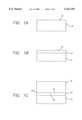
- FIGS. 1A-1Care cross-sectional views of the preparation method used for the method and product of the invention.
- FIG. 2is a flow chart describing the steps performed in the method of the invention.
- FIGS. 3A-3Lare cross-sectional views of an alternative preparation method used for the method and product of the invention.
- the present inventionprovides a method for making a heterojunction photodetector that has high efficiency and low dark current response characteristics.
- a low noise amplification regionwill have a high ratio of electron to hole ionization coefficients, which results in low noise amplification.
- Siliconis such a material, since it has a large (approximately 50:1) ratio of electron to hole ionization coefficients.
- Indium gallium arsenide (InGaAs)is a poor material for amplification, because the ratio between electron and hole ionization coefficients is approximately 1:1.
- siliconhas been fused to InP to monolithically combine InGaAs devices with silicon electronics for purposes of optoelectronic integration.
- the present inventionfuses silicon directly to InGaAs which produces detectors with performance potentials superior to existing III-V APDs in the near-infrared and superior to silicon APDs in the visible.
- Siliconis chosen as an APD multiplication region for its large electron to hole ionization coefficient ratio. These coefficients are dependent on the electric field applied to a material, but for example, at 240 kV/cm the electron to hole ratio is 50:1. In most III-V materials this ratio is much lower. For example, in InP at the same field strength the electron to hole ratio is 1:4. Comparing a silicon multiplication region to an InP multiplication region of the same width under a 240 kV/cm electric field, for a multiplication factor of 50, the 3-dB frequency bandwidth is nearly seven times higher in the silicon, and the excess noise factor is nearly five times lower. The increase in bandwidth and reduction in noise is even greater when comparing silicon with other III-V materials used as multiplication regions.
- InGaAs APDshave a high dark current (current generated under low or no-light conditions) because InGaAs is a narrow bandgap material.
- Indium Phosphide (InP)is preferred over InGaAs because InP has a larger bandgap energy than InGaAs. This larger bandgap results in lower dark currents from the avalanche region of the photodetector. InP still does not have the high ratio of electron to hole ionization coefficients, making InP a poor choice for a multiplication region.
- siliconis an ideal candidate for the amplification (also called multiplication) region, it has an indirect bandgap energy, making silicon a poor absorption material.
- the absorption coefficient of siliconis approximately 1/100 of InP or InGaAs. If a material has a small absorption coefficient, a thick absorption layer of that material is required for high efficiency, which results in a large transit time and a reduced bandwidth. Further, silicon is limited to near infrared and visible detectors because of silicon's one micron bandgap.
- the present inventionalso has a clear advantage over existing silicon APDs operating in the visible range.
- InGaAshas an absorption coefficient that is more than an order of magnitude higher than that of silicon at these wavelengths. This allows for a reduction in absorber thickness in the present invention detector compared to silicon APDs using silicon absorption regions. This reduction in thickness gives increased device speed and efficiency as well as lower device operating voltage.
- Telecommunications and far infrared applications for detectorsoperate in bandwidths that exceed the capability of silicon devices.
- InP and InGaAs devicesare able to operate in the 100 GHz range, whereas silicon is typically limited to 1 GHz. While the superiority of silicon as a multiplier is evident, silicon does not absorb in the near-infrared. Most notably, silicon does not absorb at the critical optical communications wavelengths of 1.3 and 1.55 ⁇ m.
- epitaxial growth techniqueslimited infrared APDs to infrared absorbing regions that can be lattice matched to multiplication regions, such as an InGaAs absorber and an InP multiplication region.
- Siliconwas not a feasible choice as a multiplier due to its large lattice mismatch with known infrared absorbing layers, such as InGaAs.
- the present inventionovercomes this limitation by using wafer fusion or other bonding techniques to integrate an InGaAs absorption region with silicon despite the large lattice mismatch of the two materials.
- the present inventionoutperforms the speed and noise characteristics of known combinations of III-V materials when operating in the near-infrared.
- the fusion process of the present inventionallows silicon to be fused or otherwise bonded to InGaAs or InP detectors, allowing each material to perform part of the photodetection process.
- the InP or InGaAs portionperforms the absorption and conversion process, and the electron output of the absorption region is injected into the multiplication region, where the multiplication is performed by the silicon. This results in devices that have low noise current and can operate in high frequency applications.
- FIGS. 1A-1Care cross-sectional views of the preparation method used for the method and product of the invention.
- FIG. 1Ashows a wafer 10 with top surface 12.
- the wafer 10can be made of indium gallium arsenide (In x Ga 1-x As), but can be other materials, such as indium arsenide (InAs), indium antimonide (InSb), indium gallium arsenide antimonide (In x Ga 1-x As y Sb 1-y ) mercury cadmium telluride (Hg x Cd 1-x Te), indium phosphide (InP), gallium nitride (GaN), aluminum gallium nitride (Al x Ga 1-x N), indium gallium nitride (In x Ga 1-x N), indium arsenide phosphide (InAs y P 1-y ), indium phosphide arsenide (InP y As 1-y ), indium gallium arsen
- FIG. 1Bshows a second wafer 14.
- Second wafer 14can have an epitaxial layer 16 grown on second wafer 14, but the epitaxial layer 16 is not required to practice the present invention.
- the epitaxial layer 16can be of a different material than the second wafer 14, or the epitaxial layer 16 can be of the same material as the second wafer 14.
- the second wafer 14is typically silicon, but can be other materials, such as Germanium.
- Epitaxial layer 16has a fusion surface 18, opposite to where epitaxial layer 16 contacts second wafer 14.
- FIG. 1Cshows the wafer 10 physically in contact with second wafer 14.
- the top surface 12 and the fusion surface 16are brought into close physical contact. Once this physical connection is made, and the wafer 10 and the second wafer 14 are properly aligned, heat is applied to the combination to fuse or bond the wafer 10 and the second wafer 14 together, whereby the top surface 12 and the fusion surface 18 are fused or bonded together.
- the fusion processnormally requires placing wafer 10 and second wafer 14 in an autoclave and raising the temperature to approximately 650 degrees Centigrade for silicon and indium gallium arsenide, but may be higher or lower for other materials. Other methods of bonding the wafers together may be used.
- the junction created by the physical connection between the wafer 10 and the second wafer 14is the fusion junction 20.
- wafer fusionallows the lattice geometry of the wafer 10 and the lattice geometry of the second wafer 14 to be mismatched.
- epitaxial growth of layers on the wafer 10required that the material to be grown on the top surface 12 have the same lattice constant as the material used in the wafer 10.
- lattice matchingdescribed as the distance between the atomic nuclei in a crystalline structure, is no longer required. Further, the lattice geometry, such as face centered cubic, body centered cubic, etc. does not have to match between the materials. As a consequence, materials that have desired properties for different functions within a device, such as essentially the absorption and essentially the multiplication or amplification functions of a photodetector, can now be used in their desired application, and then fused to another material that performs the remainder of the functions required by the device in a more efficient fashion.
- siliconis an excellent multiplier or amplifier, but a poor absorber in the infrared.
- InGaAsis an excellent infrared absorber, but a poor multiplier or amplifier.
- wafer fusionallows even more tailoring of devices than currently available. Devices that require higher or lower multiplication or amplification, or very narrow bandwidth absorption regions, can now be made efficiently and for lower cost. Without wafer fusion, devices are limited to either lattice matched interfaces or very thin absorbing layers that are less than the critical strain limit, reducing the possibilities for the types of materials that can be used for the different functions within each device.
- FIG. 2is a flow chart describing the steps performed in the method of the invention.
- Block 22shows providing an absorption wafer with high absorption efficiency.
- Block 22can be used to provide a wafer with a first desired property, such as high dielectric constant, low bandgap energy, direct bandgap energy, etc.
- Block 24shows providing a second wafer with a high electron/hole ionization ratio.
- Block 24can be used to provide a wafer with a second desired property, such as high conductivity, indirect band gap energy, etc.
- Block 26shows bonding or fusing the wafers together.
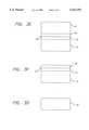
- FIGS. 3A-3Lare cross-sectional views of an alternative preparation method used for the method and product of the invention.
- FIG. 3Ashows a wafer 10 with top surface 12.
- the wafer 10is typically InP, but can be other materials.
- FIG. 3Bshows an epitaxial layer 28 grown on top surface 12 of wafer 10.
- Epitaxial layer 28is typically undoped In 0 .53 Ga 0 .47 As, but can be other materials as described in relation to FIG. 1A.
- Epitaxial layer 28is typically 1.0 to 2.0 ⁇ m thick, but can be thicker or thinner.
- FIG. 3Cshows a second wafer 14.
- Wafer 14is typically silicon, but can be other materials.
- FIG. 3Dshows epitaxial layer 16 grown on second wafer 14.
- the epitaxial layer 16is typically n-doped silicon, but can be other materials.
- Epitaxial layer 16is typically 0.5 to 2.5 ⁇ m thick, but can be thicker or thinner.
- Epitaxial layer 16has a fusion surface 18.
- FIG. 3Eshows epitaxial layer 28 physically in contact with fusion surface 18 of epitaxial layer 16. The epitaxial layer 28 is then fused to epitaxial layer 16.
- FIG. 3Fshows exposing epitaxial layer 28 by removing wafer 10.
- FIG. 3Gshows third wafer 30.
- Third wafer 30is typically InP, but can be other materials.
- FIG. 3Hshows growing epitaxial layer 32 on third wafer 30.
- Epitaxial layer 32is typically p+ doped In 0 .53 Ga 0 .47 As, but can be other materials as described in relation to FIG. 1A.
- FIG. 3Ishows epitaxial layer 32 in contact with epitaxial layer 28.
- Epitaxial layer 32is fused to epitaxial layer 28.
- the second fusion of epitaxial layer 32 to epitaxial layer 28is to minimize the diffusion of p-type dopants from the epitaxial layer 32 to the epitaxial layer 28 during the growth of the epitaxial layer 32.
- FIG. 3Jshows exposing epitaxial layer 32 by removing third wafer 30.
- FIG. 3Kshows etching epitaxial layer 32, epitaxial layer 28, and epitaxial layer 16. The etching is done to provide device isolation between individual APDs.
- FIG. 3Lshows adding contact 34 to epitaxial layer 32 and contact 36 to wafer 14.
- Contact 34 and contact 36can be the same material, or different materials.
- Contact 34is typically a gold/zinc blend, and contact 36 is typically gold. Additional materials, such as dielectric materials, can be added to provide further device isolation.
- Avalanche photodetectorswere constructed by two different methods, one using a single fusion step and another using two separate fusion steps.
- a molecular beam epitaxy (MBE) grown In 0 .53 Ga 0 .47 As/InP wafer (crystal orientation (100))was fused to an epitaxial silicon layer grown on a silicon substrate (crystal orientation (100)) with a shallow p-type ion implant at its surface.
- the epitaxial In 0 .53 Ga 0 .47 As layersconsisted of a 0.2 ⁇ m thick p+ layer and a 2.0 ⁇ m thick intrinsic layer. After the fusion step the InP substrate was removed.
- a 1.0 ⁇ m thick metal-organic chemical vapor deposition (MOCVD) grown intrinsic In 0 .53 Ga 0 .47 As layer on an InP substrate (crystal orientation (100))was fused to an intrinsic epitaxial Si layer grown on an n+ substrate (crystal orientation (100)) with a shallow p-type ion implant at its surface.
- MOCVDmetal-organic chemical vapor deposition
- the InP substratewas selectively removed leaving only the InGaAs epitaxial layer.
- a second 0.2 ⁇ m MOCVD grown p+ doped In 0 .53 Ga 0 .47 As layer on an InP substratewas then fused to the first InGaAs layer and the InP substrate subsequently removed.
- Fusion stepswere done by placing the epitaxial layers in direct contact under pressure at temperatures of 650° C. for 20 minutes in an H 2 atmosphere.
- TEM scans of the fused junction between InGaAs and Sishow covalent bonding between the materials. Also visible are edge dislocations that remain at the interface and do not thread up into the epitaxial layers.
- the two fusion step processwas used to avoid diffusion of p-type dopants from the p+ InGaAs layer into the intrinsic InGaAs layer during MOCVD growth. Some dopant diffusion is unavoidable when the intrinsic layer is grown directly over the p+ layer.
- the epitaxial layers of the finished device for both the single and two fusion step processesare as follows, starting from the topmost layer. First, a 0.2 ⁇ m thick In 0 .53 Ga 0 .47 As p+ layer with a doping level of 2 ⁇ 10 19 cm -3 is used for ohmic metal contact. The second region is a 1.0 ⁇ m or 2.0 ⁇ m thick intrinsic In 0 .53 Ga 0 .47 As layer unintentionally doped n-type used for photon absorption. This layer was fused to a Si surface implanted with a shallow 10 keV, 1.3 ⁇ 10 12 cm -2 dose of boron atoms (p-type).
- This implantbelow this implant was a 2.5 ⁇ m intrinsic epitaxial Si layer, unintentionally doped n-type with a doping level of approximately 5 ⁇ 10 14 cm -3 .
- This layerserves as the multiplication region for the detector and was grown on an n+ substrate with a doping level of 1 ⁇ 10 18 cm -3 .
- the implantation dose in the Siwas calculated to ensure that the electric field in the intrinsic Si region is higher than that in the intrinsic InGaAs region when the device is biased at operating voltages.
- electric fields of 240 kV/cm to 300 kV/cmwill be present, while the field in the InGaAs will remain below 100 kV/cm. Fields of this strength in the InGaAs layer allow for electron velocities of over 7 ⁇ 10 6 cm/sec through the region but inhibit avalanche multiplication.
- Amplification regionSilicon, unintentionally doped to 5 ⁇ 10 14 cm -3
- Absorption regionindium gallium arsenide, In 0 .53 Ga 0 .47 As
- Illumination1.3 and 1.55 ⁇ m wavelength lasers, backlighting the detector through the silicon wafer.
- the expected response of the detectoris only between 1.0 and 1.65 ⁇ m.
- Frequency response measurementswere also made on the detectors using an HP 8703a Lightwave Component Analyzer. For a 23 ⁇ m diameter device illuminated with a 1.3 ⁇ m laser, at a gain of 10, a 3-dB bandwidth of 820 MHz was measured. At a gain of 135, a 3-dB bandwidth of 600 MHz was measured yielding a gain-bandwidth product of 81 GHz. This measured gain-bandwidth product is near the highest gain-bandwidth products reported for InGaAs/InP avalanche photodetectors.
Landscapes
- Light Receiving Elements (AREA)
Abstract
Description
Claims (31)
Priority Applications (1)
| Application Number | Priority Date | Filing Date | Title |
|---|---|---|---|
| US09/272,870US6147391A (en) | 1996-05-07 | 1999-03-19 | Semiconductor hetero-interface photodetector |
Applications Claiming Priority (3)
| Application Number | Priority Date | Filing Date | Title |
|---|---|---|---|
| US64610396A | 1996-05-07 | 1996-05-07 | |
| US90713997A | 1997-08-06 | 1997-08-06 | |
| US09/272,870US6147391A (en) | 1996-05-07 | 1999-03-19 | Semiconductor hetero-interface photodetector |
Related Parent Applications (1)
| Application Number | Title | Priority Date | Filing Date |
|---|---|---|---|
| US90713997AContinuation | 1996-05-07 | 1997-08-06 |
Publications (1)
| Publication Number | Publication Date |
|---|---|
| US6147391Atrue US6147391A (en) | 2000-11-14 |
Family
ID=27094857
Family Applications (1)
| Application Number | Title | Priority Date | Filing Date |
|---|---|---|---|
| US09/272,870Expired - LifetimeUS6147391A (en) | 1996-05-07 | 1999-03-19 | Semiconductor hetero-interface photodetector |
Country Status (1)
| Country | Link |
|---|---|
| US (1) | US6147391A (en) |
Cited By (16)
| Publication number | Priority date | Publication date | Assignee | Title |
|---|---|---|---|---|
| US6362483B1 (en)* | 1998-12-29 | 2002-03-26 | The Hong Kong University Of Science & Technology | Visible-blind UV detectors |
| US6384462B1 (en) | 2000-12-06 | 2002-05-07 | Nova Crystals, Inc. | Planar hetero-interface photodetector |
| US20030067011A1 (en)* | 2001-09-06 | 2003-04-10 | Koshi Ando | Zn1-xMgxSySe1-y pin-photodiode and Zn1-xMgxSySe1-y avalanche-photodiode |
| US6583482B2 (en) | 2000-12-06 | 2003-06-24 | Alexandre Pauchard | Hetero-interface avalance photodetector |
| US20030228445A1 (en)* | 2002-06-07 | 2003-12-11 | The Procter & Gamble Company | Embossing method |
| US20040061056A1 (en)* | 2002-09-26 | 2004-04-01 | Barton Jeffrey B. | Infrared detector array with improved spectral range and method for making the same |
| US20040108530A1 (en)* | 2002-12-10 | 2004-06-10 | General Electric Company | Avalanche photodiode for use in harsh environments |
| US6794631B2 (en) | 2002-06-07 | 2004-09-21 | Corning Lasertron, Inc. | Three-terminal avalanche photodiode |
| US20050056829A1 (en)* | 2003-09-17 | 2005-03-17 | Green Michael C. | Reducing dark current of photoconductor using heterojunction that maintains high x-ray sensitivity |
| US20070170417A1 (en)* | 2006-01-20 | 2007-07-26 | The Regents Of The University Of California | III-V photonic integration on silicon |
| US20080002929A1 (en)* | 2006-06-30 | 2008-01-03 | Bowers John E | Electrically pumped semiconductor evanescent laser |
| US20080237481A1 (en)* | 2007-03-29 | 2008-10-02 | Varian Medical Systems Technologies, Inc. | Corrosion barrier layer for photoconductive X-ray imagers |
| US20090016399A1 (en)* | 2006-04-26 | 2009-01-15 | The Regents Of The University Of California | Hybrid silicon evanescent photodetectors |
| US20110284926A1 (en)* | 2010-05-18 | 2011-11-24 | Agency For Science, Technology And Research | Avalanche photodiode structure |
| US20170212221A1 (en)* | 2016-01-25 | 2017-07-27 | Canon Kabushiki Kaisha | Photoelectric conversion apparatus and information processing apparatus |
| WO2020081441A1 (en)* | 2018-10-15 | 2020-04-23 | Arizona Board Of Regents On Behalf Of Arizona State University | True hot-carrier solar cell and hot-carrier transfer |
Citations (32)
| Publication number | Priority date | Publication date | Assignee | Title |
|---|---|---|---|---|
| JPS61144816A (en)* | 1984-12-19 | 1986-07-02 | Matsushita Electric Ind Co Ltd | Semiconductor device |
| JPS61182272A (en)* | 1985-02-08 | 1986-08-14 | Toshiba Corp | Semiconductor light-receiving element |
| JPS622669A (en)* | 1985-06-28 | 1987-01-08 | Nippon Telegr & Teleph Corp <Ntt> | Solar battery and manufacture thereof |
| US4656494A (en)* | 1984-05-31 | 1987-04-07 | Fujitsu Limited | Avalanche multiplication photodiode having a buried structure |
| US4729963A (en)* | 1986-11-21 | 1988-03-08 | Bell Communications Research, Inc. | Fabrication method for modified planar semiconductor structures |
| US4761383A (en)* | 1981-09-28 | 1988-08-02 | Kokusai Denshin Denwa Kabushiki Kaisha | Method of manufacturing avalanche photo diode |
| US4839706A (en)* | 1986-08-07 | 1989-06-13 | Polaroid Corporation | Avalanche photodetector |
| US4876209A (en)* | 1988-01-06 | 1989-10-24 | U.S.C. | Method of making avalanche photodiode |
| US4914494A (en)* | 1987-07-17 | 1990-04-03 | Rca Inc. | Avalanche photodiode with central zone in active and absorptive layers |
| JPH02144974A (en)* | 1988-11-26 | 1990-06-04 | Fujitsu Ltd | Manufacturing method of semiconductor photodetector |
| JPH02189982A (en)* | 1989-01-18 | 1990-07-25 | Nec Corp | Wavelength multiple discrimination type semiconductor photodetector |
| JPH02194655A (en)* | 1989-01-24 | 1990-08-01 | Nippon Telegr & Teleph Corp <Ntt> | Waveguide-type pin photodiode for photodetection |
| US4992386A (en)* | 1988-12-14 | 1991-02-12 | Kabushiki Kaisha Toshiba | Method of manufacturing a semiconductor light detector |
| JPH0372680A (en)* | 1989-05-26 | 1991-03-27 | Mitsubishi Cable Ind Ltd | Semiconductor material, photoelectric integrated circuit element, and crystal growth method of material |
| US5008726A (en)* | 1987-11-20 | 1991-04-16 | Canon Kabushiki Kaisha | PIN junction photovoltaic element containing Zn, Se, Te, H in an amount of 1 to 4 atomic % |
| JPH03105986A (en)* | 1989-09-19 | 1991-05-02 | Fujitsu Ltd | Semiconductor photodetector |
| US5023685A (en)* | 1988-06-06 | 1991-06-11 | Bethea Clyde G | Quantum-well radiation-interactive device, and methods of radiation detection and modulation |
| JPH03184381A (en)* | 1989-12-13 | 1991-08-12 | Canon Inc | Pin type optical sensor |
| US5144637A (en)* | 1990-04-30 | 1992-09-01 | At&T Bell Laboratories | Inline diplex lightwave transceiver |
| US5252142A (en)* | 1990-11-22 | 1993-10-12 | Canon Kabushiki Kaisha | Pin junction photovoltaic element having an I-type semiconductor layer with a plurality of regions having different graded band gaps |
| US5262347A (en)* | 1991-08-14 | 1993-11-16 | Bell Communications Research, Inc. | Palladium welding of a semiconductor body |
| US5286671A (en)* | 1993-05-07 | 1994-02-15 | Kulite Semiconductor Products, Inc. | Fusion bonding technique for use in fabricating semiconductor devices |
| US5346848A (en)* | 1993-06-01 | 1994-09-13 | Motorola, Inc. | Method of bonding silicon and III-V semiconductor materials |
| US5356509A (en)* | 1992-10-16 | 1994-10-18 | Astropower, Inc. | Hetero-epitaxial growth of non-lattice matched semiconductors |
| US5386137A (en)* | 1990-04-20 | 1995-01-31 | Australian & Overseas Telecommunications Corp. Ltd. | Electro-optic device |
| US5385632A (en)* | 1993-06-25 | 1995-01-31 | At&T Laboratories | Method for manufacturing integrated semiconductor devices |
| US5389797A (en)* | 1993-02-24 | 1995-02-14 | The United States Of America As Represented By The Secretary Of The Department Of Energy | Photodetector with absorbing region having resonant periodic absorption between reflectors |
| US5393711A (en)* | 1991-10-12 | 1995-02-28 | Robert Bosch Gmbh | Process for manufacturing semiconductor components |
| US5407556A (en)* | 1992-11-11 | 1995-04-18 | Permelec Electrode Ltd. | Process of producing metallic foil by electrolysis |
| US5527732A (en)* | 1993-07-14 | 1996-06-18 | Nec Corporation | Method for fabricating semiconductor laser and photo detecting arrays for wavelength division multiplexing optical interconnections |
| US5573975A (en)* | 1994-11-04 | 1996-11-12 | Lucent Technologies Inc. | Surface-normal semiconductor optical cavity devices |
| JP3105986B2 (en) | 1992-02-10 | 2000-11-06 | 三菱レイヨン株式会社 | Production method of optically active halohydrin |
- 1999
- 1999-03-19USUS09/272,870patent/US6147391A/ennot_activeExpired - Lifetime
Patent Citations (32)
| Publication number | Priority date | Publication date | Assignee | Title |
|---|---|---|---|---|
| US4761383A (en)* | 1981-09-28 | 1988-08-02 | Kokusai Denshin Denwa Kabushiki Kaisha | Method of manufacturing avalanche photo diode |
| US4656494A (en)* | 1984-05-31 | 1987-04-07 | Fujitsu Limited | Avalanche multiplication photodiode having a buried structure |
| JPS61144816A (en)* | 1984-12-19 | 1986-07-02 | Matsushita Electric Ind Co Ltd | Semiconductor device |
| JPS61182272A (en)* | 1985-02-08 | 1986-08-14 | Toshiba Corp | Semiconductor light-receiving element |
| JPS622669A (en)* | 1985-06-28 | 1987-01-08 | Nippon Telegr & Teleph Corp <Ntt> | Solar battery and manufacture thereof |
| US4839706A (en)* | 1986-08-07 | 1989-06-13 | Polaroid Corporation | Avalanche photodetector |
| US4729963A (en)* | 1986-11-21 | 1988-03-08 | Bell Communications Research, Inc. | Fabrication method for modified planar semiconductor structures |
| US4914494A (en)* | 1987-07-17 | 1990-04-03 | Rca Inc. | Avalanche photodiode with central zone in active and absorptive layers |
| US5008726A (en)* | 1987-11-20 | 1991-04-16 | Canon Kabushiki Kaisha | PIN junction photovoltaic element containing Zn, Se, Te, H in an amount of 1 to 4 atomic % |
| US4876209A (en)* | 1988-01-06 | 1989-10-24 | U.S.C. | Method of making avalanche photodiode |
| US5023685A (en)* | 1988-06-06 | 1991-06-11 | Bethea Clyde G | Quantum-well radiation-interactive device, and methods of radiation detection and modulation |
| JPH02144974A (en)* | 1988-11-26 | 1990-06-04 | Fujitsu Ltd | Manufacturing method of semiconductor photodetector |
| US4992386A (en)* | 1988-12-14 | 1991-02-12 | Kabushiki Kaisha Toshiba | Method of manufacturing a semiconductor light detector |
| JPH02189982A (en)* | 1989-01-18 | 1990-07-25 | Nec Corp | Wavelength multiple discrimination type semiconductor photodetector |
| JPH02194655A (en)* | 1989-01-24 | 1990-08-01 | Nippon Telegr & Teleph Corp <Ntt> | Waveguide-type pin photodiode for photodetection |
| JPH0372680A (en)* | 1989-05-26 | 1991-03-27 | Mitsubishi Cable Ind Ltd | Semiconductor material, photoelectric integrated circuit element, and crystal growth method of material |
| JPH03105986A (en)* | 1989-09-19 | 1991-05-02 | Fujitsu Ltd | Semiconductor photodetector |
| JPH03184381A (en)* | 1989-12-13 | 1991-08-12 | Canon Inc | Pin type optical sensor |
| US5386137A (en)* | 1990-04-20 | 1995-01-31 | Australian & Overseas Telecommunications Corp. Ltd. | Electro-optic device |
| US5144637A (en)* | 1990-04-30 | 1992-09-01 | At&T Bell Laboratories | Inline diplex lightwave transceiver |
| US5252142A (en)* | 1990-11-22 | 1993-10-12 | Canon Kabushiki Kaisha | Pin junction photovoltaic element having an I-type semiconductor layer with a plurality of regions having different graded band gaps |
| US5262347A (en)* | 1991-08-14 | 1993-11-16 | Bell Communications Research, Inc. | Palladium welding of a semiconductor body |
| US5393711A (en)* | 1991-10-12 | 1995-02-28 | Robert Bosch Gmbh | Process for manufacturing semiconductor components |
| JP3105986B2 (en) | 1992-02-10 | 2000-11-06 | 三菱レイヨン株式会社 | Production method of optically active halohydrin |
| US5356509A (en)* | 1992-10-16 | 1994-10-18 | Astropower, Inc. | Hetero-epitaxial growth of non-lattice matched semiconductors |
| US5407556A (en)* | 1992-11-11 | 1995-04-18 | Permelec Electrode Ltd. | Process of producing metallic foil by electrolysis |
| US5389797A (en)* | 1993-02-24 | 1995-02-14 | The United States Of America As Represented By The Secretary Of The Department Of Energy | Photodetector with absorbing region having resonant periodic absorption between reflectors |
| US5286671A (en)* | 1993-05-07 | 1994-02-15 | Kulite Semiconductor Products, Inc. | Fusion bonding technique for use in fabricating semiconductor devices |
| US5346848A (en)* | 1993-06-01 | 1994-09-13 | Motorola, Inc. | Method of bonding silicon and III-V semiconductor materials |
| US5385632A (en)* | 1993-06-25 | 1995-01-31 | At&T Laboratories | Method for manufacturing integrated semiconductor devices |
| US5527732A (en)* | 1993-07-14 | 1996-06-18 | Nec Corporation | Method for fabricating semiconductor laser and photo detecting arrays for wavelength division multiplexing optical interconnections |
| US5573975A (en)* | 1994-11-04 | 1996-11-12 | Lucent Technologies Inc. | Surface-normal semiconductor optical cavity devices |
Non-Patent Citations (26)
| Title |
|---|
| Ackley, et al., "In 0.53Gao.47As/InP Floating Guard Ring Avalanche Photodiodes Fabricated by Double Diffusion", IEEE Photonics Technology Letters, vol. 2, No. 8, 1990. |
| Ackley, et al., In 0.53Gao.47As/InP Floating Guard Ring Avalanche Photodiodes Fabricated by Double Diffusion , IEEE Photonics Technology Letters, vol. 2, No. 8, 1990.* |
| Campbell, "Heterojunction Photodetectors for Optical Communications", Heterostructures and Quantum Devices, pp. 243-271, Academic Press, New York (1994). |
| Campbell, Heterojunction Photodetectors for Optical Communications , Heterostructures and Quantum Devices, pp. 243 271, Academic Press, New York (1994).* |
| Capasso, "Physics of Avalanche Photodetectors", Semiconductors and Semimetals, vol. 22, pp. 1-172, Academic Press, New York (1985). |
| Capasso, Physics of Avalanche Photodetectors , Semiconductors and Semimetals, vol. 22, pp. 1 172, Academic Press, New York (1985).* |
| Cook, et al., "Electron and hole impact ionization coefficients in InP determined by photomultiplication measurements", Appl. Phys. Lett., 40, No. 7, pp. 589-591 (1982). |
| Cook, et al., Electron and hole impact ionization coefficients in InP determined by photomultiplication measurements , Appl. Phys. Lett., 40, No. 7, pp. 589 591 (1982).* |
| Emmons, "Avalanche-Photodiode Frequency Response", Journal of Applied Physics, 38, No. 9, pp. 3705-3714. |
| Emmons, Avalanche Photodiode Frequency Response , Journal of Applied Physics, 38, No. 9, pp. 3705 3714.* |
| Grant, "Electron and Hole Ionization Rates in Epitaxial Silicon at High Electric Fields", Solid-State Electronics, 16, pp. 1189-1203 (1973). |
| Grant, Electron and Hole Ionization Rates in Epitaxial Silicon at High Electric Fields , Solid State Electronics, 16, pp. 1189 1203 (1973).* |
| Law, et al., "Interband Scattering Effects on Secondary Ionization Coefficients in GaAs", Solid-State Electronics, 21, pp. 331-340 (1978). |
| Law, et al., Interband Scattering Effects on Secondary Ionization Coefficients in GaAs , Solid State Electronics, 21, pp. 331 340 (1978).* |
| Littlejohn, et al., High field transport in InaAs and related heterostructures, Properties of Latticue Matched and Strained Indium Gallium Arsenide, pp. 107 116, INSPEC, London, (1993).* |
| Littlejohn, et al., High-field transport in InaAs and related heterostructures, Properties of Latticue-Matched and Strained Indium Gallium Arsenide, pp. 107-116, INSPEC, London, (1993). |
| Lo, et al., "Semiconductor lasers on Si substrates using the technology of bonding by atomic rearrangement" Appl. Phys. Lett., 62, pp. 1038-1040 (1993). |
| Lo, et al., Semiconductor lasers on Si substrates using the technology of bonding by atomic rearrangement Appl. Phys. Lett., 62, pp. 1038 1040 (1993).* |
| Mori, et al., "High-quality in InGaSa/InP multi-quantum-well structures on Si fabricated by direct bonding", Electron. Lett., 30, pp. 1008-1009. |
| Mori, et al., High quality in InGaSa/InP multi quantum well structures on Si fabricated by direct bonding , Electron. Lett., 30, pp. 1008 1009.* |
| Pearsall, Impact ionization rates for electrons and holes in Ga0.47In0.53As, Applied Physics Letters, 36, pp. 218 220, (1980).* |
| Pearsall, Impact ionization rates for electrons and holes in Ga0.47In0.53As, Applied Physics Letters, 36, pp. 218-220, (1980). |
| Smith, et al., "Sensitivity of Avalanche Photodetector Receivers for Long-Wavelength Optical Communications," The Bell System Technical Journal, 61, No. 10, pp. 2929-2946 (1982). |
| Smith, et al., Sensitivity of Avalanche Photodetector Receivers for Long Wavelength Optical Communications, The Bell System Technical Journal, 61, No. 10, pp. 2929 2946 (1982).* |
| Webb, et al., "Properties of Avalanche Photodiodes", RCA Review, vol. 35, pp. 234-279, (1974). |
| Webb, et al., Properties of Avalanche Photodiodes , RCA Review, vol. 35, pp. 234 279, (1974).* |
Cited By (30)
| Publication number | Priority date | Publication date | Assignee | Title |
|---|---|---|---|---|
| US6362483B1 (en)* | 1998-12-29 | 2002-03-26 | The Hong Kong University Of Science & Technology | Visible-blind UV detectors |
| US6583482B2 (en) | 2000-12-06 | 2003-06-24 | Alexandre Pauchard | Hetero-interface avalance photodetector |
| US6384462B1 (en) | 2000-12-06 | 2002-05-07 | Nova Crystals, Inc. | Planar hetero-interface photodetector |
| US6724018B2 (en)* | 2001-09-06 | 2004-04-20 | Sumitomo Electric Industries, Ltd. | Zn1-xMgxSySe1-y pin-photodiode and Zn1-xMgxSySe1-y avalanche-photodiode |
| US20030067011A1 (en)* | 2001-09-06 | 2003-04-10 | Koshi Ando | Zn1-xMgxSySe1-y pin-photodiode and Zn1-xMgxSySe1-y avalanche-photodiode |
| US20030228445A1 (en)* | 2002-06-07 | 2003-12-11 | The Procter & Gamble Company | Embossing method |
| US6794631B2 (en) | 2002-06-07 | 2004-09-21 | Corning Lasertron, Inc. | Three-terminal avalanche photodiode |
| US20040061056A1 (en)* | 2002-09-26 | 2004-04-01 | Barton Jeffrey B. | Infrared detector array with improved spectral range and method for making the same |
| US6852976B2 (en)* | 2002-09-26 | 2005-02-08 | Indigo Systems Corporation | Infrared detector array with improved spectral range and method for making the same |
| US20040108530A1 (en)* | 2002-12-10 | 2004-06-10 | General Electric Company | Avalanche photodiode for use in harsh environments |
| US6838741B2 (en) | 2002-12-10 | 2005-01-04 | General Electtric Company | Avalanche photodiode for use in harsh environments |
| US20050098844A1 (en)* | 2002-12-10 | 2005-05-12 | Sandvik Peter M. | Detection system including avalanche photodiode for use in harsh environments |
| US7002156B2 (en) | 2002-12-10 | 2006-02-21 | General Electric Company | Detection system including avalanche photodiode for use in harsh environments |
| US20050056829A1 (en)* | 2003-09-17 | 2005-03-17 | Green Michael C. | Reducing dark current of photoconductor using heterojunction that maintains high x-ray sensitivity |
| US20070170417A1 (en)* | 2006-01-20 | 2007-07-26 | The Regents Of The University Of California | III-V photonic integration on silicon |
| US8994004B2 (en) | 2006-01-20 | 2015-03-31 | The Regent Of The University Of California | Hybrid silicon optoelectronic device and method of formation |
| US9910220B2 (en) | 2006-01-20 | 2018-03-06 | The Regents Of The University Of California | III-V photonic integration on silicon |
| US9097848B2 (en) | 2006-01-20 | 2015-08-04 | The Regents Of The University Of California | III-V photonic integration on silicon |
| US8110823B2 (en) | 2006-01-20 | 2012-02-07 | The Regents Of The University Of California | III-V photonic integration on silicon |
| US8937296B2 (en) | 2006-01-20 | 2015-01-20 | The Regents Of The University Of California | III-V photonic integration on silicon |
| US20090016399A1 (en)* | 2006-04-26 | 2009-01-15 | The Regents Of The University Of California | Hybrid silicon evanescent photodetectors |
| US8106379B2 (en) | 2006-04-26 | 2012-01-31 | The Regents Of The University Of California | Hybrid silicon evanescent photodetectors |
| US20080002929A1 (en)* | 2006-06-30 | 2008-01-03 | Bowers John E | Electrically pumped semiconductor evanescent laser |
| US8767792B2 (en) | 2006-06-30 | 2014-07-01 | Intel Corporation | Method for electrically pumped semiconductor evanescent laser |
| US8232531B2 (en) | 2007-03-29 | 2012-07-31 | Varian Medical Systems, Inc. | Corrosion barrier layer for photoconductive X-ray imagers |
| US20080237481A1 (en)* | 2007-03-29 | 2008-10-02 | Varian Medical Systems Technologies, Inc. | Corrosion barrier layer for photoconductive X-ray imagers |
| US20110284926A1 (en)* | 2010-05-18 | 2011-11-24 | Agency For Science, Technology And Research | Avalanche photodiode structure |
| US20170212221A1 (en)* | 2016-01-25 | 2017-07-27 | Canon Kabushiki Kaisha | Photoelectric conversion apparatus and information processing apparatus |
| WO2020081441A1 (en)* | 2018-10-15 | 2020-04-23 | Arizona Board Of Regents On Behalf Of Arizona State University | True hot-carrier solar cell and hot-carrier transfer |
| US11749770B2 (en) | 2018-10-15 | 2023-09-05 | Arizona Board Of Regents On Behalf Of Arizona State University | True hot-carrier solar cell and hot-carrier transfer |
Similar Documents
| Publication | Publication Date | Title |
|---|---|---|
| US6465803B1 (en) | Semiconductor hetero-interface photodetector | |
| US6384462B1 (en) | Planar hetero-interface photodetector | |
| US6147391A (en) | Semiconductor hetero-interface photodetector | |
| US5525828A (en) | High speed silicon-based lateral junction photodetectors having recessed electrodes and thick oxide to reduce fringing fields | |
| US7795064B2 (en) | Front-illuminated avalanche photodiode | |
| US6326654B1 (en) | Hybrid ultraviolet detector | |
| Lee | Photodetectors | |
| Susa et al. | Characteristics in InGaAs/InP avalanche photodiodes with separated absorption and multiplication regions | |
| US4390889A (en) | Photodiode having an InGaAs layer with an adjacent InGaAsP p-n junction | |
| CN120614882A (en) | An avalanche photodiode | |
| EP0181391B1 (en) | Back-illuminated photodiode with wide bandgap cap layer | |
| US6583482B2 (en) | Hetero-interface avalance photodetector | |
| Burroughes et al. | 1.3 mu m InGaAs MSM photodetector with abrupt InGaAs/AlInAs interface | |
| Jang et al. | Long-wavelength In/sub 0.53/Ga/sub 0.47/As metamorphic pin photodiodes on GaAs substrates | |
| Sidhu et al. | 2.4 µm cutoff wavelength avalanche photodiode on InP substrate | |
| US7009224B2 (en) | Metamorphic long wavelength high-speed photodiode | |
| Nie et al. | Quantum-dot resonant-cavity separate absorption, charge, and multiplication avalanche photodiode operating at 1.06 μm | |
| Olsen et al. | Current status of InGaAs detector arrays for 1-3 um | |
| CA1149497A (en) | Iii-v quaternary alloy photodiode | |
| JPH11330536A (en) | Semiconductor light receiving element | |
| Jang et al. | The impact of a large bandgap drift region in long-wavelength metamorphic photodiodes | |
| Sutter et al. | Thin film photodetectors grown epitaxially on silicon | |
| Torres-J et al. | A planar amorphous Si/sub 1-x/Ge x Separated-Absorption-Multiplication avalanche photo diode | |
| JPS59163878A (en) | Semiconductor photodetector | |
| Hughes | III-V Compound semiconductor superlattices for infrared photodetector applications |
Legal Events
| Date | Code | Title | Description |
|---|---|---|---|
| STCF | Information on status: patent grant | Free format text:PATENTED CASE | |
| FEPP | Fee payment procedure | Free format text:PAYOR NUMBER ASSIGNED (ORIGINAL EVENT CODE: ASPN); ENTITY STATUS OF PATENT OWNER: SMALL ENTITY | |
| FPAY | Fee payment | Year of fee payment:4 | |
| FPAY | Fee payment | Year of fee payment:8 | |
| FEPP | Fee payment procedure | Free format text:PAT HOLDER CLAIMS SMALL ENTITY STATUS, ENTITY STATUS SET TO SMALL (ORIGINAL EVENT CODE: LTOS); ENTITY STATUS OF PATENT OWNER: SMALL ENTITY | |
| FPAY | Fee payment | Year of fee payment:12 | |
| AS | Assignment | Owner name:DEUTSCHE BANK AG NEW YORK BRANCH, NEW YORK Free format text:SECURITY INTEREST;ASSIGNOR:CIENA CORPORATION;REEL/FRAME:033329/0417 Effective date:20140715 | |
| AS | Assignment | Owner name:BANK OF AMERICA, N.A., AS ADMINISTRATIVE AGENT, NO Free format text:PATENT SECURITY AGREEMENT;ASSIGNOR:CIENA CORPORATION;REEL/FRAME:033347/0260 Effective date:20140715 | |
| AS | Assignment | Owner name:CIENA CORPORATION, MARYLAND Free format text:RELEASE BY SECURED PARTY;ASSIGNOR:DEUTSCHE BANK AG NEW YORK BRANCH;REEL/FRAME:050938/0389 Effective date:20191028 | |
| AS | Assignment | Owner name:BANK OF AMERICA, N.A., AS COLLATERAL AGENT, ILLINO Free format text:PATENT SECURITY AGREEMENT;ASSIGNOR:CIENA CORPORATION;REEL/FRAME:050969/0001 Effective date:20191028 | |
| AS | Assignment | Owner name:CIENA CORPORATION, MARYLAND Free format text:RELEASE BY SECURED PARTY;ASSIGNOR:BANK OF AMERICA, N.A.;REEL/FRAME:065630/0232 Effective date:20231024 |