US6146963A - Methods for forming ferroelectric capacitors having a bottom electrode with decreased leakage current - Google Patents
Methods for forming ferroelectric capacitors having a bottom electrode with decreased leakage currentDownload PDFInfo
- Publication number
- US6146963A US6146963AUS09/221,620US22162098AUS6146963AUS 6146963 AUS6146963 AUS 6146963AUS 22162098 AUS22162098 AUS 22162098AUS 6146963 AUS6146963 AUS 6146963A
- Authority
- US
- United States
- Prior art keywords
- film
- forming
- strontium
- ruthenium
- electrode
- Prior art date
- Legal status (The legal status is an assumption and is not a legal conclusion. Google has not performed a legal analysis and makes no representation as to the accuracy of the status listed.)
- Expired - Lifetime
Links
Images
Classifications
- H—ELECTRICITY
- H10—SEMICONDUCTOR DEVICES; ELECTRIC SOLID-STATE DEVICES NOT OTHERWISE PROVIDED FOR
- H10B—ELECTRONIC MEMORY DEVICES
- H10B12/00—Dynamic random access memory [DRAM] devices
- H—ELECTRICITY
- H10—SEMICONDUCTOR DEVICES; ELECTRIC SOLID-STATE DEVICES NOT OTHERWISE PROVIDED FOR
- H10D—INORGANIC ELECTRIC SEMICONDUCTOR DEVICES
- H10D1/00—Resistors, capacitors or inductors
- H10D1/60—Capacitors
- H10D1/68—Capacitors having no potential barriers
- H10D1/692—Electrodes
- H10D1/696—Electrodes comprising multiple layers, e.g. comprising a barrier layer and a metal layer
- H—ELECTRICITY
- H10—SEMICONDUCTOR DEVICES; ELECTRIC SOLID-STATE DEVICES NOT OTHERWISE PROVIDED FOR
- H10D—INORGANIC ELECTRIC SEMICONDUCTOR DEVICES
- H10D1/00—Resistors, capacitors or inductors
- H10D1/60—Capacitors
- H10D1/68—Capacitors having no potential barriers
- H10D1/682—Capacitors having no potential barriers having dielectrics comprising perovskite structures
- H10D1/684—Capacitors having no potential barriers having dielectrics comprising perovskite structures the dielectrics comprising multiple layers, e.g. comprising buffer layers, seed layers or gradient layers
Definitions
- the present inventionrelates to methods for fabricating semiconductor devices; and, particularly, to methods for forming ferroelectric capacitors which have a film of ruthenium dioxide (RuO 2 ) as a bottom electrode and is enhanced in characteristics about leakage current.
- RuO 2ruthenium dioxide
- semiconductor memory elements having non-volatile characteristicsuse remanent polarization of ferroelectric materials which have two stable state of remanent polarization and dielectric constant of which is hundreds to thousands at room temperature in order to store information for a long time.
- a polycrystalline ferroelectric thin film of strontium bismuth tantalatehereinafter, referred to as SBT is chiefly used as the ferroelectric film.
- the non-volatile memory element having the ferroelectric thin filmuses the principle that if it is controlled to direct its polarization according to electric field and to input a signal, the digital signal 1 (high) or 0 (low) is stored in it by the direction of the remaining remanent polarization when the electric field is removed.
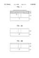
- FIG. 1shows the ferroelectric capacitor formed according to the prior art. Referring to this, described is the method for forming the ferroelectric capacitor in the prior art and its drawbacks.
- a transistor(not shown) is formed over a silicon substrate 11
- an insulating filmfor example, a SiO 2 film 12 is formed to insulate the transistor.
- the SiO 2 film 12is then selectively etched to form a contact hole followed by burying polysilicon in the contact hole to form a polysilicon plug 13 connected to the source or drain region of the transistor.
- Films of Ti/TiN 14are then formed as diffusion barriers and patterned, followed by forming a lower electrode 15, a SBT ferroelectric thin film 16, and an upper electrode 17, in turn, over the films of Ti/TiN 14 to form a capacitor.
- a film of ruthenium dioxideis generally used as a bottom electrode 15 of the SBT ferroelectric thin film 16.
- the ruthenium dioxide filmshows better characteristics in the fatigue or loss of the polarization switching of the ferroelectric thin film due to electric cycling, compared with the other materials used as electrodes.
- an object of the present inventionto provide methods for forming ferroelectric capacitors which can prevent decreasing characteristics about leakage current at the time of post-thermal treatment of the SBT ferroelectric thin film among the capacitor formation processes and, thus, minimize the generation of leakage current.
- a method for forming a ferroelectric capacitorwhich comprises the steps of: forming a first electrode of ruthenium dioxide over a lower layer including a conductive plug, the electrode being connected to the conductive plug; forming a film of strontium on the first electrode of ruthenium dioxide; forming a film of strontium ruthenium oxide by performing thermal treatment of the strontium film under oxygen atmosphere in order to prevent the diffusion of oxygen to the electrode of ruthenium dioxide; forming a thin film of crystallized ferroelectric material on the film of strontium ruthenium oxide; forming a second film of ruthenium dioxide on the ferroelectric film.
- FIG. 1shows the capacitor formed according to the prior art.
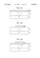
- FIGS. 2a through 2idepict, schematically, various steps in the forming of the ferroelectric capacitor according to a preferred embodiment of the invention.
- a transistor(not shown) is formed over a silicon substrate 21, an insulating film, i.e., a SiO 2 film 22 is formed to insulate the transistor, and the SiO 2 film 22 is then selectively etched to form a contact hole. At this point, the source or drain region of the transistor is exposed.
- Polysiliconis deposited to a thickness of about 500 to 3000 ⁇ by chemical vapor deposition so as to be buried in the contact hole and a polysilicon plug 23 is formed by entirely etching the polysilicon film and remaining the polysilicon only in the contact hole. The polysilicon plug 23 is connected to the source or drain region of the transistor.
- a film of Ti 24is deposited as a diffusion barrier to a thickness of about 100 to 1000 ⁇ .
- a film of TiN 25is then formed on the Ti film to a thickness of about 200 to 2000 ⁇ .
- the Ti film 24 and TiN film 25are formed as metal diffusion barriers between the polysilicon plug 23 and a bottom metal electrode which will be formed later as described below.
- the Ti film 24 and the TiN film 25are patterned and etched by photoresist and dry etching processes as known in the art to remain them only in the certain region overlapped with the polysilicon plug 23.
- a film of ruthenium 26is deposited as an oxygen diffusion barrier over the entire structure to a thickness of about 100 to 1000 ⁇ .
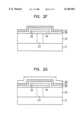
- a film of strontium 28is coated on the film of ruthenium dioxide 27 to a thickness of about 100 to 500 ⁇ by spinning at 1500 to 3500 rpm for 10 to 30 seconds. This is different from the prior method in which a thin film of ferroelectric material is formed on the film of ruthenium dioxide at this point.
- the film of strontium 28 coated on the film of ruthenium dioxide 27is changed to a strontium ruthenium oxide (SrRuO 3 ) 29 by performing thermal treatment at a temperature of 400 to 800° C. under oxygen atmosphere.
- the film of strontium ruthenium oxide 29is an oxygen diffusion barrier and will later prevent the film of ruthenium dioxide 27 from being oxidized at the time of thermal process of a ferroelectric film (described as below) at high temperature under oxygen atmosphere. This is suggested by the invention.
- the inventioncan sufficiently overcome the prior problems about leakage current in capacitors using the film of ruthenium dioxide as a bottom electrode 27 by forming the film of strontium ruthenium oxide 29 as an oxygen diffusion barrier.
- a thin film of SBT ferroelectric material 30is coated on the strontium ruthenium oxide 29 to a thickness of about 1000 to 5000 ⁇ by spinning at 1500 to 3500 rpm for 10 to 30 seconds. It is then crystallized by performing thermal treatment at a high temperature of about 600 to 900° C. under oxygen atmosphere for 30 to 90 minutes.
- the process conditionssuch as temperature and time can be reduced and the yield of the device can be enhanced.
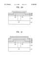
- a film of ruthenium dioxide 31is formed as an upper electrode to a thickness of about 500 to 2000 ⁇ on the crystallized SBT ferroelectric film having high dielectric constant, thus to complete the formation of a capacitor.
- the metal diffusion barrier filmmay be formed using films of tantalum/tantalum nitride instead of the films of Ti/TiN.
- the ruthenium film 26may be also directly deposited on the polysilicon plug 23 without the formation of the metal diffusion barrier films.
Landscapes
- Semiconductor Memories (AREA)
Abstract
Description
Claims (9)
Applications Claiming Priority (2)
| Application Number | Priority Date | Filing Date | Title |
|---|---|---|---|
| KR1019970075086AKR100458084B1 (en) | 1997-12-27 | 1997-12-27 | Ferroelectric Capacitor Formation Method with Lower Electrode with Reduced Leakage Current |
| KR97-75086 | 1997-12-27 |
Publications (1)
| Publication Number | Publication Date |
|---|---|
| US6146963Atrue US6146963A (en) | 2000-11-14 |
Family
ID=19528934
Family Applications (1)
| Application Number | Title | Priority Date | Filing Date |
|---|---|---|---|
| US09/221,620Expired - LifetimeUS6146963A (en) | 1997-12-27 | 1998-12-28 | Methods for forming ferroelectric capacitors having a bottom electrode with decreased leakage current |
Country Status (3)
| Country | Link |
|---|---|
| US (1) | US6146963A (en) |
| KR (1) | KR100458084B1 (en) |
| TW (1) | TW400639B (en) |
Cited By (8)
| Publication number | Priority date | Publication date | Assignee | Title |
|---|---|---|---|---|
| US20030186501A1 (en)* | 2002-03-26 | 2003-10-02 | Rueger Neal R. | Methods of forming semiconductor constructions |
| US6645779B2 (en)* | 2001-03-28 | 2003-11-11 | Hynix Semiconductor Inc. | FeRAM (ferroelectric random access memory) and method for forming the same |
| US6674633B2 (en)* | 2001-02-28 | 2004-01-06 | Fujitsu Limited | Process for producing a strontium ruthenium oxide protective layer on a top electrode |
| DE10255841A1 (en)* | 2002-11-29 | 2004-06-17 | Infineon Technologies Ag | Process for structuring ruthenium or ruthenium (IV) oxide layers used for a trench capacitor comprises depositing ruthenium or ruthenium (IV) oxide on sections of a substrate, depositing a covering layer, and further processing |
| US7015531B2 (en)* | 2001-03-07 | 2006-03-21 | Hynix Semiconductor Inc. | FeRAM having bottom electrode connected to storage node and method for forming the same |
| US20100020509A1 (en)* | 2006-03-31 | 2010-01-28 | University Of Florida Research Foundation, Inc | Integrated Power Passives |
| US8518793B2 (en) | 2011-10-21 | 2013-08-27 | Imec | Oxygen diffusion barrier comprising Ru |
| US20170298520A1 (en)* | 2016-04-19 | 2017-10-19 | Ricoh Company, Ltd. | Ferroelectric element and method of manufacturing ferroelectric element |
Families Citing this family (2)
| Publication number | Priority date | Publication date | Assignee | Title |
|---|---|---|---|---|
| KR100353809B1 (en)* | 1999-12-28 | 2002-09-26 | 주식회사 하이닉스반도체 | Method for manufacturing ferroelectric capacitor |
| US6475854B2 (en)* | 1999-12-30 | 2002-11-05 | Applied Materials, Inc. | Method of forming metal electrodes |
Citations (20)
| Publication number | Priority date | Publication date | Assignee | Title |
|---|---|---|---|---|
| US5254217A (en)* | 1992-07-27 | 1993-10-19 | Motorola, Inc. | Method for fabricating a semiconductor device having a conductive metal oxide |
| US5358889A (en)* | 1993-04-29 | 1994-10-25 | Northern Telecom Limited | Formation of ruthenium oxide for integrated circuits |
| JPH0750285A (en)* | 1993-06-10 | 1995-02-21 | Sharp Corp | Method for reactive ion etching of lead zirconate titanate and ruthenium oxide thin films and semiconductor device manufactured using the same |
| US5407855A (en)* | 1993-06-07 | 1995-04-18 | Motorola, Inc. | Process for forming a semiconductor device having a reducing/oxidizing conductive material |
| US5440173A (en)* | 1993-09-17 | 1995-08-08 | Radiant Technologies | High-temperature electrical contact for making contact to ceramic materials and improved circuit element using the same |
| US5466629A (en)* | 1992-07-23 | 1995-11-14 | Symetrix Corporation | Process for fabricating ferroelectric integrated circuit |
| US5491102A (en)* | 1992-04-13 | 1996-02-13 | Ceram Incorporated | Method of forming multilayered electrodes for ferroelectric devices consisting of conductive layers and interlayers formed by chemical reaction |
| US5519235A (en)* | 1994-11-18 | 1996-05-21 | Bell Communications Research, Inc. | Polycrystalline ferroelectric capacitor heterostructure employing hybrid electrodes |
| US5555486A (en)* | 1994-12-29 | 1996-09-10 | North Carolina State University | Hybrid metal/metal oxide electrodes for ferroelectric capacitors |
| JPH08330538A (en)* | 1995-06-05 | 1996-12-13 | Sony Corp | Semiconductor memory |
| US5619393A (en)* | 1994-08-01 | 1997-04-08 | Texas Instruments Incorporated | High-dielectric-constant material electrodes comprising thin ruthenium dioxide layers |
| US5618746A (en)* | 1995-05-30 | 1997-04-08 | Samsung Electronics Co., Ltd. | Method for manufacturing a capacitor of semiconductor device having diffusion-blocking films |
| JPH09246214A (en)* | 1996-03-05 | 1997-09-19 | Fujitsu Ltd | Thin film forming method, semiconductor device and manufacturing method thereof |
| JPH09260603A (en)* | 1996-03-19 | 1997-10-03 | Toshiba Corp | Thin film capacitor and semiconductor memory device |
| JPH09283721A (en)* | 1996-04-10 | 1997-10-31 | Hitachi Ltd | Semiconductor device and manufacturing method thereof |
| US5739049A (en)* | 1995-08-21 | 1998-04-14 | Hyundai Electronics Industries Co., Ltd. | Method for fabricating semiconductor device having a capacitor and a method of forming metal wiring on a semiconductor substrate |
| JPH10144884A (en)* | 1996-11-14 | 1998-05-29 | Toshiba Corp | Semiconductor device and manufacturing method thereof |
| US5780886A (en)* | 1996-05-30 | 1998-07-14 | Oki Electric Industry Co., Ltd. | Non-volatile semiconductor memory cell and method for production thereof |
| US5824590A (en)* | 1996-07-23 | 1998-10-20 | Micron Technology, Inc. | Method for oxidation and crystallization of ferroelectric material |
| US5913117A (en)* | 1995-03-20 | 1999-06-15 | Samsung Electronics Co., Ltd. | Method for manufacturing ferroelectric capacitor |
- 1997
- 1997-12-27KRKR1019970075086Apatent/KR100458084B1/ennot_activeExpired - Fee Related
- 1998
- 1998-12-28USUS09/221,620patent/US6146963A/ennot_activeExpired - Lifetime
- 1998-12-30TWTW087121885Apatent/TW400639B/ennot_activeIP Right Cessation
Patent Citations (22)
| Publication number | Priority date | Publication date | Assignee | Title |
|---|---|---|---|---|
| US5491102A (en)* | 1992-04-13 | 1996-02-13 | Ceram Incorporated | Method of forming multilayered electrodes for ferroelectric devices consisting of conductive layers and interlayers formed by chemical reaction |
| US5561307A (en)* | 1992-07-23 | 1996-10-01 | Symetrix Corporation | Ferroelectric integrated circuit |
| US5466629A (en)* | 1992-07-23 | 1995-11-14 | Symetrix Corporation | Process for fabricating ferroelectric integrated circuit |
| US5254217A (en)* | 1992-07-27 | 1993-10-19 | Motorola, Inc. | Method for fabricating a semiconductor device having a conductive metal oxide |
| US5358889A (en)* | 1993-04-29 | 1994-10-25 | Northern Telecom Limited | Formation of ruthenium oxide for integrated circuits |
| US5407855A (en)* | 1993-06-07 | 1995-04-18 | Motorola, Inc. | Process for forming a semiconductor device having a reducing/oxidizing conductive material |
| US5510651A (en)* | 1993-06-07 | 1996-04-23 | Motorola, Inc. | Semiconductor device having a reducing/oxidizing conductive material |
| JPH0750285A (en)* | 1993-06-10 | 1995-02-21 | Sharp Corp | Method for reactive ion etching of lead zirconate titanate and ruthenium oxide thin films and semiconductor device manufactured using the same |
| US5440173A (en)* | 1993-09-17 | 1995-08-08 | Radiant Technologies | High-temperature electrical contact for making contact to ceramic materials and improved circuit element using the same |
| US5619393A (en)* | 1994-08-01 | 1997-04-08 | Texas Instruments Incorporated | High-dielectric-constant material electrodes comprising thin ruthenium dioxide layers |
| US5519235A (en)* | 1994-11-18 | 1996-05-21 | Bell Communications Research, Inc. | Polycrystalline ferroelectric capacitor heterostructure employing hybrid electrodes |
| US5555486A (en)* | 1994-12-29 | 1996-09-10 | North Carolina State University | Hybrid metal/metal oxide electrodes for ferroelectric capacitors |
| US5913117A (en)* | 1995-03-20 | 1999-06-15 | Samsung Electronics Co., Ltd. | Method for manufacturing ferroelectric capacitor |
| US5618746A (en)* | 1995-05-30 | 1997-04-08 | Samsung Electronics Co., Ltd. | Method for manufacturing a capacitor of semiconductor device having diffusion-blocking films |
| JPH08330538A (en)* | 1995-06-05 | 1996-12-13 | Sony Corp | Semiconductor memory |
| US5739049A (en)* | 1995-08-21 | 1998-04-14 | Hyundai Electronics Industries Co., Ltd. | Method for fabricating semiconductor device having a capacitor and a method of forming metal wiring on a semiconductor substrate |
| JPH09246214A (en)* | 1996-03-05 | 1997-09-19 | Fujitsu Ltd | Thin film forming method, semiconductor device and manufacturing method thereof |
| JPH09260603A (en)* | 1996-03-19 | 1997-10-03 | Toshiba Corp | Thin film capacitor and semiconductor memory device |
| JPH09283721A (en)* | 1996-04-10 | 1997-10-31 | Hitachi Ltd | Semiconductor device and manufacturing method thereof |
| US5780886A (en)* | 1996-05-30 | 1998-07-14 | Oki Electric Industry Co., Ltd. | Non-volatile semiconductor memory cell and method for production thereof |
| US5824590A (en)* | 1996-07-23 | 1998-10-20 | Micron Technology, Inc. | Method for oxidation and crystallization of ferroelectric material |
| JPH10144884A (en)* | 1996-11-14 | 1998-05-29 | Toshiba Corp | Semiconductor device and manufacturing method thereof |
Cited By (14)
| Publication number | Priority date | Publication date | Assignee | Title |
|---|---|---|---|---|
| US6674633B2 (en)* | 2001-02-28 | 2004-01-06 | Fujitsu Limited | Process for producing a strontium ruthenium oxide protective layer on a top electrode |
| US7015531B2 (en)* | 2001-03-07 | 2006-03-21 | Hynix Semiconductor Inc. | FeRAM having bottom electrode connected to storage node and method for forming the same |
| US6645779B2 (en)* | 2001-03-28 | 2003-11-11 | Hynix Semiconductor Inc. | FeRAM (ferroelectric random access memory) and method for forming the same |
| US20030186501A1 (en)* | 2002-03-26 | 2003-10-02 | Rueger Neal R. | Methods of forming semiconductor constructions |
| US7276426B2 (en) | 2002-03-26 | 2007-10-02 | Micron Technology, Inc. | Methods of forming semiconductor constructions |
| US6908807B2 (en) | 2002-03-26 | 2005-06-21 | Micron Technology, Inc. | Methods of forming semiconductor constructions |
| DE10255841A1 (en)* | 2002-11-29 | 2004-06-17 | Infineon Technologies Ag | Process for structuring ruthenium or ruthenium (IV) oxide layers used for a trench capacitor comprises depositing ruthenium or ruthenium (IV) oxide on sections of a substrate, depositing a covering layer, and further processing |
| US7170125B2 (en)* | 2002-11-29 | 2007-01-30 | Infineon Technologies Ag | Capacitor with electrodes made of ruthenium and method for patterning layers made of ruthenium or ruthenium |
| US20040152255A1 (en)* | 2002-11-29 | 2004-08-05 | Harald Seidl | Capacitor with electrodes made of ruthenium and method for patterning layers made of ruthenium or ruthenium(IV) oxide |
| US20100020509A1 (en)* | 2006-03-31 | 2010-01-28 | University Of Florida Research Foundation, Inc | Integrated Power Passives |
| US8385047B2 (en)* | 2006-03-31 | 2013-02-26 | University Of Florida Research Foundation, Inc. | Integrated power passives |
| US8518793B2 (en) | 2011-10-21 | 2013-08-27 | Imec | Oxygen diffusion barrier comprising Ru |
| US20170298520A1 (en)* | 2016-04-19 | 2017-10-19 | Ricoh Company, Ltd. | Ferroelectric element and method of manufacturing ferroelectric element |
| US10801113B2 (en)* | 2016-04-19 | 2020-10-13 | Ricoh Company, Ltd. | Ferroelectric element and method of manufacturing ferroelectric element |
Also Published As
| Publication number | Publication date |
|---|---|
| KR19990055174A (en) | 1999-07-15 |
| TW400639B (en) | 2000-08-01 |
| KR100458084B1 (en) | 2005-06-07 |
Similar Documents
| Publication | Publication Date | Title |
|---|---|---|
| US5638319A (en) | Non-volatile random access memory and fabrication method thereof | |
| US7268036B2 (en) | Semiconductor device and method for fabricating the same | |
| US6750492B2 (en) | Semiconductor memory with hydrogen barrier | |
| US6218233B1 (en) | Thin film capacitor having an improved bottom electrode and method of forming the same | |
| US20030180969A1 (en) | Thin film polycrystalline memory structure | |
| KR19990023091A (en) | Semiconductor device and manufacturing method | |
| US5985676A (en) | Method of forming capacitor while protecting dielectric from etchants | |
| US5920453A (en) | Completely encapsulated top electrode of a ferroelectric capacitor | |
| US6146963A (en) | Methods for forming ferroelectric capacitors having a bottom electrode with decreased leakage current | |
| US6291292B1 (en) | Method for fabricating a semiconductor memory device | |
| KR100405146B1 (en) | Process for producing a structured metal oxide-containing layer | |
| US6136659A (en) | Production process for a capacitor electrode formed of a platinum metal | |
| US5801916A (en) | Pre-patterned contact fill capacitor for dielectric etch protection | |
| KR100507631B1 (en) | Manufacturing process for a raised capacitor electrode | |
| US6284588B1 (en) | Method for fabricating ferroelectric memory devices capable of preventing volatility of elements in ferroelectric films | |
| JP2886524B2 (en) | Method of manufacturing capacitor for semiconductor device | |
| KR0155866B1 (en) | Ferroelectric memory device and manufacturing method thereof | |
| JP3604253B2 (en) | Semiconductor storage device | |
| US6783996B2 (en) | Capacitor of semiconductor device and fabrication method thereof | |
| JPH08236719A (en) | Platinum thin film, semiconductor device and manufacturing method thereof | |
| KR100331781B1 (en) | Method for forming capacitor in semiconductor device | |
| KR100448235B1 (en) | Method for fabricating top electrode in Ferroelectric capacitor | |
| JPH0350728A (en) | Manufacturing method of semiconductor device | |
| KR100468708B1 (en) | Method for forming ferroelectric capacitor and ferroelectric capacitor thereof | |
| KR0165352B1 (en) | Method of manufacturing ferroelectric film capacitor |
Legal Events
| Date | Code | Title | Description |
|---|---|---|---|
| AS | Assignment | Owner name:HYUNDAI ELECTRONICS INDUSTRIES CO., LTD., KOREA, R Free format text:ASSIGNMENT OF ASSIGNORS INTEREST;ASSIGNOR:YU, YONG SIK;REEL/FRAME:009684/0174 Effective date:19981130 | |
| AS | Assignment | Owner name:BANK OF AMERICA, N.A., TEXAS Free format text:SECURITY INTEREST;ASSIGNOR:NORTH AMERICAN VACCINE, INC.;REEL/FRAME:010424/0615 Effective date:19991101 Owner name:BAXTER INTERNATIONAL, INC., ILLINOIS Free format text:SECURITY INTEREST;ASSIGNOR:NORTH AMERICAN VACCINE, INC.;REEL/FRAME:010427/0324 Effective date:19991101 | |
| STCF | Information on status: patent grant | Free format text:PATENTED CASE | |
| FEPP | Fee payment procedure | Free format text:PAYOR NUMBER ASSIGNED (ORIGINAL EVENT CODE: ASPN); ENTITY STATUS OF PATENT OWNER: LARGE ENTITY | |
| FEPP | Fee payment procedure | Free format text:PAYOR NUMBER ASSIGNED (ORIGINAL EVENT CODE: ASPN); ENTITY STATUS OF PATENT OWNER: LARGE ENTITY Free format text:PAYER NUMBER DE-ASSIGNED (ORIGINAL EVENT CODE: RMPN); ENTITY STATUS OF PATENT OWNER: LARGE ENTITY | |
| FPAY | Fee payment | Year of fee payment:4 | |
| FPAY | Fee payment | Year of fee payment:8 | |
| FEPP | Fee payment procedure | Free format text:PAYOR NUMBER ASSIGNED (ORIGINAL EVENT CODE: ASPN); ENTITY STATUS OF PATENT OWNER: LARGE ENTITY Free format text:PAYER NUMBER DE-ASSIGNED (ORIGINAL EVENT CODE: RMPN); ENTITY STATUS OF PATENT OWNER: LARGE ENTITY | |
| FPAY | Fee payment | Year of fee payment:12 |