US6146919A - Package stack via bottom leaded plastic (BLP) packaging - Google Patents
Package stack via bottom leaded plastic (BLP) packagingDownload PDFInfo
- Publication number
- US6146919A US6146919AUS09/336,919US33691999AUS6146919AUS 6146919 AUS6146919 AUS 6146919AUS 33691999 AUS33691999 AUS 33691999AUS 6146919 AUS6146919 AUS 6146919A
- Authority
- US
- United States
- Prior art keywords
- lead
- package
- leads
- outer leads
- leadframe
- Prior art date
- Legal status (The legal status is an assumption and is not a legal conclusion. Google has not performed a legal analysis and makes no representation as to the accuracy of the status listed.)
- Expired - Lifetime
Links
Images


Classifications
- H—ELECTRICITY
- H01—ELECTRIC ELEMENTS
- H01L—SEMICONDUCTOR DEVICES NOT COVERED BY CLASS H10
- H01L23/00—Details of semiconductor or other solid state devices
- H01L23/48—Arrangements for conducting electric current to or from the solid state body in operation, e.g. leads, terminal arrangements ; Selection of materials therefor
- H01L23/488—Arrangements for conducting electric current to or from the solid state body in operation, e.g. leads, terminal arrangements ; Selection of materials therefor consisting of soldered or bonded constructions
- H01L23/495—Lead-frames or other flat leads
- H01L23/49541—Geometry of the lead-frame
- H01L23/49548—Cross section geometry
- H01L23/49551—Cross section geometry characterised by bent parts
- H—ELECTRICITY
- H01—ELECTRIC ELEMENTS
- H01L—SEMICONDUCTOR DEVICES NOT COVERED BY CLASS H10
- H01L21/00—Processes or apparatus adapted for the manufacture or treatment of semiconductor or solid state devices or of parts thereof
- H01L21/02—Manufacture or treatment of semiconductor devices or of parts thereof
- H01L21/04—Manufacture or treatment of semiconductor devices or of parts thereof the devices having potential barriers, e.g. a PN junction, depletion layer or carrier concentration layer
- H01L21/50—Assembly of semiconductor devices using processes or apparatus not provided for in a single one of the groups H01L21/18 - H01L21/326 or H10D48/04 - H10D48/07 e.g. sealing of a cap to a base of a container
- H01L21/56—Encapsulations, e.g. encapsulation layers, coatings
- H01L21/565—Moulds
- H—ELECTRICITY
- H01—ELECTRIC ELEMENTS
- H01L—SEMICONDUCTOR DEVICES NOT COVERED BY CLASS H10
- H01L23/00—Details of semiconductor or other solid state devices
- H01L23/02—Containers; Seals
- H01L23/10—Containers; Seals characterised by the material or arrangement of seals between parts, e.g. between cap and base of the container or between leads and walls of the container
- H—ELECTRICITY
- H01—ELECTRIC ELEMENTS
- H01L—SEMICONDUCTOR DEVICES NOT COVERED BY CLASS H10
- H01L23/00—Details of semiconductor or other solid state devices
- H01L23/28—Encapsulations, e.g. encapsulating layers, coatings, e.g. for protection
- H01L23/31—Encapsulations, e.g. encapsulating layers, coatings, e.g. for protection characterised by the arrangement or shape
- H01L23/3107—Encapsulations, e.g. encapsulating layers, coatings, e.g. for protection characterised by the arrangement or shape the device being completely enclosed
- H—ELECTRICITY
- H01—ELECTRIC ELEMENTS
- H01L—SEMICONDUCTOR DEVICES NOT COVERED BY CLASS H10
- H01L23/00—Details of semiconductor or other solid state devices
- H01L23/48—Arrangements for conducting electric current to or from the solid state body in operation, e.g. leads, terminal arrangements ; Selection of materials therefor
- H01L23/488—Arrangements for conducting electric current to or from the solid state body in operation, e.g. leads, terminal arrangements ; Selection of materials therefor consisting of soldered or bonded constructions
- H01L23/495—Lead-frames or other flat leads
- H01L23/49503—Lead-frames or other flat leads characterised by the die pad
- H01L23/4951—Chip-on-leads or leads-on-chip techniques, i.e. inner lead fingers being used as die pad
- H—ELECTRICITY
- H01—ELECTRIC ELEMENTS
- H01L—SEMICONDUCTOR DEVICES NOT COVERED BY CLASS H10
- H01L23/00—Details of semiconductor or other solid state devices
- H01L23/48—Arrangements for conducting electric current to or from the solid state body in operation, e.g. leads, terminal arrangements ; Selection of materials therefor
- H01L23/488—Arrangements for conducting electric current to or from the solid state body in operation, e.g. leads, terminal arrangements ; Selection of materials therefor consisting of soldered or bonded constructions
- H01L23/495—Lead-frames or other flat leads
- H01L23/49503—Lead-frames or other flat leads characterised by the die pad
- H01L23/49513—Lead-frames or other flat leads characterised by the die pad having bonding material between chip and die pad
- H—ELECTRICITY
- H01—ELECTRIC ELEMENTS
- H01L—SEMICONDUCTOR DEVICES NOT COVERED BY CLASS H10
- H01L23/00—Details of semiconductor or other solid state devices
- H01L23/48—Arrangements for conducting electric current to or from the solid state body in operation, e.g. leads, terminal arrangements ; Selection of materials therefor
- H01L23/488—Arrangements for conducting electric current to or from the solid state body in operation, e.g. leads, terminal arrangements ; Selection of materials therefor consisting of soldered or bonded constructions
- H01L23/495—Lead-frames or other flat leads
- H01L23/49541—Geometry of the lead-frame
- H01L23/49548—Cross section geometry
- H01L23/49551—Cross section geometry characterised by bent parts
- H01L23/49555—Cross section geometry characterised by bent parts the bent parts being the outer leads
- H—ELECTRICITY
- H01—ELECTRIC ELEMENTS
- H01L—SEMICONDUCTOR DEVICES NOT COVERED BY CLASS H10
- H01L25/00—Assemblies consisting of a plurality of semiconductor or other solid state devices
- H01L25/03—Assemblies consisting of a plurality of semiconductor or other solid state devices all the devices being of a type provided for in a single subclass of subclasses H10B, H10D, H10F, H10H, H10K or H10N, e.g. assemblies of rectifier diodes
- H01L25/10—Assemblies consisting of a plurality of semiconductor or other solid state devices all the devices being of a type provided for in a single subclass of subclasses H10B, H10D, H10F, H10H, H10K or H10N, e.g. assemblies of rectifier diodes the devices having separate containers
- H01L25/105—Assemblies consisting of a plurality of semiconductor or other solid state devices all the devices being of a type provided for in a single subclass of subclasses H10B, H10D, H10F, H10H, H10K or H10N, e.g. assemblies of rectifier diodes the devices having separate containers the devices being integrated devices of class H10
- H—ELECTRICITY
- H01—ELECTRIC ELEMENTS
- H01L—SEMICONDUCTOR DEVICES NOT COVERED BY CLASS H10
- H01L2224/00—Indexing scheme for arrangements for connecting or disconnecting semiconductor or solid-state bodies and methods related thereto as covered by H01L24/00
- H01L2224/01—Means for bonding being attached to, or being formed on, the surface to be connected, e.g. chip-to-package, die-attach, "first-level" interconnects; Manufacturing methods related thereto
- H01L2224/26—Layer connectors, e.g. plate connectors, solder or adhesive layers; Manufacturing methods related thereto
- H01L2224/31—Structure, shape, material or disposition of the layer connectors after the connecting process
- H01L2224/32—Structure, shape, material or disposition of the layer connectors after the connecting process of an individual layer connector
- H01L2224/3201—Structure
- H01L2224/32012—Structure relative to the bonding area, e.g. bond pad
- H01L2224/32014—Structure relative to the bonding area, e.g. bond pad the layer connector being smaller than the bonding area, e.g. bond pad
- H—ELECTRICITY
- H01—ELECTRIC ELEMENTS
- H01L—SEMICONDUCTOR DEVICES NOT COVERED BY CLASS H10
- H01L2224/00—Indexing scheme for arrangements for connecting or disconnecting semiconductor or solid-state bodies and methods related thereto as covered by H01L24/00
- H01L2224/01—Means for bonding being attached to, or being formed on, the surface to be connected, e.g. chip-to-package, die-attach, "first-level" interconnects; Manufacturing methods related thereto
- H01L2224/26—Layer connectors, e.g. plate connectors, solder or adhesive layers; Manufacturing methods related thereto
- H01L2224/31—Structure, shape, material or disposition of the layer connectors after the connecting process
- H01L2224/32—Structure, shape, material or disposition of the layer connectors after the connecting process of an individual layer connector
- H01L2224/321—Disposition
- H01L2224/32151—Disposition the layer connector connecting between a semiconductor or solid-state body and an item not being a semiconductor or solid-state body, e.g. chip-to-substrate, chip-to-passive
- H01L2224/32221—Disposition the layer connector connecting between a semiconductor or solid-state body and an item not being a semiconductor or solid-state body, e.g. chip-to-substrate, chip-to-passive the body and the item being stacked
- H01L2224/32245—Disposition the layer connector connecting between a semiconductor or solid-state body and an item not being a semiconductor or solid-state body, e.g. chip-to-substrate, chip-to-passive the body and the item being stacked the item being metallic
- H—ELECTRICITY
- H01—ELECTRIC ELEMENTS
- H01L—SEMICONDUCTOR DEVICES NOT COVERED BY CLASS H10
- H01L2224/00—Indexing scheme for arrangements for connecting or disconnecting semiconductor or solid-state bodies and methods related thereto as covered by H01L24/00
- H01L2224/01—Means for bonding being attached to, or being formed on, the surface to be connected, e.g. chip-to-package, die-attach, "first-level" interconnects; Manufacturing methods related thereto
- H01L2224/42—Wire connectors; Manufacturing methods related thereto
- H01L2224/47—Structure, shape, material or disposition of the wire connectors after the connecting process
- H01L2224/48—Structure, shape, material or disposition of the wire connectors after the connecting process of an individual wire connector
- H01L2224/4805—Shape
- H01L2224/4809—Loop shape
- H01L2224/48091—Arched
- H—ELECTRICITY
- H01—ELECTRIC ELEMENTS
- H01L—SEMICONDUCTOR DEVICES NOT COVERED BY CLASS H10
- H01L2224/00—Indexing scheme for arrangements for connecting or disconnecting semiconductor or solid-state bodies and methods related thereto as covered by H01L24/00
- H01L2224/01—Means for bonding being attached to, or being formed on, the surface to be connected, e.g. chip-to-package, die-attach, "first-level" interconnects; Manufacturing methods related thereto
- H01L2224/42—Wire connectors; Manufacturing methods related thereto
- H01L2224/47—Structure, shape, material or disposition of the wire connectors after the connecting process
- H01L2224/48—Structure, shape, material or disposition of the wire connectors after the connecting process of an individual wire connector
- H01L2224/481—Disposition
- H01L2224/48151—Connecting between a semiconductor or solid-state body and an item not being a semiconductor or solid-state body, e.g. chip-to-substrate, chip-to-passive
- H01L2224/48221—Connecting between a semiconductor or solid-state body and an item not being a semiconductor or solid-state body, e.g. chip-to-substrate, chip-to-passive the body and the item being stacked
- H01L2224/48245—Connecting between a semiconductor or solid-state body and an item not being a semiconductor or solid-state body, e.g. chip-to-substrate, chip-to-passive the body and the item being stacked the item being metallic
- H01L2224/48247—Connecting between a semiconductor or solid-state body and an item not being a semiconductor or solid-state body, e.g. chip-to-substrate, chip-to-passive the body and the item being stacked the item being metallic connecting the wire to a bond pad of the item
- H—ELECTRICITY
- H01—ELECTRIC ELEMENTS
- H01L—SEMICONDUCTOR DEVICES NOT COVERED BY CLASS H10
- H01L2224/00—Indexing scheme for arrangements for connecting or disconnecting semiconductor or solid-state bodies and methods related thereto as covered by H01L24/00
- H01L2224/01—Means for bonding being attached to, or being formed on, the surface to be connected, e.g. chip-to-package, die-attach, "first-level" interconnects; Manufacturing methods related thereto
- H01L2224/42—Wire connectors; Manufacturing methods related thereto
- H01L2224/47—Structure, shape, material or disposition of the wire connectors after the connecting process
- H01L2224/48—Structure, shape, material or disposition of the wire connectors after the connecting process of an individual wire connector
- H01L2224/481—Disposition
- H01L2224/48151—Connecting between a semiconductor or solid-state body and an item not being a semiconductor or solid-state body, e.g. chip-to-substrate, chip-to-passive
- H01L2224/48221—Connecting between a semiconductor or solid-state body and an item not being a semiconductor or solid-state body, e.g. chip-to-substrate, chip-to-passive the body and the item being stacked
- H01L2224/48245—Connecting between a semiconductor or solid-state body and an item not being a semiconductor or solid-state body, e.g. chip-to-substrate, chip-to-passive the body and the item being stacked the item being metallic
- H01L2224/4826—Connecting between the body and an opposite side of the item with respect to the body
- H—ELECTRICITY
- H01—ELECTRIC ELEMENTS
- H01L—SEMICONDUCTOR DEVICES NOT COVERED BY CLASS H10
- H01L2224/00—Indexing scheme for arrangements for connecting or disconnecting semiconductor or solid-state bodies and methods related thereto as covered by H01L24/00
- H01L2224/01—Means for bonding being attached to, or being formed on, the surface to be connected, e.g. chip-to-package, die-attach, "first-level" interconnects; Manufacturing methods related thereto
- H01L2224/42—Wire connectors; Manufacturing methods related thereto
- H01L2224/47—Structure, shape, material or disposition of the wire connectors after the connecting process
- H01L2224/49—Structure, shape, material or disposition of the wire connectors after the connecting process of a plurality of wire connectors
- H01L2224/491—Disposition
- H01L2224/4912—Layout
- H01L2224/49171—Fan-out arrangements
- H—ELECTRICITY
- H01—ELECTRIC ELEMENTS
- H01L—SEMICONDUCTOR DEVICES NOT COVERED BY CLASS H10
- H01L2224/00—Indexing scheme for arrangements for connecting or disconnecting semiconductor or solid-state bodies and methods related thereto as covered by H01L24/00
- H01L2224/73—Means for bonding being of different types provided for in two or more of groups H01L2224/10, H01L2224/18, H01L2224/26, H01L2224/34, H01L2224/42, H01L2224/50, H01L2224/63, H01L2224/71
- H01L2224/732—Location after the connecting process
- H01L2224/73201—Location after the connecting process on the same surface
- H01L2224/73215—Layer and wire connectors
- H—ELECTRICITY
- H01—ELECTRIC ELEMENTS
- H01L—SEMICONDUCTOR DEVICES NOT COVERED BY CLASS H10
- H01L2224/00—Indexing scheme for arrangements for connecting or disconnecting semiconductor or solid-state bodies and methods related thereto as covered by H01L24/00
- H01L2224/73—Means for bonding being of different types provided for in two or more of groups H01L2224/10, H01L2224/18, H01L2224/26, H01L2224/34, H01L2224/42, H01L2224/50, H01L2224/63, H01L2224/71
- H01L2224/732—Location after the connecting process
- H01L2224/73251—Location after the connecting process on different surfaces
- H01L2224/73265—Layer and wire connectors
- H—ELECTRICITY
- H01—ELECTRIC ELEMENTS
- H01L—SEMICONDUCTOR DEVICES NOT COVERED BY CLASS H10
- H01L2224/00—Indexing scheme for arrangements for connecting or disconnecting semiconductor or solid-state bodies and methods related thereto as covered by H01L24/00
- H01L2224/80—Methods for connecting semiconductor or other solid state bodies using means for bonding being attached to, or being formed on, the surface to be connected
- H01L2224/85—Methods for connecting semiconductor or other solid state bodies using means for bonding being attached to, or being formed on, the surface to be connected using a wire connector
- H01L2224/8538—Bonding interfaces outside the semiconductor or solid-state body
- H01L2224/85399—Material
- H01L2224/854—Material with a principal constituent of the material being a metal or a metalloid, e.g. boron (B), silicon (Si), germanium (Ge), arsenic (As), antimony (Sb), tellurium (Te) and polonium (Po), and alloys thereof
- H—ELECTRICITY
- H01—ELECTRIC ELEMENTS
- H01L—SEMICONDUCTOR DEVICES NOT COVERED BY CLASS H10
- H01L2225/00—Details relating to assemblies covered by the group H01L25/00 but not provided for in its subgroups
- H01L2225/03—All the devices being of a type provided for in the same main group of the same subclass of class H10, e.g. assemblies of rectifier diodes
- H01L2225/10—All the devices being of a type provided for in the same main group of the same subclass of class H10, e.g. assemblies of rectifier diodes the devices having separate containers
- H01L2225/1005—All the devices being of a type provided for in the same main group of the same subclass of class H10, e.g. assemblies of rectifier diodes the devices having separate containers the devices being integrated devices of class H10
- H01L2225/1011—All the devices being of a type provided for in the same main group of the same subclass of class H10, e.g. assemblies of rectifier diodes the devices having separate containers the devices being integrated devices of class H10 the containers being in a stacked arrangement
- H01L2225/1017—All the devices being of a type provided for in the same main group of the same subclass of class H10, e.g. assemblies of rectifier diodes the devices having separate containers the devices being integrated devices of class H10 the containers being in a stacked arrangement the lowermost container comprising a device support
- H01L2225/1029—All the devices being of a type provided for in the same main group of the same subclass of class H10, e.g. assemblies of rectifier diodes the devices having separate containers the devices being integrated devices of class H10 the containers being in a stacked arrangement the lowermost container comprising a device support the support being a lead frame
- H—ELECTRICITY
- H01—ELECTRIC ELEMENTS
- H01L—SEMICONDUCTOR DEVICES NOT COVERED BY CLASS H10
- H01L2225/00—Details relating to assemblies covered by the group H01L25/00 but not provided for in its subgroups
- H01L2225/03—All the devices being of a type provided for in the same main group of the same subclass of class H10, e.g. assemblies of rectifier diodes
- H01L2225/10—All the devices being of a type provided for in the same main group of the same subclass of class H10, e.g. assemblies of rectifier diodes the devices having separate containers
- H01L2225/1005—All the devices being of a type provided for in the same main group of the same subclass of class H10, e.g. assemblies of rectifier diodes the devices having separate containers the devices being integrated devices of class H10
- H01L2225/1011—All the devices being of a type provided for in the same main group of the same subclass of class H10, e.g. assemblies of rectifier diodes the devices having separate containers the devices being integrated devices of class H10 the containers being in a stacked arrangement
- H01L2225/1041—Special adaptations for top connections of the lowermost container, e.g. redistribution layer, integral interposer
- H—ELECTRICITY
- H01—ELECTRIC ELEMENTS
- H01L—SEMICONDUCTOR DEVICES NOT COVERED BY CLASS H10
- H01L24/00—Arrangements for connecting or disconnecting semiconductor or solid-state bodies; Methods or apparatus related thereto
- H01L24/01—Means for bonding being attached to, or being formed on, the surface to be connected, e.g. chip-to-package, die-attach, "first-level" interconnects; Manufacturing methods related thereto
- H01L24/42—Wire connectors; Manufacturing methods related thereto
- H01L24/47—Structure, shape, material or disposition of the wire connectors after the connecting process
- H01L24/48—Structure, shape, material or disposition of the wire connectors after the connecting process of an individual wire connector
- H—ELECTRICITY
- H01—ELECTRIC ELEMENTS
- H01L—SEMICONDUCTOR DEVICES NOT COVERED BY CLASS H10
- H01L24/00—Arrangements for connecting or disconnecting semiconductor or solid-state bodies; Methods or apparatus related thereto
- H01L24/01—Means for bonding being attached to, or being formed on, the surface to be connected, e.g. chip-to-package, die-attach, "first-level" interconnects; Manufacturing methods related thereto
- H01L24/42—Wire connectors; Manufacturing methods related thereto
- H01L24/47—Structure, shape, material or disposition of the wire connectors after the connecting process
- H01L24/49—Structure, shape, material or disposition of the wire connectors after the connecting process of a plurality of wire connectors
- H—ELECTRICITY
- H01—ELECTRIC ELEMENTS
- H01L—SEMICONDUCTOR DEVICES NOT COVERED BY CLASS H10
- H01L2924/00—Indexing scheme for arrangements or methods for connecting or disconnecting semiconductor or solid-state bodies as covered by H01L24/00
- H01L2924/0001—Technical content checked by a classifier
- H01L2924/00014—Technical content checked by a classifier the subject-matter covered by the group, the symbol of which is combined with the symbol of this group, being disclosed without further technical details
- H—ELECTRICITY
- H01—ELECTRIC ELEMENTS
- H01L—SEMICONDUCTOR DEVICES NOT COVERED BY CLASS H10
- H01L2924/00—Indexing scheme for arrangements or methods for connecting or disconnecting semiconductor or solid-state bodies as covered by H01L24/00
- H01L2924/01—Chemical elements
- H01L2924/01078—Platinum [Pt]
- H—ELECTRICITY
- H01—ELECTRIC ELEMENTS
- H01L—SEMICONDUCTOR DEVICES NOT COVERED BY CLASS H10
- H01L2924/00—Indexing scheme for arrangements or methods for connecting or disconnecting semiconductor or solid-state bodies as covered by H01L24/00
- H01L2924/10—Details of semiconductor or other solid state devices to be connected
- H01L2924/11—Device type
- H01L2924/12—Passive devices, e.g. 2 terminal devices
- H01L2924/1204—Optical Diode
- H01L2924/12044—OLED
- H—ELECTRICITY
- H01—ELECTRIC ELEMENTS
- H01L—SEMICONDUCTOR DEVICES NOT COVERED BY CLASS H10
- H01L2924/00—Indexing scheme for arrangements or methods for connecting or disconnecting semiconductor or solid-state bodies as covered by H01L24/00
- H01L2924/10—Details of semiconductor or other solid state devices to be connected
- H01L2924/11—Device type
- H01L2924/14—Integrated circuits
- H—ELECTRICITY
- H01—ELECTRIC ELEMENTS
- H01L—SEMICONDUCTOR DEVICES NOT COVERED BY CLASS H10
- H01L2924/00—Indexing scheme for arrangements or methods for connecting or disconnecting semiconductor or solid-state bodies as covered by H01L24/00
- H01L2924/15—Details of package parts other than the semiconductor or other solid state devices to be connected
- H01L2924/181—Encapsulation
- H—ELECTRICITY
- H05—ELECTRIC TECHNIQUES NOT OTHERWISE PROVIDED FOR
- H05K—PRINTED CIRCUITS; CASINGS OR CONSTRUCTIONAL DETAILS OF ELECTRIC APPARATUS; MANUFACTURE OF ASSEMBLAGES OF ELECTRICAL COMPONENTS
- H05K3/00—Apparatus or processes for manufacturing printed circuits
- H05K3/30—Assembling printed circuits with electric components, e.g. with resistor
- H05K3/32—Assembling printed circuits with electric components, e.g. with resistor electrically connecting electric components or wires to printed circuits
- H05K3/34—Assembling printed circuits with electric components, e.g. with resistor electrically connecting electric components or wires to printed circuits by soldering
- H05K3/341—Surface mounted components
- H05K3/3421—Leaded components
- H05K3/3426—Leaded components characterised by the leads
Definitions
- This inventionrelates generally to semiconductor devices. More particularly, the invention pertains to surface and external lead configurations of packaged semiconductor devices for electrical connection to other apparatus.
- FIGS. 1-4The state of the art is illustrated by the representative prior art semiconductor devices shown in drawing FIGS. 1-4.
- FIGS. 1 and 2A representative example of a known packaged multi-chip semiconductor device 10 of the piggy-back type is shown in drawing FIGS. 1 and 2.
- a leads-over-chip (LOC) type construction with a small-outline-J-lead (SOJ) type packageis depicted.
- the deviceincludes a semiconductor chip or die 12 partially overcovered with an insulating layer(s) 14 such as polyimide.
- the die 12includes a plurality of pads 16, each of which is electrically connected to a wire 18 whose opposite end is electrically connected to an end of an inner lead 20 of a leadframe.
- the die 12, insulative layers 14, wires 18, and inner leads 20are enclosed in plastic 22, typically by a transfer molding process.
- FIG. 2several packaged devices 10 of drawing FIG. 1 may be stacked with their outer leads 24 connected by e.g. soldering to form a multi-chip package 26.
- device 10Bis superposed on device 10A and corresponding outer leads 24A and 24B of the devices are joined by soldering to provide a piggy-back type of package 26.
- the end portions 28 of the outer leads 24Bare joined to the outer leads 24A.
- the outer leads 24B of the superposed device 10Bmust be bent differently from outer leads 24A of the underlying device 10A.
- the devices 10A and 10Bcannot be interchanged, and the outer leads 24B of device 10B are not configured for attachment to a PCB.
- each device 10C, 10D (not shown) to be stacked atop device 10Brequires a different outer lead configuration to enable proper joining of the stacked devices.
- FIG. 3a prior art semiconductor device 30 is depicted in which two dies 12C, 12D are combined, face-to-face, and joined to opposing sides of a single leadframe 32.
- the inner lead ends 34Awhich approach the electrical pads 16 from one side are positioned between the inner lead ends 34B which approach the pads 16 from the opposite side.
- Layers 38 of insulative materialseparate the dies 12C, 12D and leadframe 32 from each other generally.
- the combination of dies 12C, 12D and the attached leadframe 32is encapsulated by plastic 22 within a single small-outline-J-lead (SOJ) package with conventional outer J-leads 36.
- SOJsmall-outline-J-lead
- FIG. 4illustrates a prior art semiconductor device 40 shown in U.S. Pat. No. 5,554,886 of Song.
- the device 40may be vertically stacked in multiple units.
- a die 12is wire-bonded to inner leads 42 of a leadframe 32.
- the inner leads 42are configured to have metal laminates 43 joined thereto, wherein surface portions 44 of the laminates are coplanar with a first major surface 46 of the plastic package 48 and are meant to comprise bond areas for solder bonding to additional packages.
- the outer leads 36have lead ends 52 which are formed to be parallel to the second major surface 50, opposite to first major surface 46.
- Each lead end 52has a surface 54 for bonding to a circuit board or another device package.
- multiple units of the device 40may be stacked and have corresponding surface portions 44 and 54 joined by solder.
- a package configuration for a semiconductor deviceis formed wherein the package size is reduced, stacking of packages is enabled without further modification of a lower or upper package, and the bonding of the device to electrical apparatuses is enhanced.
- the external package configurationmay be used with any internal configuration of dice, leads, insulative layers, heat sinks, die-to-lead connections, etc.
- the internal assembly configurationmay comprise a Leads-Over-Chip (LOC), Chip-Over-Leads (COL), single or multiple die, wire bonded leads and/or tape-automated bonding (TAB) as well as other variations or combinations in construction.
- LOCLeads-Over-Chip
- COLChip-Over-Leads
- TABtape-automated bonding
- a semiconductor packageis formed in which the conductive lead has an intermediate portion which is encapsulated to have its exposed surface coplanar with the bottom surface of the package.
- the outer leadis then an outward extension of the intermediate portion.
- the intermediate portionprovides a bonding surface for joining to a circuit board, device, etc.
- the encapsulant adjacent the edges of the intermediate lead portionis excised to a depth equaling about 0.1-1.0 of the lead thickness.
- the excised portionmay take a variety of configurations.
- the semiconductor deviceis formed with subsurface intermediate leads by which the leads of apparatus being connected are properly positioned by chamfered sides.
- a semiconductor packageis formed with castellated sides and/or ends whereby the outer leads are bent upwardly to fit in the castellation grooves, while extending slightly from the grooves to provide bonding sites for electrical connection to other devices, etc.
- a mold assemblyis described, infra, for producing the castellated package.
- FIG. 1is a cross-sectional end view showing a construction of a semiconductor package of the prior art
- FIG. 2is a cross-sectional end view showing a construction of a prior art multi-chip semiconductor device comprising a plurality of the packages of FIG. 1 having their outer leads joined;
- FIG. 3is a cross-sectional end view of a construction of a multi-die semiconductor package illustrative of the prior art
- FIG. 4is a cross-sectional end view of a construction of a prior art semiconductor package configured for multiple stacking
- FIG. 5is a cross-sectional end view of two bottom-leaded packaged semiconductor devices of the invention in a stacked configuration
- FIG. 6is a partial bottom view of a bottom-leaded packaged semiconductor device of the invention.
- FIGS. 7A-7Fare fragmentary enlarged cross-sectional side views through surface leads of differing embodiments of the bottom-leaded packaged semiconductor devices of the invention.
- FIG. 8is a partial perspective view of another embodiment of a bottom-leaded packaged semiconductor device of the invention.
- FIG. 9is a partial bottom view of the bottom-leaded packaged semiconductor device of FIG. 8;
- FIG. 10is a partial perspective view of a further embodiment of a bottom-leaded packaged semiconductor device of the invention without external leads;
- FIG. 11is a partial bottom view of the bottom-leaded packaged semiconductor device of FIG. 10;
- FIG. 12is a partial perspective view of an additional embodiment of a bottom-leaded packaged semiconductor device of the invention.
- FIG. 13is a partial cross-sectional end view of the bottom-leaded packaged semiconductor device of FIG. 12, as taken along line 13--13 thereof;
- FIG. 14is a cross-sectional end view of an embodiment of the bottom-leaded packaged semiconductor device of the invention, as taken along line 14--14 of FIG. 15;
- FIG. 15is a partial bottom view of the bottom-leaded packaged semiconductor device of FIG. 14;
- FIG. 16is a partial end view of a transfer mold assembly for encapsulating a semiconductor device of the invention.
- FIG. 17is a partial end view of a transfer mold assembly of the invention for encapsulating a semiconductor device with a castellated package for enclosing outer leads;
- FIG. 18is a partial cross-sectional plan view through the top plate of a transfer mold assembly of the invention, as taken along line 18--18 of FIG. 17.
- the semiconductor deviceis a small footprint semiconductor package amenable to alternative conductive connection (a) in a multi-package vertical stacking configuration, (b) in a multi-package horizontal layout, and (c) to a printed circuit board (PCB) or other substrate.
- PCBprinted circuit board
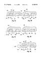
- FIGS. 5-18which describe the instant invention, and particularly to FIGS. 5 and 6, a pair of semiconductor devices 100 are shown in cross-section.
- the particular configuration of die 102, metallized leadframe 104, and die-to-lead attach methodmay be any of the wide variety of known constructions in the art.
- a chip-over-leads (COL) interior construction with inverted-J (IJ) outer leads 118is shown with inner leads 106 conductively connected to die pads 108 by wires 110.
- An intermediate lead portion 112is positioned during encapsulation, e.g.
- each leadis separated from adjacent leads by a spacing 122 which may vary along the length of the lead.
- the spacing 122 of the outer leads 118is uniform.
- the inner leads 106are completely enclosed within the polymeric package 120.
- the outer leads 118are completely outside of the polymeric package 120, and the intermediate lead portions 112, as formed, are within the bottom package surface 116 of the polymer package 120 and have a bottom lead surface 114 exposed.
- the outer leads 118, shown as inverted-J (IJ) leads, of one device 100may be joined to the intermediate lead portions 112 of another device if desired, or either the outer leads or intermediate lead portions may be joined to a circuit board, other electrical conduits, or another electrical apparatus.
- the spacing 122 of the polymeric package 120 between the lead edges 124 of the intermediate lead portions 112is partially cut away along and adjacent to the intermediate lead edges 124, exposing at least a portion of each edge.
- the excised portions 126may take several cross-sectional forms, as depicted generally in drawing FIGS. 7B, 7C, 7D or 7E.
- FIG. 7Ashows an intermediate lead portion 112 as formed along within the molded polymer package 120.
- the bottom lead surface 114is generally coplanar with the bottom package surface 116, depending upon the precision of lead placement within the mold.
- a thin coating of polymerwill sometimes cover the bottom lead surface 114 following removal of the device from the mold. In the manufacturing process, this coating will be subsequently removed to permit electrical connection to a conductor.
- the top lead surface 128 and lead edges 124are embedded in the polymer package 120.
- the lead thickness 132typically between about 0.5 and 3 mils
- the lead-to-lead spacing 122typically at least about 2-3 mils
- the lead-to-lead spacing 122 of the polymer package 120is chamfered adjacent the full lead thickness 132 of each lead edge 124 to expose the lead edges 124.
- the chamfer angle 130 of the excised chamfer portions 126may be between about 20 degrees and about 60 degrees, depending upon the available lead-to-lead distance between the intermediate lead portions 112.
- the excised chamfer portions 126are shallower, extending to a depth 134 of as little as only about 1/8 of the lead thickness 132.
- the depth 134is shown as about 1/2 of the lead thickness 132.
- a greater portion of the lead-to-lead spacing 122is removed, by which an interlead ridge 136 of polymeric package material extends downwardly to a distance 138 above the bottom lead surfaces 114.
- the ratio of distance 138 to lead thickness 132may be between about zero and about 1.0, although a preferred ratio will be between about 0.1 and about 0.6.
- FIG. 7Eshows another embodiment of the invention, in which the lead-to-lead spacing 122 is excised to a generally uniform depth 140.
- the ratio of depth 140 to the lead thickness 132may be between about 0.1 and about 0.8, but is preferably between about 0.1 and about 0.6.
- the excisionincludes not only chamfered portions of the polymer package 120 but the intermediate lead portion 112 itself.
- the exposed bottom lead surface 114 of the intermediate lead portion 112is depressed into the polymer package 120 a distance 45 which is up to about 1/2 of the original lead thickness 132.
- the distance 45is thus at least 1/2 of the original lead thickness 132.
- the chamfer angle 130may be between about 20 degrees and 60 degrees, and more preferably about 30-45 degrees. This embodiment results in easier alignment of other leads which are to be joined to the intermediate lead portions 112, the chamfer walls 149 acting as retainers of the inserted lead edges, not shown.
- the device 100may be electrically joined to another device, piggy-back style, which is already joined to e.g. a circuit board. Or, the device occupies a smaller amount of area for mounting purposes on a substrate.
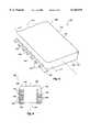
- FIGS. 8 and 9another version of the improved semiconductor device 100 is shown as a polymer package 120 having a top surface 117, a bottom package surface 116, two package sides 119, and ends 142.
- a general central axis 144passes lengthwise through the polymer package 120.
- the outer leads 118are truncated horizontal extensions of the intermediate lead portions 112, extending a short distance 146 outwardly, generally no more than about 8 to about 30 mils from the package sides 119. Preferably, distance 146 is between about 10 and about 20 mils.
- the outer leads 118have several surfaces which may be electrically connected to other leads or apparatus, including the upper lead surface 148 and the bottom lead surface 114.
- the semiconductor device 100 illustrated in drawing FIGS. 8 and 9may incorporate excision of the polymer package 120 along and adjacent the intermediate lead edges 124.
- any of the general excision shapes illustrated in drawing FIGS. 7B through 7Emay be used, in addition to the version of the invention illustrated in drawing FIG. 7A not having excised chamfer portions 126.
- the semiconductor device 100 of drawing FIGS. 10 and 11is similar to that illustrated in drawing FIGS. 8 and 9, except that it has no "outer” or external leads. Thus, it has the smallest "footprint" of the various embodiments, the footprint being merely the polymer package 120 itself. Electrical connections may be made between the bottom lead surfaces 114 and/or the end surfaces 150 of the intermediate lead portions 112.
- FIG. 11shows excised chamfer portions 126 of the lead-to-lead spacing 122 which have been excised or removed in accordance with the embodiments illustrated in drawing FIGS. 7B through 7E to provide the advantages previously outlined.
- FIGS. 12 and 13a small-footprint semiconductor device 100 is shown with intermediate lead portions 112 having bottom lead surfaces 114 generally coplanar with the bottom package surface 116 of the molded polymer package 120.
- the polymer package 120has a vertical groove 156 aligned with each outer lead 118 such that the outer lead may be bent upwardly to fit within the groove. Between each groove 156 is a column 157 of the polymer package 120.
- the semiconductor device 100will be no larger, or just barely larger, than the molded polymer package 120.
- outer leads 118A from the transfer molding processextend outwardly from the molded polymer package 120.
- Vertical grooves 156are premolded or formed after removal from a mold.
- Each outer lead 118Ais bent upwardly at bend 118B.
- the outer end 118Cis closely fitted within the vertical groove 156 near the top surface 117 of the molded polymer package 120, and a portion 118D of the lead in the area of bend 118B typically extends a short distance outwardly from the groove to provide a bonding surface for lateral electrical connection to another semiconductor device, electrical conduit, or electrical apparatus.
- Each vertical groove 156is shown as extending to the top surface 117 of the polymer package 120, with a groove depth 152 generally about equal to the lead thickness 132, and a groove width 154 slightly larger than the lead width 133, whereby the outer lead 118 will readily fit into the vertical groove 156.
- the semiconductor device 100has "surface" leads both on its bottom package surface 116 and on surfaces of the package sides 119 and/or ends 142.
- bottom lead surface 114which are to be bottom bonded may have adjacent chamfer portions 126 excised or removed as previously described in accordance with the embodiment illustrated in drawing FIGS. 7B-7E.
- the exemplary interior construction of the packaged device 100is shown as a chip-over-lead (COL) configuration, with chip or die 102 attached to inner lead 106 with an intervening insulative tape 158.
- the inventionrelates primarily to the configuration of an intermediate "surface" lead and the outer leads; the invention may be applied to any interior chip-lead configuration for reducing the overall size of the device 100 and providing both bottom and side/end lead bonding surfaces.
- FIGS. 14 and 15Another embodiment of the packaged semiconductor device 100 is shown in drawing FIGS. 14 and 15.
- the interior constructionis depicted as a chip-over-leads (COL) configuration with wires 110.
- the entire bottom lead surface 114 of each inner lead 106is coplanar with the bottom package surface 116 of the polymer package 120. Portions of bottom lead surface 114 which are to be bottom bonded may have adjacent chamfer portions 126 excised or removed as previously described in accordance with the embodiment illustrated in drawing FIGS. 7B-7E.
- outer leads 118are shown as short leads like those of the embodiment of drawing FIG. 8, they may take any useful form such as the inverted-J leads illustrated in drawing FIG. 5, the lateral leads of FIG. 12, or may be eliminated as outer leads as in drawing FIGS. 10 and 11, depending upon the apparatus to which the device 100 is to be connected.
- inner leads 106are primarily supported by their adhesive attachment to the insulative tape 158.
- FIG. 16shows a mold assembly 160 for encapsulating the die/leadframe assembly 162 in polymer to form the semiconductor package 120.
- the die/leadframe assembly 162is shown as including a die 102, leadframe 104, bond wires 110, and insulative tape 158.
- the mold assembly 160includes a top plate 160A and bottom plate 160B which are closed together to form a mold cavity 164 therein.
- Mold cavity 164is defined by an inner surface 166A of the top plate 160A and an inner surface 166B of the bottom plate 160B.
- a polymeric encapsulantis introduced as a hardenable fluid through openings (not shown) as known in the art.
- the top plate 160A and bottom plate 160Bare configured to produce a casting or package 120 (see other figures) with an intermediate lead portion 112 and outer lead 118 having bottom lead surfaces 114 which are coplanar with the bottom package surface 116 of the package.
- the mold assembly 160 illustrated in drawing FIG. 16may be used to form the packaged integrated circuit (IC) devices of the invention as described herein.
- the particular embodiment of FIGS. 12 and 13may have its alternating pattern of vertical grooves 156 and columns 157 produced after molding by cutting the vertical grooves 156 by an erosion process or other method known in the art.
- a cutting apparatus having a plurality of spinning saw bladesmay be used, for example.
- the particular groove/column patternmay also be produced in the molding step, using a mold assembly 170 as illustrated in drawing FIGS. 17 and 18.
- a wall 168 of the top plate 170A which is intersected by intermediate lead portions 112has a pattern of alternating mold grooves 176 and mold columns 178.
- the mold grooves 176are filled with encapsulant and become the package columns 157.
- the spaces occupied by the mold columns 178become the package grooves 156 into which the outer leads 118 are bent upwardly.
- FIG. 12depicts the package grooves 156 with square corners
- the preferred mold grooves 176have angled groove sides 180 for easy release of the hardened package from the mold cavity 172.
- the groove angle 182may be any angle which permits rapid package release, but will generally be in the range of 5-15 degrees, depending upon the surface roughness of the mold cavity 172 and the particular encapsulant being used.
- the steps involvedinclude:
- the attachment areas of the leadsmay be plated with e.g. tin to enhance adhesion in a subsequent solder bonding step.
- FIGS. 12 and 13Where a package of the embodiment of drawing FIGS. 12 and 13 is to be fabricated using cutting means to create the vertical grooves 156 in the package 120, such step will typically follow one of steps e, f, or g.
- the deflashing stepmay include deflashing of the grooves 156 in the package, as well as connection surfaces of the outer leads 118.
- an erosion process or other method known in the artmay be used. This step will follow removal from the mold step e or a subsequent step.
- the outer leadsare cut in conformance to the particular embodiment, as illustrated in drawing FIG. 5 (full inverted J-leads), FIG. 8 (abbreviated leads), FIG. 10 (leads cut at package surface), and FIG. 12 (abbreviated lead length).
- FIGS. 7B-7Eare representative only and illustrate preferred constructions.
- the inventionprovides a semiconductor package of reduced size, yet having leads for bottom and side/edge bonding or bottom and top bonding of the package.
- multiples of the devicemay be vertically stacked in parallel, and/or be electrically joined in a generally horizontal coplanar configuration.
- the inventionmay be applied to a three-dimension-lead (TDL) package having outer leads on the ends as well as the sides or top, together with bottom surface leads.
- TDLthree-dimension-lead
- the die/leadframe assembly shown and described hereinis exemplary only, and may include other elements such as additional dies and leadframes, heatsinks, dielectric layers, etc., as known in the art.
Landscapes
- Engineering & Computer Science (AREA)
- Physics & Mathematics (AREA)
- Microelectronics & Electronic Packaging (AREA)
- Power Engineering (AREA)
- Condensed Matter Physics & Semiconductors (AREA)
- General Physics & Mathematics (AREA)
- Computer Hardware Design (AREA)
- Geometry (AREA)
- Manufacturing & Machinery (AREA)
- Lead Frames For Integrated Circuits (AREA)
- Structures Or Materials For Encapsulating Or Coating Semiconductor Devices Or Solid State Devices (AREA)
Abstract
Description
Claims (11)
Priority Applications (1)
| Application Number | Priority Date | Filing Date | Title |
|---|---|---|---|
| US09/336,919US6146919A (en) | 1997-07-09 | 1999-06-21 | Package stack via bottom leaded plastic (BLP) packaging |
Applications Claiming Priority (2)
| Application Number | Priority Date | Filing Date | Title |
|---|---|---|---|
| US08/890,414US5986209A (en) | 1997-07-09 | 1997-07-09 | Package stack via bottom leaded plastic (BLP) packaging |
| US09/336,919US6146919A (en) | 1997-07-09 | 1999-06-21 | Package stack via bottom leaded plastic (BLP) packaging |
Related Parent Applications (1)
| Application Number | Title | Priority Date | Filing Date |
|---|---|---|---|
| US08/890,414DivisionUS5986209A (en) | 1997-07-09 | 1997-07-09 | Package stack via bottom leaded plastic (BLP) packaging |
Publications (1)
| Publication Number | Publication Date |
|---|---|
| US6146919Atrue US6146919A (en) | 2000-11-14 |
Family
ID=25396645
Family Applications (10)
| Application Number | Title | Priority Date | Filing Date |
|---|---|---|---|
| US08/890,414Expired - LifetimeUS5986209A (en) | 1997-07-09 | 1997-07-09 | Package stack via bottom leaded plastic (BLP) packaging |
| US09/330,105Expired - LifetimeUS6188021B1 (en) | 1997-07-09 | 1999-06-10 | Package stack via bottom leaded plastic (BLP) packaging |
| US09/336,919Expired - LifetimeUS6146919A (en) | 1997-07-09 | 1999-06-21 | Package stack via bottom leaded plastic (BLP) packaging |
| US09/337,628Expired - LifetimeUS6166328A (en) | 1997-07-09 | 1999-06-21 | Package stack via bottom leaded plastic (BLP) packaging |
| US09/336,925Expired - LifetimeUS6213747B1 (en) | 1997-07-09 | 1999-06-21 | Package stack via bottom leaded plastic (BLP) packaging |
| US09/641,623Expired - LifetimeUS6265660B1 (en) | 1997-07-09 | 2000-08-18 | Package stack via bottom leaded plastic (BLP) packaging |
| US09/819,909Expired - LifetimeUS6537051B2 (en) | 1997-07-09 | 2001-03-28 | Encapsulation mold with a castellated inner surface |
| US10/369,067Expired - Fee RelatedUS6899534B2 (en) | 1997-07-09 | 2003-02-18 | Mold assembly for a package stack via bottom-leaded plastic (blp) packaging |
| US11/138,756Expired - Fee RelatedUS7094046B2 (en) | 1997-07-09 | 2005-05-25 | Mold assembly for a package stack via bottom-leaded plastic (BLP) packaging |
| US11/338,384AbandonedUS20060118938A1 (en) | 1997-07-09 | 2006-01-24 | Mold assembly, method and a package stack via bottom-leaded plastic (BLP) packaging |
Family Applications Before (2)
| Application Number | Title | Priority Date | Filing Date |
|---|---|---|---|
| US08/890,414Expired - LifetimeUS5986209A (en) | 1997-07-09 | 1997-07-09 | Package stack via bottom leaded plastic (BLP) packaging |
| US09/330,105Expired - LifetimeUS6188021B1 (en) | 1997-07-09 | 1999-06-10 | Package stack via bottom leaded plastic (BLP) packaging |
Family Applications After (7)
| Application Number | Title | Priority Date | Filing Date |
|---|---|---|---|
| US09/337,628Expired - LifetimeUS6166328A (en) | 1997-07-09 | 1999-06-21 | Package stack via bottom leaded plastic (BLP) packaging |
| US09/336,925Expired - LifetimeUS6213747B1 (en) | 1997-07-09 | 1999-06-21 | Package stack via bottom leaded plastic (BLP) packaging |
| US09/641,623Expired - LifetimeUS6265660B1 (en) | 1997-07-09 | 2000-08-18 | Package stack via bottom leaded plastic (BLP) packaging |
| US09/819,909Expired - LifetimeUS6537051B2 (en) | 1997-07-09 | 2001-03-28 | Encapsulation mold with a castellated inner surface |
| US10/369,067Expired - Fee RelatedUS6899534B2 (en) | 1997-07-09 | 2003-02-18 | Mold assembly for a package stack via bottom-leaded plastic (blp) packaging |
| US11/138,756Expired - Fee RelatedUS7094046B2 (en) | 1997-07-09 | 2005-05-25 | Mold assembly for a package stack via bottom-leaded plastic (BLP) packaging |
| US11/338,384AbandonedUS20060118938A1 (en) | 1997-07-09 | 2006-01-24 | Mold assembly, method and a package stack via bottom-leaded plastic (BLP) packaging |
Country Status (1)
| Country | Link |
|---|---|
| US (10) | US5986209A (en) |
Cited By (13)
| Publication number | Priority date | Publication date | Assignee | Title |
|---|---|---|---|---|
| US20020100963A1 (en)* | 2001-01-26 | 2002-08-01 | Mitsubishi Denki Kabushiki Kaisha | Semiconductor package and semiconductor device |
| US20030129271A1 (en)* | 1997-07-09 | 2003-07-10 | Tandy Patrick W. | Package stack via bottom-leaded plastic (BLP) packaging |
| US6667544B1 (en)* | 2000-06-30 | 2003-12-23 | Amkor Technology, Inc. | Stackable package having clips for fastening package and tool for opening clips |
| US6753599B2 (en)* | 2001-02-12 | 2004-06-22 | Samsung Electronics Co., Ltd. | Semiconductor package and mounting structure on substrate thereof and stack structure thereof |
| US20050263311A1 (en)* | 2004-05-28 | 2005-12-01 | Chen-Jung Tsai | Method and apparatus for stacking electrical components using outer lead portions and exposed inner lead portions to provide interconnection |
| US20070028685A1 (en)* | 2004-10-08 | 2007-02-08 | Yamaha Corporation | Physical quantity sensor and manufacturing method therefor |
| US20070210441A1 (en)* | 2006-03-08 | 2007-09-13 | Micron Technology, Inc. | Microelectronic device assemblies including assemblies with recurved leadframes, and associated methods |
| US20070220988A1 (en)* | 2004-10-01 | 2007-09-27 | Kenichi Shirasaka | Physical Quantity Sensor and Lead Frame Used for Same |
| US20080012110A1 (en)* | 2006-07-17 | 2008-01-17 | Micron Technology, Inc. | Microelectronic packages with leadframes, including leadframes configured for stacked die packages, and associated systems and methods |
| CN100370611C (en)* | 2004-02-03 | 2008-02-20 | 旺宏电子股份有限公司 | Electronic component stack structure |
| US20080277770A1 (en)* | 2007-04-27 | 2008-11-13 | Kabushiki Kaisha Toshiba | Semiconductor device |
| US7843050B2 (en) | 2007-07-24 | 2010-11-30 | Micron Technology, Inc. | Microelectronic die packages with metal leads, including metal leads for stacked die packages, and associated systems and methods |
| US7947529B2 (en) | 2007-08-16 | 2011-05-24 | Micron Technology, Inc. | Microelectronic die packages with leadframes, including leadframe-based interposer for stacked die packages, and associated systems and methods |
Families Citing this family (202)
| Publication number | Priority date | Publication date | Assignee | Title |
|---|---|---|---|---|
| US6165819A (en)* | 1992-10-20 | 2000-12-26 | Fujitsu Limited | Semiconductor device, method of producing semiconductor device and semiconductor device mounting structure |
| KR100242393B1 (en)* | 1996-11-22 | 2000-02-01 | 김영환 | Semiconductor Package and Manufacturing Method |
| JPH1197619A (en)* | 1997-07-25 | 1999-04-09 | Oki Electric Ind Co Ltd | Semiconductor device, manufacture thereof and mounting thereof |
| US6342731B1 (en)* | 1997-12-31 | 2002-01-29 | Micron Technology, Inc. | Vertically mountable semiconductor device, assembly, and methods |
| US6429528B1 (en)* | 1998-02-27 | 2002-08-06 | Micron Technology, Inc. | Multichip semiconductor package |
| JP4342013B2 (en)* | 1998-05-06 | 2009-10-14 | 株式会社ハイニックスセミコンダクター | BLP stack of ultra-high integrated circuit and manufacturing method thereof |
| JP3842444B2 (en)* | 1998-07-24 | 2006-11-08 | 富士通株式会社 | Manufacturing method of semiconductor device |
| US6323060B1 (en) | 1999-05-05 | 2001-11-27 | Dense-Pac Microsystems, Inc. | Stackable flex circuit IC package and method of making same |
| JP3575001B2 (en) | 1999-05-07 | 2004-10-06 | アムコー テクノロジー コリア インコーポレーティド | Semiconductor package and manufacturing method thereof |
| USRE40112E1 (en) | 1999-05-20 | 2008-02-26 | Amkor Technology, Inc. | Semiconductor package and method for fabricating the same |
| JP3398721B2 (en) | 1999-05-20 | 2003-04-21 | アムコー テクノロジー コリア インコーポレーティド | Semiconductor package and manufacturing method thereof |
| KR100426494B1 (en)* | 1999-12-20 | 2004-04-13 | 앰코 테크놀로지 코리아 주식회사 | Semiconductor package and its manufacturing method |
| US6262895B1 (en) | 2000-01-13 | 2001-07-17 | John A. Forthun | Stackable chip package with flex carrier |
| US6320251B1 (en)* | 2000-01-18 | 2001-11-20 | Amkor Technology, Inc. | Stackable package for an integrated circuit |
| US6404046B1 (en) | 2000-02-03 | 2002-06-11 | Amkor Technology, Inc. | Module of stacked integrated circuit packages including an interposer |
| US6558600B1 (en) | 2000-05-04 | 2003-05-06 | Micron Technology, Inc. | Method for packaging microelectronic substrates |
| AU2001259681A1 (en) | 2000-05-08 | 2001-11-20 | Micron Technology, Inc. | Method and apparatus for distributing mold material in a mold for packaging microelectronic devices |
| US6518659B1 (en) | 2000-05-08 | 2003-02-11 | Amkor Technology, Inc. | Stackable package having a cavity and a lid for an electronic device |
| US6424031B1 (en) | 2000-05-08 | 2002-07-23 | Amkor Technology, Inc. | Stackable package with heat sink |
| US6589820B1 (en) | 2000-06-16 | 2003-07-08 | Micron Technology, Inc. | Method and apparatus for packaging a microelectronic die |
| US6552910B1 (en) | 2000-06-28 | 2003-04-22 | Micron Technology, Inc. | Stacked-die assemblies with a plurality of microelectronic devices and methods of manufacture |
| US6560117B2 (en) | 2000-06-28 | 2003-05-06 | Micron Technology, Inc. | Packaged microelectronic die assemblies and methods of manufacture |
| US6365434B1 (en) | 2000-06-28 | 2002-04-02 | Micron Technology, Inc. | Method and apparatus for reduced flash encapsulation of microelectronic devices |
| US6576494B1 (en) | 2000-06-28 | 2003-06-10 | Micron Technology, Inc. | Recessed encapsulated microelectronic devices and methods for formation |
| JP2002026168A (en)* | 2000-06-30 | 2002-01-25 | Hitachi Ltd | Semiconductor device and method of manufacturing the same |
| US7298031B1 (en) | 2000-08-09 | 2007-11-20 | Micron Technology, Inc. | Multiple substrate microelectronic devices and methods of manufacture |
| US7273769B1 (en) | 2000-08-16 | 2007-09-25 | Micron Technology, Inc. | Method and apparatus for removing encapsulating material from a packaged microelectronic device |
| US6483044B1 (en) | 2000-08-23 | 2002-11-19 | Micron Technology, Inc. | Interconnecting substrates for electrical coupling of microelectronic components |
| US6607937B1 (en)* | 2000-08-23 | 2003-08-19 | Micron Technology, Inc. | Stacked microelectronic dies and methods for stacking microelectronic dies |
| US7183138B2 (en)* | 2000-08-23 | 2007-02-27 | Micron Technology, Inc. | Method and apparatus for decoupling conductive portions of a microelectronic device package |
| US6979595B1 (en) | 2000-08-24 | 2005-12-27 | Micron Technology, Inc. | Packaged microelectronic devices with pressure release elements and methods for manufacturing and using such packaged microelectronic devices |
| US6838760B1 (en) | 2000-08-28 | 2005-01-04 | Micron Technology, Inc. | Packaged microelectronic devices with interconnecting units |
| US6787388B1 (en)* | 2000-09-07 | 2004-09-07 | Stmicroelectronics, Inc. | Surface mount package with integral electro-static charge dissipating ring using lead frame as ESD device |
| JP3405456B2 (en)* | 2000-09-11 | 2003-05-12 | 沖電気工業株式会社 | Semiconductor device, method of manufacturing semiconductor device, stack type semiconductor device, and method of manufacturing stack type semiconductor device |
| US6564454B1 (en) | 2000-12-28 | 2003-05-20 | Amkor Technology, Inc. | Method of making and stacking a semiconductor package |
| US6448506B1 (en) | 2000-12-28 | 2002-09-10 | Amkor Technology, Inc. | Semiconductor package and circuit board for making the package |
| US6664649B2 (en)* | 2001-02-28 | 2003-12-16 | Siliconware Precision Industries Co., Ltd. | Lead-on-chip type of semiconductor package with embedded heat sink |
| US6777786B2 (en)* | 2001-03-12 | 2004-08-17 | Fairchild Semiconductor Corporation | Semiconductor device including stacked dies mounted on a leadframe |
| US6564979B2 (en) | 2001-07-18 | 2003-05-20 | Micron Technology, Inc. | Method and apparatus for dispensing adhesive on microelectronic substrate supports |
| SG111919A1 (en) | 2001-08-29 | 2005-06-29 | Micron Technology Inc | Packaged microelectronic devices and methods of forming same |
| US6548376B2 (en) | 2001-08-30 | 2003-04-15 | Micron Technology, Inc. | Methods of thinning microelectronic workpieces |
| US20030042615A1 (en) | 2001-08-30 | 2003-03-06 | Tongbi Jiang | Stacked microelectronic devices and methods of fabricating same |
| US6969918B1 (en) | 2001-08-30 | 2005-11-29 | Micron Technology, Inc. | System for fabricating semiconductor components using mold cavities having runners configured to minimize venting |
| US6747348B2 (en)* | 2001-10-16 | 2004-06-08 | Micron Technology, Inc. | Apparatus and method for leadless packaging of semiconductor devices |
| US6956284B2 (en) | 2001-10-26 | 2005-10-18 | Staktek Group L.P. | Integrated circuit stacking system and method |
| US7310458B2 (en) | 2001-10-26 | 2007-12-18 | Staktek Group L.P. | Stacked module systems and methods |
| US7026708B2 (en) | 2001-10-26 | 2006-04-11 | Staktek Group L.P. | Low profile chip scale stacking system and method |
| US7656678B2 (en) | 2001-10-26 | 2010-02-02 | Entorian Technologies, Lp | Stacked module systems |
| US7053478B2 (en) | 2001-10-26 | 2006-05-30 | Staktek Group L.P. | Pitch change and chip scale stacking system |
| US20060255446A1 (en) | 2001-10-26 | 2006-11-16 | Staktek Group, L.P. | Stacked modules and method |
| US20030234443A1 (en) | 2001-10-26 | 2003-12-25 | Staktek Group, L.P. | Low profile stacking system and method |
| US7485951B2 (en)* | 2001-10-26 | 2009-02-03 | Entorian Technologies, Lp | Modularized die stacking system and method |
| US7371609B2 (en) | 2001-10-26 | 2008-05-13 | Staktek Group L.P. | Stacked module systems and methods |
| US7202555B2 (en) | 2001-10-26 | 2007-04-10 | Staktek Group L.P. | Pitch change and chip scale stacking system and method |
| US6940729B2 (en)* | 2001-10-26 | 2005-09-06 | Staktek Group L.P. | Integrated circuit stacking system and method |
| US6914324B2 (en) | 2001-10-26 | 2005-07-05 | Staktek Group L.P. | Memory expansion and chip scale stacking system and method |
| US7081373B2 (en) | 2001-12-14 | 2006-07-25 | Staktek Group, L.P. | CSP chip stack with flex circuit |
| US6750547B2 (en)* | 2001-12-26 | 2004-06-15 | Micron Technology, Inc. | Multi-substrate microelectronic packages and methods for manufacture |
| US6870276B1 (en)* | 2001-12-26 | 2005-03-22 | Micron Technology, Inc. | Apparatus for supporting microelectronic substrates |
| JP2003204039A (en)* | 2002-01-04 | 2003-07-18 | Mitsubishi Electric Corp | Semiconductor device |
| US6896760B1 (en)* | 2002-01-16 | 2005-05-24 | Micron Technology, Inc. | Fabrication of stacked microelectronic devices |
| US6622380B1 (en) | 2002-02-12 | 2003-09-23 | Micron Technology, Inc. | Methods for manufacturing microelectronic devices and methods for mounting microelectronic packages to circuit boards |
| US7198693B1 (en) | 2002-02-20 | 2007-04-03 | Micron Technology, Inc. | Microelectronic device having a plurality of stacked dies and methods for manufacturing such microelectronic assemblies |
| US7109588B2 (en) | 2002-04-04 | 2006-09-19 | Micron Technology, Inc. | Method and apparatus for attaching microelectronic substrates and support members |
| SG111069A1 (en)* | 2002-06-18 | 2005-05-30 | Micron Technology Inc | Semiconductor devices including peripherally located bond pads, assemblies, packages, and methods |
| SG107595A1 (en)* | 2002-06-18 | 2004-12-29 | Micron Technology Inc | Semiconductor devices and semiconductor device components with peripherally located, castellated contacts, assembles and packages including such semiconductor devices or packages and associated methods |
| US20040000703A1 (en)* | 2002-06-27 | 2004-01-01 | Jui-Chung Lee | Semiconductor package body having a lead frame with enhanced heat dissipation |
| US6903001B2 (en)* | 2002-07-18 | 2005-06-07 | Micron Technology Inc. | Techniques to create low K ILD for BEOL |
| US7067905B2 (en)* | 2002-08-08 | 2006-06-27 | Micron Technology, Inc. | Packaged microelectronic devices including first and second casings |
| SG120879A1 (en) | 2002-08-08 | 2006-04-26 | Micron Technology Inc | Packaged microelectronic components |
| SG127684A1 (en)* | 2002-08-19 | 2006-12-29 | Micron Technology Inc | Packaged microelectronic component assemblies |
| US6740546B2 (en)* | 2002-08-21 | 2004-05-25 | Micron Technology, Inc. | Packaged microelectronic devices and methods for assembling microelectronic devices |
| US6845901B2 (en)* | 2002-08-22 | 2005-01-25 | Micron Technology, Inc. | Apparatus and method for depositing and reflowing solder paste on a microelectronic workpiece |
| SG114585A1 (en) | 2002-11-22 | 2005-09-28 | Micron Technology Inc | Packaged microelectronic component assemblies |
| US7132734B2 (en)* | 2003-01-06 | 2006-11-07 | Micron Technology, Inc. | Microelectronic component assemblies and microelectronic component lead frame structures |
| US6879050B2 (en)* | 2003-02-11 | 2005-04-12 | Micron Technology, Inc. | Packaged microelectronic devices and methods for packaging microelectronic devices |
| SG143931A1 (en)* | 2003-03-04 | 2008-07-29 | Micron Technology Inc | Microelectronic component assemblies employing lead frames having reduced-thickness inner lengths |
| US7183485B2 (en)* | 2003-03-11 | 2007-02-27 | Micron Technology, Inc. | Microelectronic component assemblies having lead frames adapted to reduce package bow |
| SG137651A1 (en)* | 2003-03-14 | 2007-12-28 | Micron Technology Inc | Microelectronic devices and methods for packaging microelectronic devices |
| US6921860B2 (en) | 2003-03-18 | 2005-07-26 | Micron Technology, Inc. | Microelectronic component assemblies having exposed contacts |
| TWI338927B (en)* | 2003-04-02 | 2011-03-11 | United Test And Assembly Ct | Multi-chip ball grid array package and method of manufacture |
| SG143932A1 (en)* | 2003-05-30 | 2008-07-29 | Micron Technology Inc | Packaged microelectronic devices and methods of packaging microelectronic devices |
| US7309923B2 (en)* | 2003-06-16 | 2007-12-18 | Sandisk Corporation | Integrated circuit package having stacked integrated circuits and method therefor |
| US6984881B2 (en)* | 2003-06-16 | 2006-01-10 | Sandisk Corporation | Stackable integrated circuit package and method therefor |
| US7227095B2 (en) | 2003-08-06 | 2007-06-05 | Micron Technology, Inc. | Wire bonders and methods of wire-bonding |
| US7071421B2 (en) | 2003-08-29 | 2006-07-04 | Micron Technology, Inc. | Stacked microfeature devices and associated methods |
| US7368810B2 (en) | 2003-08-29 | 2008-05-06 | Micron Technology, Inc. | Invertible microfeature device packages |
| US6924655B2 (en)* | 2003-09-03 | 2005-08-02 | Micron Technology, Inc. | Probe card for use with microelectronic components, and methods for making same |
| US7542304B2 (en) | 2003-09-15 | 2009-06-02 | Entorian Technologies, Lp | Memory expansion and integrated circuit stacking system and method |
| SG120123A1 (en)* | 2003-09-30 | 2006-03-28 | Micron Technology Inc | Castellated chip-scale packages and methods for fabricating the same |
| TWI228303B (en)* | 2003-10-29 | 2005-02-21 | Advanced Semiconductor Eng | Semiconductor package, method for manufacturing the same and lead frame for use in the same |
| SG153627A1 (en)* | 2003-10-31 | 2009-07-29 | Micron Technology Inc | Reduced footprint packaged microelectronic components and methods for manufacturing such microelectronic components |
| US6977431B1 (en) | 2003-11-05 | 2005-12-20 | Amkor Technology, Inc. | Stackable semiconductor package and manufacturing method thereof |
| US8084866B2 (en) | 2003-12-10 | 2011-12-27 | Micron Technology, Inc. | Microelectronic devices and methods for filling vias in microelectronic devices |
| US20050104171A1 (en)* | 2003-11-13 | 2005-05-19 | Benson Peter A. | Microelectronic devices having conductive complementary structures and methods of manufacturing microelectronic devices having conductive complementary structures |
| US7091124B2 (en) | 2003-11-13 | 2006-08-15 | Micron Technology, Inc. | Methods for forming vias in microelectronic devices, and methods for packaging microelectronic devices |
| US7633140B2 (en)* | 2003-12-09 | 2009-12-15 | Alpha And Omega Semiconductor Incorporated | Inverted J-lead for power devices |
| US20070145548A1 (en)* | 2003-12-22 | 2007-06-28 | Amkor Technology, Inc. | Stack-type semiconductor package and manufacturing method thereof |
| US7009296B1 (en) | 2004-01-15 | 2006-03-07 | Amkor Technology, Inc. | Semiconductor package with substrate coupled to a peripheral side surface of a semiconductor die |
| US7851899B2 (en)* | 2004-04-02 | 2010-12-14 | Utac - United Test And Assembly Test Center Ltd. | Multi-chip ball grid array package and method of manufacture |
| SG145547A1 (en)* | 2004-07-23 | 2008-09-29 | Micron Technology Inc | Microelectronic component assemblies with recessed wire bonds and methods of making same |
| US7381593B2 (en)* | 2004-08-05 | 2008-06-03 | St Assembly Test Services Ltd. | Method and apparatus for stacked die packaging |
| US7632747B2 (en)* | 2004-08-19 | 2009-12-15 | Micron Technology, Inc. | Conductive structures for microfeature devices and methods for fabricating microfeature devices |
| US7602618B2 (en)* | 2004-08-25 | 2009-10-13 | Micron Technology, Inc. | Methods and apparatuses for transferring heat from stacked microfeature devices |
| US7095122B2 (en)* | 2004-09-01 | 2006-08-22 | Micron Technology, Inc. | Reduced-dimension microelectronic component assemblies with wire bonds and methods of making same |
| US7157310B2 (en)* | 2004-09-01 | 2007-01-02 | Micron Technology, Inc. | Methods for packaging microfeature devices and microfeature devices formed by such methods |
| US7522421B2 (en) | 2004-09-03 | 2009-04-21 | Entorian Technologies, Lp | Split core circuit module |
| US7423885B2 (en) | 2004-09-03 | 2008-09-09 | Entorian Technologies, Lp | Die module system |
| US7606049B2 (en) | 2004-09-03 | 2009-10-20 | Entorian Technologies, Lp | Module thermal management system and method |
| US7760513B2 (en) | 2004-09-03 | 2010-07-20 | Entorian Technologies Lp | Modified core for circuit module system and method |
| US7446410B2 (en)* | 2004-09-03 | 2008-11-04 | Entorian Technologies, Lp | Circuit module with thermal casing systems |
| US7468893B2 (en) | 2004-09-03 | 2008-12-23 | Entorian Technologies, Lp | Thin module system and method |
| US20060050492A1 (en) | 2004-09-03 | 2006-03-09 | Staktek Group, L.P. | Thin module system and method |
| US7579687B2 (en)* | 2004-09-03 | 2009-08-25 | Entorian Technologies, Lp | Circuit module turbulence enhancement systems and methods |
| US7616452B2 (en) | 2004-09-03 | 2009-11-10 | Entorian Technologies, Lp | Flex circuit constructions for high capacity circuit module systems and methods |
| US7542297B2 (en) | 2004-09-03 | 2009-06-02 | Entorian Technologies, Lp | Optimized mounting area circuit module system and method |
| US7324352B2 (en) | 2004-09-03 | 2008-01-29 | Staktek Group L.P. | High capacity thin module system and method |
| US7511968B2 (en) | 2004-09-03 | 2009-03-31 | Entorian Technologies, Lp | Buffered thin module system and method |
| US7606040B2 (en) | 2004-09-03 | 2009-10-20 | Entorian Technologies, Lp | Memory module system and method |
| US20060053345A1 (en)* | 2004-09-03 | 2006-03-09 | Staktek Group L.P. | Thin module system and method |
| US7443023B2 (en) | 2004-09-03 | 2008-10-28 | Entorian Technologies, Lp | High capacity thin module system |
| US7289327B2 (en) | 2006-02-27 | 2007-10-30 | Stakick Group L.P. | Active cooling methods and apparatus for modules |
| US7606050B2 (en) | 2004-09-03 | 2009-10-20 | Entorian Technologies, Lp | Compact module system and method |
| US7211510B2 (en)* | 2004-09-09 | 2007-05-01 | Advanced Bionics Corporation | Stacking circuit elements |
| TWM269570U (en)* | 2004-12-24 | 2005-07-01 | Domintech Co Ltd | Improved structure of stacked chip package |
| US7309914B2 (en) | 2005-01-20 | 2007-12-18 | Staktek Group L.P. | Inverted CSP stacking system and method |
| CN2779618Y (en)* | 2005-01-21 | 2006-05-10 | 资重兴 | Laminative encapsulation chip structure improvement |
| US8278751B2 (en) | 2005-02-08 | 2012-10-02 | Micron Technology, Inc. | Methods of adhering microfeature workpieces, including a chip, to a support member |
| US8395251B2 (en)* | 2005-05-12 | 2013-03-12 | Stats Chippac Ltd. | Integrated circuit package to package stacking system |
| US7518224B2 (en)* | 2005-05-16 | 2009-04-14 | Stats Chippac Ltd. | Offset integrated circuit package-on-package stacking system |
| US7746656B2 (en)* | 2005-05-16 | 2010-06-29 | Stats Chippac Ltd. | Offset integrated circuit package-on-package stacking system |
| US7033861B1 (en) | 2005-05-18 | 2006-04-25 | Staktek Group L.P. | Stacked module systems and method |
| US20060267173A1 (en)* | 2005-05-26 | 2006-11-30 | Sandisk Corporation | Integrated circuit package having stacked integrated circuits and method therefor |
| WO2007005263A2 (en)* | 2005-06-30 | 2007-01-11 | Fairchild Semiconductor Corporation | Semiconductor die package and method for making the same |
| SG130055A1 (en)* | 2005-08-19 | 2007-03-20 | Micron Technology Inc | Microelectronic devices, stacked microelectronic devices, and methods for manufacturing microelectronic devices |
| SG130061A1 (en)* | 2005-08-24 | 2007-03-20 | Micron Technology Inc | Microelectronic devices and microelectronic support devices, and associated assemblies and methods |
| SG130066A1 (en)* | 2005-08-26 | 2007-03-20 | Micron Technology Inc | Microelectronic device packages, stacked microelectronic device packages, and methods for manufacturing microelectronic devices |
| US7807505B2 (en) | 2005-08-30 | 2010-10-05 | Micron Technology, Inc. | Methods for wafer-level packaging of microfeature devices and microfeature devices formed using such methods |
| US7745944B2 (en) | 2005-08-31 | 2010-06-29 | Micron Technology, Inc. | Microelectronic devices having intermediate contacts for connection to interposer substrates, and associated methods of packaging microelectronic devices with intermediate contacts |
| US7622377B2 (en) | 2005-09-01 | 2009-11-24 | Micron Technology, Inc. | Microfeature workpiece substrates having through-substrate vias, and associated methods of formation |
| US7485969B2 (en)* | 2005-09-01 | 2009-02-03 | Micron Technology, Inc. | Stacked microelectronic devices and methods for manufacturing microelectronic devices |
| US20070045807A1 (en)* | 2005-09-01 | 2007-03-01 | Micron Technology, Inc. | Microelectronic devices and methods for manufacturing microelectronic devices |
| US7576995B2 (en) | 2005-11-04 | 2009-08-18 | Entorian Technologies, Lp | Flex circuit apparatus and method for adding capacitance while conserving circuit board surface area |
| US20070148820A1 (en)* | 2005-12-22 | 2007-06-28 | Micron Technology, Inc. | Microelectronic devices and methods for manufacturing microelectronic devices |
| SG133445A1 (en) | 2005-12-29 | 2007-07-30 | Micron Technology Inc | Methods for packaging microelectronic devices and microelectronic devices formed using such methods |
| US7304382B2 (en) | 2006-01-11 | 2007-12-04 | Staktek Group L.P. | Managed memory component |
| US7605454B2 (en) | 2006-01-11 | 2009-10-20 | Entorian Technologies, Lp | Memory card and method for devising |
| US7508069B2 (en) | 2006-01-11 | 2009-03-24 | Entorian Technologies, Lp | Managed memory component |
| US7508058B2 (en) | 2006-01-11 | 2009-03-24 | Entorian Technologies, Lp | Stacked integrated circuit module |
| US7608920B2 (en) | 2006-01-11 | 2009-10-27 | Entorian Technologies, Lp | Memory card and method for devising |
| US7511969B2 (en) | 2006-02-02 | 2009-03-31 | Entorian Technologies, Lp | Composite core circuit module system and method |
| SG135074A1 (en) | 2006-02-28 | 2007-09-28 | Micron Technology Inc | Microelectronic devices, stacked microelectronic devices, and methods for manufacturing such devices |
| EP2657976B1 (en)* | 2006-03-16 | 2018-12-26 | Fujitsu Limited | Compound Semiconductor Device and Manufacturing Method of the Same |
| SG136009A1 (en) | 2006-03-29 | 2007-10-29 | Micron Technology Inc | Packaged microelectronic devices recessed in support member cavities, and associated methods |
| US7910385B2 (en) | 2006-05-12 | 2011-03-22 | Micron Technology, Inc. | Method of fabricating microelectronic devices |
| SG138501A1 (en)* | 2006-07-05 | 2008-01-28 | Micron Technology Inc | Lead frames, microelectronic devices with lead frames, and methods for manufacturing lead frames and microelectronic devices with lead frames |
| US7535086B2 (en)* | 2006-08-03 | 2009-05-19 | Stats Chippac Ltd. | Integrated circuit package-on-package stacking system |
| US7868440B2 (en) | 2006-08-25 | 2011-01-11 | Micron Technology, Inc. | Packaged microdevices and methods for manufacturing packaged microdevices |
| KR20080022452A (en)* | 2006-09-06 | 2008-03-11 | 삼성전자주식회사 | PPO package and its manufacturing method |
| KR100833184B1 (en)* | 2006-09-21 | 2008-05-28 | 삼성전자주식회사 | Stacked Semiconductor Packages |
| US7468553B2 (en) | 2006-10-20 | 2008-12-23 | Entorian Technologies, Lp | Stackable micropackages and stacked modules |
| US7417310B2 (en) | 2006-11-02 | 2008-08-26 | Entorian Technologies, Lp | Circuit module having force resistant construction |
| SG143098A1 (en) | 2006-12-04 | 2008-06-27 | Micron Technology Inc | Packaged microelectronic devices and methods for manufacturing packaged microelectronic devices |
| US8163600B2 (en)* | 2006-12-28 | 2012-04-24 | Stats Chippac Ltd. | Bridge stack integrated circuit package-on-package system |
| US7729131B2 (en)* | 2007-01-05 | 2010-06-01 | Apple Inc. | Multiple circuit board arrangements in electronic devices |
| US9466545B1 (en) | 2007-02-21 | 2016-10-11 | Amkor Technology, Inc. | Semiconductor package in package |
| US7833456B2 (en) | 2007-02-23 | 2010-11-16 | Micron Technology, Inc. | Systems and methods for compressing an encapsulant adjacent a semiconductor workpiece |
| US7750449B2 (en)* | 2007-03-13 | 2010-07-06 | Micron Technology, Inc. | Packaged semiconductor components having substantially rigid support members and methods of packaging semiconductor components |
| US7955898B2 (en) | 2007-03-13 | 2011-06-07 | Micron Technology, Inc. | Packaged microelectronic devices and methods for manufacturing packaged microelectronic devices |
| DE102007018914B4 (en)* | 2007-04-19 | 2019-01-17 | Infineon Technologies Ag | Semiconductor device with a semiconductor chip stack and method for producing the same |
| US20080258282A1 (en)* | 2007-04-23 | 2008-10-23 | Hua Yang | Lead frame free package and method of making |
| US20090004783A1 (en)* | 2007-06-27 | 2009-01-01 | Ming Hsun Lee | Method of package stacking using unbalanced molded tsop |
| US20090001529A1 (en)* | 2007-06-27 | 2009-01-01 | Ming Hsun Lee | Package stacking using unbalanced molded tsop |
| US7893545B2 (en)* | 2007-07-18 | 2011-02-22 | Infineon Technologies Ag | Semiconductor device |
| SG149725A1 (en)* | 2007-07-24 | 2009-02-27 | Micron Technology Inc | Thin semiconductor die packages and associated systems and methods |
| SG149724A1 (en)* | 2007-07-24 | 2009-02-27 | Micron Technology Inc | Semicoductor dies with recesses, associated leadframes, and associated systems and methods |
| US7830022B2 (en)* | 2007-10-22 | 2010-11-09 | Infineon Technologies Ag | Semiconductor package |
| US9147649B2 (en)* | 2008-01-24 | 2015-09-29 | Infineon Technologies Ag | Multi-chip module |
| US7863102B2 (en)* | 2008-02-22 | 2011-01-04 | Stats Chippac Ltd. | Integrated circuit package system with external interconnects within a die platform |
| JP5103245B2 (en) | 2008-03-31 | 2012-12-19 | ルネサスエレクトロニクス株式会社 | Semiconductor device |
| US7872332B2 (en)* | 2008-09-11 | 2011-01-18 | Micron Technology, Inc. | Interconnect structures for stacked dies, including penetrating structures for through-silicon vias, and associated systems and methods |
| US20110147910A1 (en)* | 2009-12-21 | 2011-06-23 | Micron Technology, Inc. | Method for stacking die in thin, small-outline package |
| DE102010026312B4 (en)* | 2010-07-06 | 2022-10-20 | Phoenix Contact Gmbh & Co. Kg | Connection contact and method for producing connection contacts |
| JP2012204667A (en)* | 2011-03-25 | 2012-10-22 | Toshiba Corp | Semiconductor device |
| WO2014188632A1 (en)* | 2013-05-23 | 2014-11-27 | パナソニック株式会社 | Semiconductor device having heat dissipation structure and laminate of semiconductor devices |
| KR102186146B1 (en) | 2014-01-03 | 2020-12-03 | 삼성전기주식회사 | Package board, method of manufacturing the same and semiconductor package using the same |
| US20150257300A1 (en)* | 2014-03-10 | 2015-09-10 | Kabushiki Kaisha Toshiba | Electronic device |
| US20160071788A1 (en)* | 2014-03-17 | 2016-03-10 | Texas Instruments Incorporated | Packaged semiconductor devices having solderable lead surfaces exposed by grooves in package compound |
| KR102333083B1 (en) | 2014-05-30 | 2021-12-01 | 삼성전기주식회사 | Package board and method for manufacturing the same |
| KR102254874B1 (en) | 2014-05-30 | 2021-05-24 | 삼성전기주식회사 | Package board and method for manufacturing the same |
| KR102262907B1 (en) | 2014-05-30 | 2021-06-09 | 삼성전기주식회사 | Package substrate, package, package on package and maunfacutring method of package substrate |
| KR102194719B1 (en) | 2014-06-12 | 2020-12-23 | 삼성전기주식회사 | Package board and package using the same |
| KR20150142520A (en) | 2014-06-12 | 2015-12-22 | 삼성전기주식회사 | Package board and package using the same |
| KR102240704B1 (en) | 2014-07-15 | 2021-04-15 | 삼성전기주식회사 | Package board, method of manufacturing the same and stack type package using the therof |
| US9392691B2 (en) | 2014-07-16 | 2016-07-12 | International Business Machines Corporation | Multi-stacked electronic device with defect-free solder connection |
| KR102194722B1 (en) | 2014-09-17 | 2020-12-23 | 삼성전기주식회사 | Package board, method for manufacturing the same and package on package having the thereof |
| KR102016475B1 (en) | 2014-10-21 | 2019-09-02 | 삼성전기주식회사 | Semiconductor, method of manufacturing the same and stacked type package using therof |
| KR102425753B1 (en) | 2015-06-01 | 2022-07-28 | 삼성전기주식회사 | Printed circuit board, method for manufacturing the same and semiconductor package having the thereof |
| US20200035577A1 (en)* | 2018-07-26 | 2020-01-30 | Texas Instruments Incorporated | Packaged integrated circuit |
| US11682609B2 (en)* | 2019-06-29 | 2023-06-20 | Texas Instruments Incorporated | Three-dimensional functional integration |
| CN111090058A (en)* | 2019-11-22 | 2020-05-01 | 珠海格力电器股份有限公司 | Frame, preparation method thereof and high-temperature reverse bias test |
| EP4177941A1 (en)* | 2021-11-08 | 2023-05-10 | Nexperia B.V. | Electronic package and method for manufacturing the same |
Citations (31)
| Publication number | Priority date | Publication date | Assignee | Title |
|---|---|---|---|---|
| US3404454A (en)* | 1965-10-14 | 1968-10-08 | Rogers Corp | Method of making a flat flexible cable termination |
| JPS61269338A (en)* | 1985-05-24 | 1986-11-28 | Hitachi Ltd | Resin-sealed semiconductor devices and molds used for their production |
| US4682270A (en)* | 1984-05-18 | 1987-07-21 | British Telecommunications Public Limited Company | Integrated circuit chip carrier |
| JPS6315431A (en)* | 1986-07-08 | 1988-01-22 | Fujitsu Ltd | Molding die for manufacturing semiconductor device |
| US4778641A (en)* | 1986-08-11 | 1988-10-18 | National Semiconductor Corporation | Method of molding a pin grid array package |
| US5095402A (en)* | 1990-10-02 | 1992-03-10 | Rogers Corporation | Internally decoupled integrated circuit package |
| US5172214A (en)* | 1991-02-06 | 1992-12-15 | Motorola, Inc. | Leadless semiconductor device and method for making the same |
| US5200364A (en)* | 1990-01-26 | 1993-04-06 | Texas Instruments Incorporated | Packaged integrated circuit with encapsulated electronic devices |
| US5214845A (en)* | 1992-05-11 | 1993-06-01 | Micron Technology, Inc. | Method for producing high speed integrated circuits |
| US5331235A (en)* | 1991-06-01 | 1994-07-19 | Goldstar Electron Co., Ltd. | Multi-chip semiconductor package |
| US5418189A (en)* | 1990-09-24 | 1995-05-23 | Texas Instruments Incorporated | Integrated circuit device and method to prevent cracking during surface mount |
| US5466887A (en)* | 1993-08-26 | 1995-11-14 | Rohm Co. Ltd. | Resin-packaged electronic component |
| US5471369A (en)* | 1993-07-09 | 1995-11-28 | Fujitsu Limited | Semiconductor device having a plurality of semiconductor chips |
| US5475259A (en)* | 1991-10-17 | 1995-12-12 | Fujitsu Limited | Semiconductor device and carrier for carrying semiconductor device |
| US5483024A (en)* | 1993-10-08 | 1996-01-09 | Texas Instruments Incorporated | High density semiconductor package |
| JPH088389A (en)* | 1994-04-20 | 1996-01-12 | Fujitsu Ltd | Semiconductor device and semiconductor device unit |
| US5486720A (en)* | 1994-05-26 | 1996-01-23 | Analog Devices, Inc. | EMF shielding of an integrated circuit package |
| US5493153A (en)* | 1992-11-26 | 1996-02-20 | Tokyo Tungsten Co., Ltd. | Plastic-packaged semiconductor device having a heat sink matched with a plastic package |
| US5498902A (en)* | 1993-08-25 | 1996-03-12 | Seiko Epson Corporation | Semiconductor device and its manufacturing method |
| US5508565A (en)* | 1992-12-18 | 1996-04-16 | Fujitsu Limited | Semiconductor device having a plurality of chips having identical circuit arrangement sealed in package |
| US5519251A (en)* | 1992-10-20 | 1996-05-21 | Fujitsu Limited | Semiconductor device and method of producing the same |
| US5527743A (en)* | 1993-08-18 | 1996-06-18 | Lsi Logic Corporation | Method for encapsulating an integrated circuit package |
| US5530292A (en)* | 1990-03-15 | 1996-06-25 | Fujitsu Limited | Semiconductor device having a plurality of chips |
| US5530286A (en)* | 1988-03-20 | 1996-06-25 | Hitachi, Ltd. | Semiconductor device |
| US5535509A (en)* | 1992-06-05 | 1996-07-16 | Mitsubishi Denki Kabushiki Kaisha | Method of making a lead on chip (LOC) semiconductor device |
| US5554823A (en)* | 1991-12-27 | 1996-09-10 | Rohm Co., Ltd. | Packaging device and its manufacturing method |
| US5554886A (en)* | 1994-03-30 | 1996-09-10 | Goldstar Electron Co., Ltd. | Lead frame and semiconductor package with such lead frame |
| US5572068A (en)* | 1991-05-11 | 1996-11-05 | Goldstar Electron Co., Inc. | Integrated double-chip semiconductor package and method for fabricating same |
| US5679978A (en)* | 1993-12-06 | 1997-10-21 | Fujitsu Limited | Semiconductor device having resin gate hole through substrate for resin encapsulation |
| US5760471A (en)* | 1994-04-20 | 1998-06-02 | Fujitsu Limited | Semiconductor device having an inner lead extending over a central portion of a semiconductor device sealed in a plastic package and an outer lead exposed to the outside of a side face of the plastic package |
| US6007317A (en)* | 1997-07-23 | 1999-12-28 | Micron Technology, Inc. | Ball grid array (BGA) encapsulation mold |
Family Cites Families (6)
| Publication number | Priority date | Publication date | Assignee | Title |
|---|---|---|---|---|
| US4954308A (en)* | 1988-03-04 | 1990-09-04 | Citizen Watch Co., Ltd. | Resin encapsulating method |
| KR930014916A (en)* | 1991-12-24 | 1993-07-23 | 김광호 | Semiconductor package |
| US5783134A (en)* | 1994-01-13 | 1998-07-21 | Citizen Watch Co., Ltd. | Method of resin-sealing semiconductor device |
| JP2780649B2 (en)* | 1994-09-30 | 1998-07-30 | 日本電気株式会社 | Semiconductor device |
| JPH10315431A (en)* | 1997-05-20 | 1998-12-02 | Micro Tec Kk | Screen printer |
| US5986209A (en) | 1997-07-09 | 1999-11-16 | Micron Technology, Inc. | Package stack via bottom leaded plastic (BLP) packaging |
- 1997
- 1997-07-09USUS08/890,414patent/US5986209A/ennot_activeExpired - Lifetime
- 1999
- 1999-06-10USUS09/330,105patent/US6188021B1/ennot_activeExpired - Lifetime
- 1999-06-21USUS09/336,919patent/US6146919A/ennot_activeExpired - Lifetime
- 1999-06-21USUS09/337,628patent/US6166328A/ennot_activeExpired - Lifetime
- 1999-06-21USUS09/336,925patent/US6213747B1/ennot_activeExpired - Lifetime
- 2000
- 2000-08-18USUS09/641,623patent/US6265660B1/ennot_activeExpired - Lifetime
- 2001
- 2001-03-28USUS09/819,909patent/US6537051B2/ennot_activeExpired - Lifetime
- 2003
- 2003-02-18USUS10/369,067patent/US6899534B2/ennot_activeExpired - Fee Related
- 2005
- 2005-05-25USUS11/138,756patent/US7094046B2/ennot_activeExpired - Fee Related
- 2006
- 2006-01-24USUS11/338,384patent/US20060118938A1/ennot_activeAbandoned
Patent Citations (32)
| Publication number | Priority date | Publication date | Assignee | Title |
|---|---|---|---|---|
| US3404454A (en)* | 1965-10-14 | 1968-10-08 | Rogers Corp | Method of making a flat flexible cable termination |
| US4682270A (en)* | 1984-05-18 | 1987-07-21 | British Telecommunications Public Limited Company | Integrated circuit chip carrier |
| JPS61269338A (en)* | 1985-05-24 | 1986-11-28 | Hitachi Ltd | Resin-sealed semiconductor devices and molds used for their production |
| JPS6315431A (en)* | 1986-07-08 | 1988-01-22 | Fujitsu Ltd | Molding die for manufacturing semiconductor device |
| US4778641A (en)* | 1986-08-11 | 1988-10-18 | National Semiconductor Corporation | Method of molding a pin grid array package |
| US5530286A (en)* | 1988-03-20 | 1996-06-25 | Hitachi, Ltd. | Semiconductor device |
| US5200364A (en)* | 1990-01-26 | 1993-04-06 | Texas Instruments Incorporated | Packaged integrated circuit with encapsulated electronic devices |
| US5530292A (en)* | 1990-03-15 | 1996-06-25 | Fujitsu Limited | Semiconductor device having a plurality of chips |
| US5418189A (en)* | 1990-09-24 | 1995-05-23 | Texas Instruments Incorporated | Integrated circuit device and method to prevent cracking during surface mount |
| US5095402A (en)* | 1990-10-02 | 1992-03-10 | Rogers Corporation | Internally decoupled integrated circuit package |
| US5172214A (en)* | 1991-02-06 | 1992-12-15 | Motorola, Inc. | Leadless semiconductor device and method for making the same |
| US5572068A (en)* | 1991-05-11 | 1996-11-05 | Goldstar Electron Co., Inc. | Integrated double-chip semiconductor package and method for fabricating same |
| US5331235A (en)* | 1991-06-01 | 1994-07-19 | Goldstar Electron Co., Ltd. | Multi-chip semiconductor package |
| US5475259A (en)* | 1991-10-17 | 1995-12-12 | Fujitsu Limited | Semiconductor device and carrier for carrying semiconductor device |
| US5554823A (en)* | 1991-12-27 | 1996-09-10 | Rohm Co., Ltd. | Packaging device and its manufacturing method |
| US5214845A (en)* | 1992-05-11 | 1993-06-01 | Micron Technology, Inc. | Method for producing high speed integrated circuits |
| US5535509A (en)* | 1992-06-05 | 1996-07-16 | Mitsubishi Denki Kabushiki Kaisha | Method of making a lead on chip (LOC) semiconductor device |
| US5519251A (en)* | 1992-10-20 | 1996-05-21 | Fujitsu Limited | Semiconductor device and method of producing the same |
| US5493153A (en)* | 1992-11-26 | 1996-02-20 | Tokyo Tungsten Co., Ltd. | Plastic-packaged semiconductor device having a heat sink matched with a plastic package |
| US5508565A (en)* | 1992-12-18 | 1996-04-16 | Fujitsu Limited | Semiconductor device having a plurality of chips having identical circuit arrangement sealed in package |
| US5471369A (en)* | 1993-07-09 | 1995-11-28 | Fujitsu Limited | Semiconductor device having a plurality of semiconductor chips |
| US5570272A (en)* | 1993-08-18 | 1996-10-29 | Lsi Logic Corporation | Apparatus for encapsulating an integrated circuit package |
| US5527743A (en)* | 1993-08-18 | 1996-06-18 | Lsi Logic Corporation | Method for encapsulating an integrated circuit package |
| US5498902A (en)* | 1993-08-25 | 1996-03-12 | Seiko Epson Corporation | Semiconductor device and its manufacturing method |
| US5466887A (en)* | 1993-08-26 | 1995-11-14 | Rohm Co. Ltd. | Resin-packaged electronic component |
| US5483024A (en)* | 1993-10-08 | 1996-01-09 | Texas Instruments Incorporated | High density semiconductor package |
| US5679978A (en)* | 1993-12-06 | 1997-10-21 | Fujitsu Limited | Semiconductor device having resin gate hole through substrate for resin encapsulation |
| US5554886A (en)* | 1994-03-30 | 1996-09-10 | Goldstar Electron Co., Ltd. | Lead frame and semiconductor package with such lead frame |
| JPH088389A (en)* | 1994-04-20 | 1996-01-12 | Fujitsu Ltd | Semiconductor device and semiconductor device unit |
| US5760471A (en)* | 1994-04-20 | 1998-06-02 | Fujitsu Limited | Semiconductor device having an inner lead extending over a central portion of a semiconductor device sealed in a plastic package and an outer lead exposed to the outside of a side face of the plastic package |
| US5486720A (en)* | 1994-05-26 | 1996-01-23 | Analog Devices, Inc. | EMF shielding of an integrated circuit package |
| US6007317A (en)* | 1997-07-23 | 1999-12-28 | Micron Technology, Inc. | Ball grid array (BGA) encapsulation mold |
Cited By (36)
| Publication number | Priority date | Publication date | Assignee | Title |
|---|---|---|---|---|
| US20060118938A1 (en)* | 1997-07-09 | 2006-06-08 | Tandy Patrick W | Mold assembly, method and a package stack via bottom-leaded plastic (BLP) packaging |
| US6899534B2 (en) | 1997-07-09 | 2005-05-31 | Micron Technology, Inc. | Mold assembly for a package stack via bottom-leaded plastic (blp) packaging |
| US20050242421A1 (en)* | 1997-07-09 | 2005-11-03 | Tandy Patrick W | Mold assembly for a package stack via bottom-leaded plastic (BLP) packaging |
| US20030129271A1 (en)* | 1997-07-09 | 2003-07-10 | Tandy Patrick W. | Package stack via bottom-leaded plastic (BLP) packaging |
| US7094046B2 (en) | 1997-07-09 | 2006-08-22 | Micron Technology, Inc. | Mold assembly for a package stack via bottom-leaded plastic (BLP) packaging |
| US6667544B1 (en)* | 2000-06-30 | 2003-12-23 | Amkor Technology, Inc. | Stackable package having clips for fastening package and tool for opening clips |
| US20020100963A1 (en)* | 2001-01-26 | 2002-08-01 | Mitsubishi Denki Kabushiki Kaisha | Semiconductor package and semiconductor device |
| US6753599B2 (en)* | 2001-02-12 | 2004-06-22 | Samsung Electronics Co., Ltd. | Semiconductor package and mounting structure on substrate thereof and stack structure thereof |
| CN100370611C (en)* | 2004-02-03 | 2008-02-20 | 旺宏电子股份有限公司 | Electronic component stack structure |
| US20050263311A1 (en)* | 2004-05-28 | 2005-12-01 | Chen-Jung Tsai | Method and apparatus for stacking electrical components using outer lead portions and exposed inner lead portions to provide interconnection |
| US6972372B1 (en) | 2004-05-28 | 2005-12-06 | Macronix International Co., Ltd. | Method and apparatus for stacking electrical components using outer lead portions and exposed inner lead portions to provide interconnection |
| US7791180B2 (en) | 2004-10-01 | 2010-09-07 | Yamaha Corporation | Physical quantity sensor and lead frame used for same |
| US20070220988A1 (en)* | 2004-10-01 | 2007-09-27 | Kenichi Shirasaka | Physical Quantity Sensor and Lead Frame Used for Same |
| US20070028685A1 (en)* | 2004-10-08 | 2007-02-08 | Yamaha Corporation | Physical quantity sensor and manufacturing method therefor |
| US7727793B2 (en)* | 2004-10-08 | 2010-06-01 | Yamaha Corporation | Physical quantity sensor and manufacturing method therefor |
| US7595548B2 (en) | 2004-10-08 | 2009-09-29 | Yamaha Corporation | Physical quantity sensor and manufacturing method therefor |
| SG135979A1 (en)* | 2006-03-08 | 2007-10-29 | Micron Technology Inc | Microelectronic device assemblies including assemblies with recurved leadframes, and associated methods |
| US20070210441A1 (en)* | 2006-03-08 | 2007-09-13 | Micron Technology, Inc. | Microelectronic device assemblies including assemblies with recurved leadframes, and associated methods |
| US7692931B2 (en) | 2006-07-17 | 2010-04-06 | Micron Technology, Inc. | Microelectronic packages with leadframes, including leadframes configured for stacked die packages, and associated systems and methods |
| US20100173454A1 (en)* | 2006-07-17 | 2010-07-08 | Micron Technology, Inc. | Microelectronic packages with leadframes, including leadframes configured for stacked die packages, and associated systems and methods |
| US20080012110A1 (en)* | 2006-07-17 | 2008-01-17 | Micron Technology, Inc. | Microelectronic packages with leadframes, including leadframes configured for stacked die packages, and associated systems and methods |
| US8869387B2 (en) | 2006-07-17 | 2014-10-28 | Micron Technology, Inc. | Methods for making microelectronic die systems |
| US8022515B2 (en)* | 2007-04-27 | 2011-09-20 | Kabushiki Kaisha Toshiba | Semiconductor device |
| US20080277770A1 (en)* | 2007-04-27 | 2008-11-13 | Kabushiki Kaisha Toshiba | Semiconductor device |
| US8198720B2 (en) | 2007-07-24 | 2012-06-12 | Micron Technology, Inc. | Microelectronic die packages with metal leads, including metal leads for stacked die packages, and associated systems and methods |
| US20110068454A1 (en)* | 2007-07-24 | 2011-03-24 | Micron Technology, Inc. | Microelectronic die packages with metal leads, including metal leads for stacked die packages, and associated systems and methods |
| US8536702B2 (en) | 2007-07-24 | 2013-09-17 | Micron Technology, Inc. | Microelectronic die packages with metal leads, including metal leads for stacked die packages, and associated systems and methods |
| US7843050B2 (en) | 2007-07-24 | 2010-11-30 | Micron Technology, Inc. | Microelectronic die packages with metal leads, including metal leads for stacked die packages, and associated systems and methods |
| US8906744B2 (en) | 2007-07-24 | 2014-12-09 | Micron Technology, Inc. | Microelectronic die packages with metal leads, including metal leads for stacked die packages, and associated systems and methods |
| US9165910B2 (en) | 2007-07-24 | 2015-10-20 | Micron Technology, Inc. | Microelectronic die packages with metal leads, including metal leads for stacked die packages, and associated systems and methods |
| US9653444B2 (en) | 2007-07-24 | 2017-05-16 | Micron Technology, Inc. | Microelectronic die packages with metal leads, including metal leads for stacked die packages, and associated systems and methods |
| US10056359B2 (en) | 2007-07-24 | 2018-08-21 | Micron Technology, Inc. | Microelectronic die packages with metal leads, including metal leads for stacked die packages, and associated systems and methods |
| US10396059B2 (en) | 2007-07-24 | 2019-08-27 | Micron Technology, Inc. | Microelectronic die packages with metal leads, including metal leads for stacked die packages, and associated systems and methods |
| US20110215453A1 (en)* | 2007-08-16 | 2011-09-08 | Micron Technology, Inc. | Microelectronic die packages with leadframes, including leadframe-based interposer for stacked die packages, and associated systems and methods |
| US7947529B2 (en) | 2007-08-16 | 2011-05-24 | Micron Technology, Inc. | Microelectronic die packages with leadframes, including leadframe-based interposer for stacked die packages, and associated systems and methods |
| US8525320B2 (en) | 2007-08-16 | 2013-09-03 | Micron Technology, Inc. | Microelectronic die packages with leadframes, including leadframe-based interposer for stacked die packages, and associated systems and methods |
Also Published As
| Publication number | Publication date |
|---|---|
| US6213747B1 (en) | 2001-04-10 |
| US20060118938A1 (en) | 2006-06-08 |
| US5986209A (en) | 1999-11-16 |
| US7094046B2 (en) | 2006-08-22 |
| US20010012526A1 (en) | 2001-08-09 |
| US6265660B1 (en) | 2001-07-24 |
| US20030129271A1 (en) | 2003-07-10 |
| US6537051B2 (en) | 2003-03-25 |
| US6166328A (en) | 2000-12-26 |
| US20050242421A1 (en) | 2005-11-03 |
| US6188021B1 (en) | 2001-02-13 |
| US6899534B2 (en) | 2005-05-31 |
Similar Documents
| Publication | Publication Date | Title |
|---|---|---|
| US6146919A (en) | Package stack via bottom leaded plastic (BLP) packaging | |
| US11398457B2 (en) | Packaged integrated circuit devices with through-body conductive vias, and methods of making same | |
| US12354932B2 (en) | SMDs integration on QFN by 3D stacked solution | |
| US7033866B2 (en) | Method for making dual gauge leadframe | |
| US9362210B2 (en) | Leadframe and semiconductor package made using the leadframe | |
| US7242100B2 (en) | Method for manufacturing semiconductor device with plural semiconductor chips | |
| US7473584B1 (en) | Method for fabricating a fan-in leadframe semiconductor package | |
| US6320251B1 (en) | Stackable package for an integrated circuit | |
| US9362260B2 (en) | Stacked packaged integrated circuit devices, and methods of making same | |
| KR20040062764A (en) | Chip scale stack package | |
| CN1937194A (en) | Method of making stacked die package | |
| US20020113325A1 (en) | Semiconductor package and mounting structure on substrate thereof and stack structure thereof | |
| US6791166B1 (en) | Stackable lead frame package using exposed internal lead traces | |
| KR20010025874A (en) | Multi-chip semiconductor package | |
| KR100788340B1 (en) | Semiconductor package | |
| US9040356B2 (en) | Semiconductor including cup-shaped leadframe packaging techniques | |
| KR19990051841A (en) | Chip scale package and its manufacturing method | |
| KR20010054002A (en) | stack type semiconductor package and method for manucture of the same | |
| JPS59115551A (en) | Semiconductor device | |
| KR19990002607U (en) | Semiconductor package | |
| JPH0758248A (en) | Semiconductor device and manufacturing method thereof |
Legal Events
| Date | Code | Title | Description |
|---|---|---|---|
| STCF | Information on status: patent grant | Free format text:PATENTED CASE | |
| CC | Certificate of correction | ||
| FPAY | Fee payment | Year of fee payment:4 | |
| FEPP | Fee payment procedure | Free format text:PAYOR NUMBER ASSIGNED (ORIGINAL EVENT CODE: ASPN); ENTITY STATUS OF PATENT OWNER: LARGE ENTITY | |
| FPAY | Fee payment | Year of fee payment:8 | |
| FPAY | Fee payment | Year of fee payment:12 | |
| AS | Assignment | Owner name:U.S. BANK NATIONAL ASSOCIATION, AS COLLATERAL AGENT, CALIFORNIA Free format text:SECURITY INTEREST;ASSIGNOR:MICRON TECHNOLOGY, INC.;REEL/FRAME:038669/0001 Effective date:20160426 Owner name:U.S. BANK NATIONAL ASSOCIATION, AS COLLATERAL AGEN Free format text:SECURITY INTEREST;ASSIGNOR:MICRON TECHNOLOGY, INC.;REEL/FRAME:038669/0001 Effective date:20160426 | |
| AS | Assignment | Owner name:MORGAN STANLEY SENIOR FUNDING, INC., AS COLLATERAL AGENT, MARYLAND Free format text:PATENT SECURITY AGREEMENT;ASSIGNOR:MICRON TECHNOLOGY, INC.;REEL/FRAME:038954/0001 Effective date:20160426 Owner name:MORGAN STANLEY SENIOR FUNDING, INC., AS COLLATERAL Free format text:PATENT SECURITY AGREEMENT;ASSIGNOR:MICRON TECHNOLOGY, INC.;REEL/FRAME:038954/0001 Effective date:20160426 | |
| AS | Assignment | Owner name:U.S. BANK NATIONAL ASSOCIATION, AS COLLATERAL AGENT, CALIFORNIA Free format text:CORRECTIVE ASSIGNMENT TO CORRECT THE REPLACE ERRONEOUSLY FILED PATENT #7358718 WITH THE CORRECT PATENT #7358178 PREVIOUSLY RECORDED ON REEL 038669 FRAME 0001. ASSIGNOR(S) HEREBY CONFIRMS THE SECURITY INTEREST;ASSIGNOR:MICRON TECHNOLOGY, INC.;REEL/FRAME:043079/0001 Effective date:20160426 Owner name:U.S. BANK NATIONAL ASSOCIATION, AS COLLATERAL AGEN Free format text:CORRECTIVE ASSIGNMENT TO CORRECT THE REPLACE ERRONEOUSLY FILED PATENT #7358718 WITH THE CORRECT PATENT #7358178 PREVIOUSLY RECORDED ON REEL 038669 FRAME 0001. ASSIGNOR(S) HEREBY CONFIRMS THE SECURITY INTEREST;ASSIGNOR:MICRON TECHNOLOGY, INC.;REEL/FRAME:043079/0001 Effective date:20160426 | |
| AS | Assignment | Owner name:MICRON TECHNOLOGY, INC., IDAHO Free format text:RELEASE BY SECURED PARTY;ASSIGNOR:U.S. BANK NATIONAL ASSOCIATION, AS COLLATERAL AGENT;REEL/FRAME:047243/0001 Effective date:20180629 | |
| AS | Assignment | Owner name:MICRON TECHNOLOGY, INC., IDAHO Free format text:RELEASE BY SECURED PARTY;ASSIGNOR:MORGAN STANLEY SENIOR FUNDING, INC., AS COLLATERAL AGENT;REEL/FRAME:050937/0001 Effective date:20190731 |