US6145020A - Microcontroller incorporating an enhanced peripheral controller for automatic updating the configuration date of multiple peripherals by using a ferroelectric memory array - Google Patents
Microcontroller incorporating an enhanced peripheral controller for automatic updating the configuration date of multiple peripherals by using a ferroelectric memory arrayDownload PDFInfo
- Publication number
- US6145020A US6145020AUS09/078,952US7895298AUS6145020AUS 6145020 AUS6145020 AUS 6145020AUS 7895298 AUS7895298 AUS 7895298AUS 6145020 AUS6145020 AUS 6145020A
- Authority
- US
- United States
- Prior art keywords
- microprocessor
- peripheral controller
- feram
- configuration data
- microcontroller
- Prior art date
- Legal status (The legal status is an assumption and is not a legal conclusion. Google has not performed a legal analysis and makes no representation as to the accuracy of the status listed.)
- Expired - Lifetime
Links
Images


Classifications
- G—PHYSICS
- G06—COMPUTING OR CALCULATING; COUNTING
- G06F—ELECTRIC DIGITAL DATA PROCESSING
- G06F15/00—Digital computers in general; Data processing equipment in general
- G06F15/76—Architectures of general purpose stored program computers
- G06F15/78—Architectures of general purpose stored program computers comprising a single central processing unit
- G06F15/7867—Architectures of general purpose stored program computers comprising a single central processing unit with reconfigurable architecture
- G—PHYSICS
- G06—COMPUTING OR CALCULATING; COUNTING
- G06F—ELECTRIC DIGITAL DATA PROCESSING
- G06F15/00—Digital computers in general; Data processing equipment in general
- G06F15/76—Architectures of general purpose stored program computers
- G06F15/78—Architectures of general purpose stored program computers comprising a single central processing unit
- G06F15/7807—System on chip, i.e. computer system on a single chip; System in package, i.e. computer system on one or more chips in a single package
- G06F15/7814—Specially adapted for real time processing, e.g. comprising hardware timers
Definitions
- the present inventionrelates to a microcontroller and more particularly to a peripheral controller which is connected between the microcontroller and the peripheral equipment of the system.
- Desk top microcomputersconsist essentially of a host computer system having a microprocessor, a memory and a direct memory access controller, interconnected by a system of busses comprised of an address bus, a data bus and a control bus, together with interfaces to connect the host computer system to peripheral devices.
- peripheral devices of such systemscan be used to provide input data (e.g. a scanner) for the microprocessor or to accept output data (e.g. a printer) from the microprocessor.
- Peripheral devicesare also used for file storage that the microprocessor can both read from and write to.
- each peripheral interfacetakes the form of an electrical connector socket that brings the electronic signals, at the appropriate voltage levels, to the specified pin positions.
- a peripheral interfaceis required to provide an intercommunication mechanism allowing the microprocessor to operate and communicate with the peripheral device using control and data signals on the microprocessor bus.
- the peripheral interfacemay be a dedicated interface arrangement, specific to a peripheral device, or a general purpose interface, usable with one of a number of different peripheral devices. There are two main types of general purpose interfaces: parallel and serial.
- the parallel interfacecomprises a number of data ports (typically eight or sixteen) permitting the transfer of eight or sixteen bit words simultaneously, together with data flow control and status signal paths.
- This type of parallel interfaceis used for keyboard and printer interfaces, for example, and can be adapted for use with mass storage devices, robot arms, motors, valves or lamp-displays.
- One such interface, originally developed for printers,is referred to as the Centronics interface.
- serial interfaceuses a single wire for transmitting data one bit at a time to a receiver.
- Serial interfacesnormally conform to internationally agreed standards (such as RS-232C or RS-449) which among other things, specify connector size, allocation of pins, voltage levels and communication protocols (e.g. rates of transmitting bits).
- RS-232C interfacesusually provide both a transmitter and a receiver circuit which are capable of independent and simultaneous operation.
- the parallel and serial general purpose interfacesprovide a restriction upon the efficiency of the operation of a particular peripheral device which would not be applied if a dedicated interface was provided for each peripheral device.
- the specified interface protocolshave to be conformed to regardless of the most efficient protocol for the specific peripheral device.
- U.S. Pat. No. 5,379,382discloses a peripheral controller suitable for providing a dedicated interface between a microprocessor and a selected peripheral device from a group of peripheral devices. The peripheral controller can then be reconfigured as needed to provide a dedicated interface between a second peripheral of the group of peripherals and the microprocessor.
- the present inventionis an enhanced peripheral controller communicating between a microprocessor and multiple peripherals that increases the peripheral controller's ability to quickly load different configuration data sets for different peripherals.
- the enhanced peripheral controllerincludes an FERAM array and a programmable logic array (PLA).
- the FeRAMcontains a configuration data set for a peripheral selected to communicate with the microprocessor.
- the microprocessorcooperates with the FERAM to program the configuration data set into the PLA on the fly to create a reconfigurable peripheral controller to provide communication between the microprocessor and the selected peripheral.
- the reconfigurable peripheral controlleris reconfigured on the fly each time a new one of the peripherals is selected to communicate with the microprocessor.
- the microprocessorreads a different configuration data set for each of the selected multiple peripherals into the FERAM on the fly as the microprocessor operates.
- the microprocessor, FERAM, and reconfigurable peripheral controllerare able to operate on the fly because FERAM operates at the speed of RAM.
- a second inventive featureis the use of the enhanced peripheral controller with the FeRAM array to complement the advantages of using FeRAM for the memory in the microcontroller.
- the memory in the microcontrolleris non-volatile, reprogrammable and operates with the speed of RAM.
- FIG. 1is a block diagram of a prior art reconfigurable peripheral controller.
- FIG. 2is a simplified block diagram of the memory and processor of a generic microcontroller having its memory in FeRAM.
- FIG. 3is a detailed block diagram of the microcontroller disclosed in FIG. 2.
- FIG. 4shows the microcontroller of FIG. 3 incorporating the reconfigurable peripheral controller of FIG. 1.
- U.S. Pat. No. 5,379,382 incorporated herein by referenceshows a prior art peripheral controller suitable for connecting a selected peripheral device from a group of peripheral devices to a computer system which has a processor, a memory and a direct memory access controller interconnected by a system control bus.
- a peripheral controllereach time a peripheral is to be switched a new set of configuration data for the new peripheral must be read from the host computer into the peripheral controller. This is very slow.
- FIG. 1shows the configurable peripheral controller of U.S. Pat. No. 5,379,382 being used in a conventional microprocessor system 2, composed of a microprocessor 4, a memory 6 and a direct memory access controller DMA 8.
- the system 2also contains a pair of external clock sources 10 that, for the purposes of this embodiment, may be both the microcomputer system clock and an external reference crystal oscillator.
- the microcomputer system 2communicates with external peripheral equipment 12 via a re-configurable peripheral controller 14 that can be configured to act as an interface between the microcomputer system 2 and a particular peripheral device. That is, data is transferred between memory address space of the microprocessor 4 and the peripheral equipment 12.
- the format, (data ordering, timing, error check, voltage levels etc.) for each data transferis varied to suit the particular requirements of an individual piece of peripheral equipment.
- the microprocessor 4loads configuration data into the re-configurable peripheral controller 14 and it is this configuration data which determines the precise data format for the transfer.
- Configuration DataThis data is used to configure the re-configurable peripheral controller 14 to control its performance to transfer data to and from a peripheral device in a particular format (or standard). Each configuration of the peripheral controller 14 requires the loading of the peripheral controller with a configuration file made up of a number of configuration data words.
- Interface DataThis data is the data to be transferred to and from the particular peripheral device. It may be the data to be transferred between the microcomputer system 2 and die peripheral equipment 12 or it may be an instruction to perform a particular operation in the interface, e.g. initiate a transfer or terminate a transfer.
- the re-configurable peripheral controller 14comprises a microprocessor interface 16, a configurable logic array 18, programmable line drivers/receivers 20, a clock generator 22, synchronization signal generator 24, communication registers 26 and a communication flag port 28.
- the configurable logic 18may, for example, be of a form previously described in U.K. Pat. No. GB 2180382B. This describes a configurable logic device composed of an array of logic cells in the form of NAND gates and latches and referred to as a dynamically programmed logic device. Complex logic functions can be implemented by interconnecting these logic elements. The interconnect is realized utilizing switches controlled by storage nodes/random access memory cells.
- the microprocessor interface 16is connected to the microprocessor 4 of the host system 2 via an address bus 50, a data bus 52 and a control bus 54.
- the microprocessor interface 16receives configuration data from the host microcomputer system 2 and directs the configuration data to each of functional blocks described above.
- the datais directed by means of a configuration control bus 30 and an internal data bus 32.
- the peripheral controller 14can be configured to implement a particular interface depending on the requirements of the particular piece of peripheral equipment to be connected.
- the flag port circuitry 28is configured under the control of data supplied to it by the configuration control bus 30 and data bus 32.
- the flag port circuitry 28provides a control communication interface between the user configured peripheral controller 14 and the host microcomputer system 2.
- the peripheral controller 14uses the flag port circuitry 28 to indicate that it requires attention from the host microcomputer system 2.
- the flag port circuitry 28is connected to the direct memory access (DMA) controller 8 over DMA request/acknowledge and interrupt request signal paths 35 of the host microcomputer system.
- DMAdirect memory access
- the re-configurable peripheral controller 14can be controlled so that its internal circuits can be disabled by means of the microprocessor interface 16 when the particular interface is not active. It is possible, during a configuration initialization operation, that spurious logic states and levels can be transmitted to the direct memory access controller 8 via the interrupt-signals path 35. This can cause the microprocessor to halt and, therefore, circuitry is provided to force the lines tristate.
- Interface data(i.e. the data involved in a peripheral transfer operation) is transferred between the microprocessor interface 16 and the configurable logic array 18, by way of the communication registers 26.
- the datais read/written to the communication registers 26 by means of the internal data bus 32 under the control of register control (read/write) signals generated by the microprocessor interface 16 and transmitted on a communication register control bus 34.
- This interface datais then transferred to and from the logic array 18 on the communication register bus 36.
- the communication registers 26are configurable by means of the configuration control bus 30 and internal data bus 32.
- the communication registers 26can be configured to be read or write only or bi-directional.
- the read/write signals supplied to the communication registers 26 along the bus 34are also supplied to the configurable logic array 18. In this way in operation on a peripheral transfer the interface circuit implemented by the configurable peripheral controller 14 can determine that transfers have taken place and also that data is valid.
- the synchronization signal generator 24produces an output pulse along line 38 which is synchronous to the internal system clocks produced by-the clock generator 22 in response to an access to the communication registers 26. This allows the re-configurable peripheral controller 14 to operate totally asynchronously from the host microcomputer system 2.
- the particular interface circuit implemented by the configured peripheral controller 14can thus be operated as a clocked synchronous system running asynchronously to the host microcomputer system.
- the problem of metastable states occurring when communicating between two systems operating asynchronouslyis well documented (see for example Mead & Conway, introduction to VLSI Systems, P237-242).
- a signalis produced by the microprocessor interface 16 indicating that an access to the communication registers 26 has taken place. This signal is applied to the synchronization signal generator 24 over lead 40 which in turn produces a resolved output pulse a few clock cycles later.
- the resolved output pulseis input into the configurable logic array 18.
- the clock generator 22performs a frequency synthesis function.
- the clock generatorcan be configured to produce output clock signals at a different, but related, frequency to an input clock. There are three sources of input clock:
- the clock outputs from the clock generator 22drive the synchronization pulse generator 24 and also the configurable logic array 18 by way of the configurable interconnect bus 42.
- the above described peripheral controllercontemplates that a configuration data set is programmed onto a programmable logic array for one of multiple peripherals.
- the reconfigurable peripheral controlleris reconfigured each time it is reprogrammed to switch the peripheral corresponding to the programmed configuration data set to be connected to the microprocessor.
- the present inventionbuilds on the peripheral controller of FIG. 1 to provide a microprocessor that has an enhanced peripheral controller that works with several different peripherals to switch between the peripherals on the fly.
- the peripheral controller technologyas described in FIG. 1 is combined with FeRAM technology that operates at the speed of RAM.
- the FeRAM technologyis described in co-pending patent application Ser. No. 09/039,299 (pending) FERRO ELECTRIC MEMORY FOR A PROGRAMMABLE CONTROLLING DEVICE, filed Mar. 14, 1998 to Philip Barnett assigned to the same assignee which is hereby incorporated by reference.
- This patent applicationshows a microprocessor having its memory in FeRAM.
- FIG. 2shows a simplified block diagram of the memory and processor of a generic microprocessor as shown in the above patent application that has its memory in FeRAM.
- Some of the storage elementsare memory mapped via memory mapping unit 60 into an array of FeRAM while others are replaced by FeRAM cell groups.
- a non-volatile code store 61 holding the controlling programis memory mapped into the array of FeRAM. This allows the controlling program to be maintained even if power is lost.
- the FeRAMis programmable it is possible to change the controlling program in the field.
- a data store 62(data RAM) is used to store temporary data, for example, data being read in or out of processor 68.
- Data store 62is memory mapped into the array of FeRAM.
- Registers 66 used by the processor 68are memory mapped into the array of FeRAM. State machines 64 are FeRAM cell groups. Other registers 66 are used for peripherals and are FeRAM cell groups. Registers 66 used by the processor 68 are storage elements that hold data being manipulated by the processor in accordance with instructions being read from the code store 61. The exact state of the processor 68 is defined by the execution specific data that is contained within the registers 66 and state machines 64.
- the behavior of a microcontroller that has more than one level of priority interruptneeds to know which level of interrupt has been recognized so that it can recognize higher priority interrupts and ignore lower priority interrupts.
- These conditionsare typically handled by state machines. If power is lost when 30 the state machine is not in the initialized condition the device looses the context it is working in. Even if the memory and register values are preserved, then the continued operation is unpredictable.
- registers 66 and state machines 64with ferroelectric memory cells allows the execution specific data to be maintained in the event of power loss and eliminates the uncertainty. This makes it possible to stop the processor by removing the power, and resume the code execution in exactly the same place with no loss of data or configuration, when the power is reapplied. This is true also for the data for peripheral device registers.
- the only additional logic requiredis a power low detector 70, (or switch or other means) that detects low power and halts the processor at the end of the present instruction, and a power on reset 72, (or switch or other means) that ensures that the processor has its entire required signals stable before commencing execution. By halting the processor at the end of the instruction, the processor can be restarted with no loss of data. However, in another embodiment it is possible to stop the processor in the middle of the instruction and still be able to restart the processor with no loss of data. Additional layers of registers and state machines are required for the embodiment.
- Microcode 74contains information that defines how the processor 68 implements the program stored in code store 61. Microcode 74 is memory mapped into the array of ferroelectric memory cells. Since the ferroelectric memory cells are programmable, microcode 74 can be programmed after manufacture thus allowing the programmable control device to be dynamically changed to optimize its functionality.
- FeRAMfor code store 61, data store 62, working registers 66, state machines 64 and microcode 74 has a number of advantages. First, it allows the implementation of zero power down modes, with no special processes or chip design needed. Second, it eliminates the need to add data critical nonvolatile stores to the microcontroller. Third, it reduces silicon area used by the memories due to the cell size efficiencies of ferroelectric memories. Fourth, it removes the need for large capacitor energy stores to preserve the integrity of data in battery powered systems when battery power is removed for battery replacement.
- EPROMEPROM
- the use of an EPROMis not an option as a non-volatile storage component in most microprocessor applications because it has asymmetric read and write performance.
- the readmay be done in nanoseconds but the write cycle may take milliseconds which is far to slow for a microprocessor.
- FIG. 3is a detailed block diagram of a microcontroller such as that disclosed in FIG. 2 that could be for example an 8051 designed by Intel Corporation.
- external RAM 80is used for data storage.
- External ROM 82is non-volatile memory used to store the operating program for the microcontroller 84 which is made up of microprocessor 86 and peripherals 88.
- External RAM 80 and external ROM 82may or may not be on the same chip as microcontroller 84.
- Microprocessor 86is composed of processor 90 and internal RAM 92.
- Processor 90is made up of control 94, arithmetic logic unit (ALU) 96 and accumulator 98.
- ALUarithmetic logic unit
- Control 94receives the program from external ROM 82, executes the program instructions and controls all signal flow in microprocessor 86.
- ALU 96performs arithmetic and logic operations for the microprocessor and provides an output to the accumulator 98.
- Internal RAM 92provides the internal processor control registers needed by the control 94 and accumulator 98. These registers include stack pointer 100, program counter 102, and first and second data pointers 104,106, respectively, which are used by control 94 while executing program instructions.
- GP registers (General Purpose registers) 108are the registers used in the accumulator 98. Although accumulator 98 physically contains GP registers 108, the registers are shown diagrammatically in internal RAM 92.
- the special function registers 110are the registers for peripherals 88 and are physically located there although they are diagrammatically shown in internal RAM 92.
- Peripherals 88provide the pathway and communications from microprocessor 86 to external devices such as a display or keyboard.
- I/O ports 0,1,2,3 112-118, respectively,are for the input and output of information from microprocessor 86.
- Timer 2, timer/counter 0, and timer/counter 1 120-124, respectively,may have values that are externally entered.
- Interrupt controller 128would normally be used in conjunction with an input from one of the other peripherals.
- the serial UART 130is an interface which converts the serial input from an input device such as the keyboard to bytes that may be used by microprocessor 86.
- the registers in peripherals 112-130are physically located in the peripherals but are shown as the special function registers 110 in internal RAM 92. These registers are loaded under program control by processor 90. They set the configuration of the peripherals.
- the state machines 134 in controller 94describe the state of processor 90 at each point in time (i.e. processor context).
- the remainder of the internal RAM 92 besides the special function registers 110are internal process control registers which supports control 94, ALU 96, and accumulator 98.
- All of the storage elements shown in microcontroller 84are incorporated in FeRAM array 138 and FeRAM cell groups 136.
- the Special Function Registers 110are shown in the FeRAM array 92 they are located in the peripherals 112-130 and are composed of FeRAM cell groups 136.
- the special function registersare hardware extensions to the architecture, they appear to the processor as memory. These ports are invariably programmable by the processor for flexibility. By incorporating FeRAM cell groups as the configuration storage elements, removing and restoring the power to the device has no effect on the continued operation.
- the only additional circuitry required for the microprocessor if FeRAM were usedwould be a low power detector 140 and sufficient internal energy storage that would ensure that the complete instruction is executed and the processor is then stopped before the applied voltage goes so low that the devices operation becomes unpredictable.
- power on reset circuitry 142would detect when the voltage is high enough to ensure successful operation, and that other essential signals CLK etc. are stable, the processing would then continue as if the voltage had never been removed.
- the microcontroller shown in FIG. 3show individual peripheral interfaces 112-130 as described in the prior art. It lacks a peripheral controller for connecting a selected peripheral device from a group of peripheral devices to the microprocessor 86. If a peripheral controller, for example, that shown in FIG. 1 were used with the microprocessor 86 of FIG. 3, an unexpected advantage would occur.
- the peripheral controllerwould be fabricated on a chip using FeRAM and would be able to store a configuration data set on the FeRAM. This would allow the peripheral controller to work with a configuration data set for one peripheral and be able to switch to a new peripheral on the fly. This would be possible because the microprocessor 86 would reload the FeRAM with the configuration data for the new peripheral while the first peripheral was still connected and in operation.
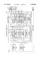
- FIG. 4shows the microcontroller of FIG. 3 incorporating the peripheral controller of FIG. 1 with an FeRAM array to allow switching of configuration data sets into the peripheral controller on the fly.
- the peripheral controller with the FeRAM arrayis an enhanced peripheral controller.
- the microcontrollergenerally contains external RAM 80', external ROM 82', microprocessor 86', low power detector 140', power on reset 142', and enhanced peripheral controller 150 made up of reconfigurable peripheral controller 152 (for example, element number 14 of FIG. 1) and FeRAM array 154.
- Reconfigurable peripheral controller 152comprises all of the logic functions and busses shown in element 14 of FIG. 1 and includes microprocessor interface 16, synchronization generator 24, clock generator 22, configurable logic array 18, communication flag port 28, communication registers 26 and programmable line drivers receivers 20.
- the microcontrollermay be on one integrated circuit.
- Reconfigurable peripheral controller 152is made from a programmable logic array (PLA) on a portion of the microcontroller chip. The logic functions of reconfigurable peripheral controller 152 are programmed into the PLA.
- FeRAM array 154contains data that defines the logic programmed into reconfigurable peripheral controller 152.
- a microprocessor 86reads the data into FeRAM array 154 and cooperates with the FeRAM to configure the data into the PLA so as to create reconfigurable peripheral controller 152.
- the reconfigurable peripheral controller 152is configured for one of the peripherals and as described with respect to FIG. 1 it may be reconfigured with another configuration data set to switch to another peripheral.
- the advantage of the FeRAMis that it operates at the speed of RAM.
- Microprocessor 86reads new configuration data sets for different peripherals into FeRAM very quickly. Then the microprocessor 86 cooperates with the FeRAM to program the configuration data set into the reconfigurable peripheral controller 152 on the fly so that the new peripheral may be used.
- FeRAMnon-volatile and reprogrammable.
- RAMhas the disadvantage that it is volatile and loses data during a power down. With FeRAM if power is shut down the microprocessor may be started up where it left off without rebooting.
- EPROMis not an option for the enhanced peripheral controller 150 because it has asymmetric read and write performance. The read may be done in nanoseconds but the write cycle may take milliseconds which is far to slow for a microprocessor and reconfigurable peripheral controller. The data to be changed in the FeRAM array could not be done on the fly. ROM may not be used for the enhanced peripheral controller 150 because ROM may only be written once and would not allow data changes to be made.
- FeRAM array 154 in new inventive peripheral controller 150complement the advantages of using FeRAM for the memory in the microcontroller as detailed previously for FIGS. 2 and 3.
- the memory in the microcontrolleris non-volatile, reprogrammable and operates with the speed of RAM.
- These same advantages with FeRAM array 154allow the multiple data set peripheral controller to work at the speed of the microprocessor and create a microprocessor that reconfigures the enhanced peripheral controller so that multiple peripherals may be switched on the fly as the microcontroller operates.
Landscapes
- Engineering & Computer Science (AREA)
- Computer Hardware Design (AREA)
- Theoretical Computer Science (AREA)
- General Engineering & Computer Science (AREA)
- Physics & Mathematics (AREA)
- General Physics & Mathematics (AREA)
- Computing Systems (AREA)
- Microelectronics & Electronic Packaging (AREA)
- Microcomputers (AREA)
Abstract
Description
Claims (15)
Priority Applications (1)
| Application Number | Priority Date | Filing Date | Title |
|---|---|---|---|
| US09/078,952US6145020A (en) | 1998-05-14 | 1998-05-14 | Microcontroller incorporating an enhanced peripheral controller for automatic updating the configuration date of multiple peripherals by using a ferroelectric memory array |
Applications Claiming Priority (1)
| Application Number | Priority Date | Filing Date | Title |
|---|---|---|---|
| US09/078,952US6145020A (en) | 1998-05-14 | 1998-05-14 | Microcontroller incorporating an enhanced peripheral controller for automatic updating the configuration date of multiple peripherals by using a ferroelectric memory array |
Publications (1)
| Publication Number | Publication Date |
|---|---|
| US6145020Atrue US6145020A (en) | 2000-11-07 |
Family
ID=22147214
Family Applications (1)
| Application Number | Title | Priority Date | Filing Date |
|---|---|---|---|
| US09/078,952Expired - LifetimeUS6145020A (en) | 1998-05-14 | 1998-05-14 | Microcontroller incorporating an enhanced peripheral controller for automatic updating the configuration date of multiple peripherals by using a ferroelectric memory array |
Country Status (1)
| Country | Link |
|---|---|
| US (1) | US6145020A (en) |
Cited By (35)
| Publication number | Priority date | Publication date | Assignee | Title |
|---|---|---|---|---|
| US20030097510A1 (en)* | 2001-11-20 | 2003-05-22 | Francis Joseph | System-On-Chip architecture that utilizes FeRAM and re-configurable hardware |
| US20030122578A1 (en)* | 2001-12-28 | 2003-07-03 | Shoichi Masui | Programmable logic device with ferroelectric configuration memories |
| US20030145245A1 (en)* | 2002-01-30 | 2003-07-31 | Kazutoshi Inoue | Microcontroller |
| US20040032282A1 (en)* | 2001-03-19 | 2004-02-19 | Altera Corporation | Programmable logic device with high speed serial interface circuitry |
| EP1220109A3 (en)* | 2000-12-26 | 2004-04-28 | Sharp Kabushiki Kaisha | Microcomputer |
| US20040115995A1 (en)* | 2002-11-25 | 2004-06-17 | Sanders Samuel Sidney | Circuit array module |
| US20040117798A1 (en)* | 2002-12-12 | 2004-06-17 | Xerox Corporation | Methods, apparatus, and program products for abstract applications/components in a ubiquitous computing environment |
| US20040139311A1 (en)* | 1999-09-29 | 2004-07-15 | Conexant Systems, Inc. | Signal processor with fast field reconfigurable datapath, data address unit, and program sequencer |
| US6946874B1 (en)* | 2003-03-11 | 2005-09-20 | Xilinx, Inc. | Structures and methods providing columns of tightly coupled processor and RAM blocks within an array of logic blocks |
| US20050237083A1 (en)* | 2003-07-31 | 2005-10-27 | Actel Corporation, A California Corporation | Programmable system on a chip |
| US7032038B1 (en)* | 2001-03-22 | 2006-04-18 | Xilinx, Inc. | Configurable peripheral devices |
| US20060119384A1 (en)* | 2004-12-02 | 2006-06-08 | Altera Corporation | Techniques for combining volatile and non-volatile programmable logic on an integrated circuit |
| US20060132250A1 (en)* | 2004-12-21 | 2006-06-22 | Actel Corporation, A California Corporation | Voltage- and temperature-compensated RC oscillator circuit |
| US20060138544A1 (en)* | 2004-12-29 | 2006-06-29 | Actel Corporation, A California Corporation | ESD protection structure for I/O pad subject to both positive and negative voltages |
| US7099189B1 (en) | 2004-10-05 | 2006-08-29 | Actel Corporation | SRAM cell controlled by non-volatile memory cell |
| US7100168B1 (en)* | 2001-06-22 | 2006-08-29 | Xilinx, Inc. | Structure and method for controlling electronic devices |
| US7119398B1 (en) | 2004-12-22 | 2006-10-10 | Actel Corporation | Power-up and power-down circuit for system-on-a-chip integrated circuit |
| US7138824B1 (en) | 2004-05-10 | 2006-11-21 | Actel Corporation | Integrated multi-function analog circuit including voltage, current, and temperature monitor and gate-driver circuit blocks |
| EP1881385A1 (en) | 2006-07-18 | 2008-01-23 | Erowa AG | System for exchanging information between a processing device and a transfer device |
| US20080048716A1 (en)* | 2003-07-31 | 2008-02-28 | Actel Corporation | Integrated circuit including programmable logic and external-device chip-enable override control |
| US20090167353A1 (en)* | 2007-12-30 | 2009-07-02 | Unity Semiconductor Corporation | State machines using resistivity-sensitive memories |
| US7685329B1 (en) | 2007-08-10 | 2010-03-23 | American Megatreads, Inc. | Detecting the presence and activity of a mass storage device |
| US7714747B2 (en) | 1998-12-11 | 2010-05-11 | Realtime Data Llc | Data compression systems and methods |
| US7734839B1 (en) | 2005-08-25 | 2010-06-08 | American Megatrends, Inc. | Method and integrated circuit for providing enclosure management services utilizing multiple interfaces and protocols |
| US7777651B2 (en) | 2000-10-03 | 2010-08-17 | Realtime Data Llc | System and method for data feed acceleration and encryption |
| US8054879B2 (en) | 2001-02-13 | 2011-11-08 | Realtime Data Llc | Bandwidth sensitive data compression and decompression |
| US8078770B1 (en)* | 2007-08-10 | 2011-12-13 | American Megatrends, Inc. | Combining multiple SGPIO streams to provide device status indicators |
| US8090936B2 (en) | 2000-02-03 | 2012-01-03 | Realtime Data, Llc | Systems and methods for accelerated loading of operating systems and application programs |
| US8260976B1 (en) | 2009-01-30 | 2012-09-04 | American Megatrends, Inc. | Multiple frequency state detection for serial I/O interfaces |
| US8275897B2 (en) | 1999-03-11 | 2012-09-25 | Realtime Data, Llc | System and methods for accelerated data storage and retrieval |
| WO2013040280A1 (en)* | 2011-09-14 | 2013-03-21 | Microchip Technology Incorporated | Peripheral trigger generator |
| US8504710B2 (en) | 1999-03-11 | 2013-08-06 | Realtime Data Llc | System and methods for accelerated data storage and retrieval |
| US8692695B2 (en) | 2000-10-03 | 2014-04-08 | Realtime Data, Llc | Methods for encoding and decoding data |
| US9143546B2 (en) | 2000-10-03 | 2015-09-22 | Realtime Data Llc | System and method for data feed acceleration and encryption |
| US10949204B2 (en)* | 2019-06-20 | 2021-03-16 | Microchip Technology Incorporated | Microcontroller with configurable logic peripheral |
Citations (25)
| Publication number | Priority date | Publication date | Assignee | Title |
|---|---|---|---|---|
| US4791603A (en)* | 1986-07-18 | 1988-12-13 | Honeywell Inc. | Dynamically reconfigurable array logic |
| US4803623A (en)* | 1986-10-31 | 1989-02-07 | Honeywell Bull Inc. | Universal peripheral controller self-configuring bootloadable ramware |
| GB2180382B (en)* | 1985-09-11 | 1989-11-22 | Pilkington Micro Electronics | Semi-conductor integrated circuits/systems |
| US4972470A (en)* | 1987-08-06 | 1990-11-20 | Steven Farago | Programmable connector |
| US5109503A (en)* | 1989-05-22 | 1992-04-28 | Ge Fanuc Automation North America, Inc. | Apparatus with reconfigurable counter includes memory for storing plurality of counter configuration files which respectively define plurality of predetermined counters |
| US5198706A (en)* | 1991-10-15 | 1993-03-30 | National Semiconductor | Ferroelectric programming cell for configurable logic |
| US5237699A (en)* | 1988-08-31 | 1993-08-17 | Dallas Semiconductor Corp. | Nonvolatile microprocessor with predetermined state on power-down |
| US5253181A (en)* | 1989-04-27 | 1993-10-12 | Kawasaki Steel Corporation | Programmable one-board computer, and methods of verification of logic circuit and alteration to actual circuit using the programmable one-board computer |
| US5379382A (en)* | 1991-04-22 | 1995-01-03 | Pilkington Micro-Electronics Limited | Uni and bi-directional signal transfer modes in peripheral controller and method of operating same |
| US5402014A (en)* | 1993-07-14 | 1995-03-28 | Waferscale Integration, Inc. | Peripheral port with volatile and non-volatile configuration |
| US5408624A (en)* | 1990-11-09 | 1995-04-18 | Ast Research, Inc. | Method and apparatus for down-loading instructions from a host computer system to a memory in a peripheral controller for execution by a core microprocessor in the peripheral controller |
| US5455923A (en)* | 1992-07-30 | 1995-10-03 | Kaplinsky; Cecil H. | Memory system for loading peripherals on power up |
| US5535406A (en)* | 1993-12-29 | 1996-07-09 | Kolchinsky; Alexander | Virtual processor module including a reconfigurable programmable matrix |
| US5572572A (en)* | 1988-05-05 | 1996-11-05 | Transaction Technology, Inc. | Computer and telephone apparatus with user friendly interface and enhanced integrity features |
| US5574388A (en)* | 1995-10-13 | 1996-11-12 | Mentor Graphics Corporation | Emulation system having a scalable multi-level multi-stage programmable interconnect network |
| US5590305A (en)* | 1994-03-28 | 1996-12-31 | Altera Corporation | Programming circuits and techniques for programming logic |
| US5684980A (en)* | 1992-07-29 | 1997-11-04 | Virtual Computer Corporation | FPGA virtual computer for executing a sequence of program instructions by successively reconfiguring a group of FPGA in response to those instructions |
| US5758127A (en)* | 1994-04-15 | 1998-05-26 | Vlsi Technology, Inc. | Method and apparatus for providing a plurality of protocol serial communications |
| US5799203A (en)* | 1996-05-17 | 1998-08-25 | Advanced Micro Devices, Inc. | System for receiving peripheral device capability information and selectively disabling corresponding processing unit function when the device failing to support such function |
| US5812867A (en)* | 1993-01-13 | 1998-09-22 | Sgs-Thomson Microelectronics, S.A. | Integrated circuit comprising a microprocessor, a memory and internal configurable peripherals |
| US5862375A (en)* | 1990-08-31 | 1999-01-19 | Advanced Micro Devices, Inc. | System for effecting communications between a computing device and a plurality of peripheral devices |
| US5890199A (en)* | 1996-10-21 | 1999-03-30 | Ramtron International Corporation | Data processor incorporating a ferroelectric memory array selectably configurable as read/write and read only memory |
| US5892942A (en)* | 1995-08-01 | 1999-04-06 | Nippondenso Co., Ltd. | Control system with microcomputer and associated electrically reconfigurable logic circuit |
| US5896338A (en)* | 1997-04-11 | 1999-04-20 | Intel Corporation | Input/output power supply detection scheme for flash memory |
| US5936879A (en)* | 1996-07-13 | 1999-08-10 | Mitel Semiconductor Limited | Programmable logic arrays |
- 1998
- 1998-05-14USUS09/078,952patent/US6145020A/ennot_activeExpired - Lifetime
Patent Citations (25)
| Publication number | Priority date | Publication date | Assignee | Title |
|---|---|---|---|---|
| GB2180382B (en)* | 1985-09-11 | 1989-11-22 | Pilkington Micro Electronics | Semi-conductor integrated circuits/systems |
| US4791603A (en)* | 1986-07-18 | 1988-12-13 | Honeywell Inc. | Dynamically reconfigurable array logic |
| US4803623A (en)* | 1986-10-31 | 1989-02-07 | Honeywell Bull Inc. | Universal peripheral controller self-configuring bootloadable ramware |
| US4972470A (en)* | 1987-08-06 | 1990-11-20 | Steven Farago | Programmable connector |
| US5572572A (en)* | 1988-05-05 | 1996-11-05 | Transaction Technology, Inc. | Computer and telephone apparatus with user friendly interface and enhanced integrity features |
| US5237699A (en)* | 1988-08-31 | 1993-08-17 | Dallas Semiconductor Corp. | Nonvolatile microprocessor with predetermined state on power-down |
| US5253181A (en)* | 1989-04-27 | 1993-10-12 | Kawasaki Steel Corporation | Programmable one-board computer, and methods of verification of logic circuit and alteration to actual circuit using the programmable one-board computer |
| US5109503A (en)* | 1989-05-22 | 1992-04-28 | Ge Fanuc Automation North America, Inc. | Apparatus with reconfigurable counter includes memory for storing plurality of counter configuration files which respectively define plurality of predetermined counters |
| US5862375A (en)* | 1990-08-31 | 1999-01-19 | Advanced Micro Devices, Inc. | System for effecting communications between a computing device and a plurality of peripheral devices |
| US5408624A (en)* | 1990-11-09 | 1995-04-18 | Ast Research, Inc. | Method and apparatus for down-loading instructions from a host computer system to a memory in a peripheral controller for execution by a core microprocessor in the peripheral controller |
| US5379382A (en)* | 1991-04-22 | 1995-01-03 | Pilkington Micro-Electronics Limited | Uni and bi-directional signal transfer modes in peripheral controller and method of operating same |
| US5198706A (en)* | 1991-10-15 | 1993-03-30 | National Semiconductor | Ferroelectric programming cell for configurable logic |
| US5684980A (en)* | 1992-07-29 | 1997-11-04 | Virtual Computer Corporation | FPGA virtual computer for executing a sequence of program instructions by successively reconfiguring a group of FPGA in response to those instructions |
| US5455923A (en)* | 1992-07-30 | 1995-10-03 | Kaplinsky; Cecil H. | Memory system for loading peripherals on power up |
| US5812867A (en)* | 1993-01-13 | 1998-09-22 | Sgs-Thomson Microelectronics, S.A. | Integrated circuit comprising a microprocessor, a memory and internal configurable peripherals |
| US5402014A (en)* | 1993-07-14 | 1995-03-28 | Waferscale Integration, Inc. | Peripheral port with volatile and non-volatile configuration |
| US5535406A (en)* | 1993-12-29 | 1996-07-09 | Kolchinsky; Alexander | Virtual processor module including a reconfigurable programmable matrix |
| US5590305A (en)* | 1994-03-28 | 1996-12-31 | Altera Corporation | Programming circuits and techniques for programming logic |
| US5758127A (en)* | 1994-04-15 | 1998-05-26 | Vlsi Technology, Inc. | Method and apparatus for providing a plurality of protocol serial communications |
| US5892942A (en)* | 1995-08-01 | 1999-04-06 | Nippondenso Co., Ltd. | Control system with microcomputer and associated electrically reconfigurable logic circuit |
| US5574388A (en)* | 1995-10-13 | 1996-11-12 | Mentor Graphics Corporation | Emulation system having a scalable multi-level multi-stage programmable interconnect network |
| US5799203A (en)* | 1996-05-17 | 1998-08-25 | Advanced Micro Devices, Inc. | System for receiving peripheral device capability information and selectively disabling corresponding processing unit function when the device failing to support such function |
| US5936879A (en)* | 1996-07-13 | 1999-08-10 | Mitel Semiconductor Limited | Programmable logic arrays |
| US5890199A (en)* | 1996-10-21 | 1999-03-30 | Ramtron International Corporation | Data processor incorporating a ferroelectric memory array selectably configurable as read/write and read only memory |
| US5896338A (en)* | 1997-04-11 | 1999-04-20 | Intel Corporation | Input/output power supply detection scheme for flash memory |
Non-Patent Citations (2)
| Title |
|---|
| Mead and Conway, Introduction to VLSI Systems , pp. 237 242.* |
| Mead and Conway, Introduction to VLSI Systems, pp. 237-242. |
Cited By (134)
| Publication number | Priority date | Publication date | Assignee | Title |
|---|---|---|---|---|
| US8933825B2 (en) | 1998-12-11 | 2015-01-13 | Realtime Data Llc | Data compression systems and methods |
| US9054728B2 (en) | 1998-12-11 | 2015-06-09 | Realtime Data, Llc | Data compression systems and methods |
| US10033405B2 (en) | 1998-12-11 | 2018-07-24 | Realtime Data Llc | Data compression systems and method |
| US8717203B2 (en) | 1998-12-11 | 2014-05-06 | Realtime Data, Llc | Data compression systems and methods |
| US7714747B2 (en) | 1998-12-11 | 2010-05-11 | Realtime Data Llc | Data compression systems and methods |
| US8502707B2 (en) | 1998-12-11 | 2013-08-06 | Realtime Data, Llc | Data compression systems and methods |
| US8643513B2 (en) | 1998-12-11 | 2014-02-04 | Realtime Data Llc | Data compression systems and methods |
| US8756332B2 (en) | 1999-03-11 | 2014-06-17 | Realtime Data Llc | System and methods for accelerated data storage and retrieval |
| US8719438B2 (en) | 1999-03-11 | 2014-05-06 | Realtime Data Llc | System and methods for accelerated data storage and retrieval |
| US8275897B2 (en) | 1999-03-11 | 2012-09-25 | Realtime Data, Llc | System and methods for accelerated data storage and retrieval |
| US8504710B2 (en) | 1999-03-11 | 2013-08-06 | Realtime Data Llc | System and methods for accelerated data storage and retrieval |
| US10019458B2 (en) | 1999-03-11 | 2018-07-10 | Realtime Data Llc | System and methods for accelerated data storage and retrieval |
| US9116908B2 (en) | 1999-03-11 | 2015-08-25 | Realtime Data Llc | System and methods for accelerated data storage and retrieval |
| US20040139311A1 (en)* | 1999-09-29 | 2004-07-15 | Conexant Systems, Inc. | Signal processor with fast field reconfigurable datapath, data address unit, and program sequencer |
| US20050066152A1 (en)* | 1999-09-29 | 2005-03-24 | Kenneth Garey | Method and apparatus for processing data in a reconfigurable manner |
| US8880862B2 (en) | 2000-02-03 | 2014-11-04 | Realtime Data, Llc | Systems and methods for accelerated loading of operating systems and application programs |
| US9792128B2 (en) | 2000-02-03 | 2017-10-17 | Realtime Data, Llc | System and method for electrical boot-device-reset signals |
| US8090936B2 (en) | 2000-02-03 | 2012-01-03 | Realtime Data, Llc | Systems and methods for accelerated loading of operating systems and application programs |
| US8112619B2 (en) | 2000-02-03 | 2012-02-07 | Realtime Data Llc | Systems and methods for accelerated loading of operating systems and application programs |
| US8742958B2 (en) | 2000-10-03 | 2014-06-03 | Realtime Data Llc | Methods for encoding and decoding data |
| US9667751B2 (en) | 2000-10-03 | 2017-05-30 | Realtime Data, Llc | Data feed acceleration |
| US10419021B2 (en) | 2000-10-03 | 2019-09-17 | Realtime Data, Llc | Systems and methods of data compression |
| US9141992B2 (en) | 2000-10-03 | 2015-09-22 | Realtime Data Llc | Data feed acceleration |
| US10284225B2 (en) | 2000-10-03 | 2019-05-07 | Realtime Data, Llc | Systems and methods for data compression |
| US9143546B2 (en) | 2000-10-03 | 2015-09-22 | Realtime Data Llc | System and method for data feed acceleration and encryption |
| US9967368B2 (en) | 2000-10-03 | 2018-05-08 | Realtime Data Llc | Systems and methods for data block decompression |
| US9859919B2 (en) | 2000-10-03 | 2018-01-02 | Realtime Data Llc | System and method for data compression |
| US7777651B2 (en) | 2000-10-03 | 2010-08-17 | Realtime Data Llc | System and method for data feed acceleration and encryption |
| US8723701B2 (en) | 2000-10-03 | 2014-05-13 | Realtime Data Llc | Methods for encoding and decoding data |
| US8717204B2 (en) | 2000-10-03 | 2014-05-06 | Realtime Data Llc | Methods for encoding and decoding data |
| US8692695B2 (en) | 2000-10-03 | 2014-04-08 | Realtime Data, Llc | Methods for encoding and decoding data |
| US6826633B2 (en) | 2000-12-26 | 2004-11-30 | Sharp Kabushiki Kaisha | Microcomputer incorporating peripheral circuits |
| EP1220109A3 (en)* | 2000-12-26 | 2004-04-28 | Sharp Kabushiki Kaisha | Microcomputer |
| US8054879B2 (en) | 2001-02-13 | 2011-11-08 | Realtime Data Llc | Bandwidth sensitive data compression and decompression |
| US8073047B2 (en) | 2001-02-13 | 2011-12-06 | Realtime Data, Llc | Bandwidth sensitive data compression and decompression |
| US8867610B2 (en) | 2001-02-13 | 2014-10-21 | Realtime Data Llc | System and methods for video and audio data distribution |
| US8934535B2 (en) | 2001-02-13 | 2015-01-13 | Realtime Data Llc | Systems and methods for video and audio data storage and distribution |
| US10212417B2 (en) | 2001-02-13 | 2019-02-19 | Realtime Adaptive Streaming Llc | Asymmetric data decompression systems |
| US8929442B2 (en) | 2001-02-13 | 2015-01-06 | Realtime Data, Llc | System and methods for video and audio data distribution |
| US8553759B2 (en) | 2001-02-13 | 2013-10-08 | Realtime Data, Llc | Bandwidth sensitive data compression and decompression |
| US9769477B2 (en) | 2001-02-13 | 2017-09-19 | Realtime Adaptive Streaming, LLC | Video data compression systems |
| US9762907B2 (en) | 2001-02-13 | 2017-09-12 | Realtime Adaptive Streaming, LLC | System and methods for video and audio data distribution |
| US20060095605A1 (en)* | 2001-03-19 | 2006-05-04 | Lee Chong H | Programmable logic device with high speed serial interface circuitry |
| US20040032282A1 (en)* | 2001-03-19 | 2004-02-19 | Altera Corporation | Programmable logic device with high speed serial interface circuitry |
| US7002368B2 (en) | 2001-03-19 | 2006-02-21 | Altera Corporation | Programmable logic device with high speed serial interface circuitry |
| US20050212556A1 (en)* | 2001-03-19 | 2005-09-29 | Altera Corporation | Programmable logic device with high speed serial interface circuitry |
| US7088133B2 (en) | 2001-03-19 | 2006-08-08 | Altera Corporation | Programmable logic device with high speed serial interface circuitry |
| US7032038B1 (en)* | 2001-03-22 | 2006-04-18 | Xilinx, Inc. | Configurable peripheral devices |
| US7100168B1 (en)* | 2001-06-22 | 2006-08-29 | Xilinx, Inc. | Structure and method for controlling electronic devices |
| US20030097510A1 (en)* | 2001-11-20 | 2003-05-22 | Francis Joseph | System-On-Chip architecture that utilizes FeRAM and re-configurable hardware |
| EP1313028A3 (en)* | 2001-11-20 | 2004-09-01 | Agilent Technologies, Inc. | System-on-chip architecture that utilizes feram and re-configurable hardware |
| US6924663B2 (en)* | 2001-12-28 | 2005-08-02 | Fujitsu Limited | Programmable logic device with ferroelectric configuration memories |
| US20030122578A1 (en)* | 2001-12-28 | 2003-07-03 | Shoichi Masui | Programmable logic device with ferroelectric configuration memories |
| US7058842B2 (en)* | 2002-01-30 | 2006-06-06 | Oki Electric Industry Co., Ltd. | Microcontroller with multiple function blocks and clock signal control |
| US20030145245A1 (en)* | 2002-01-30 | 2003-07-31 | Kazutoshi Inoue | Microcontroller |
| US20040115995A1 (en)* | 2002-11-25 | 2004-06-17 | Sanders Samuel Sidney | Circuit array module |
| US20040117798A1 (en)* | 2002-12-12 | 2004-06-17 | Xerox Corporation | Methods, apparatus, and program products for abstract applications/components in a ubiquitous computing environment |
| US7620737B2 (en)* | 2002-12-12 | 2009-11-17 | Xerox Corporation | Methods, apparatus, and program products for abstract applications/components in a ubiquitous computing environment |
| US7181718B1 (en) | 2003-03-11 | 2007-02-20 | Xilinx, Inc. | Structures and methods providing columns of tightly coupled processor and RAM blocks within an array of logic blocks |
| US6946874B1 (en)* | 2003-03-11 | 2005-09-20 | Xilinx, Inc. | Structures and methods providing columns of tightly coupled processor and RAM blocks within an array of logic blocks |
| US7352206B1 (en) | 2003-07-31 | 2008-04-01 | Actel Corporation | Integrated circuit device having state-saving and initialization feature |
| US20080272803A1 (en)* | 2003-07-31 | 2008-11-06 | Actel Corporation | System-on-a-chip integrated circuit including dual-function analog and digital inputs |
| US7446560B2 (en) | 2003-07-31 | 2008-11-04 | Actel Corporation | Programmable system on a chip for temperature monitoring and control |
| US20080309393A1 (en)* | 2003-07-31 | 2008-12-18 | Actel Corporation | Clock-generator architecture for a programmable-logic-based system on a chip |
| US7487376B2 (en) | 2003-07-31 | 2009-02-03 | Actel Corporation | Programmable system on a chip |
| US7492183B2 (en) | 2003-07-31 | 2009-02-17 | Actel Corporation | Programmable system on a chip for power-supply voltage and current monitoring and control |
| US7493506B2 (en) | 2003-07-31 | 2009-02-17 | Actel Corporation | Programmable system on a chip for power-supply voltage and current monitoring and control |
| US7521960B2 (en) | 2003-07-31 | 2009-04-21 | Actel Corporation | Integrated circuit including programmable logic and external-device chip-enable override control |
| US20090128186A1 (en)* | 2003-07-31 | 2009-05-21 | Actel Corporation | Programmable system on a chip for power-supply voltage and current monitoring and control |
| US20080224731A1 (en)* | 2003-07-31 | 2008-09-18 | Actel Corporation | Non-volatile memory architecture for programmable-logic-based system on a chip |
| US7423451B2 (en) | 2003-07-31 | 2008-09-09 | Actel Corporation | System-on-a-chip integrated circuit including dual-function analog and digital inputs |
| US7560952B2 (en) | 2003-07-31 | 2009-07-14 | Actel Corporation | Integrated circuit device having state-saving and initialization feature |
| US7560954B2 (en) | 2003-07-31 | 2009-07-14 | Actel Corporation | Programmable system on a chip for temperature monitoring and control |
| US7579895B2 (en) | 2003-07-31 | 2009-08-25 | Actel Corporation | Clock-generator architecture for a programmable-logic-based system on a chip |
| US7603578B2 (en) | 2003-07-31 | 2009-10-13 | Actel Corporation | Programmable system on a chip for power-supply voltage and current monitoring and control |
| US7613943B2 (en) | 2003-07-31 | 2009-11-03 | Actel Corporation | Programmable system on a chip |
| US7616026B2 (en) | 2003-07-31 | 2009-11-10 | Actel Corporation | System-on-a-chip integrated circuit including dual-function analog and digital inputs |
| US20080122481A1 (en)* | 2003-07-31 | 2008-05-29 | Actel Corporation | Programmable system on a chip |
| US20090292937A1 (en)* | 2003-07-31 | 2009-11-26 | Actel Corporation | Programmable system on a chip |
| US7675320B2 (en) | 2003-07-31 | 2010-03-09 | Actel Corporation | Non-volatile memory architecture for programmable-logic-based system on a chip |
| US20080122484A1 (en)* | 2003-07-31 | 2008-05-29 | Actel Corporation | Integrated circuit device having state-saving and intitalization feature |
| US7365565B2 (en) | 2003-07-31 | 2008-04-29 | Actel Corporation | Programmable system on a chip for power-supply voltage and current monitoring and control |
| US7362131B2 (en) | 2003-07-31 | 2008-04-22 | Actel Corporation | Integrated circuit including programmable logic and external-device chip-enable override control |
| US20080061822A1 (en)* | 2003-07-31 | 2008-03-13 | Actel Corporation | Programmable system on a chip for power-supply voltage and current monitoring and control |
| US20080048715A1 (en)* | 2003-07-31 | 2008-02-28 | Actel Corporation, A California Corporation | Programmable system on a chip for power-supply voltage and current monitoring and control |
| US20080048717A1 (en)* | 2003-07-31 | 2008-02-28 | Actel Corporation | Programmable system on a chip |
| US20080048716A1 (en)* | 2003-07-31 | 2008-02-28 | Actel Corporation | Integrated circuit including programmable logic and external-device chip-enable override control |
| US7256610B1 (en) | 2003-07-31 | 2007-08-14 | Actel Corporation | Programmable system on a chip for temperature monitoring and control |
| US7937601B2 (en) | 2003-07-31 | 2011-05-03 | Actel Corporation | Programmable system on a chip |
| US20070046325A1 (en)* | 2003-07-31 | 2007-03-01 | Actel Corporation | System-on-a-chip integrated circuit including dual-function analog and digital inputs |
| US7170315B2 (en) | 2003-07-31 | 2007-01-30 | Actel Corporation | Programmable system on a chip |
| US7129746B1 (en) | 2003-07-31 | 2006-10-31 | Actel Corporation | System-on-a-chip integrated circuit including dual-function analog and digital inputs |
| US7102391B1 (en) | 2003-07-31 | 2006-09-05 | Actel Corporation | Clock-generator architecture for a programmable-logic-based system on a chip |
| US7102384B1 (en) | 2003-07-31 | 2006-09-05 | Actel Corporation | Non-volatile memory architecture for programmable-logic-based system on a chip |
| US20060181305A1 (en)* | 2003-07-31 | 2006-08-17 | Actel Corporation | Integrated circuit including programmable logic and external-device chip-enable override control |
| US20060119385A1 (en)* | 2003-07-31 | 2006-06-08 | Actel Corporation, A California Corporation | Programmable system on a chip for power-supply voltage and current monitoring and control |
| US7034569B1 (en) | 2003-07-31 | 2006-04-25 | Actel Corporation | Programmable system on a chip for power-supply voltage and current monitoring and control |
| US7030649B1 (en) | 2003-07-31 | 2006-04-18 | Actel Corporation | Integrated circuit including programmable logic and external-device chip-enable override control |
| US20050237083A1 (en)* | 2003-07-31 | 2005-10-27 | Actel Corporation, A California Corporation | Programmable system on a chip |
| US7138824B1 (en) | 2004-05-10 | 2006-11-21 | Actel Corporation | Integrated multi-function analog circuit including voltage, current, and temperature monitor and gate-driver circuit blocks |
| US20080094101A1 (en)* | 2004-05-10 | 2008-04-24 | Actel Corporation | Programmable system on a chip for power-supply voltage and current monitoring and control |
| US7414427B1 (en) | 2004-05-10 | 2008-08-19 | Actel Corporation | Integrated multi-function analog circuit including voltage, current, and temperature monitor and gate-driver circuit blocks |
| US7421605B2 (en) | 2004-05-10 | 2008-09-02 | Actel Corporation | Programmable system on a chip for power-supply voltage and current monitoring and control |
| US20080265935A1 (en)* | 2004-05-10 | 2008-10-30 | Acetel Corporation | Integrated multi-function analog circuit including voltage, current, and temperature monitor and gate-driver circuit blocks |
| US7558112B2 (en) | 2004-10-05 | 2009-07-07 | Actel Corporation | SRAM cell controlled by flash memory cell |
| US7099189B1 (en) | 2004-10-05 | 2006-08-29 | Actel Corporation | SRAM cell controlled by non-volatile memory cell |
| US20080266955A1 (en)* | 2004-10-05 | 2008-10-30 | Actel Corporation | Sram cell controlled by flash memory cell |
| US20060119384A1 (en)* | 2004-12-02 | 2006-06-08 | Altera Corporation | Techniques for combining volatile and non-volatile programmable logic on an integrated circuit |
| US7242218B2 (en)* | 2004-12-02 | 2007-07-10 | Altera Corporation | Techniques for combining volatile and non-volatile programmable logic on an integrated circuit |
| US20080284532A1 (en)* | 2004-12-21 | 2008-11-20 | Actel Corporation | Voltage- and temperature-compensated rc oscillator circuit |
| US20060132250A1 (en)* | 2004-12-21 | 2006-06-22 | Actel Corporation, A California Corporation | Voltage- and temperature-compensated RC oscillator circuit |
| US7116181B2 (en) | 2004-12-21 | 2006-10-03 | Actel Corporation | Voltage- and temperature-compensated RC oscillator circuit |
| US20060284666A1 (en)* | 2004-12-21 | 2006-12-21 | Actel Corporation, A California Corporation | Voltage-and temperature-compensated rc oscillator circuit |
| US7439818B2 (en) | 2004-12-21 | 2008-10-21 | Actel Corporation | Voltage-and temperature-compensated RC oscillator circuit |
| US7911226B2 (en) | 2004-12-22 | 2011-03-22 | Actel Corporation | Power-up and power-down circuit for system-on-a-chip integrated circuit |
| US7119398B1 (en) | 2004-12-22 | 2006-10-10 | Actel Corporation | Power-up and power-down circuit for system-on-a-chip integrated circuit |
| US20060284324A1 (en)* | 2004-12-22 | 2006-12-21 | Actel Corporation | Power-up and power-down circuit for system-on-a-chip integrated circuit |
| US20060138544A1 (en)* | 2004-12-29 | 2006-06-29 | Actel Corporation, A California Corporation | ESD protection structure for I/O pad subject to both positive and negative voltages |
| US8051216B2 (en) | 2005-08-25 | 2011-11-01 | American Megatrends, Inc. | Method and integrated circuit for providing enclosure management services utilizing multiple interfaces and protocols |
| US7908407B1 (en) | 2005-08-25 | 2011-03-15 | American Megatrends, Inc. | Method, computer-readable storage media, and integrated circuit for providing enclosure management services utilizing multiple interfaces and protocols |
| US20110125941A1 (en)* | 2005-08-25 | 2011-05-26 | American Megatrends, Inc. | Method and integrated circuit for providing enclosure management services utilizing multiple interfaces and protocols |
| US7734839B1 (en) | 2005-08-25 | 2010-06-08 | American Megatrends, Inc. | Method and integrated circuit for providing enclosure management services utilizing multiple interfaces and protocols |
| EP1881385A1 (en) | 2006-07-18 | 2008-01-23 | Erowa AG | System for exchanging information between a processing device and a transfer device |
| US8161203B1 (en) | 2007-08-10 | 2012-04-17 | American Megatrends, Inc. | Detecting the presence and activity of a mass storage device |
| US8078770B1 (en)* | 2007-08-10 | 2011-12-13 | American Megatrends, Inc. | Combining multiple SGPIO streams to provide device status indicators |
| US7685329B1 (en) | 2007-08-10 | 2010-03-23 | American Megatreads, Inc. | Detecting the presence and activity of a mass storage device |
| US7834660B2 (en)* | 2007-12-30 | 2010-11-16 | Unity Semiconductor Corporation | State machines using resistivity-sensitive memories |
| US20090167353A1 (en)* | 2007-12-30 | 2009-07-02 | Unity Semiconductor Corporation | State machines using resistivity-sensitive memories |
| US20110062989A1 (en)* | 2007-12-30 | 2011-03-17 | Unity Semiconductor Corporation | State machines using non-volatile re-writeable two-terminal resistivity-sensitive memories |
| US7999571B2 (en)* | 2007-12-30 | 2011-08-16 | Unity Semiconductor Corporation | State machines using non-volatile re-writeable two-terminal resistivity-sensitive memories |
| US8260976B1 (en) | 2009-01-30 | 2012-09-04 | American Megatrends, Inc. | Multiple frequency state detection for serial I/O interfaces |
| WO2013040280A1 (en)* | 2011-09-14 | 2013-03-21 | Microchip Technology Incorporated | Peripheral trigger generator |
| US8856406B2 (en) | 2011-09-14 | 2014-10-07 | Microchip Technology Incorporated | Peripheral trigger generator |
| US10949204B2 (en)* | 2019-06-20 | 2021-03-16 | Microchip Technology Incorporated | Microcontroller with configurable logic peripheral |
Similar Documents
| Publication | Publication Date | Title |
|---|---|---|
| US6145020A (en) | Microcontroller incorporating an enhanced peripheral controller for automatic updating the configuration date of multiple peripherals by using a ferroelectric memory array | |
| KR100363983B1 (en) | Semiconductor integrated circuit | |
| EP1652058B1 (en) | Switch/network adapter port incorporating selectively accessible shared memory resources | |
| US5097154A (en) | Latched multiplexer for stabilizing the switch crystal to ring oscillator at power-down | |
| US5860021A (en) | Single chip microcontroller having down-loadable memory organization supporting "shadow" personality, optimized for bi-directional data transfers over a communication channel | |
| CN1936876B (en) | Data processing system and data processor | |
| CN100418079C (en) | serial peripheral interface memory element with parallel acceleration mode | |
| EP1226505B1 (en) | Generic serial port architecture and system | |
| US8756360B1 (en) | PCI-E compatible chassis having multi-host capability | |
| US20030236934A1 (en) | Memory drive having multi-connector and method of controlling the same | |
| US7617383B2 (en) | Circular register arrays of a computer | |
| NO176079B (en) | Integrated circuit board | |
| US6157979A (en) | Programmable controlling device with non-volatile ferroelectric state-machines for restarting processor when power is restored with execution states retained in said non-volatile state-machines on power down | |
| US6216191B1 (en) | Field programmable gate array having a dedicated processor interface | |
| WO1989002128A1 (en) | Microcomputer with on-board chip selects and programmable bus stretching | |
| EP0843893B1 (en) | A microcontroller having an n-bit data bus width with less than n i/o pins | |
| EP1423775A2 (en) | Microprocessor with multiple low power modes and emulation apparatus for said microprocessor | |
| JP2004192488A (en) | Data processor and memory card | |
| US4460972A (en) | Single chip microcomputer selectively operable in response to instructions stored on the computer chip or in response to instructions stored external to the chip | |
| CN1333357C (en) | In-circuit configuration structure with non-volatile configuration storage | |
| EP4266185A1 (en) | Microcontroller chip containing multi-protocol communication interface peripheral and operation method therefor | |
| EP1229549A1 (en) | Asynchronous flash-eeprom behaving like a synchronous ram/rom | |
| EP0322856B1 (en) | Microcomputer | |
| MXPA02009213A (en) | A communication interface system, method and apparatus. | |
| US20040122984A1 (en) | Data processor and data table update method |
Legal Events
| Date | Code | Title | Description |
|---|---|---|---|
| AS | Assignment | Owner name:ADVANCED TECHNOLOGY MATERIALS, INC., CONNECTICUT Free format text:ASSIGNMENT OF ASSIGNORS INTEREST;ASSIGNOR:BARNETT, PHILIP C.;REEL/FRAME:009173/0004 Effective date:19980505 | |
| STCF | Information on status: patent grant | Free format text:PATENTED CASE | |
| FEPP | Fee payment procedure | Free format text:PAT HOLDER NO LONGER CLAIMS SMALL ENTITY STATUS, ENTITY STATUS SET TO UNDISCOUNTED (ORIGINAL EVENT CODE: STOL); ENTITY STATUS OF PATENT OWNER: LARGE ENTITY | |
| FPAY | Fee payment | Year of fee payment:4 | |
| AS | Assignment | Owner name:EMOSYN AMERICA, INC., CALIFORNIA Free format text:ASSIGNMENT OF ASSIGNORS INTEREST;ASSIGNOR:ADVANCED TECHNOLOGY MATERIALS, INC.;REEL/FRAME:015503/0023 Effective date:20040910 | |
| AS | Assignment | Owner name:SILICON STORAGE TECHNOLOGY, INC., CALIFORNIA Free format text:ASSIGNMENT OF ASSIGNORS INTEREST;ASSIGNOR:EMOSYN AMERICA, INC.;REEL/FRAME:016793/0321 Effective date:20051110 | |
| FPAY | Fee payment | Year of fee payment:8 | |
| FPAY | Fee payment | Year of fee payment:12 | |
| AS | Assignment | Owner name:JPMORGAN CHASE BANK, N.A., AS ADMINISTRATIVE AGENT, ILLINOIS Free format text:SECURITY INTEREST;ASSIGNOR:SILICON STORAGE TECHNOLOGY, INC.;REEL/FRAME:041675/0316 Effective date:20170208 Owner name:JPMORGAN CHASE BANK, N.A., AS ADMINISTRATIVE AGENT Free format text:SECURITY INTEREST;ASSIGNOR:SILICON STORAGE TECHNOLOGY, INC.;REEL/FRAME:041675/0316 Effective date:20170208 | |
| AS | Assignment | Owner name:JPMORGAN CHASE BANK, N.A., AS ADMINISTRATIVE AGENT, ILLINOIS Free format text:SECURITY INTEREST;ASSIGNORS:MICROCHIP TECHNOLOGY INCORPORATED;SILICON STORAGE TECHNOLOGY, INC.;ATMEL CORPORATION;AND OTHERS;REEL/FRAME:046426/0001 Effective date:20180529 Owner name:JPMORGAN CHASE BANK, N.A., AS ADMINISTRATIVE AGENT Free format text:SECURITY INTEREST;ASSIGNORS:MICROCHIP TECHNOLOGY INCORPORATED;SILICON STORAGE TECHNOLOGY, INC.;ATMEL CORPORATION;AND OTHERS;REEL/FRAME:046426/0001 Effective date:20180529 | |
| AS | Assignment | Owner name:WELLS FARGO BANK, NATIONAL ASSOCIATION, AS NOTES COLLATERAL AGENT, CALIFORNIA Free format text:SECURITY INTEREST;ASSIGNORS:MICROCHIP TECHNOLOGY INCORPORATED;SILICON STORAGE TECHNOLOGY, INC.;ATMEL CORPORATION;AND OTHERS;REEL/FRAME:047103/0206 Effective date:20180914 Owner name:WELLS FARGO BANK, NATIONAL ASSOCIATION, AS NOTES C Free format text:SECURITY INTEREST;ASSIGNORS:MICROCHIP TECHNOLOGY INCORPORATED;SILICON STORAGE TECHNOLOGY, INC.;ATMEL CORPORATION;AND OTHERS;REEL/FRAME:047103/0206 Effective date:20180914 | |
| AS | Assignment | Owner name:MICROSEMI STORAGE SOLUTIONS, INC., ARIZONA Free format text:RELEASE BY SECURED PARTY;ASSIGNOR:JPMORGAN CHASE BANK, N.A., AS ADMINISTRATIVE AGENT;REEL/FRAME:059333/0222 Effective date:20220218 Owner name:MICROSEMI CORPORATION, ARIZONA Free format text:RELEASE BY SECURED PARTY;ASSIGNOR:JPMORGAN CHASE BANK, N.A., AS ADMINISTRATIVE AGENT;REEL/FRAME:059333/0222 Effective date:20220218 Owner name:ATMEL CORPORATION, ARIZONA Free format text:RELEASE BY SECURED PARTY;ASSIGNOR:JPMORGAN CHASE BANK, N.A., AS ADMINISTRATIVE AGENT;REEL/FRAME:059333/0222 Effective date:20220218 Owner name:SILICON STORAGE TECHNOLOGY, INC., ARIZONA Free format text:RELEASE BY SECURED PARTY;ASSIGNOR:JPMORGAN CHASE BANK, N.A., AS ADMINISTRATIVE AGENT;REEL/FRAME:059333/0222 Effective date:20220218 Owner name:MICROCHIP TECHNOLOGY INCORPORATED, ARIZONA Free format text:RELEASE BY SECURED PARTY;ASSIGNOR:JPMORGAN CHASE BANK, N.A., AS ADMINISTRATIVE AGENT;REEL/FRAME:059333/0222 Effective date:20220218 | |
| AS | Assignment | Owner name:SILICON STORAGE TECHNOLOGY, INC., ARIZONA Free format text:RELEASE BY SECURED PARTY;ASSIGNOR:JPMORGAN CHASE BANK, N.A., AS ADMINISTRATIVE AGENT;REEL/FRAME:059687/0344 Effective date:20220218 | |
| AS | Assignment | Owner name:MICROSEMI STORAGE SOLUTIONS, INC., ARIZONA Free format text:RELEASE BY SECURED PARTY;ASSIGNOR:WELLS FARGO BANK, NATIONAL ASSOCIATION, AS NOTES COLLATERAL AGENT;REEL/FRAME:059358/0001 Effective date:20220228 Owner name:MICROSEMI CORPORATION, ARIZONA Free format text:RELEASE BY SECURED PARTY;ASSIGNOR:WELLS FARGO BANK, NATIONAL ASSOCIATION, AS NOTES COLLATERAL AGENT;REEL/FRAME:059358/0001 Effective date:20220228 Owner name:ATMEL CORPORATION, ARIZONA Free format text:RELEASE BY SECURED PARTY;ASSIGNOR:WELLS FARGO BANK, NATIONAL ASSOCIATION, AS NOTES COLLATERAL AGENT;REEL/FRAME:059358/0001 Effective date:20220228 Owner name:SILICON STORAGE TECHNOLOGY, INC., ARIZONA Free format text:RELEASE BY SECURED PARTY;ASSIGNOR:WELLS FARGO BANK, NATIONAL ASSOCIATION, AS NOTES COLLATERAL AGENT;REEL/FRAME:059358/0001 Effective date:20220228 Owner name:MICROCHIP TECHNOLOGY INCORPORATED, ARIZONA Free format text:RELEASE BY SECURED PARTY;ASSIGNOR:WELLS FARGO BANK, NATIONAL ASSOCIATION, AS NOTES COLLATERAL AGENT;REEL/FRAME:059358/0001 Effective date:20220228 |