US6144708A - Phase-locked loop circuit with equalizer and phase locking method - Google Patents
Phase-locked loop circuit with equalizer and phase locking methodDownload PDFInfo
- Publication number
- US6144708A US6144708AUS09/083,342US8334298AUS6144708AUS 6144708 AUS6144708 AUS 6144708AUS 8334298 AUS8334298 AUS 8334298AUS 6144708 AUS6144708 AUS 6144708A
- Authority
- US
- United States
- Prior art keywords
- phase
- equalizer
- amplitude value
- locked loop
- received signal
- Prior art date
- Legal status (The legal status is an assumption and is not a legal conclusion. Google has not performed a legal analysis and makes no representation as to the accuracy of the status listed.)
- Expired - Lifetime
Links
- 238000000034methodMethods0.000titleclaimsdescription9
- 230000005540biological transmissionEffects0.000claimsabstractdescription29
- 230000003111delayed effectEffects0.000claimsdescription4
- 230000010354integrationEffects0.000abstractdescription6
- 238000005562fadingMethods0.000abstractdescription5
- 238000010586diagramMethods0.000description8
- 238000006243chemical reactionMethods0.000description1
- 239000013078crystalSubstances0.000description1
- 230000000694effectsEffects0.000description1
- 230000010355oscillationEffects0.000description1
- 230000010363phase shiftEffects0.000description1
- 238000001228spectrumMethods0.000description1
Images

Classifications
- H—ELECTRICITY
- H04—ELECTRIC COMMUNICATION TECHNIQUE
- H04L—TRANSMISSION OF DIGITAL INFORMATION, e.g. TELEGRAPHIC COMMUNICATION
- H04L27/00—Modulated-carrier systems
- H04L27/18—Phase-modulated carrier systems, i.e. using phase-shift keying
- H04L27/22—Demodulator circuits; Receiver circuits
- H04L27/233—Demodulator circuits; Receiver circuits using non-coherent demodulation
- H04L27/2332—Demodulator circuits; Receiver circuits using non-coherent demodulation using a non-coherent carrier
- H—ELECTRICITY
- H03—ELECTRONIC CIRCUITRY
- H03D—DEMODULATION OR TRANSFERENCE OF MODULATION FROM ONE CARRIER TO ANOTHER
- H03D3/00—Demodulation of angle-, frequency- or phase- modulated oscillations
- H03D3/007—Demodulation of angle-, frequency- or phase- modulated oscillations by converting the oscillations into two quadrature related signals
- H03D3/009—Compensating quadrature phase or amplitude imbalances
- H—ELECTRICITY
- H03—ELECTRONIC CIRCUITRY
- H03D—DEMODULATION OR TRANSFERENCE OF MODULATION FROM ONE CARRIER TO ANOTHER
- H03D3/00—Demodulation of angle-, frequency- or phase- modulated oscillations
- H03D3/02—Demodulation of angle-, frequency- or phase- modulated oscillations by detecting phase difference between two signals obtained from input signal
- H03D3/24—Modifications of demodulators to reject or remove amplitude variations by means of locked-in oscillator circuits
- H03D3/241—Modifications of demodulators to reject or remove amplitude variations by means of locked-in oscillator circuits the oscillator being part of a phase locked loop
- H—ELECTRICITY
- H04—ELECTRIC COMMUNICATION TECHNIQUE
- H04L—TRANSMISSION OF DIGITAL INFORMATION, e.g. TELEGRAPHIC COMMUNICATION
- H04L25/00—Baseband systems
- H04L25/02—Details ; arrangements for supplying electrical power along data transmission lines
- H04L25/03—Shaping networks in transmitter or receiver, e.g. adaptive shaping networks
- H04L25/03006—Arrangements for removing intersymbol interference
- H04L2025/0335—Arrangements for removing intersymbol interference characterised by the type of transmission
- H04L2025/03375—Passband transmission
- H04L2025/03401—PSK
- H04L2025/03407—Continuous phase
- H—ELECTRICITY
- H04—ELECTRIC COMMUNICATION TECHNIQUE
- H04L—TRANSMISSION OF DIGITAL INFORMATION, e.g. TELEGRAPHIC COMMUNICATION
- H04L25/00—Baseband systems
- H04L25/02—Details ; arrangements for supplying electrical power along data transmission lines
- H04L25/03—Shaping networks in transmitter or receiver, e.g. adaptive shaping networks
- H04L25/03006—Arrangements for removing intersymbol interference
- H04L2025/03433—Arrangements for removing intersymbol interference characterised by equaliser structure
- H04L2025/03439—Fixed structures
- H04L2025/03445—Time domain
- H04L2025/03471—Tapped delay lines
- H04L2025/03477—Tapped delay lines not time-recursive
- H—ELECTRICITY
- H04—ELECTRIC COMMUNICATION TECHNIQUE
- H04L—TRANSMISSION OF DIGITAL INFORMATION, e.g. TELEGRAPHIC COMMUNICATION
- H04L27/00—Modulated-carrier systems
- H04L27/0014—Carrier regulation
- H04L2027/0024—Carrier regulation at the receiver end
- H04L2027/0026—Correction of carrier offset
- H04L2027/003—Correction of carrier offset at baseband only
- H—ELECTRICITY
- H04—ELECTRIC COMMUNICATION TECHNIQUE
- H04L—TRANSMISSION OF DIGITAL INFORMATION, e.g. TELEGRAPHIC COMMUNICATION
- H04L27/00—Modulated-carrier systems
- H04L27/0014—Carrier regulation
- H04L2027/0044—Control loops for carrier regulation
- H04L2027/0053—Closed loops
- H04L2027/0055—Closed loops single phase
Definitions
- the present inventionrelates to a phase-locked loop circuit that corrects an influence due to a shift in phase during a receiving operation of received signals by a radio data communication terminal in which received signals are equalized by obtaining a transmission line characteristic during a preamble period in a narrow band modulation mode such as the GMSK (Gaussian filtered Minimum Shift Keying) modulation mode.
- the present inventionalso relates to a phase locking method.
- phase-locked loop circuitis normally used in the radio section or baseband section to establish communication under phase error control.
- FIG. 4is a block circuit diagram illustrating a conventional phase-locked loop circuit for BPSK (Binary Phase Shift Keying) modulation.
- the phased-locked loop circuitconsists of a phase comparison circuit 41 for comparing the phase of a received input signal with a remodulated signal, a loop filter 42, a variable frequency oscillator 43, and a remodulation circuit 44 for remodulating demodulated signals.
- the BPSK modulation input signalis represented as COS (2 ⁇ ft+a ⁇ ) (where f is a carrier frequency and a is a transmission digital signal).
- the output signal from the variable frequency oscillator 43is represented as COS (2 ⁇ ft+a ⁇ + ⁇ ).
- the signal COS (2 ⁇ ft+ ⁇ +b ⁇ )is obtained by modulating the output signal COS (2 ⁇ ft+a ⁇ + ⁇ ) with a received digital signal b.
- the problemis that the conventional phase-locked loop circuit cannot normally receive the modulated signal because the frequency spectrum collapses or becomes asymmetrical in the environment subjected to an influence of a frequency selective multipath fading.
- the objective of the present inventionis to solve the above-mentioned tasks.
- the present inventionis made to solve the above-mentioned problems.
- the objective of the present inventionis to provide a phase-locked loop circuit that can correct an influence due to a phase error even in an environment of frequency selective multipath fading, suited for a radio data communication terminal which equalizes receive signals by a transmission line characteristic during preamble in a narrow band modulation mode.
- Another objective of the present inventionis to provide a phase locking method that can correct an influence due to a phase error even in an environment of frequency selective multipath fading.
- phase-locked loop circuitcomprising received signal reproducing means for reproducing a real part amplitude value and an imaginary part amplitude value based on tap coefficients set to the equalizer and data demodulated by the equalizer, the real part amplitude value and the imaginary part amplitude value each being a received signal before demodulation, timing means for providing timing to a reproduced received signal obtained by delaying and reproducing the receive signal, phase difference detecting means for detecting a phase difference between the reproduced received signal and the delayed received signal before demodulation, weighting means for weighting in a given ratio to remove an influence of distortion due to noises, integrating means for integrating the phase difference in symbol units, vector converting means for converting an integrated value into a cosine value and a sine value, and phase correcting means for correcting the phase of the demodulated received signal based on the cosine value and the sine value.
- phase correctionis performed by reproducing a received signal before inputting the equalizer based on demodulation data obtained by the equalizer and a tap coefficient obtained for the equalizer and then comparing the resultant reproduced signal with signal components to be input to the equalizer to determine a phase difference.
- the receive signal reproducing circuitcomprises a first shift register having stages corresponding to the number of symbols of the transmission line characteristic, for shifting and storing demodulation data demodulated by the equalizer in one symbol unit, a second shift register having stages corresponding to the number of symbols of the transmission line characteristic, for shifting and storing demodulation data demodulated by the equalizer in one symbol unit, a first tap coefficient storage section for storing real part tap coefficients determined by the transmission line characteristic, a second tap coefficient storage section for storing imaginary part tap coefficients determined by the transmission line characteristic, a first multiplier group for respectively multiplying various demodulation data output in parallel from the first shift register by the tap coefficients of the first tap coefficient storage section, a first adder for adding respective multiplication results from the first multiplier group, a second multiplier group for respectively multiplying various demodulation data output in parallel from the first shift register by the tap coefficients of the second tap coefficient storage section, and a second adder for adding respective multiplication results from the second multiplier group.
- the phase difference detecting meanscomprises a first multiplier for multiplying a real part amplitude value of an output signal from the timing means by an imaginary part amplitude value from the received signal reproducing means, a second multiplier for multiplying an imaginary part amplitude value of the output signal from the timing means by a real part amplitude value from the received signal reproducing means, and a subtracter for subtracting a multiplication result from the first multiplier from a multiplication result from the second multiplier.
- the receive signal reproducing circuitcomprises a replica signal generator.
- the timing meanscomprises a signal delay section.
- the weighting meanscomprises a division section.
- the phase correcting meanscomprises a phase rotation section.
- the narrow band modulation modeis a GMSK modulation mode.
- a phase locking methodby which an influence due to a phase error is corrected on a radio data communication terminal which equalizes received signals by obtaining a transmission line characteristic during a preamble duration in a narrow band modulation mode, comprising the steps of reproducing a real part amplitude value and an imaginary part amplitude value based on tap coefficients set to an equalizer and data demodulated by the equalizer, the real part amplitude value and the imaginary part amplitude value each being a received signal before demodulation, providing timing to a reproduced received signal obtained by delaying and reproducing the receive signal, detecting means for detecting a phase difference between the reproduced received signal and the delayed received signal before demodulation, weighting in a given ratio to remove an influence of distortion due to noises, integrating the phase difference in symbol units, converting an integrated value into a cosine value and a sine value, and correcting the phase of the demodulated received signal based on the cosine value and the sine value.
- the reproducing stepcomprises the steps of shifting and storing demodulation data demodulated by the equalizer in one symbol unit, storing real part tap coefficients determined by the transmission line characteristic, respectively multiplying the shifted demodulation data output in parallel by the real part tap coefficients, adding respective multiplication results to obtain a reproduced real part amplitude value, storing imaginary part tap coefficients determined by the transmission line characteristic, respectively multiplying the shifted demodulation data output in parallel by the imaginary part tap coefficients, and adding respective multiplication results to obtain a reproduced imaginary part amplitude value.
- the phase difference detecting stepcomprises the steps of firstly multiplying a real part amplitude value of an output signal in the timing providing step by an imaginary part amplitude value in said reproducing step, secondly multiplying an imaginary part amplitude value of said output signal in the timing providing step by a real part amplitude value in the reproducing step, and subtracting a multiplication result in the firstly multiplying step from a multiplication result in the secondly multiplying step.
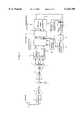
- FIG. 1is a block diagram illustrating a radio data communication terminal with a phase-locked loop circuit according to an embodiment of the present invention
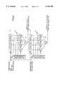
- FIG. 2is a block diagram illustrating in detail the replica signal generator 15 of FIG. 1;
- FIG. 3is a block diagram illustrating in detail the phase difference detector of FIG. 1;
- FIG. 4is a block diagram illustrating a conventional phase-locked loop circuit.
- FIG. 1is a block circuit diagram showing a radio data communication terminal including a phase-locked loop circuit which uses an equalizer, according to an embodiment of the present invention.
- the radio data communication terminalincludes an antenna 1 for receiving radio waves transmitted from a receiver side, a bandpass filter 2 for extracting signal components within a desired band from a received signal, an amplifier 3 for amplifying a signal passed through the bandpass filter 2 to a desired level, a mixer 4 used to down-convert a signal into a signal of a desired frequency, an oscillator 5 for generating a signal of a desired frequency, an amplifier 6 for amplifying a signal to a desired level, mixers 7 and 8 each for performing orthogonal demodulation, a 0/90° phase generator 9, an oscillator 10, and an A/D converter 11 for converting into a digital form a real part amplitude value orthogonally demodulated, an A/D converter 12 for converting into a digital form an imaginary part amplitude value orthogonally demodulated.
- the radio data communication terminalfurther includes an equalizer 14 for obtaining a tap coefficient desired for equalization and then demodulating the receive signal based on the tap coefficient.
- the radio data communication terminalstill further includes a phase rotation section 13, or phase correction means, for rotating the phase of a receive signal by a desired phase component, a replica signal generator 15, or receive signal generating means, for reproducing a received signal before demodulation based on demodulated data, a signal delay section 16, or timing means, for delaying a received signal to be input to the equalizer 14 to match it with the timing of the output signal from the replica signal generator 15 in symbol units, a phase difference detector 17, or phase difference detecting means, for providing the difference between the phase of the receive signal to be input to the equalizer and the phase of the output signal of the replica signal generator 15, a division section 18, or weighting means, for weighting the phase differences in a given ratio to remove an influence of distortion due to noises, an integration circuit 19, or integrating means, for integrating weighted values in symbol units, and a vector converter 20, or
- a radio sectionconsists of the antenna 1, the bandpass filter 2, the amplifier 3, the mixer 4, the oscillator 5, amplifier 6, the mixers 7 and 8, the phase generator 9, the oscillator 10, and the A/D converters 11 and 12.
- the radio sectionproduces an I signal component (an imaginary part amplitude value) and a Q signal component (a real part amplitude value) each orthogonally modulated.
- the equalizer 14obtains a transmission line characteristic based on the I and Q signal components during a preamble period.
- the tap coefficients determined based on the transmission line characteristicare set to the equalizer 14 and the replica signal generator 15.
- the equalizer 14starts to demodulate data.
- the replica signal generator 15sequentially receives data demodulated by the equalizer 14 and then reproduces the I and Q signal components input to the equalizer 14 based on the demodulated data and the tap coefficients.
- phase errorscan be obtained because of a time difference between the reproduced I signal component and the I signal component to be input to the equalizer 14 adjusted in timing by the signal delay section 16 and a time difference between the reproduced Q signal component and the Q signal component to be input to the equalizer 14 adjusted in timing by the signal delay section 16.
- the phase difference ( ⁇ ) in symbol unitcan be obtained by inputting the I and Q signal components to the phase difference detector 17.
- the division section 18implements an arbitrary weighting operation to determine the loop gain. A large loop gain provides a fast response characteristic but causes a large influence of noises.
- a small loop gainprovides a slow response characteristic but reduces an influence of noises.
- the vector converter 20converts the integration result into received signal components (a cosine value and a sine value).
- the phase rotation section 13receives the received signal components and then controllably rotates it, thus correcting the phase error.
- the vector conversioncan be performed using, for example, a ROM.
- FIG. 2is a block diagram illustrating the replica signal generator 15.
- This embodimentshows a replica signal generator having the characteristics for 4 symbols.
- the replica signal generator 15consists of shift registers 21 and 25 each for shifting and storing data demodulated by the equalizer 14 on a symbol-by-symbol basis, a real part tap coefficient storage section 22 for storing tap coefficients determined by transmission line characteristics, an imaginary part tap coefficient storage section 26 for storing tap coefficients determined by transmission line characteristics, multipliers 23 each for multiplying a tap coefficient by demodulated data, multipliers 27 each for multiplying a tap coefficient by demodulated data, adder 24 for adding multiplication results from the multipliers 23, and adder 28 for adding multiplication results from the multipliers 27.
- FIG. 3is a block diagram illustrating in detail the phase difference detector 17.
- the phase difference detector 17consists of multipliers 31 and 32 each for multiplying the signal from the signal delay section 16 by the signal from the replica signal generator 15, and a subtracter for providing the difference between a multiplication result of the multiplier 31 from a multiplication result of the multiplier 32.
- Tap coefficients of a real part determined based on the transmission characteristicare stored into the tap coefficient storage section 22 (with 4 taps in this example).
- Tap coefficients of an imaginary part determined based on the transmission characteristicare stored into the tap coefficient storage section 26 (with 4 taps in this example).
- Each of the multipliers 23multiplies each of tap coefficients stored in symbol units by each piece of demodulated data input to the shift register 21.
- Each of the multipliers 27multiplies each of tap coefficients stored in symbol units by each pieces of demodulated data input to the shift register 25.
- the real part amplitude value before demodulationcan be reproduced by adding the multiplication results by the adder 24.
- the imaginary part amplitude value before demodulationcan be reproduced by adding the multiplication results by the adder 28.
- the signal delay section 16In operation of the phase difference detector 17, the signal delay section 16 outputs the I output signal represented as r1 sin ⁇ 1 and the Q output signal represented as r1 cos ⁇ 1.
- the replica signal generator 15outputs the I output signal represented as r2 sin ⁇ 2 and the Q output signal represented as r2 cos ⁇ 2.
- the present inventionrelates to a phase-locked loop circuit that corrects the effect due to a phase error on a radio data communication terminal of the type that obtains a transmission line characteristic during a preamble period in a narrow band modulation mode and equalizes received signals.
- Phase controlcan be implemented during an receiving operation even in an environment of frequency selective multipath fading, so that cost reduction and expanded communication environment can be accomplished.
Landscapes
- Engineering & Computer Science (AREA)
- Computer Networks & Wireless Communication (AREA)
- Signal Processing (AREA)
- Power Engineering (AREA)
- Digital Transmission Methods That Use Modulated Carrier Waves (AREA)
- Synchronisation In Digital Transmission Systems (AREA)
Abstract
Description
The present invention relates to a phase-locked loop circuit that corrects an influence due to a shift in phase during a receiving operation of received signals by a radio data communication terminal in which received signals are equalized by obtaining a transmission line characteristic during a preamble period in a narrow band modulation mode such as the GMSK (Gaussian filtered Minimum Shift Keying) modulation mode. The present invention also relates to a phase locking method.
In many cases, it has been often difficult to use a synthesizer or crystal oscillator with excellent oscillation precision used to generate radio frequency signals. For that reason, a phase-locked loop circuit is normally used in the radio section or baseband section to establish communication under phase error control.
FIG. 4 is a block circuit diagram illustrating a conventional phase-locked loop circuit for BPSK (Binary Phase Shift Keying) modulation. The phased-locked loop circuit consists of aphase comparison circuit 41 for comparing the phase of a received input signal with a remodulated signal, aloop filter 42, avariable frequency oscillator 43, and aremodulation circuit 44 for remodulating demodulated signals.
The BPSK modulation input signal is represented as COS (2πft+aπ) (where f is a carrier frequency and a is a transmission digital signal). The output signal from thevariable frequency oscillator 43 is represented as COS (2πft+aπ+ΔΦ). The signal COS (2πft+ΔΦ+bΔ) is obtained by modulating the output signal COS (2πft+aπ+ΔΦ) with a received digital signal b. Thephase comparator 41 compares the two signals and then produces a signal (2πft+b)-(2πft+ΔΦ+aπ)(=(b-a)π-ΔΦ). If the received digital signal does not contain an error, a=b. Hence, thephase comparator 41 outputs -ΔΦ to cancel the phase error ΔΦ of thevariable frequency oscillator 43.
However, the problem is that the conventional phase-locked loop circuit cannot normally receive the modulated signal because the frequency spectrum collapses or becomes asymmetrical in the environment subjected to an influence of a frequency selective multipath fading.
The objective of the present invention is to solve the above-mentioned tasks.
The present invention is made to solve the above-mentioned problems. The objective of the present invention is to provide a phase-locked loop circuit that can correct an influence due to a phase error even in an environment of frequency selective multipath fading, suited for a radio data communication terminal which equalizes receive signals by a transmission line characteristic during preamble in a narrow band modulation mode.
Another objective of the present invention is to provide a phase locking method that can correct an influence due to a phase error even in an environment of frequency selective multipath fading.
The objective of the present invention is achieved by a phase-locked loop circuit comprising received signal reproducing means for reproducing a real part amplitude value and an imaginary part amplitude value based on tap coefficients set to the equalizer and data demodulated by the equalizer, the real part amplitude value and the imaginary part amplitude value each being a received signal before demodulation, timing means for providing timing to a reproduced received signal obtained by delaying and reproducing the receive signal, phase difference detecting means for detecting a phase difference between the reproduced received signal and the delayed received signal before demodulation, weighting means for weighting in a given ratio to remove an influence of distortion due to noises, integrating means for integrating the phase difference in symbol units, vector converting means for converting an integrated value into a cosine value and a sine value, and phase correcting means for correcting the phase of the demodulated received signal based on the cosine value and the sine value.
According to the present invention, in a radio data communication terminal which determines a transmission line characteristic during a preamble period and then implements demodulation by inputting a received signal to an equalizer based on the transmission line characteristic, phase correction is performed by reproducing a received signal before inputting the equalizer based on demodulation data obtained by the equalizer and a tap coefficient obtained for the equalizer and then comparing the resultant reproduced signal with signal components to be input to the equalizer to determine a phase difference.
In the phase-locked loop circuit according to the present invention, the receive signal reproducing circuit comprises a first shift register having stages corresponding to the number of symbols of the transmission line characteristic, for shifting and storing demodulation data demodulated by the equalizer in one symbol unit, a second shift register having stages corresponding to the number of symbols of the transmission line characteristic, for shifting and storing demodulation data demodulated by the equalizer in one symbol unit, a first tap coefficient storage section for storing real part tap coefficients determined by the transmission line characteristic, a second tap coefficient storage section for storing imaginary part tap coefficients determined by the transmission line characteristic, a first multiplier group for respectively multiplying various demodulation data output in parallel from the first shift register by the tap coefficients of the first tap coefficient storage section, a first adder for adding respective multiplication results from the first multiplier group, a second multiplier group for respectively multiplying various demodulation data output in parallel from the first shift register by the tap coefficients of the second tap coefficient storage section, and a second adder for adding respective multiplication results from the second multiplier group.
Moreover, in the phase-locked loop circuit according to the present invention, the phase difference detecting means comprises a first multiplier for multiplying a real part amplitude value of an output signal from the timing means by an imaginary part amplitude value from the received signal reproducing means, a second multiplier for multiplying an imaginary part amplitude value of the output signal from the timing means by a real part amplitude value from the received signal reproducing means, and a subtracter for subtracting a multiplication result from the first multiplier from a multiplication result from the second multiplier.
In the phase-locked loop circuit of the present invention, the receive signal reproducing circuit comprises a replica signal generator.
In the phase-locked loop circuit of the present invention, the timing means comprises a signal delay section.
In the phase-locked loop circuit of the present invention, the weighting means comprises a division section.
In the phase-locked loop circuit of the present invention, the phase correcting means comprises a phase rotation section.
In the phase-locked loop circuit of the present invention, the narrow band modulation mode is a GMSK modulation mode.
According to the present invention, a phase locking method by which an influence due to a phase error is corrected on a radio data communication terminal which equalizes received signals by obtaining a transmission line characteristic during a preamble duration in a narrow band modulation mode, comprising the steps of reproducing a real part amplitude value and an imaginary part amplitude value based on tap coefficients set to an equalizer and data demodulated by the equalizer, the real part amplitude value and the imaginary part amplitude value each being a received signal before demodulation, providing timing to a reproduced received signal obtained by delaying and reproducing the receive signal, detecting means for detecting a phase difference between the reproduced received signal and the delayed received signal before demodulation, weighting in a given ratio to remove an influence of distortion due to noises, integrating the phase difference in symbol units, converting an integrated value into a cosine value and a sine value, and correcting the phase of the demodulated received signal based on the cosine value and the sine value.
In the phase locking method of the present invention, the reproducing step comprises the steps of shifting and storing demodulation data demodulated by the equalizer in one symbol unit, storing real part tap coefficients determined by the transmission line characteristic, respectively multiplying the shifted demodulation data output in parallel by the real part tap coefficients, adding respective multiplication results to obtain a reproduced real part amplitude value, storing imaginary part tap coefficients determined by the transmission line characteristic, respectively multiplying the shifted demodulation data output in parallel by the imaginary part tap coefficients, and adding respective multiplication results to obtain a reproduced imaginary part amplitude value.
In the phase locking method of the present invention, the phase difference detecting step comprises the steps of firstly multiplying a real part amplitude value of an output signal in the timing providing step by an imaginary part amplitude value in said reproducing step, secondly multiplying an imaginary part amplitude value of said output signal in the timing providing step by a real part amplitude value in the reproducing step, and subtracting a multiplication result in the firstly multiplying step from a multiplication result in the secondly multiplying step.
This and other objects, features and advantages of the present invention will become more apparent upon a reading of the following detailed description and drawings, in which:
FIG. 1 is a block diagram illustrating a radio data communication terminal with a phase-locked loop circuit according to an embodiment of the present invention;
FIG. 2 is a block diagram illustrating in detail thereplica signal generator 15 of FIG. 1;
FIG. 3 is a block diagram illustrating in detail the phase difference detector of FIG. 1; and
FIG. 4 is a block diagram illustrating a conventional phase-locked loop circuit.
Next, an embodiment of the present invention will be described below in detail with reference to the attached drawings.
FIG. 1 is a block circuit diagram showing a radio data communication terminal including a phase-locked loop circuit which uses an equalizer, according to an embodiment of the present invention.
The radio data communication terminal includes anantenna 1 for receiving radio waves transmitted from a receiver side, abandpass filter 2 for extracting signal components within a desired band from a received signal, an amplifier 3 for amplifying a signal passed through thebandpass filter 2 to a desired level, amixer 4 used to down-convert a signal into a signal of a desired frequency, an oscillator 5 for generating a signal of a desired frequency, an amplifier 6 for amplifying a signal to a desired level,mixers phase generator 9, anoscillator 10, and an A/D converter 11 for converting into a digital form a real part amplitude value orthogonally demodulated, an A/D converter 12 for converting into a digital form an imaginary part amplitude value orthogonally demodulated. The radio data communication terminal further includes anequalizer 14 for obtaining a tap coefficient desired for equalization and then demodulating the receive signal based on the tap coefficient. The radio data communication terminal still further includes aphase rotation section 13, or phase correction means, for rotating the phase of a receive signal by a desired phase component, areplica signal generator 15, or receive signal generating means, for reproducing a received signal before demodulation based on demodulated data, asignal delay section 16, or timing means, for delaying a received signal to be input to theequalizer 14 to match it with the timing of the output signal from thereplica signal generator 15 in symbol units, aphase difference detector 17, or phase difference detecting means, for providing the difference between the phase of the receive signal to be input to the equalizer and the phase of the output signal of thereplica signal generator 15, adivision section 18, or weighting means, for weighting the phase differences in a given ratio to remove an influence of distortion due to noises, anintegration circuit 19, or integrating means, for integrating weighted values in symbol units, and avector converter 20, or vector converting means, for converting the output of theintegration circuit 19 into a cosine value and sine value. The phase locked loop circuit consists of thereplica signal generator 15, thesignal delay section 16, thephase rotation section 13, thephase difference detector 17, thedivider 18, theintegrator 19, and thevector converter 20.
A radio section consists of theantenna 1, thebandpass filter 2, the amplifier 3, themixer 4, the oscillator 5, amplifier 6, themixers phase generator 9, theoscillator 10, and the A/D converters equalizer 14 obtains a transmission line characteristic based on the I and Q signal components during a preamble period. The tap coefficients determined based on the transmission line characteristic are set to theequalizer 14 and thereplica signal generator 15. Theequalizer 14 starts to demodulate data. Thereplica signal generator 15 sequentially receives data demodulated by theequalizer 14 and then reproduces the I and Q signal components input to theequalizer 14 based on the demodulated data and the tap coefficients. Thus, phase errors can be obtained because of a time difference between the reproduced I signal component and the I signal component to be input to theequalizer 14 adjusted in timing by thesignal delay section 16 and a time difference between the reproduced Q signal component and the Q signal component to be input to theequalizer 14 adjusted in timing by thesignal delay section 16. The phase difference (Δθ) in symbol unit can be obtained by inputting the I and Q signal components to thephase difference detector 17. Thedivision section 18 implements an arbitrary weighting operation to determine the loop gain. A large loop gain provides a fast response characteristic but causes a large influence of noises. A small loop gain provides a slow response characteristic but reduces an influence of noises. After theintegration circuit 19 integrates phase differences in symbol units to convert the resultant phase difference into a frequency, thevector converter 20 converts the integration result into received signal components (a cosine value and a sine value). Thephase rotation section 13 receives the received signal components and then controllably rotates it, thus correcting the phase error. The vector conversion can be performed using, for example, a ROM.
FIG. 2 is a block diagram illustrating thereplica signal generator 15. This embodiment shows a replica signal generator having the characteristics for 4 symbols. Thereplica signal generator 15 consists ofshift registers equalizer 14 on a symbol-by-symbol basis, a real part tapcoefficient storage section 22 for storing tap coefficients determined by transmission line characteristics, an imaginary part tapcoefficient storage section 26 for storing tap coefficients determined by transmission line characteristics,multipliers 23 each for multiplying a tap coefficient by demodulated data,multipliers 27 each for multiplying a tap coefficient by demodulated data, adder 24 for adding multiplication results from themultipliers 23, and adder 28 for adding multiplication results from themultipliers 27. FIG. 3 is a block diagram illustrating in detail thephase difference detector 17. Thephase difference detector 17 consists ofmultipliers signal delay section 16 by the signal from thereplica signal generator 15, and a subtracter for providing the difference between a multiplication result of themultiplier 31 from a multiplication result of themultiplier 32.
First, an operation of thereplica signal generator 15 will be described here. Tap coefficients of a real part determined based on the transmission characteristic are stored into the tap coefficient storage section 22 (with 4 taps in this example). Tap coefficients of an imaginary part determined based on the transmission characteristic are stored into the tap coefficient storage section 26 (with 4 taps in this example). Each of themultipliers 23 multiplies each of tap coefficients stored in symbol units by each piece of demodulated data input to theshift register 21. Each of themultipliers 27 multiplies each of tap coefficients stored in symbol units by each pieces of demodulated data input to theshift register 25. The real part amplitude value before demodulation can be reproduced by adding the multiplication results by theadder 24. The imaginary part amplitude value before demodulation can be reproduced by adding the multiplication results by theadder 28.
In operation of thephase difference detector 17, thesignal delay section 16 outputs the I output signal represented as r1 sin θ1 and the Q output signal represented as r1 cos θ1. Thereplica signal generator 15 outputs the I output signal represented as r2 sin θ2 and the Q output signal represented as r2 cos θ2. Thus, the subtraction result of thesubtracter 33 satisfies the formula of r1 sin θ 1r2 cos θ2-r1 cos θ1 r2 sin θ2=r1r2 sin (θ1-θ2). If θ1 is near1y equal to θ2, it is regarded as sin (θ1-θ2)=θ1-θ2, so that the phase difference (θ1-θ2) can be obtained.
As described above, the present invention relates to a phase-locked loop circuit that corrects the effect due to a phase error on a radio data communication terminal of the type that obtains a transmission line characteristic during a preamble period in a narrow band modulation mode and equalizes received signals. Phase control can be implemented during an receiving operation even in an environment of frequency selective multipath fading, so that cost reduction and expanded communication environment can be accomplished.
The entire disclosure of Japanese Patent Application No. 9-135454 filed on May 26, 1997 including specification, claims, drawing and summary are incorporated herein by reference in its entirety.
Claims (11)
1. A phase-locked loop circuit with an equalizer, said phase-locked loop circuit that corrects an influence due to a phase error on a radio data communication terminal which equalizes received signals by obtaining a transmission line characteristic during a preamble duration in a narrow band modulation mode, comprising:
received signal reproducing means for reproducing a real part amplitude value and an imaginary part amplitude value based on tap coefficients set to said equalizer and data demodulated by said equalizer, said real part amplitude value and said imaginary part amplitude value each being a received signal before demodulation;
timing means for providing timing to a reproduced received signal obtained by delaying and reproducing said receive signal;
phase difference detecting means for detecting a phase difference between said reproduced received signal and said delayed received signal before demodulation;
weighting means for weighting in a given ratio to remove an influence of distortion due to noises;
integrating means for integrating the phase difference in symbol units;
vector converting means for converting an integrated value into a cosine value and a sine value; and
phase correcting means for correcting the phase of said demodulated received signal based on said cosine value and said sine value.
2. The phase-locked loop circuit defined in claim 1, wherein said receive signal reproducing circuit comprises:
a first shift register having stages corresponding to the number of symbols of said transmission line characteristic, for shifting and storing demodulation data demodulated by said equalizer in one symbol unit;
a second shift register having stages corresponding to the number of symbols of said transmission line characteristic, for shifting and storing demodulation data demodulated by said equalizer in one symbol unit;
a first tap coefficient storage section for storing real part tap coefficients determined by said transmission line characteristic;
a second tap coefficient storage section for storing imaginary part tap coefficients determined by said transmission line characteristic;
a first multiplier group for respectively multiplying various demodulation data output in parallel from said first shift register by said tap coefficients of said first tap coefficient storage section;
a first adder for adding respective multiplication results from said first multiplier group;
a second multiplier group for respectively multiplying various demodulation data output in parallel from said first shift register by said tap coefficients of said second tap coefficient storage section; and
a second adder for adding respective multiplication results from said second multiplier group.
3. The phase-locked loop circuit defined in claim 1, wherein said phase difference detecting means comprises:
a first multiplier for multiplying a real part amplitude value of an output signal from said timing means by an imaginary part amplitude value from said received signal reproducing means;
a second multiplier for multiplying an imaginary part amplitude value of said output signal from said timing means by a real part amplitude value from said received signal reproducing means; and
a subtracter for subtracting a multiplication result from said first multiplier from a multiplication result from said second multiplier.
4. The phase-locked loop circuit defined in claim 1, wherein said receive signal reproducing circuit comprises a replica signal generator.
5. The phase-locked loop circuit defined in claim 1, wherein said timing means comprises a signal delay section.
6. The phase-locked loop circuit defined in claim 1, wherein said weighting means comprises a division section.
7. The phase-locked loop circuit defined in claim 1, wherein said phase correcting means comprises a phase rotation section.
8. The phase-locked loop circuit defined in claim 1, wherein said narrow band modulation mode is a GMSK modulation mode.
9. A phase locking method by which an influence due to a phase error is corrected on a radio data communication terminal which equalizes received signals by obtaining a transmission line characteristic during a preamble duration in a narrow band modulation mode, comprising the steps of:
reproducing a real part amplitude value and an imaginary part amplitude value based on tap coefficients set to an equalizer and data demodulated by said equalizer; said real part amplitude value and said imaginary part amplitude value each being a received signal before demodulation;
providing a timing to a reproduced received signal obtained by delaying and reproducing said receive signal;
detecting means for detecting a phase difference between said reproduced received signal and said delayed received signal before demodulation;
weighting in a given ratio to remove an influence of distortion due to noises;
integrating the phase difference in symbol units, converting an integrated value into a cosine value and a sine value; and
correcting the phase of said demodulated received signal based on said cosine value and said sine value.
10. The phase locking method defined in claim 9, wherein said reproducing step comprises the steps of:
shifting and storing demodulation data demodulated by said equalizer in one symbol unit;
storing real part tap coefficients determined by said transmission line characteristic;
respectively multiplying said shifted demodulation data output in parallel by said real part tap coefficients, adding respective multiplication results to obtain a reproduced real part amplitude value;
storing imaginary part tap coefficients determined by said transmission line characteristic;
respectively multiplying said shifted demodulation data output in parallel by said imaginary part tap coefficients; and
adding respective multiplication results to obtain a reproduced imaginary part amplitude value.
11. The phase locking method defined in claim 9, wherein said phase difference detecting step comprises the steps of:
firstly multiplying a real part amplitude value of an output signal in said timing providing step by an imaginary part amplitude value in said reproducing step;
secondly multiplying an imaginary part amplitude value of said output signal in said timing providing step by a real part amplitude value in said reproducing step; and
subtracting a multiplication result in said firstly multiplying step from a multiplication result in said secondly multiplying step.
Applications Claiming Priority (2)
| Application Number | Priority Date | Filing Date | Title |
|---|---|---|---|
| JP9-135454 | 1997-05-26 | ||
| JP9135454AJPH10327204A (en) | 1997-05-26 | 1997-05-26 | Phase locked loop circuit using equalizer |
Publications (1)
| Publication Number | Publication Date |
|---|---|
| US6144708Atrue US6144708A (en) | 2000-11-07 |
Family
ID=15152098
Family Applications (1)
| Application Number | Title | Priority Date | Filing Date |
|---|---|---|---|
| US09/083,342Expired - LifetimeUS6144708A (en) | 1997-05-26 | 1998-05-22 | Phase-locked loop circuit with equalizer and phase locking method |
Country Status (2)
| Country | Link |
|---|---|
| US (1) | US6144708A (en) |
| JP (1) | JPH10327204A (en) |
Cited By (44)
| Publication number | Priority date | Publication date | Assignee | Title |
|---|---|---|---|---|
| US20020136343A1 (en)* | 2001-01-16 | 2002-09-26 | International Business Machines Corporation | Analog unidirectional serial link architecture |
| US6522702B1 (en)* | 1998-04-22 | 2003-02-18 | Nec Corporation | Radio data communication terminal |
| US6587521B1 (en)* | 1998-12-17 | 2003-07-01 | Nec Corporation | Signal estimator and program stored memory medium |
| US20030143967A1 (en)* | 2002-01-25 | 2003-07-31 | Ciccarelli Steven C. | AMPS receiver system using a zero-IF architecture |
| US6614840B1 (en)* | 1999-03-16 | 2003-09-02 | Nec Corporation | Equalizer with phase-locked loop |
| US6622006B1 (en)* | 2000-02-02 | 2003-09-16 | Hughes Electronics Corporation | System and method for detecting a link outage |
| WO2002096099A3 (en)* | 2001-05-11 | 2003-09-25 | Koninkl Philips Electronics Nv | Quadrature demodulator |
| EP1361655A1 (en)* | 2002-05-07 | 2003-11-12 | Semiconductor Ideas to The Market (ItoM) BV | Mirror suppression circuit in a quadrature demodulator |
| WO2003047092A3 (en)* | 2001-11-27 | 2003-12-11 | Qualcomm Inc | Direct conversion of narrow-band rf signals |
| US20040066871A1 (en)* | 2002-10-07 | 2004-04-08 | Cranford Hayden C. | Digital adaptive control loop for data deserialization |
| US20040071234A1 (en)* | 2002-07-18 | 2004-04-15 | Oki Techno Centre (Singapore) Pte Ltd | High rate receiver |
| US6731698B1 (en)* | 1999-03-25 | 2004-05-04 | Sanyo Electric Co., Ltd. | Quadrature demodulation circuit capable for canceling offset |
| US6944244B2 (en) | 2001-09-18 | 2005-09-13 | Thomson Licensing S.A. | Mechanism for OFDM equalizer tap initialization using an adaptive algorithm |
| US20060268973A1 (en)* | 2005-05-31 | 2006-11-30 | Ganning Yang | GFSK/GMSK detector with enhanced performance in co-channel interference and AWGN channels |
| US7151807B2 (en) | 2001-04-27 | 2006-12-19 | The Directv Group, Inc. | Fast acquisition of timing and carrier frequency from received signal |
| US20070024383A1 (en)* | 2005-07-28 | 2007-02-01 | Zarlink Semiconductor Inc. | Phase Locked Loop Fast Lock Method |
| US7173981B1 (en) | 2001-04-27 | 2007-02-06 | The Directv Group, Inc. | Dual layer signal processing in a layered modulation digital signal system |
| US7173977B2 (en) | 2002-10-25 | 2007-02-06 | The Directv Group, Inc. | Method and apparatus for tailoring carrier power requirements according to availability in layered modulation systems |
| US7184473B2 (en) | 2001-04-27 | 2007-02-27 | The Directv Group, Inc. | Equalizers for layered modulated and other signals |
| US7184489B2 (en) | 2001-04-27 | 2007-02-27 | The Directv Group, Inc. | Optimization technique for layered modulation |
| US7209524B2 (en) | 2001-04-27 | 2007-04-24 | The Directv Group, Inc. | Layered modulation for digital signals |
| US20070117511A1 (en)* | 2005-11-18 | 2007-05-24 | Samsung Electronics Co., Ltd. | RF receiving apparatus and method for removing leakage component of received signal using local signal |
| US7230480B2 (en) | 2002-10-25 | 2007-06-12 | The Directv Group, Inc. | Estimating the operating point on a non-linear traveling wave tube amplifier |
| US7245671B1 (en) | 2001-04-27 | 2007-07-17 | The Directv Group, Inc. | Preprocessing signal layers in a layered modulation digital signal system to use legacy receivers |
| US7418060B2 (en) | 2002-07-01 | 2008-08-26 | The Directv Group, Inc. | Improving hierarchical 8PSK performance |
| US7423987B2 (en) | 2001-04-27 | 2008-09-09 | The Directv Group, Inc. | Feeder link configurations to support layered modulation for digital signals |
| US7463676B2 (en) | 2002-10-25 | 2008-12-09 | The Directv Group, Inc. | On-line phase noise measurement for layered modulation |
| US7471735B2 (en) | 2001-04-27 | 2008-12-30 | The Directv Group, Inc. | Maximizing power and spectral efficiencies for layered and conventional modulations |
| US7474710B2 (en) | 2002-10-25 | 2009-01-06 | The Directv Group, Inc. | Amplitude and phase matching for layered modulation reception |
| US7483505B2 (en) | 2001-04-27 | 2009-01-27 | The Directv Group, Inc. | Unblind equalizer architecture for digital communication systems |
| US7502429B2 (en) | 2003-10-10 | 2009-03-10 | The Directv Group, Inc. | Equalization for traveling wave tube amplifier nonlinearity measurements |
| US7502430B2 (en) | 2001-04-27 | 2009-03-10 | The Directv Group, Inc. | Coherent averaging for measuring traveling wave tube amplifier nonlinearity |
| US7512189B2 (en) | 2001-04-27 | 2009-03-31 | The Directv Group, Inc. | Lower complexity layered modulation signal processor |
| US7529312B2 (en) | 2002-10-25 | 2009-05-05 | The Directv Group, Inc. | Layered modulation for terrestrial ATSC applications |
| US7583728B2 (en) | 2002-10-25 | 2009-09-01 | The Directv Group, Inc. | Equalizers for layered modulated and other signals |
| US7639759B2 (en) | 2001-04-27 | 2009-12-29 | The Directv Group, Inc. | Carrier to noise ratio estimations from a received signal |
| US20100105319A1 (en)* | 2008-10-23 | 2010-04-29 | Pericom Semiconductor Corp. | Redriver with Output Receiver Detection that Mirrors Detected Termination on Output to Input |
| US7738587B2 (en) | 2002-07-03 | 2010-06-15 | The Directv Group, Inc. | Method and apparatus for layered modulation |
| US7778365B2 (en)* | 2001-04-27 | 2010-08-17 | The Directv Group, Inc. | Satellite TWTA on-line non-linearity measurement |
| US7822154B2 (en) | 2001-04-27 | 2010-10-26 | The Directv Group, Inc. | Signal, interference and noise power measurement |
| US8005035B2 (en) | 2001-04-27 | 2011-08-23 | The Directv Group, Inc. | Online output multiplexer filter measurement |
| US20130111307A1 (en)* | 2011-10-31 | 2013-05-02 | Dacheng Zhou | Receiver With Tap-Coefficient Adjustments |
| US11206170B2 (en)* | 2018-12-19 | 2021-12-21 | Nxp B.V. | Communications device and method for operating a communications device |
| US20220376792A1 (en)* | 2019-07-29 | 2022-11-24 | Nec Corporation | Re-modulation device, demodulation reception device, modulation transmission device, modulation communication system, re-modulation method, and recording medium |
Families Citing this family (3)
| Publication number | Priority date | Publication date | Assignee | Title |
|---|---|---|---|---|
| JP3206550B2 (en) | 1998-05-11 | 2001-09-10 | 日本電気株式会社 | Signal estimator with phase locked loop |
| JP3377035B2 (en)* | 1998-12-04 | 2003-02-17 | 日本電気株式会社 | Phase locked loop circuit using signal estimator |
| JP2007325163A (en)* | 2006-06-05 | 2007-12-13 | Japan Radio Co Ltd | Signal decomposition apparatus and signal amplification system |
Citations (4)
| Publication number | Priority date | Publication date | Assignee | Title |
|---|---|---|---|---|
| US4647984A (en)* | 1984-04-12 | 1987-03-03 | Pioneer Electronic Corporation | Time axis deviation compensation apparatus |
| US4918393A (en)* | 1987-11-18 | 1990-04-17 | Hitachi, Ltd. | Phase control device |
| US5999542A (en)* | 1995-08-18 | 1999-12-07 | Adtran, Inc. | Use of modified line encoding and low signal-to-noise ratio based signal processing to extend range of digital data transmission over repeaterless two-wire telephone link |
| US6002717A (en)* | 1997-03-06 | 1999-12-14 | National Semiconductor Corporation | Method and apparatus for adaptive equalization using feedback indicative of undercompensation |
- 1997
- 1997-05-26JPJP9135454Apatent/JPH10327204A/enactivePending
- 1998
- 1998-05-22USUS09/083,342patent/US6144708A/ennot_activeExpired - Lifetime
Patent Citations (4)
| Publication number | Priority date | Publication date | Assignee | Title |
|---|---|---|---|---|
| US4647984A (en)* | 1984-04-12 | 1987-03-03 | Pioneer Electronic Corporation | Time axis deviation compensation apparatus |
| US4918393A (en)* | 1987-11-18 | 1990-04-17 | Hitachi, Ltd. | Phase control device |
| US5999542A (en)* | 1995-08-18 | 1999-12-07 | Adtran, Inc. | Use of modified line encoding and low signal-to-noise ratio based signal processing to extend range of digital data transmission over repeaterless two-wire telephone link |
| US6002717A (en)* | 1997-03-06 | 1999-12-14 | National Semiconductor Corporation | Method and apparatus for adaptive equalization using feedback indicative of undercompensation |
Cited By (70)
| Publication number | Priority date | Publication date | Assignee | Title |
|---|---|---|---|---|
| US6522702B1 (en)* | 1998-04-22 | 2003-02-18 | Nec Corporation | Radio data communication terminal |
| US6587521B1 (en)* | 1998-12-17 | 2003-07-01 | Nec Corporation | Signal estimator and program stored memory medium |
| US6614840B1 (en)* | 1999-03-16 | 2003-09-02 | Nec Corporation | Equalizer with phase-locked loop |
| US6731698B1 (en)* | 1999-03-25 | 2004-05-04 | Sanyo Electric Co., Ltd. | Quadrature demodulation circuit capable for canceling offset |
| US6622006B1 (en)* | 2000-02-02 | 2003-09-16 | Hughes Electronics Corporation | System and method for detecting a link outage |
| US20020136343A1 (en)* | 2001-01-16 | 2002-09-26 | International Business Machines Corporation | Analog unidirectional serial link architecture |
| US7142624B2 (en) | 2001-01-16 | 2006-11-28 | International Business Machines Corporation | Analog unidirectional serial link architecture |
| US6993107B2 (en) | 2001-01-16 | 2006-01-31 | International Business Machines Corporation | Analog unidirectional serial link architecture |
| US7426246B2 (en) | 2001-04-27 | 2008-09-16 | The Directv Group, Inc. | Dual layer signal processing in a layered modulation digital signal system |
| US7471735B2 (en) | 2001-04-27 | 2008-12-30 | The Directv Group, Inc. | Maximizing power and spectral efficiencies for layered and conventional modulations |
| US8259641B2 (en) | 2001-04-27 | 2012-09-04 | The Directv Group, Inc. | Feeder link configurations to support layered modulation for digital signals |
| US8208526B2 (en) | 2001-04-27 | 2012-06-26 | The Directv Group, Inc. | Equalizers for layered modulated and other signals |
| US8005035B2 (en) | 2001-04-27 | 2011-08-23 | The Directv Group, Inc. | Online output multiplexer filter measurement |
| US7920643B2 (en) | 2001-04-27 | 2011-04-05 | The Directv Group, Inc. | Maximizing power and spectral efficiencies for layered and conventional modulations |
| US7822154B2 (en) | 2001-04-27 | 2010-10-26 | The Directv Group, Inc. | Signal, interference and noise power measurement |
| US7778365B2 (en)* | 2001-04-27 | 2010-08-17 | The Directv Group, Inc. | Satellite TWTA on-line non-linearity measurement |
| US7706466B2 (en) | 2001-04-27 | 2010-04-27 | The Directv Group, Inc. | Lower complexity layered modulation signal processor |
| US7639759B2 (en) | 2001-04-27 | 2009-12-29 | The Directv Group, Inc. | Carrier to noise ratio estimations from a received signal |
| US7512189B2 (en) | 2001-04-27 | 2009-03-31 | The Directv Group, Inc. | Lower complexity layered modulation signal processor |
| US7502430B2 (en) | 2001-04-27 | 2009-03-10 | The Directv Group, Inc. | Coherent averaging for measuring traveling wave tube amplifier nonlinearity |
| US7151807B2 (en) | 2001-04-27 | 2006-12-19 | The Directv Group, Inc. | Fast acquisition of timing and carrier frequency from received signal |
| US7483495B2 (en) | 2001-04-27 | 2009-01-27 | The Directv Group, Inc. | Layered modulation for digital signals |
| US7173981B1 (en) | 2001-04-27 | 2007-02-06 | The Directv Group, Inc. | Dual layer signal processing in a layered modulation digital signal system |
| US7483505B2 (en) | 2001-04-27 | 2009-01-27 | The Directv Group, Inc. | Unblind equalizer architecture for digital communication systems |
| US7184473B2 (en) | 2001-04-27 | 2007-02-27 | The Directv Group, Inc. | Equalizers for layered modulated and other signals |
| US7184489B2 (en) | 2001-04-27 | 2007-02-27 | The Directv Group, Inc. | Optimization technique for layered modulation |
| US7209524B2 (en) | 2001-04-27 | 2007-04-24 | The Directv Group, Inc. | Layered modulation for digital signals |
| US7469019B2 (en) | 2001-04-27 | 2008-12-23 | The Directv Group, Inc. | Optimization technique for layered modulation |
| US7426243B2 (en) | 2001-04-27 | 2008-09-16 | The Directv Group, Inc. | Preprocessing signal layers in a layered modulation digital signal system to use legacy receivers |
| US7423987B2 (en) | 2001-04-27 | 2008-09-09 | The Directv Group, Inc. | Feeder link configurations to support layered modulation for digital signals |
| US7245671B1 (en) | 2001-04-27 | 2007-07-17 | The Directv Group, Inc. | Preprocessing signal layers in a layered modulation digital signal system to use legacy receivers |
| WO2002096099A3 (en)* | 2001-05-11 | 2003-09-25 | Koninkl Philips Electronics Nv | Quadrature demodulator |
| US6944244B2 (en) | 2001-09-18 | 2005-09-13 | Thomson Licensing S.A. | Mechanism for OFDM equalizer tap initialization using an adaptive algorithm |
| KR100954705B1 (en) | 2001-11-27 | 2010-04-23 | 퀄컴 인코포레이티드 | Direct conversion receiver |
| WO2003047092A3 (en)* | 2001-11-27 | 2003-12-11 | Qualcomm Inc | Direct conversion of narrow-band rf signals |
| US6775530B2 (en) | 2001-11-27 | 2004-08-10 | Qualcomm Inc. | Direct conversion of narrow-band RF signals |
| WO2004049580A3 (en)* | 2002-01-25 | 2005-11-17 | Qualcomm Inc | An amps receiver system using a zero-if architecture |
| EP2120351A1 (en)* | 2002-01-25 | 2009-11-18 | Qualcomm Incorporated | An AMPS receiver system using a zero-if architecture |
| US20030143967A1 (en)* | 2002-01-25 | 2003-07-31 | Ciccarelli Steven C. | AMPS receiver system using a zero-IF architecture |
| US7242730B2 (en)* | 2002-05-07 | 2007-07-10 | Semiconductor Ideas To Market, B.V. | Mirror suppression circuit and receiver using such circuit |
| EP1361655A1 (en)* | 2002-05-07 | 2003-11-12 | Semiconductor Ideas to The Market (ItoM) BV | Mirror suppression circuit in a quadrature demodulator |
| WO2003096524A3 (en)* | 2002-05-07 | 2004-05-13 | Semiconductor Ideas Market Bv | Mirror suppression circuit in a quadrature demodulator |
| US20050226352A1 (en)* | 2002-05-07 | 2005-10-13 | Kasperkovitz Wolfdietrich G | Mirror suppression circuit and receiver using such circuit |
| US7418060B2 (en) | 2002-07-01 | 2008-08-26 | The Directv Group, Inc. | Improving hierarchical 8PSK performance |
| US7577213B2 (en) | 2002-07-01 | 2009-08-18 | The Directv Group, Inc. | Hierarchical 8PSK performance |
| US7738587B2 (en) | 2002-07-03 | 2010-06-15 | The Directv Group, Inc. | Method and apparatus for layered modulation |
| US20040071234A1 (en)* | 2002-07-18 | 2004-04-15 | Oki Techno Centre (Singapore) Pte Ltd | High rate receiver |
| US7317777B2 (en) | 2002-10-07 | 2008-01-08 | International Business Machines Corporation | Digital adaptive control loop for data deserialization |
| US20040066871A1 (en)* | 2002-10-07 | 2004-04-08 | Cranford Hayden C. | Digital adaptive control loop for data deserialization |
| US7474710B2 (en) | 2002-10-25 | 2009-01-06 | The Directv Group, Inc. | Amplitude and phase matching for layered modulation reception |
| US7529312B2 (en) | 2002-10-25 | 2009-05-05 | The Directv Group, Inc. | Layered modulation for terrestrial ATSC applications |
| US7583728B2 (en) | 2002-10-25 | 2009-09-01 | The Directv Group, Inc. | Equalizers for layered modulated and other signals |
| US7173977B2 (en) | 2002-10-25 | 2007-02-06 | The Directv Group, Inc. | Method and apparatus for tailoring carrier power requirements according to availability in layered modulation systems |
| US7463676B2 (en) | 2002-10-25 | 2008-12-09 | The Directv Group, Inc. | On-line phase noise measurement for layered modulation |
| US7230480B2 (en) | 2002-10-25 | 2007-06-12 | The Directv Group, Inc. | Estimating the operating point on a non-linear traveling wave tube amplifier |
| US7502429B2 (en) | 2003-10-10 | 2009-03-10 | The Directv Group, Inc. | Equalization for traveling wave tube amplifier nonlinearity measurements |
| US7515665B2 (en)* | 2005-05-31 | 2009-04-07 | Skyworks Solutions, Inc. | GFSK/GMSK detector with enhanced performance in co-channel interference and AWGN channels |
| US20060268973A1 (en)* | 2005-05-31 | 2006-11-30 | Ganning Yang | GFSK/GMSK detector with enhanced performance in co-channel interference and AWGN channels |
| US7369002B2 (en) | 2005-07-28 | 2008-05-06 | Zarlink Semiconductor, Inc. | Phase locked loop fast lock method |
| US20070024383A1 (en)* | 2005-07-28 | 2007-02-01 | Zarlink Semiconductor Inc. | Phase Locked Loop Fast Lock Method |
| US7689170B2 (en)* | 2005-11-18 | 2010-03-30 | Samsung Electronics Co., Ltd. | RF receiving apparatus and method for removing leakage component of received signal using local signal |
| US20070117511A1 (en)* | 2005-11-18 | 2007-05-24 | Samsung Electronics Co., Ltd. | RF receiving apparatus and method for removing leakage component of received signal using local signal |
| US20100105319A1 (en)* | 2008-10-23 | 2010-04-29 | Pericom Semiconductor Corp. | Redriver with Output Receiver Detection that Mirrors Detected Termination on Output to Input |
| US8212587B2 (en) | 2008-10-23 | 2012-07-03 | Pericom Semiconductor Corp. | Redriver with output receiver detection that mirrors detected termination on output to input |
| US9094245B2 (en) | 2008-10-23 | 2015-07-28 | Pericom Semiconductor Corporation | Redriver with output receiver detection that mirrors detected termination on output to input |
| US20130111307A1 (en)* | 2011-10-31 | 2013-05-02 | Dacheng Zhou | Receiver With Tap-Coefficient Adjustments |
| US8966353B2 (en)* | 2011-10-31 | 2015-02-24 | Hewlett-Packard Development Company L.P. | Receiver with tap-coefficient adjustments |
| US11206170B2 (en)* | 2018-12-19 | 2021-12-21 | Nxp B.V. | Communications device and method for operating a communications device |
| US20220376792A1 (en)* | 2019-07-29 | 2022-11-24 | Nec Corporation | Re-modulation device, demodulation reception device, modulation transmission device, modulation communication system, re-modulation method, and recording medium |
| US11728892B2 (en)* | 2019-07-29 | 2023-08-15 | Nec Corporation | Re-modulation device, demodulation reception device, modulation transmission device, modulation communication system, re-modulation method, and recording medium |
Also Published As
| Publication number | Publication date |
|---|---|
| JPH10327204A (en) | 1998-12-08 |
Similar Documents
| Publication | Publication Date | Title |
|---|---|---|
| US6144708A (en) | Phase-locked loop circuit with equalizer and phase locking method | |
| US4085378A (en) | QPSK demodulator | |
| US5144256A (en) | Method and apparatus for demodulating a GMSK signal | |
| US6127884A (en) | Differentiate and multiply based timing recovery in a quadrature demodulator | |
| US5440267A (en) | Demodulator | |
| US5787123A (en) | Receiver for orthogonal frequency division multiplexed signals | |
| US5049830A (en) | Carrier recovery system and digital phase demodulator | |
| CA2078705C (en) | Method and arrangement of coherently demodulating psk signals using a feedback loop including a filter bank | |
| JPH05504458A (en) | adaptive phase-locked loop | |
| US6996193B2 (en) | Timing error detection circuit, demodulation circuit and methods thereof | |
| US5940451A (en) | Automatic gain control in quadrature phase shift keying demodulator | |
| CA2054173C (en) | Digital radio receiver having amplitude limiter and logarithmic detector | |
| JPH07321862A (en) | Digital modulated wave demodulator | |
| US4054838A (en) | QAM phase jitter and frequency offset correction system | |
| US4953186A (en) | Phase jitter tracker | |
| US5627861A (en) | Carrier phase estimation system using filter | |
| US20070127599A1 (en) | Apparatus and method for phase recovery and I/Q imbalance compensation in quadrature demodulating receiver | |
| JPH0621992A (en) | Demodulator | |
| US6456671B1 (en) | Decision feedback phase tracking demodulation | |
| JP3185872B2 (en) | Automatic gain control circuit | |
| US6396884B1 (en) | Automatic frequency control circuit | |
| EP0484914B1 (en) | Demodulator and method for demodulating digital signals modulated by a minimum shift keying | |
| US5572551A (en) | Carrier loop acquisition for staggered phase shift keying | |
| US7457375B2 (en) | Timing extractor, timing extraction method, and demodulator having the timing extractor | |
| US5982200A (en) | Costas loop carrier recovery circuit using square-law circuits |
Legal Events
| Date | Code | Title | Description |
|---|---|---|---|
| AS | Assignment | Owner name:NEC CORPORATION, JAPAN Free format text:ASSIGNMENT OF ASSIGNORS INTEREST;ASSIGNOR:MARUYAMA, HIDENORI;REEL/FRAME:009198/0350 Effective date:19980515 | |
| STCF | Information on status: patent grant | Free format text:PATENTED CASE | |
| FEPP | Fee payment procedure | Free format text:PAYOR NUMBER ASSIGNED (ORIGINAL EVENT CODE: ASPN); ENTITY STATUS OF PATENT OWNER: LARGE ENTITY | |
| FPAY | Fee payment | Year of fee payment:4 | |
| FPAY | Fee payment | Year of fee payment:8 | |
| FPAY | Fee payment | Year of fee payment:12 | |
| AS | Assignment | Owner name:RAKUTEN, INC., JAPAN Free format text:ASSIGNMENT OF ASSIGNORS INTEREST;ASSIGNOR:NEC CORPORATION;REEL/FRAME:028252/0280 Effective date:20120514 | |
| AS | Assignment | Owner name:RAKUTEN, INC., JAPAN Free format text:CHANGE OF ADDRESS;ASSIGNOR:RAKUTEN, INC.;REEL/FRAME:037751/0006 Effective date:20150824 |