US6144557A - Self-locking conductive pin for printed wiring substrate electronics case - Google Patents
Self-locking conductive pin for printed wiring substrate electronics caseDownload PDFInfo
- Publication number
- US6144557A US6144557AUS09/289,686US28968699AUS6144557AUS 6144557 AUS6144557 AUS 6144557AUS 28968699 AUS28968699 AUS 28968699AUS 6144557 AUS6144557 AUS 6144557A
- Authority
- US
- United States
- Prior art keywords
- case
- enclosure
- pin
- electrically conductive
- substrate
- Prior art date
- Legal status (The legal status is an assumption and is not a legal conclusion. Google has not performed a legal analysis and makes no representation as to the accuracy of the status listed.)
- Expired - Lifetime
Links
- 239000000758substrateSubstances0.000titleclaimsabstractdescription46
- 239000003989dielectric materialSubstances0.000claimsabstractdescription15
- 239000002184metalSubstances0.000claimsabstractdescription10
- 239000008393encapsulating agentSubstances0.000claimsdescription14
- 229910000679solderInorganic materials0.000claimsdescription4
- 239000000463materialSubstances0.000claims1
- 238000004519manufacturing processMethods0.000abstractdescription17
- 238000000034methodMethods0.000description18
- 230000006835compressionEffects0.000description2
- 238000007906compressionMethods0.000description2
- 238000010586diagramMethods0.000description2
- 238000005476solderingMethods0.000description2
- 239000004593EpoxySubstances0.000description1
- 239000000853adhesiveSubstances0.000description1
- 230000001070adhesive effectEffects0.000description1
- 230000004075alterationEffects0.000description1
- 238000010276constructionMethods0.000description1
- 230000007812deficiencyEffects0.000description1
- 230000009977dual effectEffects0.000description1
- 230000007613environmental effectEffects0.000description1
- 230000005669field effectEffects0.000description1
- 238000009413insulationMethods0.000description1
- 229910044991metal oxideInorganic materials0.000description1
- 150000004706metal oxidesChemical class0.000description1
- 238000004806packaging method and processMethods0.000description1
- 230000002093peripheral effectEffects0.000description1
- 229920000642polymerPolymers0.000description1
- 230000001681protective effectEffects0.000description1
- 239000004065semiconductorSubstances0.000description1
- 238000006467substitution reactionMethods0.000description1
- 238000003466weldingMethods0.000description1
Images


Classifications
- H—ELECTRICITY
- H05—ELECTRIC TECHNIQUES NOT OTHERWISE PROVIDED FOR
- H05K—PRINTED CIRCUITS; CASINGS OR CONSTRUCTIONAL DETAILS OF ELECTRIC APPARATUS; MANUFACTURE OF ASSEMBLAGES OF ELECTRICAL COMPONENTS
- H05K9/00—Screening of apparatus or components against electric or magnetic fields
- H05K9/0007—Casings
- H05K9/002—Casings with localised screening
- H05K9/0039—Galvanic coupling of ground layer on printed circuit board [PCB] to conductive casing
- H—ELECTRICITY
- H05—ELECTRIC TECHNIQUES NOT OTHERWISE PROVIDED FOR
- H05K—PRINTED CIRCUITS; CASINGS OR CONSTRUCTIONAL DETAILS OF ELECTRIC APPARATUS; MANUFACTURE OF ASSEMBLAGES OF ELECTRICAL COMPONENTS
- H05K1/00—Printed circuits
- H05K1/02—Details
- H05K1/14—Structural association of two or more printed circuits
- H05K1/141—One or more single auxiliary printed circuits mounted on a main printed circuit, e.g. modules, adapters
- H—ELECTRICITY
- H05—ELECTRIC TECHNIQUES NOT OTHERWISE PROVIDED FOR
- H05K—PRINTED CIRCUITS; CASINGS OR CONSTRUCTIONAL DETAILS OF ELECTRIC APPARATUS; MANUFACTURE OF ASSEMBLAGES OF ELECTRICAL COMPONENTS
- H05K1/00—Printed circuits
- H05K1/02—Details
- H05K1/0213—Electrical arrangements not otherwise provided for
- H05K1/0215—Grounding of printed circuits by connection to external grounding means
- H—ELECTRICITY
- H05—ELECTRIC TECHNIQUES NOT OTHERWISE PROVIDED FOR
- H05K—PRINTED CIRCUITS; CASINGS OR CONSTRUCTIONAL DETAILS OF ELECTRIC APPARATUS; MANUFACTURE OF ASSEMBLAGES OF ELECTRICAL COMPONENTS
- H05K2201/00—Indexing scheme relating to printed circuits covered by H05K1/00
- H05K2201/10—Details of components or other objects attached to or integrated in a printed circuit board
- H05K2201/10227—Other objects, e.g. metallic pieces
- H05K2201/10295—Metallic connector elements partly mounted in a hole of the PCB
- H05K2201/10303—Pin-in-hole mounted pins
- H—ELECTRICITY
- H05—ELECTRIC TECHNIQUES NOT OTHERWISE PROVIDED FOR
- H05K—PRINTED CIRCUITS; CASINGS OR CONSTRUCTIONAL DETAILS OF ELECTRIC APPARATUS; MANUFACTURE OF ASSEMBLAGES OF ELECTRICAL COMPONENTS
- H05K2201/00—Indexing scheme relating to printed circuits covered by H05K1/00
- H05K2201/10—Details of components or other objects attached to or integrated in a printed circuit board
- H05K2201/10227—Other objects, e.g. metallic pieces
- H05K2201/10371—Shields or metal cases
- H—ELECTRICITY
- H05—ELECTRIC TECHNIQUES NOT OTHERWISE PROVIDED FOR
- H05K—PRINTED CIRCUITS; CASINGS OR CONSTRUCTIONAL DETAILS OF ELECTRIC APPARATUS; MANUFACTURE OF ASSEMBLAGES OF ELECTRICAL COMPONENTS
- H05K2201/00—Indexing scheme relating to printed circuits covered by H05K1/00
- H05K2201/10—Details of components or other objects attached to or integrated in a printed circuit board
- H05K2201/10613—Details of electrical connections of non-printed components, e.g. special leads
- H05K2201/10742—Details of leads
- H05K2201/1075—Shape details
- H05K2201/10871—Leads having an integral insert stop
- H—ELECTRICITY
- H05—ELECTRIC TECHNIQUES NOT OTHERWISE PROVIDED FOR
- H05K—PRINTED CIRCUITS; CASINGS OR CONSTRUCTIONAL DETAILS OF ELECTRIC APPARATUS; MANUFACTURE OF ASSEMBLAGES OF ELECTRICAL COMPONENTS
- H05K3/00—Apparatus or processes for manufacturing printed circuits
- H05K3/30—Assembling printed circuits with electric components, e.g. with resistor
- H05K3/306—Lead-in-hole components, e.g. affixing or retention before soldering, spacing means
- H05K3/308—Adaptations of leads
- H—ELECTRICITY
- H05—ELECTRIC TECHNIQUES NOT OTHERWISE PROVIDED FOR
- H05K—PRINTED CIRCUITS; CASINGS OR CONSTRUCTIONAL DETAILS OF ELECTRIC APPARATUS; MANUFACTURE OF ASSEMBLAGES OF ELECTRICAL COMPONENTS
- H05K3/00—Apparatus or processes for manufacturing printed circuits
- H05K3/30—Assembling printed circuits with electric components, e.g. with resistor
- H05K3/32—Assembling printed circuits with electric components, e.g. with resistor electrically connecting electric components or wires to printed circuits
- H05K3/34—Assembling printed circuits with electric components, e.g. with resistor electrically connecting electric components or wires to printed circuits by soldering
- H05K3/3447—Lead-in-hole components
- H—ELECTRICITY
- H05—ELECTRIC TECHNIQUES NOT OTHERWISE PROVIDED FOR
- H05K—PRINTED CIRCUITS; CASINGS OR CONSTRUCTIONAL DETAILS OF ELECTRIC APPARATUS; MANUFACTURE OF ASSEMBLAGES OF ELECTRICAL COMPONENTS
- H05K3/00—Apparatus or processes for manufacturing printed circuits
- H05K3/36—Assembling printed circuits with other printed circuits
- H05K3/368—Assembling printed circuits with other printed circuits parallel to each other
Definitions
- the present inventionis directed, in general, to an electronics chassis and, more specifically, to a self-locking, electrically conductive pin for printed wiring substrate electronics case and method of manufacture therefor.
- Electronic devices for power supplies and similar applicationsare conventionally provided in a protective, heat-dissipating package.
- the devicee.g., a metal oxide semiconductor field-effect transistor, or "MOSFET”
- MOSFETmetal oxide semiconductor field-effect transistor
- the deviceis then encapsulated or "potted,” wherein an encapsulant is formed about the device to yield a unitary, board-mountable package device.
- board-mountable packageis a so-called dual in-line package("DIP"), wherein electrical leads protrude from opposing sidewalls of the package.
- the leadsare advantageously arranged to allow the package to be mounted to a circuit board by various conventional soldering processes.
- DIPsare widely used for packaging integrated circuits, most often in telecommunications or computer-related environments.
- a device or method to provide a case grounding connection between a substrate of a circuit contained in a board mountable case and the substrate that supports the cased circuit as a part or component of a larger circuitmay advantageously also preserve the convenience of an assembly process that permits a self-contained cased circuit to be plugged into a supporting substrate.
- the techniqueshould be cost-effective and suitable for mass production.
- the present inventionprovides an electronics case, a method of manufacturing the same and a power module incorporating the case.
- the caseincludes: (1) an enclosure including a metal substrate and a dielectric material located on inner surfaces of the enclosure that insulates the substrate from electronics components located within the enclosure, the enclosure having an aperture on a major surface thereof and (2) an electrically conductive pin, passing through the aperture and an interior of the enclosure to emerge from the enclosure at a point opposite the major surface, the pin functioning both as a heat sink mount for the case and a case ground pin for the substrate.
- the present inventiontherefore introduces the broad concept of providing a pin (most advantageously a case ground pin) that is inserted through an electronics case and locks to a printed circuit board.
- the pinnot only serves as a mount for a heat sink, but also as a case ground pin for the substrate.
- multiple pinsare provided to yield multiple mounts for a heat sink and multiple case ground pins for the substrate.
- the pinhas a collar that locks the pin to a printed circuit board with conductive traces located thereon.
- the pinis preferably inserted into place when other heat sink mounting pins are coupled to the case.
- the componentsare components of a power converter.
- the power converter components and casecooperate to form a power module, which may itself be board-mounted as a single unit.
- the structureis a printed circuit board having electrically conductive traces located thereon.
- the enclosureforms a reservoir to receive a circuit board therein.
- the casefurther includes an encapsulant at least partially occupying the enclosure.
- the encapsulantwhile not necessary to the present invention, nonetheless provides support for electronic components within the enclosure and rigidity to the case as a whole.
- FIG. 1illustrates an exploded isometric view of an electronics case, supporting substrate and electrically conductive pins
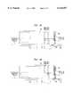
- FIG. 2Aillustrates an elevational side view of an electronics case mounted on a supporting substrate with a cutout view of the electrically conductive pin secured to the supporting substrate by a force-fit collar with a knurled end;
- FIG. 2Billustrates an elevational side view of an electronics case mounted on a supporting substrate with a cutout view of the electrically conductive pin secured to the supporting substrate by a collar that has a snap-in feature at the end of the pin;
- FIG. 3is a flow diagram of a method of manufacturing an embodiment of an electronics case constructed in accordance with the principles of the present invention.
- the electronics case 110is an enclosure containing various electronic components that make up an electronic circuit and is formed from a metal substrate.
- the case 110usually only has a top 111 and one to four sidewalls and may not have a bottom surface.
- the bottom surface of the case 110may be an encapsulant that surrounds the components in the case 110.
- the inner surface of the metal substrate making up the sides and top 111 of the case 110is lined with a dielectric material (not shown) that insulates the metal substrate from electronic components located within the case 110.
- the metal substrate and dielectric material liningcan also serve as a printed wiring or circuit board for the electronic components contained therein by locating electrically conductive traces thereon.
- the case 110 enclosureis a reservoir that receives a separate circuit board 140 therein that may include some or all of the electronic components of a circuit.
- the circuit board 140can be placed inside the case 110 by either compression fitting it therein or using other methods familiar to those skilled in the art.
- the electrical pins 122Extending from the bottom of the case 110 are electrical pins 122 to provide electrical connectivity between the circuit and components within the case 110 and the electronic circuit associated with the supporting substrate 120 upon which the case 110 is mounted.
- the electrical pins 122extend from the bottom of a circuit board 140 that is mounted within the case 110.
- apertures 121On the surface of the supporting substrate 120 are apertures 121 to receive the electrical pins 122 and complete the electrical connection.
- a mountable case 110permits a manufacturer to use off-the-shelf preassembled cased circuits to assemble and manufacture electronic systems.
- the electronic components and circuitry contained within the case 110cooperate to yield a modular power converter (or "board-mountable power supply").
- a mountable case 110 of this typeprovides an advantageous method for manufacturers to use electronic circuits of wide application that can be largely standardized, such as converters and other power circuits, in the assembly of larger electronic systems.
- the circuit and components contained in the case 110are held in place by an encapsulant, such as epoxy or some other dielectric polymers.
- the encapsulantoccupies at least part of the case 110 enclosure and may actually be the surface that is in direct contact with a supporting substrate 120 when the case 110 is mounted.
- the encapsulantwhile not necessary in some embodiments of the present invention, provides support for electronic components within the case 110 and rigidity to the case 110 as a whole.
- a power supply and method of manufacture of a mountable case 110 of this typeis described in Stevens, et. al., U.S. Pat. No. 5,835,350, entitled “Encapsulated, Board-Mountable Power Supply and Method of Manufacture Therefor," which is incorporated herein by this reference thereto.
- each aperture 112Inserted through each aperture 112 is an electrically conductive pin 130, one end of which has a collar 132 that locks into an electrically conductive pin aperture 131 on the supporting substrate 120 circuit board that, in most cases, has electrically conductive traces located thereon.
- the electrically conductive pin 130passes through the aperture 112 and interior of the case 110, to emerge from the enclosure formed by the case 110 at a point opposite the top surface 111.
- the pin 130functions both as a heat sink mount for the case 110 and as a case ground pin for the substrate that forms the case 110 sidewalls and top 111.
- the heat sink 1have a hollow shank to receive fasteners for mounting a heat sink over the case 110.
- the heat sinkcan be fastened to the pins 130 by using self-threading fasteners, or the hollow shanks of the pins 130 can be prethreaded to receive screws, bolts or mounting posts extending from the heat sink.
- FIG. 2Aillustrated is an elevational side view of an electronics case 110 mounted on a supporting substrate 120.
- the partial cutout on the side of the case 110illustrates the electrically conductive pin 130 passing through the enclosure formed by the case 110.
- the pin 130also passes through a printed circuit board 140 mounted inside the case 110.
- the end of the pin 130 emerging from the case 110 enclosureis inserted into an electrically conductive pin aperture 131 on the supporting substrate 120.
- the ground connectionto improve electromagnetic interference control.
- the collar 132 on the illustrated pin 130is knurled so that it can be force-fit into the supporting substrate 120 and lock itself into place.
- FIG. 2Billustrates a collar 132 that has a snap-in feature to lock the pin 130 to the supporting substrate 120 and make the case ground connection.
- soldercovers one end of the pin 130.
- FIG. 3illustrated is a flow diagram of one embodiment of a method of manufacturing an electronics case according to the principles of the present invention.
- the methodbegins at a start step 310.
- the next stepis folding a metal substrate to form the sidewalls and top of an enclosure having a reservoir therein during a construct case step 320.
- the peripheral sidewallsmay be sealed through several methods such as, without limitation, applying an adhesive, applying an interference-fit plastic insert, welding the corners of the sidewalls, or soldering the interior corners to provide a solderable pattern on an interior layer of the case. Regardless of the selected method, if an encapsulant is to placed in the case, the corners should be meticulously sealed to prevent escape of the encapsulant while placing the encapsulant within the case or during curing of the encapsulant.
- the next stepis to form an aperture on a major surface of the case in a form aperture step 330.
- the apertureis formed to receive an electrically conductive pin passing through the aperture the interior enclosure of the case to emerge from the enclosure opposite the major surface.
- a dielectric materialis then deposited on the inner surfaces of the case sidewalls during a deposit dielectric material step 340.
- the dielectric materialprovides insulation for electronic components located within the case.
- dielectric materialis deposited on the substrate before the construct case step 320.
- a plurality of electrically conductive tracesare located on the dielectric material, which electrically conductive traces are insulated from the metal substrate. The electrically conductive traces are placed on the dielectric material at such time, or times, as those skilled in the art determine.
- An electrically conductive pinis then inserted through the aperture and the interior of the case to emerge from the case opposite the aperture in an insert conductive pin step 350.
- any number of aperturescan be provided during the form aperture step 330 and any number of electrically conductive pins can be inserted during the insert conductive pin step 350 and still be within the scope of the invention.
- manufacturing embodiment steps within the scope of the present inventioninclude a step to install the electronic components of a power converter (not shown) and at least partially filling the enclosure with an encapsulant (not shown), which steps occur at such time as those skilled in the art may determine. If an encapsulant is used to partially fill the enclosure, environmental protection (e.g., protection from dirt and moisture) for the electronic components located within the case is provided.
- the manufacturing methodconcludes at a end step 360.
- the completed casewhich may be a power converter, can then be coupled to a printed wiring or circuit supporting substrate using any number of techniques including, without limitation, through hole attachment, surface mounting, connector attachment or mechanical piece part attachment (e.g., compression mounting).
- a printed wiring or circuit supporting substrateusing any number of techniques including, without limitation, through hole attachment, surface mounting, connector attachment or mechanical piece part attachment (e.g., compression mounting).
- the end of The electrically conductive pinis covered with solder.
- An electronics caseis constructed according to the principles of the present invention as described with respect to the preceding FIGURES.
- the aforementioned electronics case and method of manufacturingare submitted for illustrative purposes only.
- Other case embodiments and alternative methods of manufacturing in accordance with the general principles, as submitted herein,are well within the broad scope of the present invention.
Landscapes
- Engineering & Computer Science (AREA)
- Microelectronics & Electronic Packaging (AREA)
- Casings For Electric Apparatus (AREA)
Abstract
Description
Claims (12)
Priority Applications (1)
| Application Number | Priority Date | Filing Date | Title |
|---|---|---|---|
| US09/289,686US6144557A (en) | 1999-04-09 | 1999-04-09 | Self-locking conductive pin for printed wiring substrate electronics case |
Applications Claiming Priority (1)
| Application Number | Priority Date | Filing Date | Title |
|---|---|---|---|
| US09/289,686US6144557A (en) | 1999-04-09 | 1999-04-09 | Self-locking conductive pin for printed wiring substrate electronics case |
Publications (1)
| Publication Number | Publication Date |
|---|---|
| US6144557Atrue US6144557A (en) | 2000-11-07 |
Family
ID=23112637
Family Applications (1)
| Application Number | Title | Priority Date | Filing Date |
|---|---|---|---|
| US09/289,686Expired - LifetimeUS6144557A (en) | 1999-04-09 | 1999-04-09 | Self-locking conductive pin for printed wiring substrate electronics case |
Country Status (1)
| Country | Link |
|---|---|
| US (1) | US6144557A (en) |
Cited By (32)
| Publication number | Priority date | Publication date | Assignee | Title |
|---|---|---|---|---|
| USD464317S1 (en) | 2002-03-22 | 2002-10-15 | Densei-Lambda Kabushiki Kaisha | Power supply |
| USD465199S1 (en) | 2002-03-22 | 2002-11-05 | Densei-Lambda Kabushiki Kaisha | Power supply |
| US6499215B1 (en) | 2000-06-29 | 2002-12-31 | International Business Machines Corporation | Processing of circuit boards with protective, adhesive-less covers on area array bonding sites |
| WO2002058138A3 (en)* | 2000-12-05 | 2003-01-23 | Intel Corp | An electronic assembly having a heat pipe that conducts heat from a semiconductor die |
| US6560110B1 (en)* | 2002-02-22 | 2003-05-06 | Delphi Technologies, Inc. | Corrosive resistant flip chip thermal management structure |
| USD475012S1 (en) | 2001-06-19 | 2003-05-27 | Kabushiki Kaisha Toshiba | Portion of a power converter |
| USD476622S1 (en) | 2001-06-19 | 2003-07-01 | Kabushiki Kaisha Toshiba | Portion of a power converter |
| US20040257786A1 (en)* | 2003-06-05 | 2004-12-23 | Osamu Murasawa | Electronic device, information processor, and electromagnetic radiation suppressing member |
| US6881894B2 (en)* | 2000-10-13 | 2005-04-19 | Nec Lcd Technologies, Ltd. | EMI shielding structures |
| US20060262512A1 (en)* | 2005-05-17 | 2006-11-23 | Klein Robert D | Modular electronics enclosure |
| US20080037238A1 (en)* | 2004-03-17 | 2008-02-14 | Mitsubishi Denki Kabushiki Kaisha | Structure for electromagnetically shielding a substrate |
| US20080174984A1 (en)* | 2007-01-24 | 2008-07-24 | Mitsumi Electric Co. Ltd. | High frequency tuner module |
| US20080251893A1 (en)* | 2007-04-16 | 2008-10-16 | English Gerald R | Mounting clips for use with electromagnetic interference shielding and methods of using the same |
| US20090046438A1 (en)* | 2007-08-07 | 2009-02-19 | Shinichi Maeda | Attachment structure of an attached-plate of a substrate |
| EP2059108A2 (en)* | 2007-11-08 | 2009-05-13 | Delphi Technologies, Inc. | A conductive elastomeric shielding device and method of forming same |
| US20090161318A1 (en)* | 2007-12-19 | 2009-06-25 | Dialogic Corporation | Thermal management systems and methods |
| US20100079963A1 (en)* | 2008-09-29 | 2010-04-01 | Murata Manufacturing Co., Ltd. | Circuit module |
| US20100091462A1 (en)* | 2007-02-15 | 2010-04-15 | Nec Corporation | Electronic device-mounted apparatus and noise suppression method for same |
| US20100270068A1 (en)* | 2007-11-12 | 2010-10-28 | Kim Suan Pang | Tuner housing |
| US20100323540A1 (en)* | 2009-06-19 | 2010-12-23 | Leviton Manufacturing Company, Inc. | Mehtod and apparatus for grounding and mounting a high amperage single pole connector |
| US20110255250A1 (en)* | 2010-04-19 | 2011-10-20 | Richard Hung Minh Dinh | Printed circuit board components for electronic devices |
| US20130342007A1 (en)* | 2012-06-21 | 2013-12-26 | Lear Corporation | Electrical connector |
| US20150146375A1 (en)* | 2013-11-26 | 2015-05-28 | Delta Electronics (Shanghai) Co., Ltd. | Power conversion device and power conversion assembly |
| USD794034S1 (en)* | 2009-01-07 | 2017-08-08 | Samsung Electronics Co., Ltd. | Memory device |
| USD794643S1 (en)* | 2009-01-07 | 2017-08-15 | Samsung Electronics Co., Ltd. | Memory device |
| USD794644S1 (en)* | 2009-01-07 | 2017-08-15 | Samsung Electronics Co., Ltd. | Memory device |
| USD794641S1 (en)* | 2009-01-07 | 2017-08-15 | Samsung Electronics Co., Ltd. | Memory device |
| USD794642S1 (en)* | 2009-01-07 | 2017-08-15 | Samsung Electronics Co., Ltd. | Memory device |
| USD795262S1 (en)* | 2009-01-07 | 2017-08-22 | Samsung Electronics Co., Ltd. | Memory device |
| USD795261S1 (en)* | 2009-01-07 | 2017-08-22 | Samsung Electronics Co., Ltd. | Memory device |
| TWI760062B (en)* | 2020-05-14 | 2022-04-01 | 家登精密工業股份有限公司 | Reticle pod provided with holding pins and method for holding reticle |
| US11303064B2 (en)* | 2020-07-10 | 2022-04-12 | Beijing Voyager Technology Co., Ltd. | Methods and apparatuses for aligning and coupling a circuit board with a chassis and another circuit board |
Citations (8)
| Publication number | Priority date | Publication date | Assignee | Title |
|---|---|---|---|---|
| US4325103A (en)* | 1978-12-28 | 1982-04-13 | Murata Manufacturing Co., Ltd. | Provisional fixing structure of electronic tuner |
| US4502098A (en)* | 1981-02-10 | 1985-02-26 | Brown David F | Circuit assembly |
| US4599680A (en)* | 1983-09-26 | 1986-07-08 | Southwest Research Institute | Packaging arrangement for spacecraft computer |
| US5835350A (en)* | 1996-12-23 | 1998-11-10 | Lucent Technologies Inc. | Encapsulated, board-mountable power supply and method of manufacture therefor |
| US5901040A (en)* | 1997-07-30 | 1999-05-04 | Hewlett-Packard Company | Heat sink and Faraday Cage assembly for a semiconductor module and a power converter |
| US5905622A (en)* | 1998-03-23 | 1999-05-18 | Pass & Seymour, Inc. | Transient voltage surge suppressor with internal barriers |
| US5907478A (en)* | 1996-12-25 | 1999-05-25 | Alps Electric Co., Ltd. | Unit part mounting structure |
| US6031732A (en)* | 1994-11-28 | 2000-02-29 | Kabushiki Kaisha Toshiba | Electronic apparatus with a shield structure and a shield case used in the shield structure and a manufacturing method of the shield case |
- 1999
- 1999-04-09USUS09/289,686patent/US6144557A/ennot_activeExpired - Lifetime
Patent Citations (8)
| Publication number | Priority date | Publication date | Assignee | Title |
|---|---|---|---|---|
| US4325103A (en)* | 1978-12-28 | 1982-04-13 | Murata Manufacturing Co., Ltd. | Provisional fixing structure of electronic tuner |
| US4502098A (en)* | 1981-02-10 | 1985-02-26 | Brown David F | Circuit assembly |
| US4599680A (en)* | 1983-09-26 | 1986-07-08 | Southwest Research Institute | Packaging arrangement for spacecraft computer |
| US6031732A (en)* | 1994-11-28 | 2000-02-29 | Kabushiki Kaisha Toshiba | Electronic apparatus with a shield structure and a shield case used in the shield structure and a manufacturing method of the shield case |
| US5835350A (en)* | 1996-12-23 | 1998-11-10 | Lucent Technologies Inc. | Encapsulated, board-mountable power supply and method of manufacture therefor |
| US5907478A (en)* | 1996-12-25 | 1999-05-25 | Alps Electric Co., Ltd. | Unit part mounting structure |
| US5901040A (en)* | 1997-07-30 | 1999-05-04 | Hewlett-Packard Company | Heat sink and Faraday Cage assembly for a semiconductor module and a power converter |
| US5905622A (en)* | 1998-03-23 | 1999-05-18 | Pass & Seymour, Inc. | Transient voltage surge suppressor with internal barriers |
Cited By (50)
| Publication number | Priority date | Publication date | Assignee | Title |
|---|---|---|---|---|
| US6700068B2 (en)* | 2000-06-29 | 2004-03-02 | International Business Machines Corporation | Adhesive-less cover on area array bonding site of circuit board |
| US6499215B1 (en) | 2000-06-29 | 2002-12-31 | International Business Machines Corporation | Processing of circuit boards with protective, adhesive-less covers on area array bonding sites |
| US6881894B2 (en)* | 2000-10-13 | 2005-04-19 | Nec Lcd Technologies, Ltd. | EMI shielding structures |
| US6535386B2 (en)* | 2000-12-05 | 2003-03-18 | Intel Corporation | Electronic assembly having a heat pipe that conducts heat from a semiconductor die |
| WO2002058138A3 (en)* | 2000-12-05 | 2003-01-23 | Intel Corp | An electronic assembly having a heat pipe that conducts heat from a semiconductor die |
| USD475012S1 (en) | 2001-06-19 | 2003-05-27 | Kabushiki Kaisha Toshiba | Portion of a power converter |
| USD476622S1 (en) | 2001-06-19 | 2003-07-01 | Kabushiki Kaisha Toshiba | Portion of a power converter |
| US6560110B1 (en)* | 2002-02-22 | 2003-05-06 | Delphi Technologies, Inc. | Corrosive resistant flip chip thermal management structure |
| USD465199S1 (en) | 2002-03-22 | 2002-11-05 | Densei-Lambda Kabushiki Kaisha | Power supply |
| USD464317S1 (en) | 2002-03-22 | 2002-10-15 | Densei-Lambda Kabushiki Kaisha | Power supply |
| US20040257786A1 (en)* | 2003-06-05 | 2004-12-23 | Osamu Murasawa | Electronic device, information processor, and electromagnetic radiation suppressing member |
| US7053295B2 (en)* | 2003-06-05 | 2006-05-30 | Sony Computer Entertainment, Inc. | Electronic device, information processor, and electromagnetic radiation suppressing member |
| US20080037238A1 (en)* | 2004-03-17 | 2008-02-14 | Mitsubishi Denki Kabushiki Kaisha | Structure for electromagnetically shielding a substrate |
| US20060262512A1 (en)* | 2005-05-17 | 2006-11-23 | Klein Robert D | Modular electronics enclosure |
| US7245497B2 (en) | 2005-05-17 | 2007-07-17 | Itt Manufacturing Enterprises, Inc. | Modular electronics enclosure |
| US20080174984A1 (en)* | 2007-01-24 | 2008-07-24 | Mitsumi Electric Co. Ltd. | High frequency tuner module |
| US7764513B2 (en)* | 2007-01-24 | 2010-07-27 | Mitsumi Electric Co., Ltd. | High frequency tuner module |
| US20100091462A1 (en)* | 2007-02-15 | 2010-04-15 | Nec Corporation | Electronic device-mounted apparatus and noise suppression method for same |
| US20080251893A1 (en)* | 2007-04-16 | 2008-10-16 | English Gerald R | Mounting clips for use with electromagnetic interference shielding and methods of using the same |
| US7501587B2 (en)* | 2007-04-16 | 2009-03-10 | Laird Technologies, Inc. | Mounting clips for use with electromagnetic interference shielding and methods of using the same |
| US20090046438A1 (en)* | 2007-08-07 | 2009-02-19 | Shinichi Maeda | Attachment structure of an attached-plate of a substrate |
| US8351211B2 (en)* | 2007-08-07 | 2013-01-08 | Panasonic Corporation | Attachment structure of an attached-plate of a substrate |
| EP2059108A2 (en)* | 2007-11-08 | 2009-05-13 | Delphi Technologies, Inc. | A conductive elastomeric shielding device and method of forming same |
| US20090122507A1 (en)* | 2007-11-08 | 2009-05-14 | Snider Chris R | Conductive elastomeric shielding device and method of forming same |
| US7609530B2 (en)* | 2007-11-08 | 2009-10-27 | Delphi Technologies, Inc. | Conductive elastomeric shielding device and method of forming same |
| US8242361B2 (en)* | 2007-11-12 | 2012-08-14 | Thomson Licensing | Tuner housing |
| US20100270068A1 (en)* | 2007-11-12 | 2010-10-28 | Kim Suan Pang | Tuner housing |
| US20090161318A1 (en)* | 2007-12-19 | 2009-06-25 | Dialogic Corporation | Thermal management systems and methods |
| US20100079963A1 (en)* | 2008-09-29 | 2010-04-01 | Murata Manufacturing Co., Ltd. | Circuit module |
| US7924571B2 (en)* | 2008-09-29 | 2011-04-12 | Murata Manufacturing Co., Ltd. | Circuit module |
| USD794644S1 (en)* | 2009-01-07 | 2017-08-15 | Samsung Electronics Co., Ltd. | Memory device |
| USD794643S1 (en)* | 2009-01-07 | 2017-08-15 | Samsung Electronics Co., Ltd. | Memory device |
| USD795261S1 (en)* | 2009-01-07 | 2017-08-22 | Samsung Electronics Co., Ltd. | Memory device |
| USD795262S1 (en)* | 2009-01-07 | 2017-08-22 | Samsung Electronics Co., Ltd. | Memory device |
| USD794642S1 (en)* | 2009-01-07 | 2017-08-15 | Samsung Electronics Co., Ltd. | Memory device |
| USD794641S1 (en)* | 2009-01-07 | 2017-08-15 | Samsung Electronics Co., Ltd. | Memory device |
| USD794034S1 (en)* | 2009-01-07 | 2017-08-08 | Samsung Electronics Co., Ltd. | Memory device |
| US7967615B2 (en)* | 2009-06-19 | 2011-06-28 | Leviton Manufacturing Company, Inc. | Method and apparatus for grounding and mounting a high amperage single pole connector |
| US20100323540A1 (en)* | 2009-06-19 | 2010-12-23 | Leviton Manufacturing Company, Inc. | Mehtod and apparatus for grounding and mounting a high amperage single pole connector |
| US20110255250A1 (en)* | 2010-04-19 | 2011-10-20 | Richard Hung Minh Dinh | Printed circuit board components for electronic devices |
| US20110255850A1 (en)* | 2010-04-19 | 2011-10-20 | Richard Hung Minh Dinh | Electronic subassemblies for electronic devices |
| CN103515728A (en)* | 2012-06-21 | 2014-01-15 | 李尔公司 | Electrical connector |
| CN103515728B (en)* | 2012-06-21 | 2015-12-02 | 李尔公司 | Electric connector |
| US8777642B2 (en)* | 2012-06-21 | 2014-07-15 | Lear Corporation | Electrical connector |
| US20130342007A1 (en)* | 2012-06-21 | 2013-12-26 | Lear Corporation | Electrical connector |
| US9414480B2 (en)* | 2013-11-26 | 2016-08-09 | Delta Electronics (Shanghai) Co., Ltd. | Power conversion device and power conversion assembly |
| US20150146375A1 (en)* | 2013-11-26 | 2015-05-28 | Delta Electronics (Shanghai) Co., Ltd. | Power conversion device and power conversion assembly |
| TWI760062B (en)* | 2020-05-14 | 2022-04-01 | 家登精密工業股份有限公司 | Reticle pod provided with holding pins and method for holding reticle |
| US11303064B2 (en)* | 2020-07-10 | 2022-04-12 | Beijing Voyager Technology Co., Ltd. | Methods and apparatuses for aligning and coupling a circuit board with a chassis and another circuit board |
| US20220209462A1 (en)* | 2020-07-10 | 2022-06-30 | Beijing Voyager Technology Co., Ltd. | Methods and apparatuses for aligning and coupling a circuit board with a chassis and another circuit board |
Similar Documents
| Publication | Publication Date | Title |
|---|---|---|
| US6144557A (en) | Self-locking conductive pin for printed wiring substrate electronics case | |
| US6421244B1 (en) | Power module | |
| US5926373A (en) | Encapsulated, board-mountable power supply and method of manufacture | |
| KR101203466B1 (en) | Power system module and method for fabricating the same | |
| US5144946A (en) | Combined pacemaker substrate and electrical interconnect and method of assembly | |
| US6373714B1 (en) | Surface mounting part | |
| US5959842A (en) | Surface mount power supply package and method of manufacture thereof | |
| KR19990029590A (en) | Vertical interconnect package based on lead frame and manufacturing method thereof | |
| JP4437860B2 (en) | Wiring block storage structure | |
| JPH07153907A (en) | Power semiconductor module | |
| US6320762B1 (en) | Fixed conductive pin for printed wiring substrate electronics case and method of manufacture therefor | |
| JP3842010B2 (en) | Electronic equipment having multiple substrates | |
| JPH05327249A (en) | Electronic circuit module and manufacture thereof | |
| US20020005579A1 (en) | Semiconductor apparatus and frame used for fabricating the same | |
| JP2736165B2 (en) | Hybrid circuit device | |
| JPH09246433A (en) | Radiation structure of module | |
| JP2612455B2 (en) | Substrate for mounting semiconductor elements | |
| JPH06125191A (en) | Shield part | |
| JP2538636B2 (en) | Semiconductor device | |
| KR100284661B1 (en) | Modular structure power circuit device | |
| JPH0451486Y2 (en) | ||
| JPH037985Y2 (en) | ||
| JPH06163810A (en) | Lead block for surface packaging hybrid ic | |
| JP2858252B2 (en) | Electrode structure of electronic components for surface mounting | |
| JPH0458189B2 (en) |
Legal Events
| Date | Code | Title | Description |
|---|---|---|---|
| AS | Assignment | Owner name:LUCENT TECHNOLOGIES INC., NEW JERSEY Free format text:ASSIGNMENT OF ASSIGNORS INTEREST;ASSIGNORS:CHEN, SHIAW-JONG S.;HOOEY, ROGER J.;REEL/FRAME:010002/0669 Effective date:19990517 | |
| STCF | Information on status: patent grant | Free format text:PATENTED CASE | |
| FPAY | Fee payment | Year of fee payment:4 | |
| AS | Assignment | Owner name:TYCO ELECTRONICS LOGISTICS A.G., SWITZERLAND Free format text:ASSIGNMENT OF ASSIGNORS INTEREST;ASSIGNOR:LUCENT TECHNOLOGIES INC.;REEL/FRAME:020103/0664 Effective date:20001229 | |
| AS | Assignment | Owner name:LINEAGE OVERSEAS CORP., DELAWARE Free format text:ASSIGNMENT OF ASSIGNORS INTEREST;ASSIGNOR:TYCO ELECTRONICS LOGISTICS AG;REEL/FRAME:020609/0580 Effective date:20080228 Owner name:LINEAGE POWER CORPORATION, TEXAS Free format text:ASSIGNMENT OF ASSIGNORS INTEREST;ASSIGNOR:LINEAGE OVERSEAS CORP.;REEL/FRAME:020582/0184 Effective date:20080228 | |
| FPAY | Fee payment | Year of fee payment:8 | |
| AS | Assignment | Owner name:WELLS FARGO FOOTHILL, LLC, AS AGENT, CALIFORNIA Free format text:SECURITY AGREEMENT;ASSIGNOR:LINEAGE POWER CORPORATION;REEL/FRAME:021876/0066 Effective date:20081121 Owner name:WELLS FARGO FOOTHILL, LLC, AS AGENT,CALIFORNIA Free format text:SECURITY AGREEMENT;ASSIGNOR:LINEAGE POWER CORPORATION;REEL/FRAME:021876/0066 Effective date:20081121 | |
| AS | Assignment | Owner name:LINEAGE POWER CORPORATION, TEXAS Free format text:PATENT RELEASE AND REASSIGNMENT;ASSIGNOR:WELLS FARGO CAPITAL FINANCE, LLC;REEL/FRAME:027934/0566 Effective date:20110228 | |
| FPAY | Fee payment | Year of fee payment:12 | |
| AS | Assignment | Owner name:GE POWER ELECTRONICS, INC., TEXAS Free format text:CHANGE OF NAME;ASSIGNOR:LINEAGE POWER CORPORATION;REEL/FRAME:045581/0581 Effective date:20120101 | |
| AS | Assignment | Owner name:ABB SCHWEIZ AG, SWITZERLAND Free format text:ASSIGNMENT OF ASSIGNORS INTEREST;ASSIGNOR:GE POWER ELECTRONICS, INC.;REEL/FRAME:050207/0076 Effective date:20180813 | |
| AS | Assignment | Owner name:ABB POWER ELECTRONICS INC., TEXAS Free format text:ASSIGNMENT OF ASSIGNORS INTEREST;ASSIGNOR:ABB SCHWEIZ AG;REEL/FRAME:052430/0136 Effective date:20200207 |