US6144481A - Method and system for actuating electro-mechanical ribbon elements in accordance to a data stream - Google Patents
Method and system for actuating electro-mechanical ribbon elements in accordance to a data streamDownload PDFInfo
- Publication number
- US6144481A US6144481AUS09/215,106US21510698AUS6144481AUS 6144481 AUS6144481 AUS 6144481AUS 21510698 AUS21510698 AUS 21510698AUS 6144481 AUS6144481 AUS 6144481A
- Authority
- US
- United States
- Prior art keywords
- data stream
- conductive layer
- voltage
- modulated
- bipolar
- Prior art date
- Legal status (The legal status is an assumption and is not a legal conclusion. Google has not performed a legal analysis and makes no representation as to the accuracy of the status listed.)
- Expired - Lifetime
Links
Images


Classifications
- G—PHYSICS
- G02—OPTICS
- G02B—OPTICAL ELEMENTS, SYSTEMS OR APPARATUS
- G02B26/00—Optical devices or arrangements for the control of light using movable or deformable optical elements
- G02B26/08—Optical devices or arrangements for the control of light using movable or deformable optical elements for controlling the direction of light
- G02B26/0808—Optical devices or arrangements for the control of light using movable or deformable optical elements for controlling the direction of light by means of one or more diffracting elements
- G—PHYSICS
- G02—OPTICS
- G02B—OPTICAL ELEMENTS, SYSTEMS OR APPARATUS
- G02B5/00—Optical elements other than lenses
- G02B5/18—Diffraction gratings
- G02B5/1828—Diffraction gratings having means for producing variable diffraction
- H—ELECTRICITY
- H04—ELECTRIC COMMUNICATION TECHNIQUE
- H04N—PICTORIAL COMMUNICATION, e.g. TELEVISION
- H04N5/00—Details of television systems
- H04N5/74—Projection arrangements for image reproduction, e.g. using eidophor
- H04N5/7416—Projection arrangements for image reproduction, e.g. using eidophor involving the use of a spatial light modulator, e.g. a light valve, controlled by a video signal
Definitions
- This inventionrelates to a method and a system for actuating electromechanical ribbon elements of a Grating Light Valve (GLV) in accordance to a data stream. More particularly the invention relates to a method and system which is able to prevent a charge accumulation in the dielectric elements of the GLV.
- GLVGrating Light Valve
- Electro-mechanical spatial light modulatorshave been designed for a variety of applications, including image processing, display, optical computing and printing.
- Optical beam processing for printing with deformable mirrorshas been described by L. J. Hornbeck; see U.S. Pat. No. 4,596,992, issued Jun. 24, 1984, entitled “Linear Spatial Light Modulator and Printer”.
- a device for optical beam modulation using cantilever mechanical beamshas also been disclosed; see U.S. Pat. No. 4,492,435, issued Jan. 8, 1985 to M. E. Banton, entitled “Multiple Array Full Width Electro-Mechanical Modulator," and U.S. Pat. No. 5,661,593, issued Aug. 26, 1997 to C. D. Engle, entitled “Linear Electrostatic Modulator”.
- electromechanical gratingsinclude wavelength division multiplexing and spectrometers; see U.S. Pat. No. 5,757,536, issued May 26, 1998 to A. J. Ricco et al., entitled “Electrically Programmable Diffraction Grating”.
- Electro-mechanical gratingsare well known in the patent literature; see U.S. Pat. No. 4,011,009, issued Mar. 8, 1977 to W. L. Lama et al., entitled “Reflection Diffraction Grating Having a Controllable Blaze Angle," and U.S. Pat. No. 5,115,344, issued May 19, 1992 to J. E. Jaskie, entitled “Tunable Diffraction Grating”. More recently, Bloom et al. described an apparatus and method of fabrication for a device for optical beam modulation, known to one skilled in the art as a grating-light valve (GLV); see U.S. Pat. No. 5,311,360, issued May 10, 1994, entitled “Method and Apparatus for Modulating a Light Beam”.
- GLVgrating-light valve
- an attractive electrostatic forceis produced by a single polarity voltage difference between the ground plane and the conducting layer atop the ribbon layer.
- This attractive forcechanges the heights of the ribbons relative to the substrate.
- modulating the voltage waveformit is possible to modulate the diffracted optical beam as needed.
- a single polarity voltage waveformcan lead to device operation difficulties if charge build-up occurs on the intermediate dielectric layers between the ground plane and the conductor on the ribbons. If this dielectric charge does not dissipate quickly enough after the actuation voltage is turned off, a significant charge accumulation can occur that leads to deterioration in the performance of the device with repetitive actuation.
- charge injection and trapping into insulating dielectric films, such as silicon nitride and silicon dioxide, on semiconductorsis well known to occur in various microelectronic devices. Charging effects in silicon dioxide can be minimized by proper deposition, as described, for example, in “Charge transport and transport phenomena in off-stoichiometric silicon dioxide films," Journal of Applied Physics, 54, 1983, pp. 5801-5827, by D. J. Maria et al.
- charge injection into silicon nitridecan be used beneficially in non-volatile memories such as the device described by R. T. Bate; see U.S. Pat. No. 4,360,900, issued Nov. 23, 1982, entitled "Non-Volatile Semiconductor Memory Elements".
- This objectis achieved with a method for actuating electro-mechanical ribbon elements suspended over a channel defining a bottom surface and having a bottom conductive layer formed below said bottom surface.
- the methodcomprises the steps of:
- Another objectis to provide a system for actuating electro-mechanical grating elements wherein the inventive system minimizes charge accumulation in the dielectric layers of the grating elements. Additionally, stable device operation should be achieved in accordance with the inventive system.
- This objectis achieved with a system for actuating electro-mechanical ribbon elements suspended over a channel defining a bottom surface and having a bottom conductive layer formed below said bottom surface.
- the systemcomprises:
- a modulatorfor generating from said data stream a modulated bipolar voltage signal whose time average is equal to the time average of a bias voltage applied to the bottom conductive layer.
- the above objectis also achieved by a system for actuating electro-mechanical ribbon elements suspended over a channel defining a bottom surface and having a bottom conductive layer formed below said bottom surface.
- the systemcomprises:
- a data generatorfor providing a data stream
- a modulatorfor generating from the data stream a modulated bipolar voltage signal controlled by said polarity control counter.
- An advantage of the inventive method and the systemis the use of a DC-free bipolar waveform to actuate the GLV device ribbon elements.
- the DC-free waveformproduces nearly the same temporal modulation of the diffracted optical beam as the corresponding single polarity waveform while minimizing charge accumulation in the dielectric layers of the electromechanical grating device located between the ribbon layer conductor and the conducting plane of the substrate.
- the accumulated charge on the dielectricsresults in a ribbon response that varies after multiple actuations, leading to an undesirable temporal variation in the diffracted optical beam and, in certain cases, to complete failure of a ribbon element through stiction.
- a DC-free bipolar voltage waveformminimizes charge accumulation, thus leading to a stable ribbon response.
- FIGS. 1a-1bis an illustration of light diffraction by a bi-level electro-mechanical grating device in the un-actuated and actuated state respectively;
- FIG. 2is a view perpendicular to the illustration of FIG. 1 showing a suspended un-actuated ribbon element above the channel and with supporting layers;
- FIG. 3is an illustration of unipolar voltage waveforms for actuating the ribbon elements to generate pulse width modulated light
- FIGS. 4a-4bshow the change in ribbon behavior due to charging with actuation by a unipolar triangular waveform
- FIGS. 5a-5bshow a stable behavior of the ribbon elements actuated by a bipolar triangular waveform
- FIG. 6is an illustration of a bipolar voltage waveform for actuating the ribbon elements to generate pulse width modulated light
- FIG. 7is an illustration of an alternate bipolar voltage waveform for actuating the ribbon elements to generate pulse width modulated light
- FIG. 8is a block diagram of a circuit that generates a bipolar voltage waveform for pulse width modulated light
- FIG. 9is an illustration of a bipolar voltage waveform for actuating the ribbons to generate pulse amplitude modulated light.
- FIG. 10is a block diagram of a circuit that generates a bipolar voltage waveform with a less frequent change in polarity
- FIG. 11is an illustration of an alternate voltage waveform for actuating the ribbon elements to generate pulse width modulated light wherein the bias voltage on the bottom conductive layer is time varying;
- FIG. 12is a block diagram of a circuit that generates a bipolar voltage waveform for actuating the ribbon elements to generate pulse width modulated light.
- FIGS. 1a, 1b and 2The structure of a typical Grating Light Valve (GLV) device is shown in FIGS. 1a, 1b and 2.
- FIG. 1adepicts the ribbon structure of the device in the unactuated state and FIG. 1b in the actuated state.
- FIG. 2is the view of the same device (as shown in FIG. 1a) in the unactuated state but rotated 90 degrees to provide an insight into the layer build-up of the GLV.
- a substrate 20is provided which may be single crystal silicon or glass.
- a bottom conductive layer 22is generated by ion implantation near the surface 23 of the substrate 20.
- the increased conductivityis achieved by the application of a bottom conductive layer 22 on top of the glass substrate 20.
- the conductive layer 22is covered by a protective layer 24, which is for example of thermal oxide.
- a dielectric spacer layer 26is formed atop the protective layer 24 and contains a channel 28 where the active region of the GLV device is located. The channel 28 defines a depth which is governed by the deposited thickness of the spacer layer 26.
- the spacer layer 26defines an upper surface level 27.
- a plurality of ribbon elements 31is patterned from a ribbon layer 30 formed atop the spacer layer 26.
- the ribbon layer 30comprises a dielectric material, which may be of silicon nitride, covered by a conductive and reflective layer 32.
- the conductive and reflective layer 32 of every other ribbon element 31is connected to the bottom conductive layer 22 through an opening 34 that is filled with a thick layer of conducting martial 36.
- the thickness and tensile stress of the ribbon layer 30is chosen to optimize performance by influencing the electrostatic force required for actuation and the returning force, which affects the speed, resonance frequency and voltage requirements of the ribbon elements 31 of the GLV.
- an attractive electrostatic forceis produced by a voltage difference between the bottom conductive layer 22 and the reflective and conductive layer 32 atop the ribbon layer 30.
- the unactuated statesee FIG. 1a
- all of the ribbon elements 31 in the GLV deviceare suspended above the substrate 20 at the same height.
- an incident light beam 14is primarily reflected as from a mirror to form a reflected light beam 15.
- a voltageis applied to every other ribbon element producing a grating (see FIG. 1a).
- every other ribbon elementis in contact with the protective layer 24.
- the light beamis primarily diffracted into a 1st order 17 and a-1 st order 18.
- One or both of these diffracted orderscan be collected and used by an optical system (not shown), depending on the application.
- the applied voltageis removed, the force due to the tensile stress restores the ribbon elements 31 to their original un-actuated state (see FIG. 1a).
- the intensity of the diffracted orderscan be varied by modulating the voltage waveform applied to the ribbon elements 31.
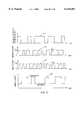
- FIG. 3illustrates modulation of the ribbon element voltage 52 with a positive polarity waveform to change the ribbon height 54 so as to obtain the pulse width modulation of a diffracted light intensity 50.
- An inverted ribbon element voltage waveform 56 with negative polaritycan also produce the same variation in ribbon height 54.
- Other modulation techniques involving pulse position, pulse amplitude and hybrid schemesare also possible and well known in the art.
- the voltage difference that produces the electrostatic force for actuation of the ribbon elements 31leads to a large electric field in the electro-mechanical grating device (GLV), typically 10 8 to 10 9 V/m depending on material thicknesses and applied voltage.
- This electric fieldcan cause injection and trapping of charge into the dielectric materials between the conductive layer 32 on top of the ribbon elements 31 and the bottom conductive layer 22.
- chargingis known to occur in a variety of insulating thin films including silicon nitride and silicon dioxide.
- Nitridein particular can be used as a charge storage layer in non-volatile memories because of its long-term charging capability. Charge accumulation on the ribbons of a grating light valve can cause detrimental variations in the operation of the device from one actuation to the next.
- the protective layer 24 of thermal oxideis formed on top of the bottom conductive layer 22.
- the ribbon elements 31are made from a silicon nitride ribbon layer 30 and an aluminum conductive/reflective layer 32 on top of the ribbon layer 30.
- a 5 KHz 50V triangular voltage waveform with positive polaritywas used to actuate the ribbons into contact with the protective layer of the substrate 20.
- a triangular waveformwas chosen because it allows the charge accumulation to be quantified by measuring the length of time the ribbon elements 31 remain in contact with the substrate 20 during each actuation, i.e., the ribbon down time.
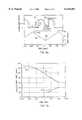
- FIGS. 4a and 4bshow an applied unipolar triangular waveform 60 and the time-dependent position of a single ribbon element 31 for two different time delays, 5 and 120 seconds, after the onset of actuation.
- Graph 62displays the height of the ribbon element 31 versus time 5 seconds after actuation.
- Graph 63displays the height f the ribbon element 31 versus time 120 seconds after actuation.
- the behavior of the ribbon element 31is significantly different 120 seconds 63 after actuation than at 5 seconds 62.
- Measurement of the time intervals t U and t D(shown in FIGS. 4a and 4b) with a time interval analyzer (TIA) provides a convenient means for monitoring the change in response of the ribbon from one actuation to the next.
- TIAtime interval analyzer
- t Uis the time the ribbon element is in contact with the surface (down time) when the voltage of the applied waveform 60 is near its maximum 61U and t D is the time the ribbon element is in contact when the voltage is near its minimum 61D, which is zero in this case.
- FIG. 4bshows the measured TIA data as a function of time delay after initial actuation.
- the ribbon element 31 down time t Uis approximately 130 ⁇ sec and the down time t D is zero because the ribbons do not actuate when the voltage waveform 60 is near zero.
- ribbon chargingbecomes large enough to fully actuate the ribbon when the applied voltage is near zero and t D becomes non-zero 67. If the applied voltage waveform is turned off past this point, the ribbon element 31 will become fully actuated because of the accumulated charge present.
- the ribbonscan be actuated as shown in FIG. 5a with a bipolar triangular waveform 70.
- any dielectric charging that occurs during the positive portion of the waveformis canceled during the negative portion and vice versa, resulting in a stable ribbon response 71.
- the ribbon down timeis equal during both positive and negative portion of the waveform and is independent of time from initial actuation as shown in FIG. 5b.
- the dielectric charging effects that occur with a unipolar ribbon voltage waveform 60prevent proper pulse width modulation of the diffracted light intensity.
- the light intensitycan be modulated with an appropriately chosen DC-free bipolar waveform.
- FIG. 6One scheme is illustrated in FIG. 6 for the case of pulse width modulation.
- the data to be sent to the GLVis provided as a pulse width modulated data stream 50.
- a modulated bipolar voltage 75is applied to the ribbon elements 31.
- the modulated bipolar voltage 75is positive for the first half of the pulse and negative for the second half.
- the ribbon response 77is nearly the same as that of the unipolar waveform in FIG. 3.
- There is a small time interval 79during the change of polarity during which the ribbons are released. With electronics possessing large enough voltage slew, the diffracted light intensity will only be affected for an insignificant interval of time by this brief release.
- each pulse in the waveformcan be divided into several positive and negative polarity portions.
- FIG. 7shows one scheme that is straightforward to implement in a practical circuit.
- the data to be sent to the GLVis provided as a pulse width modulated data stream 50.
- each pulse width in the data stream 50is divided into an equal number positive and negative portions each having the same length ⁇ /2.
- a resulting ribbon response 82is nearly the same as that of the ribbon response in FIG. 6. Because each change of polarity causes the ribbon elements 31 to be released, there can be more than one small time interval 79 within one pulse width.
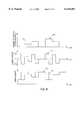
- a clock circuit 84provides a continuous sequence of timing pulses 85 with period ⁇ to an actuation voltage generator 86, which produces a periodic bipolar voltage 87, and to a data generator 88, which produces a pulse width modulated signal 89.
- a modulator 90then uses the pulse width modulated signal 89 as a gate to produce a modulated bipolar voltage 91 which is applied to the ribbon elements 31.
- FIG. 9illustrates the case of pulse amplitude modulation where each pulse interval of a data stream 100 is of a fixed length, and the amplitude is varied from one pulse interval to the next, but has a constant height within each pulse interval.
- the modulated bipolar voltage 110is generated in accordance to the data stream 100 such that each pulse with constant height produces two pulses of equal width and opposite polarity in the modulated bipolar voltage 110.
- the bipolarity of the voltage signalhas to be considered with respect to a bias voltage applied to the bottom conductive layer 22.
- the modulated bipolar voltage 110When the modulated bipolar voltage 110 is applied to the ribbon elements 31, more than two different levels of the ribbon elements is achieved. There is a small time interval 121 during the change of polarity during which the ribbons are released. During this time interval the ribbon element 31 may jump back to the un-actuated state. As before, with electronics possessing large enough voltage slew, the diffracted light intensity will only be affected for an insignificant interval of time by this brief release.
- the bipolar voltage waveforms 75, 80 and 110 in FIGS. 6, 7 and 9contain higher frequencies and larger voltage swings than the unipolar waveforms 52 and 56 in FIG. 3.
- the data generator 88sends the pulse width modulated signal 89 to a modulator 97 and a polarity control counter 95.
- the counter 95keeps track of the total amount of time a certain polarity has been used to actuate the ribbon elements 31. When this time exceeds a specified period, the counter 95 sends a signal to the modulator 97 to switch polarity. The counter 95 is then reset and restarted. The resulting bipolar ribbon voltage 98 is DC-free.
- the bottom conductive layer 22can be biased at a fixed non-zero voltage and a unipolar waveform, whose time average is equal to this bias voltage, can be used to actuate the ribbon elements 31. Electrical isolation of the bottom conductive layer 22 of the electromechanical grating element from the ground plane of the driver circuitry is then preferable. If the bias voltage is time varying, it is possible to minimize charging with a unipolar waveform with only two levels. This scheme requires the time average of the unipolar waveform to be equal to the time average of the bias voltage.
- FIG. 11shows an example of this scheme for the pulse width modulated data stream 50.
- the bias voltage 130is a unipolar square wave with period ⁇ and the ribbon voltage 125 during each interval ⁇ /2 is chosen so as to achieve the desired sate of the ribbon element, either actuated or unactuated. Charging effects are reduced by this scheme as well.
- the unipolar waveformmust contain at least three voltage levels: one voltage greater than the vias voltage, one less than the bias voltage and one equal to the bias voltage. The first two voltage levels produce the actuated state of the ribbon element and the last produces the unactuated state. In practice the time average of the waveform can be slightly different from the bias voltage while still maintaining stable operation of the ribbon elements.
- the above described modulationcan be accomplished with a system as disclosed in the block diagram depicted in FIG. 12.
- the clock circuit(see FIG. 8) provides a continuous sequence of timing pulses 85 to the data generator 88 which produces a pulse width modulated signal 89, and to a bias voltage generator 144 which produces a periodic unipolar bias voltage 145.
- a modulator 148then uses the pulse width modulated signal 89 and the timing pulses 85 from the clock 84 to generate a modulated unipolar voltage 149.
- the desired ribbon responseis achieved by applying the modulated unipolar voltage 149 to the conductive layer 32 of the ribbon elements and applying the periodic unipolar bias voltage 145 to the bottom conductive layer 22.
Landscapes
- Physics & Mathematics (AREA)
- General Physics & Mathematics (AREA)
- Optics & Photonics (AREA)
- Mechanical Light Control Or Optical Switches (AREA)
- Diffracting Gratings Or Hologram Optical Elements (AREA)
- Control Of Indicators Other Than Cathode Ray Tubes (AREA)
Abstract
Description
Claims (14)
Priority Applications (3)
| Application Number | Priority Date | Filing Date | Title |
|---|---|---|---|
| US09/215,106US6144481A (en) | 1998-12-18 | 1998-12-18 | Method and system for actuating electro-mechanical ribbon elements in accordance to a data stream |
| EP99204213AEP1010995A1 (en) | 1998-12-18 | 1999-12-09 | Method and system for actuating electro-mechanical grating elements in accordance to a data stream |
| JP11353571AJP2000180738A (en) | 1998-12-18 | 1999-12-13 | Method of driving electromechanical ribbon member |
Applications Claiming Priority (1)
| Application Number | Priority Date | Filing Date | Title |
|---|---|---|---|
| US09/215,106US6144481A (en) | 1998-12-18 | 1998-12-18 | Method and system for actuating electro-mechanical ribbon elements in accordance to a data stream |
Publications (1)
| Publication Number | Publication Date |
|---|---|
| US6144481Atrue US6144481A (en) | 2000-11-07 |
Family
ID=22801678
Family Applications (1)
| Application Number | Title | Priority Date | Filing Date |
|---|---|---|---|
| US09/215,106Expired - LifetimeUS6144481A (en) | 1998-12-18 | 1998-12-18 | Method and system for actuating electro-mechanical ribbon elements in accordance to a data stream |
Country Status (3)
| Country | Link |
|---|---|
| US (1) | US6144481A (en) |
| EP (1) | EP1010995A1 (en) |
| JP (1) | JP2000180738A (en) |
Cited By (81)
| Publication number | Priority date | Publication date | Assignee | Title |
|---|---|---|---|---|
| US6243194B1 (en)* | 1998-12-18 | 2001-06-05 | Eastman Kodak Company | Electro-mechanical grating device |
| US6282012B1 (en)* | 1999-12-10 | 2001-08-28 | Eastman Kodak Company | Method for damping ribbon elements in a micromechanical grating device by selection of actuation waveform |
| US20020167695A1 (en)* | 2001-03-02 | 2002-11-14 | Senturia Stephen D. | Methods and apparatus for diffractive optical processing using an actuatable structure |
| WO2003021842A3 (en)* | 2001-07-25 | 2003-05-01 | Nantero Inc | Hybrid circuit having nanotube electromechanical memory |
| WO2003060597A3 (en)* | 2001-12-21 | 2003-10-23 | Polychromix Corp | Method and apparatus providing reduced polarization-dependent loss |
| EP1367414A1 (en)* | 2002-05-28 | 2003-12-03 | Sony Corporation | Electrostatic machine element, light diffraction modulation element and image display device |
| US6706402B2 (en) | 2001-07-25 | 2004-03-16 | Nantero, Inc. | Nanotube films and articles |
| US6707591B2 (en) | 2001-04-10 | 2004-03-16 | Silicon Light Machines | Angled illumination for a single order light modulator based projection system |
| US6712480B1 (en) | 2002-09-27 | 2004-03-30 | Silicon Light Machines | Controlled curvature of stressed micro-structures |
| US6714337B1 (en) | 2002-06-28 | 2004-03-30 | Silicon Light Machines | Method and device for modulating a light beam and having an improved gamma response |
| US6724515B1 (en) | 2002-12-31 | 2004-04-20 | Eastman Kodak Company | Conformal grating device for producing enhanced gray levels |
| US6724125B2 (en) | 1999-03-30 | 2004-04-20 | Massachusetts Institute Of Technology | Methods and apparatus for diffractive optical processing using an actuatable structure |
| US6728023B1 (en) | 2002-05-28 | 2004-04-27 | Silicon Light Machines | Optical device arrays with optimized image resolution |
| US6764875B2 (en) | 1998-07-29 | 2004-07-20 | Silicon Light Machines | Method of and apparatus for sealing an hermetic lid to a semiconductor die |
| US6767751B2 (en) | 2002-05-28 | 2004-07-27 | Silicon Light Machines, Inc. | Integrated driver process flow |
| US20040156088A1 (en)* | 2003-02-06 | 2004-08-12 | Evans & Sutherland Computer Corporation | GLV based fiber optic transmitter |
| US6782205B2 (en) | 2001-06-25 | 2004-08-24 | Silicon Light Machines | Method and apparatus for dynamic equalization in wavelength division multiplexing |
| US6784028B2 (en) | 2001-12-28 | 2004-08-31 | Nantero, Inc. | Methods of making electromechanical three-trace junction devices |
| US6800238B1 (en) | 2002-01-15 | 2004-10-05 | Silicon Light Machines, Inc. | Method for domain patterning in low coercive field ferroelectrics |
| US6801354B1 (en) | 2002-08-20 | 2004-10-05 | Silicon Light Machines, Inc. | 2-D diffraction grating for substantially eliminating polarization dependent losses |
| US6806997B1 (en) | 2003-02-28 | 2004-10-19 | Silicon Light Machines, Inc. | Patterned diffractive light modulator ribbon for PDL reduction |
| US6813059B2 (en) | 2002-06-28 | 2004-11-02 | Silicon Light Machines, Inc. | Reduced formation of asperities in contact micro-structures |
| US6822797B1 (en) | 2002-05-31 | 2004-11-23 | Silicon Light Machines, Inc. | Light modulator structure for producing high-contrast operation using zero-order light |
| US6829077B1 (en) | 2003-02-28 | 2004-12-07 | Silicon Light Machines, Inc. | Diffractive light modulator with dynamically rotatable diffraction plane |
| US6829258B1 (en) | 2002-06-26 | 2004-12-07 | Silicon Light Machines, Inc. | Rapidly tunable external cavity laser |
| US6829092B2 (en) | 2001-08-15 | 2004-12-07 | Silicon Light Machines, Inc. | Blazed grating light valve |
| US6835591B2 (en) | 2001-07-25 | 2004-12-28 | Nantero, Inc. | Methods of nanotube films and articles |
| US6844960B2 (en) | 2002-09-24 | 2005-01-18 | Eastman Kodak Company | Microelectromechanical device with continuously variable displacement |
| US6865346B1 (en) | 2001-06-05 | 2005-03-08 | Silicon Light Machines Corporation | Fiber optic transceiver |
| US6872984B1 (en) | 1998-07-29 | 2005-03-29 | Silicon Light Machines Corporation | Method of sealing a hermetic lid to a semiconductor die at an angle |
| US20050099490A1 (en)* | 2003-11-06 | 2005-05-12 | Eastman Kodak Company | High-speed pulse width modulation system and method for linear array spatial light modulators |
| US6908201B2 (en) | 2002-06-28 | 2005-06-21 | Silicon Light Machines Corporation | Micro-support structures |
| US6911682B2 (en) | 2001-12-28 | 2005-06-28 | Nantero, Inc. | Electromechanical three-trace junction devices |
| US6922272B1 (en) | 2003-02-14 | 2005-07-26 | Silicon Light Machines Corporation | Method and apparatus for leveling thermal stress variations in multi-layer MEMS devices |
| US6922273B1 (en) | 2003-02-28 | 2005-07-26 | Silicon Light Machines Corporation | PDL mitigation structure for diffractive MEMS and gratings |
| US6927891B1 (en) | 2002-12-23 | 2005-08-09 | Silicon Light Machines Corporation | Tilt-able grating plane for improved crosstalk in 1×N blaze switches |
| US6928207B1 (en) | 2002-12-12 | 2005-08-09 | Silicon Light Machines Corporation | Apparatus for selectively blocking WDM channels |
| US6934070B1 (en) | 2002-12-18 | 2005-08-23 | Silicon Light Machines Corporation | Chirped optical MEM device |
| US20050191789A1 (en)* | 2000-12-07 | 2005-09-01 | Patel Satyadev R. | Methods for depositing, releasing and packaging micro-electromechanical devices on wafer substrates |
| US6947613B1 (en) | 2003-02-11 | 2005-09-20 | Silicon Light Machines Corporation | Wavelength selective switch and equalizer |
| US20050228285A1 (en)* | 2004-04-01 | 2005-10-13 | Yongli Huang | Capacitive ultrasonic transducers with isolation posts |
| US6956878B1 (en) | 2000-02-07 | 2005-10-18 | Silicon Light Machines Corporation | Method and apparatus for reducing laser speckle using polarization averaging |
| US6956995B1 (en) | 2001-11-09 | 2005-10-18 | Silicon Light Machines Corporation | Optical communication arrangement |
| US6962419B2 (en) | 1998-09-24 | 2005-11-08 | Reflectivity, Inc | Micromirror elements, package for the micromirror elements, and projection system therefor |
| US6987600B1 (en) | 2002-12-17 | 2006-01-17 | Silicon Light Machines Corporation | Arbitrary phase profile for better equalization in dynamic gain equalizer |
| US6991953B1 (en) | 2001-09-13 | 2006-01-31 | Silicon Light Machines Corporation | Microelectronic mechanical system and methods |
| US7006275B2 (en) | 2000-08-30 | 2006-02-28 | Reflectivity, Inc | Packaged micromirror array for a projection display |
| US7023606B2 (en) | 2001-08-03 | 2006-04-04 | Reflectivity, Inc | Micromirror array for projection TV |
| US7027202B1 (en) | 2003-02-28 | 2006-04-11 | Silicon Light Machines Corp | Silicon substrate as a light modulator sacrificial layer |
| US7042611B1 (en) | 2003-03-03 | 2006-05-09 | Silicon Light Machines Corporation | Pre-deflected bias ribbons |
| US7046410B2 (en) | 2001-10-11 | 2006-05-16 | Polychromix, Inc. | Actuatable diffractive optical processor |
| US7054515B1 (en) | 2002-05-30 | 2006-05-30 | Silicon Light Machines Corporation | Diffractive light modulator-based dynamic equalizer with integrated spectral monitor |
| US7057795B2 (en) | 2002-08-20 | 2006-06-06 | Silicon Light Machines Corporation | Micro-structures with individually addressable ribbon pairs |
| US7056758B2 (en) | 2001-07-25 | 2006-06-06 | Nantero, Inc. | Electromechanical memory array using nanotube ribbons and method for making same |
| US7057819B1 (en) | 2002-12-17 | 2006-06-06 | Silicon Light Machines Corporation | High contrast tilting ribbon blazed grating |
| US7068372B1 (en) | 2003-01-28 | 2006-06-27 | Silicon Light Machines Corporation | MEMS interferometer-based reconfigurable optical add-and-drop multiplexor |
| US7075702B2 (en) | 2003-10-30 | 2006-07-11 | Reflectivity, Inc | Micromirror and post arrangements on substrates |
| US7176505B2 (en) | 2001-12-28 | 2007-02-13 | Nantero, Inc. | Electromechanical three-trace junction devices |
| US7177081B2 (en) | 2001-03-08 | 2007-02-13 | Silicon Light Machines Corporation | High contrast grating light valve type device |
| EP1491933A4 (en)* | 2002-04-04 | 2007-06-13 | Sony Corp | Light reflection/diffraction device, light reflection/diffraction device array, and image display |
| US7274078B2 (en) | 2001-07-25 | 2007-09-25 | Nantero, Inc. | Devices having vertically-disposed nanofabric articles and methods of making the same |
| US7286764B1 (en) | 2003-02-03 | 2007-10-23 | Silicon Light Machines Corporation | Reconfigurable modulator-based optical add-and-drop multiplexer |
| US7304357B2 (en) | 2001-07-25 | 2007-12-04 | Nantero, Inc. | Devices having horizontally-disposed nanofabric articles and methods of making the same |
| US7335395B2 (en) | 2002-04-23 | 2008-02-26 | Nantero, Inc. | Methods of using pre-formed nanotubes to make carbon nanotube films, layers, fabrics, ribbons, elements and articles |
| US7391973B1 (en) | 2003-02-28 | 2008-06-24 | Silicon Light Machines Corporation | Two-stage gain equalizer |
| US7560136B2 (en) | 2003-01-13 | 2009-07-14 | Nantero, Inc. | Methods of using thin metal layers to make carbon nanotube films, layers, fabrics, ribbons, elements and articles |
| US7566478B2 (en) | 2001-07-25 | 2009-07-28 | Nantero, Inc. | Methods of making carbon nanotube films, layers, fabrics, ribbons, elements and articles |
| US7791027B2 (en) | 2006-01-31 | 2010-09-07 | Ahura Scientific Inc. | Apparatus and method providing a hand-held spectrometer |
| US20100315595A1 (en)* | 2009-06-15 | 2010-12-16 | Marcus Michael A | Dynamic illumination control for laser projection display |
| US20110025657A1 (en)* | 2009-07-31 | 2011-02-03 | Edward Pakhchyan | Method of operating electromechanical pixels |
| US7891818B2 (en) | 2006-12-12 | 2011-02-22 | Evans & Sutherland Computer Corporation | System and method for aligning RGB light in a single modulator projector |
| US20110134344A1 (en)* | 2009-12-08 | 2011-06-09 | Marcus Michael A | Dynamic illumination control for laser projection display |
| US8077378B1 (en) | 2008-11-12 | 2011-12-13 | Evans & Sutherland Computer Corporation | Calibration system and method for light modulation device |
| US8358317B2 (en) | 2008-05-23 | 2013-01-22 | Evans & Sutherland Computer Corporation | System and method for displaying a planar image on a curved surface |
| US8702248B1 (en) | 2008-06-11 | 2014-04-22 | Evans & Sutherland Computer Corporation | Projection method for reducing interpixel gaps on a viewing surface |
| US20140168750A1 (en)* | 2012-09-24 | 2014-06-19 | Alces Technology, Inc. | Digital drive signals for analog MEMS ribbon arrays |
| US9641826B1 (en) | 2011-10-06 | 2017-05-02 | Evans & Sutherland Computer Corporation | System and method for displaying distant 3-D stereo on a dome surface |
| US10746983B2 (en) | 2017-08-29 | 2020-08-18 | Silicon Light Machines Corporation | Spatial light modulators for phased-array applications |
| US11016287B2 (en) | 2018-11-08 | 2021-05-25 | Silicon Light Machines Corporation | High étendue spatial light modulator |
| US12117606B2 (en) | 2019-08-27 | 2024-10-15 | SCREEN Holdings Co., Ltd. | MEMs phased-array for LiDAR applications |
| US12436242B2 (en) | 2021-02-12 | 2025-10-07 | Silicon Light Machines Corporation | High contrast MEMS phased-array |
Families Citing this family (11)
| Publication number | Priority date | Publication date | Assignee | Title |
|---|---|---|---|---|
| JP4487460B2 (en)* | 2001-09-05 | 2010-06-23 | ソニー株式会社 | Thin film optical device |
| JP3558066B2 (en) | 2002-02-19 | 2004-08-25 | ソニー株式会社 | MEMS element and its manufacturing method, light modulation element, GLV device and its manufacturing method, and laser display |
| JP3690598B2 (en) | 2002-03-19 | 2005-08-31 | 大日本スクリーン製造株式会社 | Image recording device |
| JP2004061937A (en)* | 2002-07-30 | 2004-02-26 | Japan Aviation Electronics Industry Ltd | Micro movable device |
| US6717714B1 (en)* | 2002-12-16 | 2004-04-06 | Eastman Kodak Company | Method and system for generating enhanced gray levels in an electromechanical grating display |
| US7348111B2 (en)* | 2003-05-14 | 2008-03-25 | Agfa Corporation | Reduction of imaging artifacts in a platesetter having a diffractive modulator |
| US6856449B2 (en)* | 2003-07-10 | 2005-02-15 | Evans & Sutherland Computer Corporation | Ultra-high resolution light modulation control system and method |
| US7072090B2 (en)* | 2004-04-22 | 2006-07-04 | Micronic Laser Systems Ab | Addressing of an SLM |
| JP5160935B2 (en)* | 2008-03-31 | 2013-03-13 | 日本電信電話株式会社 | Mirror device and mirror array |
| JP6805891B2 (en)* | 2017-03-01 | 2020-12-23 | 株式会社リコー | Spectral measuring instruments, spectroscopic devices and spectroscopic systems |
| JP7394319B2 (en)* | 2017-05-11 | 2023-12-08 | ネオリティクス,インコーポレイテッド | Adaptive optics analyzer with automatic drift control and high dynamic range |
Citations (12)
| Publication number | Priority date | Publication date | Assignee | Title |
|---|---|---|---|---|
| US4011009A (en)* | 1975-05-27 | 1977-03-08 | Xerox Corporation | Reflection diffraction grating having a controllable blaze angle |
| US4360900A (en)* | 1978-11-27 | 1982-11-23 | Texas Instruments Incorporated | Non-volatile semiconductor memory elements |
| US4492435A (en)* | 1982-07-02 | 1985-01-08 | Xerox Corporation | Multiple array full width electro mechanical modulator |
| US4596992A (en)* | 1984-08-31 | 1986-06-24 | Texas Instruments Incorporated | Linear spatial light modulator and printer |
| US5115344A (en)* | 1990-10-03 | 1992-05-19 | Motorola, Inc. | Tunable diffraction grating |
| US5311360A (en)* | 1992-04-28 | 1994-05-10 | The Board Of Trustees Of The Leland Stanford, Junior University | Method and apparatus for modulating a light beam |
| US5661593A (en)* | 1992-10-01 | 1997-08-26 | Engle; Craig D. | Linear electrostatic modulator |
| US5757536A (en)* | 1995-08-30 | 1998-05-26 | Sandia Corporation | Electrically-programmable diffraction grating |
| US5808797A (en)* | 1992-04-28 | 1998-09-15 | Silicon Light Machines | Method and apparatus for modulating a light beam |
| US5841579A (en)* | 1995-06-07 | 1998-11-24 | Silicon Light Machines | Flat diffraction grating light valve |
| US5844711A (en)* | 1997-01-10 | 1998-12-01 | Northrop Grumman Corporation | Tunable spatial light modulator |
| US5949570A (en)* | 1995-06-20 | 1999-09-07 | Matsushita Electric Industrial Co., Ltd. | Diffractive optical modulator and method for producing the same, infrared sensor including such a diffractive optical modulator and method for producing the same, and display device including such a diffractive optical modulator |
Family Cites Families (3)
| Publication number | Priority date | Publication date | Assignee | Title |
|---|---|---|---|---|
| EP0614101A3 (en)* | 1993-02-03 | 1994-10-19 | Canon Kk | Optical deflector and method of manufacturing the same. |
| JP3290332B2 (en)* | 1994-06-21 | 2002-06-10 | 松下電器産業株式会社 | Emission efficiency control element and method of manufacturing the same, and infrared sensor provided with the emission efficiency control element and method of manufacturing the same |
| US5920418A (en)* | 1994-06-21 | 1999-07-06 | Matsushita Electric Industrial Co., Ltd. | Diffractive optical modulator and method for producing the same, infrared sensor including such a diffractive optical modulator and method for producing the same, and display device including such a diffractive optical modulator |
- 1998
- 1998-12-18USUS09/215,106patent/US6144481A/ennot_activeExpired - Lifetime
- 1999
- 1999-12-09EPEP99204213Apatent/EP1010995A1/ennot_activeWithdrawn
- 1999-12-13JPJP11353571Apatent/JP2000180738A/enactivePending
Patent Citations (14)
| Publication number | Priority date | Publication date | Assignee | Title |
|---|---|---|---|---|
| US4011009A (en)* | 1975-05-27 | 1977-03-08 | Xerox Corporation | Reflection diffraction grating having a controllable blaze angle |
| US4360900A (en)* | 1978-11-27 | 1982-11-23 | Texas Instruments Incorporated | Non-volatile semiconductor memory elements |
| US4492435A (en)* | 1982-07-02 | 1985-01-08 | Xerox Corporation | Multiple array full width electro mechanical modulator |
| US4596992A (en)* | 1984-08-31 | 1986-06-24 | Texas Instruments Incorporated | Linear spatial light modulator and printer |
| US5115344A (en)* | 1990-10-03 | 1992-05-19 | Motorola, Inc. | Tunable diffraction grating |
| US5459610A (en)* | 1992-04-28 | 1995-10-17 | The Board Of Trustees Of The Leland Stanford, Junior University | Deformable grating apparatus for modulating a light beam and including means for obviating stiction between grating elements and underlying substrate |
| US5311360A (en)* | 1992-04-28 | 1994-05-10 | The Board Of Trustees Of The Leland Stanford, Junior University | Method and apparatus for modulating a light beam |
| US5677783A (en)* | 1992-04-28 | 1997-10-14 | The Board Of Trustees Of The Leland Stanford, Junior University | Method of making a deformable grating apparatus for modulating a light beam and including means for obviating stiction between grating elements and underlying substrate |
| US5808797A (en)* | 1992-04-28 | 1998-09-15 | Silicon Light Machines | Method and apparatus for modulating a light beam |
| US5661593A (en)* | 1992-10-01 | 1997-08-26 | Engle; Craig D. | Linear electrostatic modulator |
| US5841579A (en)* | 1995-06-07 | 1998-11-24 | Silicon Light Machines | Flat diffraction grating light valve |
| US5949570A (en)* | 1995-06-20 | 1999-09-07 | Matsushita Electric Industrial Co., Ltd. | Diffractive optical modulator and method for producing the same, infrared sensor including such a diffractive optical modulator and method for producing the same, and display device including such a diffractive optical modulator |
| US5757536A (en)* | 1995-08-30 | 1998-05-26 | Sandia Corporation | Electrically-programmable diffraction grating |
| US5844711A (en)* | 1997-01-10 | 1998-12-01 | Northrop Grumman Corporation | Tunable spatial light modulator |
Non-Patent Citations (2)
| Title |
|---|
| C. Cabuz et al., High Reliability Touch Mode Electrostatic Actuators (TMEA), Solid State Sensor and Actuator Workshop , Hilton Head Island, South Carolina, Jun. 8 11, 1998, pp. 296 299.* |
| C. Cabuz et al., High Reliability Touch-Mode Electrostatic Actuators (TMEA), Solid-State Sensor and Actuator Workshop, Hilton Head Island, South Carolina, Jun. 8-11, 1998, pp. 296-299. |
Cited By (120)
| Publication number | Priority date | Publication date | Assignee | Title |
|---|---|---|---|---|
| US6764875B2 (en) | 1998-07-29 | 2004-07-20 | Silicon Light Machines | Method of and apparatus for sealing an hermetic lid to a semiconductor die |
| US6872984B1 (en) | 1998-07-29 | 2005-03-29 | Silicon Light Machines Corporation | Method of sealing a hermetic lid to a semiconductor die at an angle |
| US6962419B2 (en) | 1998-09-24 | 2005-11-08 | Reflectivity, Inc | Micromirror elements, package for the micromirror elements, and projection system therefor |
| US6243194B1 (en)* | 1998-12-18 | 2001-06-05 | Eastman Kodak Company | Electro-mechanical grating device |
| US6724125B2 (en) | 1999-03-30 | 2004-04-20 | Massachusetts Institute Of Technology | Methods and apparatus for diffractive optical processing using an actuatable structure |
| US6282012B1 (en)* | 1999-12-10 | 2001-08-28 | Eastman Kodak Company | Method for damping ribbon elements in a micromechanical grating device by selection of actuation waveform |
| US6956878B1 (en) | 2000-02-07 | 2005-10-18 | Silicon Light Machines Corporation | Method and apparatus for reducing laser speckle using polarization averaging |
| US7172296B2 (en) | 2000-08-30 | 2007-02-06 | Reflectivity, Inc | Projection display |
| US7167297B2 (en) | 2000-08-30 | 2007-01-23 | Reflectivity, Inc | Micromirror array |
| US7300162B2 (en) | 2000-08-30 | 2007-11-27 | Texas Instruments Incorporated | Projection display |
| US7012731B2 (en) | 2000-08-30 | 2006-03-14 | Reflectivity, Inc | Packaged micromirror array for a projection display |
| US7018052B2 (en) | 2000-08-30 | 2006-03-28 | Reflectivity, Inc | Projection TV with improved micromirror array |
| US7006275B2 (en) | 2000-08-30 | 2006-02-28 | Reflectivity, Inc | Packaged micromirror array for a projection display |
| US7262817B2 (en) | 2000-08-30 | 2007-08-28 | Texas Instruments Incorporated | Rear projection TV with improved micromirror array |
| US7196740B2 (en) | 2000-08-30 | 2007-03-27 | Texas Instruments Incorporated | Projection TV with improved micromirror array |
| US7655492B2 (en) | 2000-12-07 | 2010-02-02 | Texas Instruments Incorporated | Methods for depositing, releasing and packaging micro-electromechanical devices on wafer substrates |
| US7573111B2 (en) | 2000-12-07 | 2009-08-11 | Texas Instruments Incorporated | Methods for depositing, releasing and packaging micro-electromechanical devices on wafer substrates |
| US7286278B2 (en) | 2000-12-07 | 2007-10-23 | Texas Instruments Incorporated | Methods for depositing, releasing and packaging micro-electromechanical devices on wafer substrates |
| US20050191789A1 (en)* | 2000-12-07 | 2005-09-01 | Patel Satyadev R. | Methods for depositing, releasing and packaging micro-electromechanical devices on wafer substrates |
| US7671428B2 (en) | 2000-12-07 | 2010-03-02 | Texas Instruments Incorporated | Methods for depositing, releasing and packaging micro-electromechanical devices on wafer substrates |
| US20020167695A1 (en)* | 2001-03-02 | 2002-11-14 | Senturia Stephen D. | Methods and apparatus for diffractive optical processing using an actuatable structure |
| US7177081B2 (en) | 2001-03-08 | 2007-02-13 | Silicon Light Machines Corporation | High contrast grating light valve type device |
| US6707591B2 (en) | 2001-04-10 | 2004-03-16 | Silicon Light Machines | Angled illumination for a single order light modulator based projection system |
| US6865346B1 (en) | 2001-06-05 | 2005-03-08 | Silicon Light Machines Corporation | Fiber optic transceiver |
| US6782205B2 (en) | 2001-06-25 | 2004-08-24 | Silicon Light Machines | Method and apparatus for dynamic equalization in wavelength division multiplexing |
| US7274078B2 (en) | 2001-07-25 | 2007-09-25 | Nantero, Inc. | Devices having vertically-disposed nanofabric articles and methods of making the same |
| US7304357B2 (en) | 2001-07-25 | 2007-12-04 | Nantero, Inc. | Devices having horizontally-disposed nanofabric articles and methods of making the same |
| US7056758B2 (en) | 2001-07-25 | 2006-06-06 | Nantero, Inc. | Electromechanical memory array using nanotube ribbons and method for making same |
| US7745810B2 (en) | 2001-07-25 | 2010-06-29 | Nantero, Inc. | Nanotube films and articles |
| US6835591B2 (en) | 2001-07-25 | 2004-12-28 | Nantero, Inc. | Methods of nanotube films and articles |
| US7264990B2 (en) | 2001-07-25 | 2007-09-04 | Nantero, Inc. | Methods of nanotubes films and articles |
| US7298016B2 (en) | 2001-07-25 | 2007-11-20 | Nantero, Inc. | Electromechanical memory array using nanotube ribbons and method for making same |
| WO2003021842A3 (en)* | 2001-07-25 | 2003-05-01 | Nantero Inc | Hybrid circuit having nanotube electromechanical memory |
| US7335528B2 (en) | 2001-07-25 | 2008-02-26 | Nantero, Inc. | Methods of nanotube films and articles |
| US6942921B2 (en) | 2001-07-25 | 2005-09-13 | Nantero, Inc. | Nanotube films and articles |
| US7342818B2 (en) | 2001-07-25 | 2008-03-11 | Nantero, Inc. | Hybrid circuit having nanotube electromechanical memory |
| US7566478B2 (en) | 2001-07-25 | 2009-07-28 | Nantero, Inc. | Methods of making carbon nanotube films, layers, fabrics, ribbons, elements and articles |
| US6706402B2 (en) | 2001-07-25 | 2004-03-16 | Nantero, Inc. | Nanotube films and articles |
| US7023606B2 (en) | 2001-08-03 | 2006-04-04 | Reflectivity, Inc | Micromirror array for projection TV |
| US6829092B2 (en) | 2001-08-15 | 2004-12-07 | Silicon Light Machines, Inc. | Blazed grating light valve |
| US7049164B2 (en) | 2001-09-13 | 2006-05-23 | Silicon Light Machines Corporation | Microelectronic mechanical system and methods |
| US6991953B1 (en) | 2001-09-13 | 2006-01-31 | Silicon Light Machines Corporation | Microelectronic mechanical system and methods |
| US7046410B2 (en) | 2001-10-11 | 2006-05-16 | Polychromix, Inc. | Actuatable diffractive optical processor |
| US6956995B1 (en) | 2001-11-09 | 2005-10-18 | Silicon Light Machines Corporation | Optical communication arrangement |
| US6768589B2 (en) | 2001-12-21 | 2004-07-27 | Polychromix Corporation | Method and apparatus providing reduced polarization-dependent loss |
| US20040027667A1 (en)* | 2001-12-21 | 2004-02-12 | Deutsch Erik R. | Method and apparatus providing reduced polarization-dependent loss |
| WO2003060597A3 (en)* | 2001-12-21 | 2003-10-23 | Polychromix Corp | Method and apparatus providing reduced polarization-dependent loss |
| US6911682B2 (en) | 2001-12-28 | 2005-06-28 | Nantero, Inc. | Electromechanical three-trace junction devices |
| US6784028B2 (en) | 2001-12-28 | 2004-08-31 | Nantero, Inc. | Methods of making electromechanical three-trace junction devices |
| US7521736B2 (en) | 2001-12-28 | 2009-04-21 | Nantero, Inc. | Electromechanical three-trace junction devices |
| US6979590B2 (en) | 2001-12-28 | 2005-12-27 | Nantero, Inc. | Methods of making electromechanical three-trace junction devices |
| US7915066B2 (en) | 2001-12-28 | 2011-03-29 | Nantero, Inc. | Methods of making electromechanical three-trace junction devices |
| US7176505B2 (en) | 2001-12-28 | 2007-02-13 | Nantero, Inc. | Electromechanical three-trace junction devices |
| US6800238B1 (en) | 2002-01-15 | 2004-10-05 | Silicon Light Machines, Inc. | Method for domain patterning in low coercive field ferroelectrics |
| EP1491933A4 (en)* | 2002-04-04 | 2007-06-13 | Sony Corp | Light reflection/diffraction device, light reflection/diffraction device array, and image display |
| US7335395B2 (en) | 2002-04-23 | 2008-02-26 | Nantero, Inc. | Methods of using pre-formed nanotubes to make carbon nanotube films, layers, fabrics, ribbons, elements and articles |
| US6767751B2 (en) | 2002-05-28 | 2004-07-27 | Silicon Light Machines, Inc. | Integrated driver process flow |
| US6728023B1 (en) | 2002-05-28 | 2004-04-27 | Silicon Light Machines | Optical device arrays with optimized image resolution |
| US6813061B2 (en) | 2002-05-28 | 2004-11-02 | Sony Corporation | Electrostatic machine element, light diffraction modulation element and image display device |
| EP1367414A1 (en)* | 2002-05-28 | 2003-12-03 | Sony Corporation | Electrostatic machine element, light diffraction modulation element and image display device |
| US7054515B1 (en) | 2002-05-30 | 2006-05-30 | Silicon Light Machines Corporation | Diffractive light modulator-based dynamic equalizer with integrated spectral monitor |
| US6822797B1 (en) | 2002-05-31 | 2004-11-23 | Silicon Light Machines, Inc. | Light modulator structure for producing high-contrast operation using zero-order light |
| US6829258B1 (en) | 2002-06-26 | 2004-12-07 | Silicon Light Machines, Inc. | Rapidly tunable external cavity laser |
| US6714337B1 (en) | 2002-06-28 | 2004-03-30 | Silicon Light Machines | Method and device for modulating a light beam and having an improved gamma response |
| US6813059B2 (en) | 2002-06-28 | 2004-11-02 | Silicon Light Machines, Inc. | Reduced formation of asperities in contact micro-structures |
| US6908201B2 (en) | 2002-06-28 | 2005-06-21 | Silicon Light Machines Corporation | Micro-support structures |
| US7057795B2 (en) | 2002-08-20 | 2006-06-06 | Silicon Light Machines Corporation | Micro-structures with individually addressable ribbon pairs |
| US6801354B1 (en) | 2002-08-20 | 2004-10-05 | Silicon Light Machines, Inc. | 2-D diffraction grating for substantially eliminating polarization dependent losses |
| US6844960B2 (en) | 2002-09-24 | 2005-01-18 | Eastman Kodak Company | Microelectromechanical device with continuously variable displacement |
| US6919983B2 (en) | 2002-09-24 | 2005-07-19 | Eastman Kodak Company | Microelectromechanical device with continuously variable displacement |
| US20050094243A1 (en)* | 2002-09-24 | 2005-05-05 | Eastman Kodak Company | Microelectromechanical device with continuously variable displacement |
| US6712480B1 (en) | 2002-09-27 | 2004-03-30 | Silicon Light Machines | Controlled curvature of stressed micro-structures |
| US6928207B1 (en) | 2002-12-12 | 2005-08-09 | Silicon Light Machines Corporation | Apparatus for selectively blocking WDM channels |
| US6987600B1 (en) | 2002-12-17 | 2006-01-17 | Silicon Light Machines Corporation | Arbitrary phase profile for better equalization in dynamic gain equalizer |
| US7057819B1 (en) | 2002-12-17 | 2006-06-06 | Silicon Light Machines Corporation | High contrast tilting ribbon blazed grating |
| US6934070B1 (en) | 2002-12-18 | 2005-08-23 | Silicon Light Machines Corporation | Chirped optical MEM device |
| US6927891B1 (en) | 2002-12-23 | 2005-08-09 | Silicon Light Machines Corporation | Tilt-able grating plane for improved crosstalk in 1×N blaze switches |
| US6724515B1 (en) | 2002-12-31 | 2004-04-20 | Eastman Kodak Company | Conformal grating device for producing enhanced gray levels |
| CN100397140C (en)* | 2002-12-31 | 2008-06-25 | 伊斯曼柯达公司 | Proper shaped grid device for producing intensified grey level |
| US7560136B2 (en) | 2003-01-13 | 2009-07-14 | Nantero, Inc. | Methods of using thin metal layers to make carbon nanotube films, layers, fabrics, ribbons, elements and articles |
| US7068372B1 (en) | 2003-01-28 | 2006-06-27 | Silicon Light Machines Corporation | MEMS interferometer-based reconfigurable optical add-and-drop multiplexor |
| US7286764B1 (en) | 2003-02-03 | 2007-10-23 | Silicon Light Machines Corporation | Reconfigurable modulator-based optical add-and-drop multiplexer |
| US20040156088A1 (en)* | 2003-02-06 | 2004-08-12 | Evans & Sutherland Computer Corporation | GLV based fiber optic transmitter |
| US7113320B2 (en) | 2003-02-06 | 2006-09-26 | Evans & Sutherland Computer Corporation | GLV based fiber optic transmitter |
| US6947613B1 (en) | 2003-02-11 | 2005-09-20 | Silicon Light Machines Corporation | Wavelength selective switch and equalizer |
| US6922272B1 (en) | 2003-02-14 | 2005-07-26 | Silicon Light Machines Corporation | Method and apparatus for leveling thermal stress variations in multi-layer MEMS devices |
| US7027202B1 (en) | 2003-02-28 | 2006-04-11 | Silicon Light Machines Corp | Silicon substrate as a light modulator sacrificial layer |
| US6922273B1 (en) | 2003-02-28 | 2005-07-26 | Silicon Light Machines Corporation | PDL mitigation structure for diffractive MEMS and gratings |
| US6806997B1 (en) | 2003-02-28 | 2004-10-19 | Silicon Light Machines, Inc. | Patterned diffractive light modulator ribbon for PDL reduction |
| US6829077B1 (en) | 2003-02-28 | 2004-12-07 | Silicon Light Machines, Inc. | Diffractive light modulator with dynamically rotatable diffraction plane |
| US7391973B1 (en) | 2003-02-28 | 2008-06-24 | Silicon Light Machines Corporation | Two-stage gain equalizer |
| US7042611B1 (en) | 2003-03-03 | 2006-05-09 | Silicon Light Machines Corporation | Pre-deflected bias ribbons |
| US7362493B2 (en) | 2003-10-30 | 2008-04-22 | Texas Instruments Incorporated | Micromirror and post arrangements on substrates |
| US7075702B2 (en) | 2003-10-30 | 2006-07-11 | Reflectivity, Inc | Micromirror and post arrangements on substrates |
| US7148910B2 (en) | 2003-11-06 | 2006-12-12 | Eastman Kodak Company | High-speed pulse width modulation system and method for linear array spatial light modulators |
| US20050099490A1 (en)* | 2003-11-06 | 2005-05-12 | Eastman Kodak Company | High-speed pulse width modulation system and method for linear array spatial light modulators |
| US20050228285A1 (en)* | 2004-04-01 | 2005-10-13 | Yongli Huang | Capacitive ultrasonic transducers with isolation posts |
| US7530952B2 (en) | 2004-04-01 | 2009-05-12 | The Board Of Trustees Of The Leland Stanford Junior University | Capacitive ultrasonic transducers with isolation posts |
| US7791027B2 (en) | 2006-01-31 | 2010-09-07 | Ahura Scientific Inc. | Apparatus and method providing a hand-held spectrometer |
| US7891818B2 (en) | 2006-12-12 | 2011-02-22 | Evans & Sutherland Computer Corporation | System and method for aligning RGB light in a single modulator projector |
| US8358317B2 (en) | 2008-05-23 | 2013-01-22 | Evans & Sutherland Computer Corporation | System and method for displaying a planar image on a curved surface |
| US8702248B1 (en) | 2008-06-11 | 2014-04-22 | Evans & Sutherland Computer Corporation | Projection method for reducing interpixel gaps on a viewing surface |
| US8077378B1 (en) | 2008-11-12 | 2011-12-13 | Evans & Sutherland Computer Corporation | Calibration system and method for light modulation device |
| US8864313B2 (en) | 2009-06-15 | 2014-10-21 | Eastman Kodak Company | Dynamic illumination control for laser projection display |
| WO2010147627A1 (en) | 2009-06-15 | 2010-12-23 | Eastman Kodak Company | Dynamic illumination control for laser projection display |
| US20100315595A1 (en)* | 2009-06-15 | 2010-12-16 | Marcus Michael A | Dynamic illumination control for laser projection display |
| US20110025657A1 (en)* | 2009-07-31 | 2011-02-03 | Edward Pakhchyan | Method of operating electromechanical pixels |
| US8416224B2 (en)* | 2009-07-31 | 2013-04-09 | Edward Pakhchyan | Method of operating an array of electromechanical pixels resulting in efficient and reliable operation of light modulating elements |
| US8330870B2 (en) | 2009-12-08 | 2012-12-11 | Eastman Kodak Company | Dynamic illumination control for laser projection display |
| US8730399B2 (en) | 2009-12-08 | 2014-05-20 | Eastman Kodak Company | Dynamic illumination control for laser projection display |
| US20110134344A1 (en)* | 2009-12-08 | 2011-06-09 | Marcus Michael A | Dynamic illumination control for laser projection display |
| US9641826B1 (en) | 2011-10-06 | 2017-05-02 | Evans & Sutherland Computer Corporation | System and method for displaying distant 3-D stereo on a dome surface |
| US10110876B1 (en) | 2011-10-06 | 2018-10-23 | Evans & Sutherland Computer Corporation | System and method for displaying images in 3-D stereo |
| US9036243B2 (en)* | 2012-09-24 | 2015-05-19 | Alces Technology, Inc. | Digital drive signals for analog MEMS ribbon arrays |
| US20140168750A1 (en)* | 2012-09-24 | 2014-06-19 | Alces Technology, Inc. | Digital drive signals for analog MEMS ribbon arrays |
| US10746983B2 (en) | 2017-08-29 | 2020-08-18 | Silicon Light Machines Corporation | Spatial light modulators for phased-array applications |
| US11662571B2 (en) | 2017-08-29 | 2023-05-30 | Silicon Light Machines Corporation | Spatial light modulators for phased-array applications |
| US11016287B2 (en) | 2018-11-08 | 2021-05-25 | Silicon Light Machines Corporation | High étendue spatial light modulator |
| US12117606B2 (en) | 2019-08-27 | 2024-10-15 | SCREEN Holdings Co., Ltd. | MEMs phased-array for LiDAR applications |
| US12436242B2 (en) | 2021-02-12 | 2025-10-07 | Silicon Light Machines Corporation | High contrast MEMS phased-array |
Also Published As
| Publication number | Publication date |
|---|---|
| EP1010995A1 (en) | 2000-06-21 |
| JP2000180738A (en) | 2000-06-30 |
Similar Documents
| Publication | Publication Date | Title |
|---|---|---|
| US6144481A (en) | Method and system for actuating electro-mechanical ribbon elements in accordance to a data stream | |
| US6038057A (en) | Method and system for actuating electro-mechanical ribbon elements in accordance to a data stream | |
| US11662571B2 (en) | Spatial light modulators for phased-array applications | |
| US5221989A (en) | Longitudinal plzt spatial light modulator | |
| US6335831B2 (en) | Multilevel mechanical grating device | |
| US5844711A (en) | Tunable spatial light modulator | |
| US5677783A (en) | Method of making a deformable grating apparatus for modulating a light beam and including means for obviating stiction between grating elements and underlying substrate | |
| US5455709A (en) | Total internal reflection spatial light modulation apparatus and method of fabrication thereof | |
| Hornbeck et al. | Bistable deformable mirror device | |
| RU2166784C2 (en) | Matrix of thin-film controlled mirrors for usage in optical projection system | |
| US20020122239A1 (en) | Reflective spatial light modulator with deflectable elements formed on a light transmissive substrate | |
| US6844960B2 (en) | Microelectromechanical device with continuously variable displacement | |
| WO2007091053A1 (en) | Optical modulator | |
| US6259550B1 (en) | Phase-modulating microstructures for highly integrated surface light modulators | |
| EP0352302B1 (en) | Phase controlled light deflector | |
| US20050117223A1 (en) | Diffractive wave modulating devices | |
| US6243194B1 (en) | Electro-mechanical grating device | |
| US8064123B2 (en) | Mirror device and MEMS device comprising layered electrode | |
| EP0706702B1 (en) | Spatial light modulator | |
| US7215461B1 (en) | MEMS devices with increased damping for suspended movable structures | |
| EP1296171A2 (en) | Electro-mechanical grating device having a continuously controllable diffraction efficiency | |
| US20100067096A1 (en) | Structure body electrically connected via semiconductor material layer | |
| KR100781367B1 (en) | Spatial optical modulator having a protective layer on a light reflective layer | |
| Bernstein et al. | MEMS tilt-mirror spatial light modulator for a dynamic spectral equalizer | |
| KR20030091803A (en) | Electrostatic machine element, light diffraction modulation element and image display device |
Legal Events
| Date | Code | Title | Description |
|---|---|---|---|
| AS | Assignment | Owner name:EASTMAN KODAK COMPANY, NEW YORK Free format text:ASSIGNMENT OF ASSIGNORS INTEREST;ASSIGNORS:KOWARZ, MAREK W.;KARNS, DARREN;KRUSCHWITZ, BRIAN E.;AND OTHERS;REEL/FRAME:009796/0551;SIGNING DATES FROM 19981216 TO 19990223 | |
| STCF | Information on status: patent grant | Free format text:PATENTED CASE | |
| FEPP | Fee payment procedure | Free format text:PAYOR NUMBER ASSIGNED (ORIGINAL EVENT CODE: ASPN); ENTITY STATUS OF PATENT OWNER: LARGE ENTITY | |
| FPAY | Fee payment | Year of fee payment:4 | |
| FPAY | Fee payment | Year of fee payment:8 | |
| AS | Assignment | Owner name:CITICORP NORTH AMERICA, INC., AS AGENT, NEW YORK Free format text:SECURITY INTEREST;ASSIGNORS:EASTMAN KODAK COMPANY;PAKON, INC.;REEL/FRAME:028201/0420 Effective date:20120215 | |
| FPAY | Fee payment | Year of fee payment:12 | |
| AS | Assignment | Owner name:WILMINGTON TRUST, NATIONAL ASSOCIATION, AS AGENT, MINNESOTA Free format text:PATENT SECURITY AGREEMENT;ASSIGNORS:EASTMAN KODAK COMPANY;PAKON, INC.;REEL/FRAME:030122/0235 Effective date:20130322 Owner name:WILMINGTON TRUST, NATIONAL ASSOCIATION, AS AGENT, Free format text:PATENT SECURITY AGREEMENT;ASSIGNORS:EASTMAN KODAK COMPANY;PAKON, INC.;REEL/FRAME:030122/0235 Effective date:20130322 | |
| AS | Assignment | Owner name:BANK OF AMERICA N.A., AS AGENT, MASSACHUSETTS Free format text:INTELLECTUAL PROPERTY SECURITY AGREEMENT (ABL);ASSIGNORS:EASTMAN KODAK COMPANY;FAR EAST DEVELOPMENT LTD.;FPC INC.;AND OTHERS;REEL/FRAME:031162/0117 Effective date:20130903 Owner name:JPMORGAN CHASE BANK, N.A., AS ADMINISTRATIVE, DELAWARE Free format text:INTELLECTUAL PROPERTY SECURITY AGREEMENT (FIRST LIEN);ASSIGNORS:EASTMAN KODAK COMPANY;FAR EAST DEVELOPMENT LTD.;FPC INC.;AND OTHERS;REEL/FRAME:031158/0001 Effective date:20130903 Owner name:BARCLAYS BANK PLC, AS ADMINISTRATIVE AGENT, NEW YORK Free format text:INTELLECTUAL PROPERTY SECURITY AGREEMENT (SECOND LIEN);ASSIGNORS:EASTMAN KODAK COMPANY;FAR EAST DEVELOPMENT LTD.;FPC INC.;AND OTHERS;REEL/FRAME:031159/0001 Effective date:20130903 Owner name:JPMORGAN CHASE BANK, N.A., AS ADMINISTRATIVE, DELA Free format text:INTELLECTUAL PROPERTY SECURITY AGREEMENT (FIRST LIEN);ASSIGNORS:EASTMAN KODAK COMPANY;FAR EAST DEVELOPMENT LTD.;FPC INC.;AND OTHERS;REEL/FRAME:031158/0001 Effective date:20130903 Owner name:PAKON, INC., NEW YORK Free format text:RELEASE OF SECURITY INTEREST IN PATENTS;ASSIGNORS:CITICORP NORTH AMERICA, INC., AS SENIOR DIP AGENT;WILMINGTON TRUST, NATIONAL ASSOCIATION, AS JUNIOR DIP AGENT;REEL/FRAME:031157/0451 Effective date:20130903 Owner name:BARCLAYS BANK PLC, AS ADMINISTRATIVE AGENT, NEW YO Free format text:INTELLECTUAL PROPERTY SECURITY AGREEMENT (SECOND LIEN);ASSIGNORS:EASTMAN KODAK COMPANY;FAR EAST DEVELOPMENT LTD.;FPC INC.;AND OTHERS;REEL/FRAME:031159/0001 Effective date:20130903 Owner name:EASTMAN KODAK COMPANY, NEW YORK Free format text:RELEASE OF SECURITY INTEREST IN PATENTS;ASSIGNORS:CITICORP NORTH AMERICA, INC., AS SENIOR DIP AGENT;WILMINGTON TRUST, NATIONAL ASSOCIATION, AS JUNIOR DIP AGENT;REEL/FRAME:031157/0451 Effective date:20130903 | |
| AS | Assignment | Owner name:CREO MANUFACTURING AMERICA LLC, NEW YORK Free format text:RELEASE BY SECURED PARTY;ASSIGNOR:JP MORGAN CHASE BANK, N.A., AS ADMINISTRATIVE AGENT;REEL/FRAME:049814/0001 Effective date:20190617 Owner name:KODAK AVIATION LEASING LLC, NEW YORK Free format text:RELEASE BY SECURED PARTY;ASSIGNOR:JP MORGAN CHASE BANK, N.A., AS ADMINISTRATIVE AGENT;REEL/FRAME:049814/0001 Effective date:20190617 Owner name:KODAK REALTY, INC., NEW YORK Free format text:RELEASE BY SECURED PARTY;ASSIGNOR:JP MORGAN CHASE BANK, N.A., AS ADMINISTRATIVE AGENT;REEL/FRAME:049814/0001 Effective date:20190617 Owner name:KODAK PHILIPPINES, LTD., NEW YORK Free format text:RELEASE BY SECURED PARTY;ASSIGNOR:JP MORGAN CHASE BANK, N.A., AS ADMINISTRATIVE AGENT;REEL/FRAME:049814/0001 Effective date:20190617 Owner name:KODAK (NEAR EAST), INC., NEW YORK Free format text:RELEASE BY SECURED PARTY;ASSIGNOR:JP MORGAN CHASE BANK, N.A., AS ADMINISTRATIVE AGENT;REEL/FRAME:049814/0001 Effective date:20190617 Owner name:LASER PACIFIC MEDIA CORPORATION, NEW YORK Free format text:RELEASE BY SECURED PARTY;ASSIGNOR:JP MORGAN CHASE BANK, N.A., AS ADMINISTRATIVE AGENT;REEL/FRAME:049814/0001 Effective date:20190617 Owner name:QUALEX, INC., NEW YORK Free format text:RELEASE BY SECURED PARTY;ASSIGNOR:JP MORGAN CHASE BANK, N.A., AS ADMINISTRATIVE AGENT;REEL/FRAME:049814/0001 Effective date:20190617 Owner name:KODAK AMERICAS, LTD., NEW YORK Free format text:RELEASE BY SECURED PARTY;ASSIGNOR:JP MORGAN CHASE BANK, N.A., AS ADMINISTRATIVE AGENT;REEL/FRAME:049814/0001 Effective date:20190617 Owner name:EASTMAN KODAK COMPANY, NEW YORK Free format text:RELEASE BY SECURED PARTY;ASSIGNOR:JP MORGAN CHASE BANK, N.A., AS ADMINISTRATIVE AGENT;REEL/FRAME:049814/0001 Effective date:20190617 Owner name:KODAK PORTUGUESA LIMITED, NEW YORK Free format text:RELEASE BY SECURED PARTY;ASSIGNOR:JP MORGAN CHASE BANK, N.A., AS ADMINISTRATIVE AGENT;REEL/FRAME:049814/0001 Effective date:20190617 Owner name:FAR EAST DEVELOPMENT LTD., NEW YORK Free format text:RELEASE BY SECURED PARTY;ASSIGNOR:JP MORGAN CHASE BANK, N.A., AS ADMINISTRATIVE AGENT;REEL/FRAME:049814/0001 Effective date:20190617 Owner name:PAKON, INC., NEW YORK Free format text:RELEASE BY SECURED PARTY;ASSIGNOR:JP MORGAN CHASE BANK, N.A., AS ADMINISTRATIVE AGENT;REEL/FRAME:049814/0001 Effective date:20190617 Owner name:KODAK IMAGING NETWORK, INC., NEW YORK Free format text:RELEASE BY SECURED PARTY;ASSIGNOR:JP MORGAN CHASE BANK, N.A., AS ADMINISTRATIVE AGENT;REEL/FRAME:049814/0001 Effective date:20190617 Owner name:FPC, INC., NEW YORK Free format text:RELEASE BY SECURED PARTY;ASSIGNOR:JP MORGAN CHASE BANK, N.A., AS ADMINISTRATIVE AGENT;REEL/FRAME:049814/0001 Effective date:20190617 Owner name:NPEC, INC., NEW YORK Free format text:RELEASE BY SECURED PARTY;ASSIGNOR:JP MORGAN CHASE BANK, N.A., AS ADMINISTRATIVE AGENT;REEL/FRAME:049814/0001 Effective date:20190617 | |
| AS | Assignment | Owner name:FPC INC., NEW YORK Free format text:RELEASE BY SECURED PARTY;ASSIGNOR:BARCLAYS BANK PLC;REEL/FRAME:052773/0001 Effective date:20170202 Owner name:EASTMAN KODAK COMPANY, NEW YORK Free format text:RELEASE BY SECURED PARTY;ASSIGNOR:BARCLAYS BANK PLC;REEL/FRAME:052773/0001 Effective date:20170202 Owner name:KODAK PHILIPPINES LTD., NEW YORK Free format text:RELEASE BY SECURED PARTY;ASSIGNOR:BARCLAYS BANK PLC;REEL/FRAME:052773/0001 Effective date:20170202 Owner name:KODAK AMERICAS LTD., NEW YORK Free format text:RELEASE BY SECURED PARTY;ASSIGNOR:BARCLAYS BANK PLC;REEL/FRAME:052773/0001 Effective date:20170202 Owner name:KODAK REALTY INC., NEW YORK Free format text:RELEASE BY SECURED PARTY;ASSIGNOR:BARCLAYS BANK PLC;REEL/FRAME:052773/0001 Effective date:20170202 Owner name:KODAK (NEAR EAST) INC., NEW YORK Free format text:RELEASE BY SECURED PARTY;ASSIGNOR:BARCLAYS BANK PLC;REEL/FRAME:052773/0001 Effective date:20170202 Owner name:LASER PACIFIC MEDIA CORPORATION, NEW YORK Free format text:RELEASE BY SECURED PARTY;ASSIGNOR:BARCLAYS BANK PLC;REEL/FRAME:052773/0001 Effective date:20170202 Owner name:FAR EAST DEVELOPMENT LTD., NEW YORK Free format text:RELEASE BY SECURED PARTY;ASSIGNOR:BARCLAYS BANK PLC;REEL/FRAME:052773/0001 Effective date:20170202 Owner name:NPEC INC., NEW YORK Free format text:RELEASE BY SECURED PARTY;ASSIGNOR:BARCLAYS BANK PLC;REEL/FRAME:052773/0001 Effective date:20170202 Owner name:QUALEX INC., NEW YORK Free format text:RELEASE BY SECURED PARTY;ASSIGNOR:BARCLAYS BANK PLC;REEL/FRAME:052773/0001 Effective date:20170202 |