US6143981A - Plastic integrated circuit package and method and leadframe for making the package - Google Patents
Plastic integrated circuit package and method and leadframe for making the packageDownload PDFInfo
- Publication number
- US6143981A US6143981AUS09/103,760US10376098AUS6143981AUS 6143981 AUS6143981 AUS 6143981AUS 10376098 AUS10376098 AUS 10376098AUS 6143981 AUS6143981 AUS 6143981A
- Authority
- US
- United States
- Prior art keywords
- side surfaces
- die pad
- leadframe
- package
- tabs
- Prior art date
- Legal status (The legal status is an assumption and is not a legal conclusion. Google has not performed a legal analysis and makes no representation as to the accuracy of the status listed.)
- Expired - Lifetime
Links
Images


Classifications
- H—ELECTRICITY
- H01—ELECTRIC ELEMENTS
- H01L—SEMICONDUCTOR DEVICES NOT COVERED BY CLASS H10
- H01L23/00—Details of semiconductor or other solid state devices
- H01L23/48—Arrangements for conducting electric current to or from the solid state body in operation, e.g. leads, terminal arrangements ; Selection of materials therefor
- H01L23/488—Arrangements for conducting electric current to or from the solid state body in operation, e.g. leads, terminal arrangements ; Selection of materials therefor consisting of soldered or bonded constructions
- H01L23/495—Lead-frames or other flat leads
- H01L23/49503—Lead-frames or other flat leads characterised by the die pad
- H—ELECTRICITY
- H01—ELECTRIC ELEMENTS
- H01L—SEMICONDUCTOR DEVICES NOT COVERED BY CLASS H10
- H01L21/00—Processes or apparatus adapted for the manufacture or treatment of semiconductor or solid state devices or of parts thereof
- H01L21/02—Manufacture or treatment of semiconductor devices or of parts thereof
- H01L21/04—Manufacture or treatment of semiconductor devices or of parts thereof the devices having potential barriers, e.g. a PN junction, depletion layer or carrier concentration layer
- H01L21/48—Manufacture or treatment of parts, e.g. containers, prior to assembly of the devices, using processes not provided for in a single one of the groups H01L21/18 - H01L21/326 or H10D48/04 - H10D48/07
- H01L21/4814—Conductive parts
- H01L21/4821—Flat leads, e.g. lead frames with or without insulating supports
- H01L21/4842—Mechanical treatment, e.g. punching, cutting, deforming, cold welding
- H—ELECTRICITY
- H01—ELECTRIC ELEMENTS
- H01L—SEMICONDUCTOR DEVICES NOT COVERED BY CLASS H10
- H01L23/00—Details of semiconductor or other solid state devices
- H01L23/28—Encapsulations, e.g. encapsulating layers, coatings, e.g. for protection
- H01L23/31—Encapsulations, e.g. encapsulating layers, coatings, e.g. for protection characterised by the arrangement or shape
- H01L23/3107—Encapsulations, e.g. encapsulating layers, coatings, e.g. for protection characterised by the arrangement or shape the device being completely enclosed
- H—ELECTRICITY
- H01—ELECTRIC ELEMENTS
- H01L—SEMICONDUCTOR DEVICES NOT COVERED BY CLASS H10
- H01L23/00—Details of semiconductor or other solid state devices
- H01L23/48—Arrangements for conducting electric current to or from the solid state body in operation, e.g. leads, terminal arrangements ; Selection of materials therefor
- H01L23/488—Arrangements for conducting electric current to or from the solid state body in operation, e.g. leads, terminal arrangements ; Selection of materials therefor consisting of soldered or bonded constructions
- H01L23/495—Lead-frames or other flat leads
- H01L23/49541—Geometry of the lead-frame
- H01L23/49548—Cross section geometry
- H—ELECTRICITY
- H01—ELECTRIC ELEMENTS
- H01L—SEMICONDUCTOR DEVICES NOT COVERED BY CLASS H10
- H01L2224/00—Indexing scheme for arrangements for connecting or disconnecting semiconductor or solid-state bodies and methods related thereto as covered by H01L24/00
- H01L2224/01—Means for bonding being attached to, or being formed on, the surface to be connected, e.g. chip-to-package, die-attach, "first-level" interconnects; Manufacturing methods related thereto
- H01L2224/42—Wire connectors; Manufacturing methods related thereto
- H01L2224/47—Structure, shape, material or disposition of the wire connectors after the connecting process
- H01L2224/48—Structure, shape, material or disposition of the wire connectors after the connecting process of an individual wire connector
- H01L2224/4805—Shape
- H01L2224/4809—Loop shape
- H01L2224/48091—Arched
- H—ELECTRICITY
- H01—ELECTRIC ELEMENTS
- H01L—SEMICONDUCTOR DEVICES NOT COVERED BY CLASS H10
- H01L2224/00—Indexing scheme for arrangements for connecting or disconnecting semiconductor or solid-state bodies and methods related thereto as covered by H01L24/00
- H01L2224/01—Means for bonding being attached to, or being formed on, the surface to be connected, e.g. chip-to-package, die-attach, "first-level" interconnects; Manufacturing methods related thereto
- H01L2224/42—Wire connectors; Manufacturing methods related thereto
- H01L2224/47—Structure, shape, material or disposition of the wire connectors after the connecting process
- H01L2224/48—Structure, shape, material or disposition of the wire connectors after the connecting process of an individual wire connector
- H01L2224/481—Disposition
- H01L2224/48151—Connecting between a semiconductor or solid-state body and an item not being a semiconductor or solid-state body, e.g. chip-to-substrate, chip-to-passive
- H01L2224/48221—Connecting between a semiconductor or solid-state body and an item not being a semiconductor or solid-state body, e.g. chip-to-substrate, chip-to-passive the body and the item being stacked
- H01L2224/48245—Connecting between a semiconductor or solid-state body and an item not being a semiconductor or solid-state body, e.g. chip-to-substrate, chip-to-passive the body and the item being stacked the item being metallic
- H01L2224/48247—Connecting between a semiconductor or solid-state body and an item not being a semiconductor or solid-state body, e.g. chip-to-substrate, chip-to-passive the body and the item being stacked the item being metallic connecting the wire to a bond pad of the item
- H—ELECTRICITY
- H01—ELECTRIC ELEMENTS
- H01L—SEMICONDUCTOR DEVICES NOT COVERED BY CLASS H10
- H01L24/00—Arrangements for connecting or disconnecting semiconductor or solid-state bodies; Methods or apparatus related thereto
- H01L24/01—Means for bonding being attached to, or being formed on, the surface to be connected, e.g. chip-to-package, die-attach, "first-level" interconnects; Manufacturing methods related thereto
- H01L24/42—Wire connectors; Manufacturing methods related thereto
- H01L24/47—Structure, shape, material or disposition of the wire connectors after the connecting process
- H01L24/48—Structure, shape, material or disposition of the wire connectors after the connecting process of an individual wire connector
- H—ELECTRICITY
- H01—ELECTRIC ELEMENTS
- H01L—SEMICONDUCTOR DEVICES NOT COVERED BY CLASS H10
- H01L2924/00—Indexing scheme for arrangements or methods for connecting or disconnecting semiconductor or solid-state bodies as covered by H01L24/00
- H01L2924/0001—Technical content checked by a classifier
- H01L2924/00014—Technical content checked by a classifier the subject-matter covered by the group, the symbol of which is combined with the symbol of this group, being disclosed without further technical details
- H—ELECTRICITY
- H01—ELECTRIC ELEMENTS
- H01L—SEMICONDUCTOR DEVICES NOT COVERED BY CLASS H10
- H01L2924/00—Indexing scheme for arrangements or methods for connecting or disconnecting semiconductor or solid-state bodies as covered by H01L24/00
- H01L2924/01—Chemical elements
- H01L2924/01037—Rubidium [Rb]
- H—ELECTRICITY
- H01—ELECTRIC ELEMENTS
- H01L—SEMICONDUCTOR DEVICES NOT COVERED BY CLASS H10
- H01L2924/00—Indexing scheme for arrangements or methods for connecting or disconnecting semiconductor or solid-state bodies as covered by H01L24/00
- H01L2924/01—Chemical elements
- H01L2924/01039—Yttrium [Y]
- H—ELECTRICITY
- H01—ELECTRIC ELEMENTS
- H01L—SEMICONDUCTOR DEVICES NOT COVERED BY CLASS H10
- H01L2924/00—Indexing scheme for arrangements or methods for connecting or disconnecting semiconductor or solid-state bodies as covered by H01L24/00
- H01L2924/01—Chemical elements
- H01L2924/01046—Palladium [Pd]
- H—ELECTRICITY
- H01—ELECTRIC ELEMENTS
- H01L—SEMICONDUCTOR DEVICES NOT COVERED BY CLASS H10
- H01L2924/00—Indexing scheme for arrangements or methods for connecting or disconnecting semiconductor or solid-state bodies as covered by H01L24/00
- H01L2924/01—Chemical elements
- H01L2924/01078—Platinum [Pt]
- H—ELECTRICITY
- H01—ELECTRIC ELEMENTS
- H01L—SEMICONDUCTOR DEVICES NOT COVERED BY CLASS H10
- H01L2924/00—Indexing scheme for arrangements or methods for connecting or disconnecting semiconductor or solid-state bodies as covered by H01L24/00
- H01L2924/01—Chemical elements
- H01L2924/01079—Gold [Au]
- H—ELECTRICITY
- H01—ELECTRIC ELEMENTS
- H01L—SEMICONDUCTOR DEVICES NOT COVERED BY CLASS H10
- H01L2924/00—Indexing scheme for arrangements or methods for connecting or disconnecting semiconductor or solid-state bodies as covered by H01L24/00
- H01L2924/01—Chemical elements
- H01L2924/01087—Francium [Fr]
- H—ELECTRICITY
- H01—ELECTRIC ELEMENTS
- H01L—SEMICONDUCTOR DEVICES NOT COVERED BY CLASS H10
- H01L2924/00—Indexing scheme for arrangements or methods for connecting or disconnecting semiconductor or solid-state bodies as covered by H01L24/00
- H01L2924/10—Details of semiconductor or other solid state devices to be connected
- H01L2924/11—Device type
- H01L2924/14—Integrated circuits
- H—ELECTRICITY
- H01—ELECTRIC ELEMENTS
- H01L—SEMICONDUCTOR DEVICES NOT COVERED BY CLASS H10
- H01L2924/00—Indexing scheme for arrangements or methods for connecting or disconnecting semiconductor or solid-state bodies as covered by H01L24/00
- H01L2924/15—Details of package parts other than the semiconductor or other solid state devices to be connected
- H01L2924/151—Die mounting substrate
- H01L2924/153—Connection portion
- H01L2924/1531—Connection portion the connection portion being formed only on the surface of the substrate opposite to the die mounting surface
- H01L2924/15311—Connection portion the connection portion being formed only on the surface of the substrate opposite to the die mounting surface being a ball array, e.g. BGA
- H—ELECTRICITY
- H01—ELECTRIC ELEMENTS
- H01L—SEMICONDUCTOR DEVICES NOT COVERED BY CLASS H10
- H01L2924/00—Indexing scheme for arrangements or methods for connecting or disconnecting semiconductor or solid-state bodies as covered by H01L24/00
- H01L2924/15—Details of package parts other than the semiconductor or other solid state devices to be connected
- H01L2924/181—Encapsulation
- Y—GENERAL TAGGING OF NEW TECHNOLOGICAL DEVELOPMENTS; GENERAL TAGGING OF CROSS-SECTIONAL TECHNOLOGIES SPANNING OVER SEVERAL SECTIONS OF THE IPC; TECHNICAL SUBJECTS COVERED BY FORMER USPC CROSS-REFERENCE ART COLLECTIONS [XRACs] AND DIGESTS
- Y10—TECHNICAL SUBJECTS COVERED BY FORMER USPC
- Y10T—TECHNICAL SUBJECTS COVERED BY FORMER US CLASSIFICATION
- Y10T29/00—Metal working
- Y10T29/49—Method of mechanical manufacture
- Y10T29/49002—Electrical device making
- Y10T29/49117—Conductor or circuit manufacturing
- Y10T29/49121—Beam lead frame or beam lead device
- Y—GENERAL TAGGING OF NEW TECHNOLOGICAL DEVELOPMENTS; GENERAL TAGGING OF CROSS-SECTIONAL TECHNOLOGIES SPANNING OVER SEVERAL SECTIONS OF THE IPC; TECHNICAL SUBJECTS COVERED BY FORMER USPC CROSS-REFERENCE ART COLLECTIONS [XRACs] AND DIGESTS
- Y10—TECHNICAL SUBJECTS COVERED BY FORMER USPC
- Y10T—TECHNICAL SUBJECTS COVERED BY FORMER US CLASSIFICATION
- Y10T29/00—Metal working
- Y10T29/49—Method of mechanical manufacture
- Y10T29/49002—Electrical device making
- Y10T29/49117—Conductor or circuit manufacturing
- Y10T29/49124—On flat or curved insulated base, e.g., printed circuit, etc.
- Y10T29/49126—Assembling bases
- Y—GENERAL TAGGING OF NEW TECHNOLOGICAL DEVELOPMENTS; GENERAL TAGGING OF CROSS-SECTIONAL TECHNOLOGIES SPANNING OVER SEVERAL SECTIONS OF THE IPC; TECHNICAL SUBJECTS COVERED BY FORMER USPC CROSS-REFERENCE ART COLLECTIONS [XRACs] AND DIGESTS
- Y10—TECHNICAL SUBJECTS COVERED BY FORMER USPC
- Y10T—TECHNICAL SUBJECTS COVERED BY FORMER US CLASSIFICATION
- Y10T29/00—Metal working
- Y10T29/49—Method of mechanical manufacture
- Y10T29/49002—Electrical device making
- Y10T29/49117—Conductor or circuit manufacturing
- Y10T29/49124—On flat or curved insulated base, e.g., printed circuit, etc.
- Y10T29/4913—Assembling to base an electrical component, e.g., capacitor, etc.
- Y10T29/49146—Assembling to base an electrical component, e.g., capacitor, etc. with encapsulating, e.g., potting, etc.
- Y—GENERAL TAGGING OF NEW TECHNOLOGICAL DEVELOPMENTS; GENERAL TAGGING OF CROSS-SECTIONAL TECHNOLOGIES SPANNING OVER SEVERAL SECTIONS OF THE IPC; TECHNICAL SUBJECTS COVERED BY FORMER USPC CROSS-REFERENCE ART COLLECTIONS [XRACs] AND DIGESTS
- Y10—TECHNICAL SUBJECTS COVERED BY FORMER USPC
- Y10T—TECHNICAL SUBJECTS COVERED BY FORMER US CLASSIFICATION
- Y10T29/00—Metal working
- Y10T29/49—Method of mechanical manufacture
- Y10T29/49002—Electrical device making
- Y10T29/49117—Conductor or circuit manufacturing
- Y10T29/49124—On flat or curved insulated base, e.g., printed circuit, etc.
- Y10T29/49155—Manufacturing circuit on or in base
- Y—GENERAL TAGGING OF NEW TECHNOLOGICAL DEVELOPMENTS; GENERAL TAGGING OF CROSS-SECTIONAL TECHNOLOGIES SPANNING OVER SEVERAL SECTIONS OF THE IPC; TECHNICAL SUBJECTS COVERED BY FORMER USPC CROSS-REFERENCE ART COLLECTIONS [XRACs] AND DIGESTS
- Y10—TECHNICAL SUBJECTS COVERED BY FORMER USPC
- Y10T—TECHNICAL SUBJECTS COVERED BY FORMER US CLASSIFICATION
- Y10T29/00—Metal working
- Y10T29/49—Method of mechanical manufacture
- Y10T29/49002—Electrical device making
- Y10T29/49117—Conductor or circuit manufacturing
- Y10T29/49169—Assembling electrical component directly to terminal or elongated conductor
- Y10T29/49171—Assembling electrical component directly to terminal or elongated conductor with encapsulating
- Y—GENERAL TAGGING OF NEW TECHNOLOGICAL DEVELOPMENTS; GENERAL TAGGING OF CROSS-SECTIONAL TECHNOLOGIES SPANNING OVER SEVERAL SECTIONS OF THE IPC; TECHNICAL SUBJECTS COVERED BY FORMER USPC CROSS-REFERENCE ART COLLECTIONS [XRACs] AND DIGESTS
- Y10—TECHNICAL SUBJECTS COVERED BY FORMER USPC
- Y10T—TECHNICAL SUBJECTS COVERED BY FORMER US CLASSIFICATION
- Y10T428/00—Stock material or miscellaneous articles
- Y10T428/24—Structurally defined web or sheet [e.g., overall dimension, etc.]
- Y10T428/2419—Fold at edge
- Y10T428/24207—Fold at edge with strand[s] or strand-portion[s] between layers [e.g., upholstery trim, etc.]
Definitions
- the present inventionis to directed toward an improved plastic package for an integrated circuit die, and a method of making such a package.
- Integrated circuit dieare conventionally enclosed in plastic packages that provide protection from hostile environments and enable electrical interconnection between the integrated circuit die and printed circuit boards.
- the elements of such a packageinclude a metal leadframe, an integrated circuit die, bonding material to attach the integrated circuit die to the leadframe, bond wires which electrically connect pads on the integrated circuit die to individual leads of the leadframe, and a hard plastic encapsulant material which covers the other components and forms the exterior of the package.
- the leadframeis the central supporting structure of such a package.
- a portion of the leadframeis internal to the package, i.e., completely surrounded by the plastic encapsulant. Portions of the leads of the leadframe extend eternally from the package and are used to connect the package externally.
- a problem with conventional plastic packagesis that their internal leadframes limit reduction of the size of the packages.
- Practitionershave attempted to reduce the size of packages by eliminating internal leadframes, as is shown in U.S. Pat. No. 4,530,152 to Roche et al and U.S. Pat. No. 5,172,214 to Castro, but these packages have numerous disadvantages.
- the contacts of the package shown by Roche in the '152 patenthave orthogonal side surfaces. Accordingly, the packages are believed to be unreliable because the contacts could easily be pulled from the encapsulant material.
- the package shown by Castro in the '214 patenthas leads which extend into the body of the package from a lower external surface of the package to the top of the die. These leads are large, and have complex bends. Including such leads in a package would increase manufacturing costs and limit reductions in the lateral size of the package. By contrast, the contacts of the packages within the present invention are simpler, do not have such bends, and allow for packages of smaller lateral size.
- the present inventionis to directed toward improved plastic packages for housing an integrated circuit die, and to leadframes and methods for making such packages.
- the packages of the present inventionare easier and less expensive to make than conventional plastic packages, and are more reliable and efficiently-sized than conventional packages.
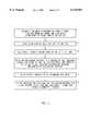
- Step 1provides a metal leadframe.
- the leadframeincludes a rectangular frame, e.g., a square frame.
- a substantially planar die padis within and connected to the frame.
- a plurality of finger-like rectangular tabsextend from the frame toward the die pad without contacting the die pad. The number and location of the tabs around the frame may vary.
- the die pad and the tabshave peripheral side surfaces which include a reentrant portion(s) and asperities. The reentrant position(s) and asperities enhance the connection of the die pad and tabs to the plastic encapsulating material.
- Step 2places and attaches an integrated circuit to a first surface of the die pad.
- Step 3electrically connects a bond wire or an equivalent conductor between each bonding pad of the die and a first surface of one of the tabs.
- Step 4places the leadframe on a flat surface, with the die facing upwards, and applies a viscous encapsulant material onto the upward facing first surface of the leadframe.
- the encapsulant materialis then hardened.
- the encapsulant materialcovers the die, the bond wires, a first surface of the tabs, the first surface of the die pad, the side surfaces of the die pad and tabs, and all or part of the frames around the die pad.
- a lower second surface of the leadframe, including a lower second surface of the die pad and tabs,is not covered with encapsulant.
- Step 5plates the exposed surfaces of the leadframe, including the exposed second surfaces of the die pad and tabs with a metal, such as copper, gold, lead-tin solder, tin, nickel, palladium, or any solderable metal.
- a metalsuch as copper, gold, lead-tin solder, tin, nickel, palladium, or any solderable metal.
- Step 6cuts the encapsulated portions of the leadframe with a saw.
- step 6either obliterates the disposable portions of the leadframe, or severs the disposable portions of the leadframe from other components of the leadframe, such as the die pad and tabs, which are to be included in the package.
- Step 6also trims the encapsulant material and thereby forms the peripheral sides of the package.
- a feature of the packages built by the above described methodis that the die pad and contacts (i.e., the severed tabs of the leadframe) of the package are located at the lower first surface of the package.
- the first surfaces and side surfaces of the die pad and tabsare internal to the package, i.e., covered with encapsulant material, but the second surfaces of the die pad and tabs are not covered by encapsulant material.
- the die pad and tabsare isolated from each other by encapsulant material.
- the encapsulant materialholds the die pad and contacts to the package.
- the connection of the encapsulant material to the die pad and contactsis enhanced by the reentrant portion(s) and asperities of the side surfaces of the die pad and contacts.
- the reentrant portions and asperities of the side surfaces of the die pad and contactsfunction as encapsulant fasteners or lead locks.
- a leadframeis provided which allows a plurality of packages to be constructed simultaneously.
- a leadframe for constructing a plurality of packagessimultaneously includes, for example, a matrix of interconnected rectangular frames.
- a die padis within and connected to each of the interconnected frames.
- a set of tabsextend from each frame toward the sides of the enclosed die pad without contacting the die pad.
- a subsequent encapsulation stepincludes applying an encapsulant material onto the surface of the leadframe to which the dies are attached. This step covers the dies and the side surfaces of the die pads and tabs within a single block of encapsulant material. The encapsulant material is then hardened.
- a cutting stepseparates individual packages from each other and from the disposable portions of the leadframe. The cutting step also severs the connection between each of the interconnected frames and the die pad and tabs within each frame.
- FIG. 1is a flow chart of a method of making a package.
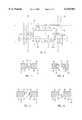
- FIG. 2is a top view of leadframe used for making a package.
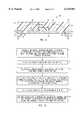
- FIG. 3is an enlarged cross-sectional side view of a circled portion of FIG. 2.
- FIG. 3shows an embodiment of a side surface of a die pad and tab.
- FIG. 4is a first alternative embodiment of a side surface of a die pad and tab.
- FIG. 5is a second alternative embodiment of a side surface of a die pad and tab.
- FIG. 6is a third alternative embodiment of a side surface of a die pad and tab.
- FIG. 7is a top view of the leadframe of FIG. 1 after encapsulation.
- the dashed linesare cutting paths for a subsequent sawing step.
- FIG. 8is a cross-sectional side view of a completed package.
- FIG. 9is a cross-sectional side view of the package of FIG. 8 further including solder interconnection bumps on the package contacts.
- FIG. 10is a flow chart of a method for making a plurality of packages simultaneously.
- FIG. 11is a top view of a leadframe used for making a plurality of packages simultaneously.
- FIG. 1shows an exemplary method of assembling a package in accordance with the present invention.
- FIG. 8shows a completed package.
- FIG. 2is a top view of a first embodiment of a metal leadframe 20 in accordance with the present invention. For ease of view, shading is used in FIG. 2 to distinguish the metal portions of leadframe 20 from empty spaces between the various elements of leadframe 20.
- Leadframe 20 of FIG. 2is planar or substantially planar and is made of a conventional leadframe metal, such as copper or copper alloys, plated copper or plated copper alloys, Alloy 42 (42% nickel, 58% iron), or copper plated steel, depending on the application.
- the opposing upper and lower surfaces of leadframe 20may be plated with different metals.
- the tabs 30 and/ or other portions of leadframe 20 which ultimately are enclosed within the packagemay be plated with silver, gold, nickel palladium, or copper. Such plating, for example, may enhance attachment of bond wires to tabs 30.
- FIG. 2includes dash lines A--A, B--B, C--C, and D--D. These are lines which indicate where leadframe 20 is cut in Step 6 of FIG. 1. Step 6 is described below.
- FIG. 2also includes a circle and dashed line 3--3, which indicate the view of FIG. 3.
- Leadframe 20 of FIG. 2includes a peripheral rectangular frame 21.
- Frame 21consists of four rectilinear members.
- the two intersecting pairs of parallel members of frame 21are denoted as members 22 and 22A and 23 and 23A.
- a rectangular die pad 24is within and connected to frame 21.
- Die pad 24has a planar or substantially planar upper first surface 25 and, although it is not shown in FIG. 2, an opposite planar or substantially planar lower second surface 26.
- Die pad 24also has peripheral side surfaces 27 between upper first surface 25 and lower second surface 26.
- a connector 28connects two parallel side surfaces 27 of die pad 24 to members 22 and 22A of frame 21 of FIG. 2.
- Each connector 28includes a mushroom-shaped anchor 29, although other shapes may be used for anchor 29.
- Three finger-like rectangular tabs 30are connected to and extend from members 23 and 23A toward an adjacent side surface 27 of die pad 24 without contacting side surfaces 27. As a result of this configuration, the completed package will have a single row of three contacts on two parallel sides of the package. Tabs 30 ultimately are severed from members 23 and 23A along cut lines C--C and D--D of FIG. 2, and become the contacts of the package.
- tabs 30may vary. For example, instead of having tabs 30 only on members 23 and 23A of frame 21 of leadframe 20, as in FIG. 2, sets of tabs 30 may be placed on all four members of frame 21. This alternative embodiment would result in the formation of a quad package.
- Each tab 30 of FIG. 2has a planar or substantially planar upper first surface 31 and, although it is not shown in FIG. 2, an opposite planar or substantially planar lower second surface 32. Each tab 30 also has three peripheral side surfaces 33 between upper first surface 31 and lower second surface 32.
- FIGS. 3-6show an enlarged cross-sectional side view of the circled portion of FIG. 2 along line 3--3.
- FIGS. 3-6show, in accordance with the present invention, a side surface 27 of a die pad 24 and a side surface 33 of a tab 30 of leadframe 20 of FIG. 2.
- Side surface 27 of die pad 24 and side surface 33 of tab 30 of FIG. 3have reentrant portions.
- the upper and lower portions of side surfaces 27 and 33are reentrant such that there is a central peak 34 which extends outward from side surfaces 27 and 33 of die pad 24 and tab 30, respectively.
- Encapsulant materialflows into the reentrant portions of side surfaces 27 and 33.
- Central peak 34extends into the encapsulant material.
- the reentrant portions of side surfaces 27 of die pad 24 and side surfaces 33 of tabs 30 of FIG. 3have the function, in a completed package, of enhancing the connection between the encapsulating material, on the one hand, and die pad 24 and the contacts of the package (i.e., severed tabs 30), on the other hand.
- side surface 27 of die pad 24 and side surface 33 of tab 30 of FIG. 3have a roughly-textured surface which includes numerous asperities. Encapsulant material flows into the areas of the asperities. The asperities also enhance the connection between the encapsulant material and die pad 24 and the contacts of the package (i.e., the severed tabs 30).
- FIG. 4shows a first alternative profile for side surfaces 27 of die pad 24 and side surfaces 33 of tabs 30 of leadframe 20 of FIG. 2.
- side surfaces 27 and 33each have a central depression 35 and a roughly-textured surface which includes numerous asperities.
- Encapsulant materialflows into central depression 35 and in the areas of the asperities.
- the reentrant portion and asperities of side surfaces 27 and 33 of FIG. 4have the function, in a completed package, of enhancing the connection between the encapsulant material and die pad 24 and the contacts of the package (i.e., the severed tabs 30).
- FIG. 5shows a second alternative profile for side surfaces 27 of die pad 24 and side surfaces 33 of tabs 30 of leadframe 20 of FIG. 2.
- side surfaces 27 and 33include a rounded lip 36 adjacent to upper surface 25 and 31 of die pad 24 and tab 30, respectively.
- Lip 30has a roughly-textured surface which includes numerous asperities.
- Side surfaces 27 and 33also have a reentrant orthogonal portion 37 beneath lip 3G, adjacent to lower second surface 29 and 32 of die pad 24 and tab 30, respectively.
- Encapsulant materialflows beneath lip 36 and into the area of the asperities.
- the reentrant portions and asperities of side surface 27 of die pad 24 and side surface 33 of tab 30 of FIG. 5have the function, in a completed package, of enhancing the connection between the encapsulant material and die pad 24 and the contacts of the package (i.e., tabs 30 after they are severed from members 23 and 23A).
- FIG. 6shows a third alternative for side surfaces 27 of die pad 24 and side surfaces 33 of tabs 30 of leadframe 20 of FIG. 1.
- side surfaces 27 and 33each include a rectangular lip 38 adjacent to upper surface 25 and 31 of die pad 24 and tab 30, respectively.
- Side surfaces 27 and 33also have a reentrant orthogonal portion 39 beneath lip 38 adjacent to lower second surface 29 and 32 of die pad 24 and tab 30, respectively.
- Encapsulant materialflows beneath lip 38.
- the reentrant portions of side surface 27 of die pad 24 and side surface 33 of tab 30 of FIG. 6have the function, in a completed package, of enhancing the connection between the encapsulant material and die pad 24 and the contacts of the package (i.e., severed tabs 30).
- Step 1 of FIG. 1provides a metal leadframe having features like those shown in FIG. 2 and either FIG. 3, 4, 5, or 6, or equivalents thereof.
- Leadframe 20 of FIG. 2is formed from rolled strip metal stock by wet chemical etching or mechanical stamping using progressive dies.
- chemical etchingis a process that uses photolithography and metal-dissolving chemicals to etch a pattern into a metal strip.
- the photoresistis exposed to ultraviolet light through a photo mask having a desired pattern, and is subsequently developed and cured. Chemicals are sprayed or otherwise applied to the masked strip, and exposed portions of the strip are etched away, leaving the desired pattern.
- progressive stampinguses sets of progressive dies to mechanically remove metal from a metal strip.
- Each of a plurality of stamping stationsuses one of the dies to punch a distinct small area of metal from the strip as the strip moves through the stations.
- a leadframe 20 having side surfaces like FIG. 3can be formed by chemically etching the rolled strip metal stock from both sides using a conventional liquid etchant. The etch process is stopped early so that there is an underetching of all of the side surfaces of the components of leadframe 20, including side surfaces 27 of die pad 24 and side surfaces 33 of tabs 30, compared to the time it would take to form vertical side surfaces.
- the size and shape of central peak 34 of FIG. 2is controlled by the amount of underetching.
- a leadframe 20 having side surfaces like FIG. 4can be formed by chemically etching the rolled strip metal stock from one side using a conventional liquid etchant. The etch process is continued beyond the time required to form orthogonal side surfaces for the components of leadframe 20.
- the size and shape of central depression 35 of FIG. 3is controlled by the amount of overetching.
- a leadframe 20 having side surfaces like FIG. 5can be formed in a two step process.
- the first step of such a processinvolves forming a leadframe 20 by chemical etching or progressive stamping so that the side surfaces of the components of leadframe 20, including die pad 24 and tabs 30, have an orthogonal profile
- the second stepinvolves coining the upper first surface of the leadframe 20, that is, applying a high pressure impact to the upper first surface of the leadframe 20. This step deforms the side surfaces of leadframe 40 adjacent to the impacted surface so that the rounded, asperity-marked protruding lip 36 of FIG. 5 is formed.
- a leadframe 20 having side surfaces like FIG. 6can be formed by progressive stamping.
- the side surfaces of the components of leadframe 20, including side surfaces 27 of die pad 24 and the side surfaces 33 of tabs 30,can be provided with a rectangular lip 38 and a reentrant orthogonal portion 39 by including intermediate stamping steps which do not fully cut through the rolled strip metal stock before finally cutting through the rolled strip sheet.
- the intermediate stamping steps and the final cutting stepscombine to form the rectangular, protruding lips 38 of side surfaces 27 and 33 of FIG. 5.
- Step 2 of FIG. 1places an integrated circuit die onto upper first surface 25 of die pad 24.
- the placement and attachment of the die onto die pad 24may be performed using a conventional die attach machine and conventional die attach adhesives.
- leadframe 20 of FIG. 2is grounded to protect against electrostatic discharge ("ESD").
- Step 3 of FIG. 1electrically connects a conductive metal bond wire between individual bonding pads on the integrated circuit die and the upper first surface 31 of individual tabs 30 on leadframe 20 of FIG. 2. Tabs 30 ultimately become contacts in the completed package, after tabs 30 are severed from members 23 and 23A of frame 21.
- Conventional bond wire attachment equipmentmay be used for Step 3.
- Leadframe 20 of FIG. 2is grounded during this wiring step to prevent damage to the integrated circuit dies due to electrostatic discharge.
- each bonding pad of each dieis electrically connected to a tab 30 of leadframe 20 of FIG. 1, which is grounded. Tabs 30 of leadframe 20 are all shorted together, which facilitates ESD protection.
- Step 4 of FIG. 1the lower second surface of leadframe 20 of FIG. 2 is placed on a flat surface, and a viscous adhesive encapsulating material is applied onto the upward facing upper first surface of leadframe 20.
- the encapsulating materialis applied so that the encapsulating material covers: the integrated circuit die; the bond wires; any exposed peripheral portions of upper first surface 25 of die pad 24 around the die; side surfaces 27 of die pad 24; upper first surface 31 of tabs 30; side surfaces 33 of tabs 33; and part or all of the width of members 22, 22A, 23, and 23A of frame 21.
- the encapsulant materialalso fills the empty spaces between the components within frame 21 of leadframe 20.
- the encapsulant materialdoes not, however, cover lower second surface 26 of die pad 24 or lower second surfaces 32 of tabs 30 of FIG. 2.
- die pad 24may be up set during the encapsulation step so that a thin layer of encapsulant material forms under lower second surface 26 of die pad 24. If such a step were used, die pad 24 would be completely internal to the package. Finally, the encapsulant material is hardened.
- Step 4 of FIG. 1may be accomplished, depending on the application.
- leadframe 20 of FIG. 2is placed on a horizontal surface.
- a contiguous bead of a conventional hardenable viscous adhesive materialsuch as HYSOL 4451 epoxy from the Dexter-Hysol Company of City of Industry, Calif., is applied onto the upper first surface of side members 22, 22A, 23, and 23A of frame 21 of leadframe 20 of FIG. 2, forming a closed rectangular dam.
- the damis solidified, such as by heating at 150° C. for one hour.
- a conventional hardenable viscous adhesive material suitable for encapsulating packagessuch as HYSOL 4450 encapsulant
- HYSOL 4450 encapsulantis applied within the dam so that the incomplete package within the dam is covered with encapsulant material.
- the encapsulant materialis hardened, such as by heating at 150° C. for one hour, forming a single solid block of encapsulant material above and on leadframe 20, including on its side surfaces.
- Step 4 of FIG. 1may be accomplished using conventional plastic molding techniques.
- leadframe 20 of FIG. 2is placed in a mold, and a single block of solid molded encapsulant material is formed above and on leadframe 20, including on its side surfaces.
- the encapsulant materialmay be a conventional plastic molding compound applied using conventional techniques.
- Example molding compoundsinclude NITTO MP-8000AN molding compound from the Nitto Company of Japan, and EME 7351 UT molding compound from the Sumitomo Company of Japan.
- Conventional gatesmay be formed in leadframe 20 to assist in the molding process.
- Step 5 of FIG. 1the portions of leadframe 20 of FIG. 2 which are not covered with the encapsulant material, including lower second surface 26 of die pad 24 and lower second surfaces 32 of tabs 30, are plated using a conventional plating metal compatible with printed circuit boards.
- exposed second surfaces 26 and 33 of die pad 24 and tabs 30, respectivelymay be plated with gold, nickel palladium, inconel, lead tin solder, or tantalum, depending on the application.
- the plating stepis facilitated by the electrical interconnection of the components of leadframe 20.
- FIG. 7is a top view of leadframe 20 of FIG. 2 after the completion of Steps 1-5 of FIG. 1.
- a rectangular block of hardened encapsulant material 40covers the upper first surface of leadframe 20.
- encapsulant material 40also covers side surfaces 27 and 33 of die pad 24 and tabs 30, respectively, of leadframe 20.
- the block of encapsulant material 40 in FIG. 7covers a portion of the width of members 22, 22A, 23, and 23A of frame 21 of leadframe 20.
- the peripheral portions of members 22, 22A, 23, and 23A of frame 21remain exposed.
- encapsulant material 40could be deposited over the entire upper first surface of leadframe 20.
- encapsulant material 40could be deposited within frame 21 so that tabs 30 are covered, but members 22, 22A, 23, and 23A are not covered.
- Step 6 of FIG. 1cuts leadframe 20 of FIG. 7 in situ.
- Step 6severs the connection between tabs 30 and members 23 and 23A of frame 21 of leadframe 20.
- Step 2also severs connectors 28 between die pad 24 and members 22 and 22A of frame 21 of leadframe 20.
- Step 6also cuts encapsulant material 40, forming vertical external side surfaces of the package.
- Step 6completes the formation of the package by cutting a completed package away from the disposable portions of leadframe 20.
- Step 6may be performed using a saw or other shearing apparatus.
- the encapsulated leadframe 20 of FIG. 7is inverted and placed on sticky film.
- a conventional wafer sawis used to saw a completed package from the encapsulated leadframe 20.
- Criss-crossing rectilinear cutsare made along dashed lines A--A, B--B, C--C, and D--D of FIGS. 2 and 7 so that the disposable portions of leadframe 20, including side members 22, 22A, 23, and 23A of frame 21, connectors 28 and anchors 29, are cut away from the package, isolated within encapsulant material 40, or obliterated by the saw.
- the cutting path of the saw and/or the width of the saw bladeshould be selected so that the connections between tabs 30 and members 23 and 23A are severed and side members 22, 22A, 23, and 23A are cut away or obliterated, but all or most of each tab 30 remains intact.
- FIG. 8is a cross-sectional side view of an exemplary package 50 made from leadframe 20 of FIG. 2 according to Steps 1-6 of FIG. 1.
- Package 50has a planar or substantially planar external upper first surface 51, and an opposite planar or substantially planar external lower second surface 52.
- Orthogonal external package sides 57are at the periphery of package 50 between upper first surface 51 and lower second surface 52. Sides 57 were formed during Step 6, when encapsulant material 40 and tabs 30 were cut.
- Lower second surface 52 of package 50 of FIG. 8consists of die pad 24, a plurality of peripheral contacts 53, and hardened encapsulant material 40.
- Die pad 24 and each contact 53are like islands at the lower external second surface 52 of package 50. They are physically separated from each other by encapsulant material 40.
- Die pad 24 and contacts 53 of FIG. 8are vestiges of leadframe 20 of FIG. 2. Referring to FIGS. 2 and 8, contacts 53 of package 50 of FIG. 8 were formed when the connections between tabs 30 and members 23 and 23A were severed by the saw during Step 6.
- Die pad 24 of FIG. 8is rectangular and is located at lower second surface 52 of package 50.
- Die pad 24includes a planar or substantially planar upper first surface 25, an opposite planar or substantially planar second surface 26, and peripheral side surfaces 27.
- Second surface 26 of die pad 24is in the same plane as lower second surface 52 of package 50 in FIG. 8, although in alternative embodiments, die pad 24 may be set up into encapsulant material 40.
- rectangular die pad 24has four side surfaces 27 (only two are shown). Each side surface 27 of die pad 24 has a reentrant portion(s), as exemplified by FIGS. 3-6. In addition, side surface 27 may have asperities, as exemplified by FIGS. 3-5.
- integrated circuit die 56is on and attached to upper first surface 25 of die pad 24. Peripheral portions of upper first surface 25 are covered by encapsulant material 40. Side surfaces 27 of die pad 24 also are covered by encapsulant material 40. Lower second surface 26 of die pad 24 is not covered by encapsulant material 40, but rather is exposed at lower external surface 52 of package 50. In an alternative embodiment (not shown), die pad 24 may be entirely internal to encapsulant material 40 of package 50.
- package 50Two contacts 53 are shown in package 50 of FIG. 8, but since package 50 was constructed from leadframe 20 of FIG. 2, it should be understood that package 50 has a set of three contacts 53 on two sides 57 of package 50. In alternative embodiments, package 50 could be formed with a different number or arrangement of contacts, depending on the application.
- Each contact 53 of FIG. 8has a substantially rectangular perimeter and is located at the lower second surface 52 of package 50.
- Each contact 53includes a planar or substantially planar upper first surface 31, an opposite planar or substantially planar second surface 32, three internal side surfaces 33 (only one is shown in FIG. 8) having reentrant portions, and one external orthogonal side surface 55.
- Second surface 32 of contact 53is in the same plane as lower second surface 52 of package 50.
- First surface 31 and side surfaces 33 of contacts 53are covered with an encapsulant material.
- Second surface 32 and external side surface 55 of contacts 53are not covered with encapsulant material.
- Orthogonal external side surfaces 55 of contacts 53 of FIG. 8were formed during Step 6 of FIG. 1 when the saw cut the connections between tabs 30 and members 23 and 23A of leadframe 20 of FIG. 2. Accordingly, the external side surface 55 of each contact 53 has a vertical profile which is the same plane as the corresponding vertical side 57 of package 50.
- each contact 53has reentrant portions, as exemplified by FIGS. 3-6.
- side surfaces 33may have asperities, as exemplified by FIGS. 3-5. Both the reentrant portion(s) and asperities of contacts 53 enhance the connection between contacts 53 and encapsulant material 40 of package 50 of FIG. 8.
- contacts 53need not be substantially rectangular in shape. For example, if tabs 30 of leadframe 20 of FIG. 2 had a circular perimeter, then contacts 53 would have a largely circular perimeter with a rectilinear portion formed during the cutting of tab 30 from leadframe 20 in Step 6.
- a bond wire 58is connected between each bonding pad 56a of die 56 and the upper first surface 31 of each contact 53. Bond wire 58 electrically connects individual bonding pads 56a of die 56 to individual contacts 53.
- Second surface 32 of contacts 53 of FIG. 8may be directly connected to an external printed circuit board, as in an LCC package.
- a solder interconnection bumpmay be formed on contacts 53 for physically and electrically connecting package 50 to a printed circuit board.
- FIG. 9shows a solder interconnection bump 60 formed on lower second surface 32 and external side surface 55 of each contact 53 of package 50 of FIG. 8.
- second surface 26 of die pad 24also may be connected, such as by solder paste, to the printed circuit board to facilitate package cooling.
- the coolingoccurs by thermal conduction.
- FIG. 10is a flow chart for an alternative assembly method, in accordance with the present invention, for constructing a package like that of FIG. 8.
- a plurality of packagesare constructed simultaneously.
- the basic steps of the FIG. 10 processare the same as the FIG. 1 process.
- Step 1 of FIG. 10provides a thin metal leadframe which includes a plurality of interconnected rectangular frames in a matrix. A die pad is provided within each frame.
- FIG. 11shows an exemplary metal leadframe 70, in accordance with the present invention, suitable for Step 1 of FIG. 10. Shading is used in FIG. 11 to distinguish metal portions of leadframe 70 from empty space between the components of leadframe 70.
- Leadframe 70 of FIG. 11is planar or substantially planar and is formed of metal.
- the metals and methods used for constructing leadframe 70are the same as those described above for leadframe 20 of FIG. 2.
- Leadframe 70 of FIG. 11includes a disposable rectangular outer frame 71.
- Outer frame 71consists of four intersecting members, denoted as members 72-75.
- Member 72is parallel to member 74, and member 73 is parallel to member 75.
- outer frame 71 of FIG. 11are four interconnected rectangular frames in a two by two matrix. These frames are formed by the intersection of three disposable strips 76 and three disposable strips 77. Each of the four interconnected frames of FIG. 11 has the same basic features as frame 21 of FIG. 2. Accordingly, the same reference numbers will be used, where applicable, and associated discussion will be abbreviated.
- a rectangular die pad 24is within and connected to each of the four frames formed by strips 76 and 77 of FIG. 11. As in FIG. 2, each die pad 24 of FIG. 11 has four side surfaces 27. Each side surface 27 has a reentrant portion(s), such as in the examples of FIGS. 3-6. Side surfaces 27 also may include asperities, such as those shown in FIGS. 3-5.
- Three parallel strips 76are within and connected to frame 71 of FIG. 11.
- a first strip 76is adjacent to, parallel to, and connected to member 72 of frame 71.
- a second strip 76is adjacent to, parallel to, and connected to member 74 of frame 71.
- a third strip 76is located in the center of frame 71 between juxtaposed pairs of die pads 24.
- Each strip 76 of FIG. 11is connected to each of the die pads 24 which are adjacent to that particular strip 76.
- a disposable mushroom-shaped anchor 29connects each strip 76 to each adjacent die pad 24.
- Two disposable connectors 78connect member 72 to its adjacent strip 76, and two connectors 78 connect member 74 to its adjacent strip 76. The number and locations of connectors 76 may vary.
- Three parallel strips 77also are within and connected to frame 71 of FIG. 11.
- One strip 77is adjacent to, parallel to, and connected to side members 73 and 75 of frame 71.
- a disposable connector 78connects members 73 and 75 to their respective adjacent strip 77.
- a third strip 77is located in the center of frame 71 between juxtaposed pairs of die pads 24.
- a gate 79extends at approximately a 45 degree angle from each of the four inner corners of frame 71 and connects to the interconnected ends of peripheral strips 76 and 77. Gate 79 is useful for the introduction of molding compound into a mold, where molding is the chosen method of encapsulation.
- Central strip 76 of FIG. 11intersects central strip 77 at the center of leadframe 70.
- the ends of central strips 76 and 77intersect the peripheral strips 77 and 76, respectively.
- a plurality of straight, evenly-spaced, finger-like, rectangular tabs 30extend in sets of five from each strip 77 toward the sides of each of the die pads 24 adjacent that particular strip 77. Tabs 30 do not contact die pads 24.
- the central strip 77 that is between juxtaposed pairs of die pads 24has mirror-image sets of five tabs 30 which extend in opposite directions toward each of the juxtaposed die pads 24. Each tab 30 will ultimately form a contact 53 of package 50 of FIG. 8.
- Each tab 30 of FIG. 11has three side surfaces 33 which have a reentrant portion(s), such as shown in FIGS. 3-6. Side surfaces 33 of tabs 53 also may include asperities, such as those shown in FIGS. 3-5. The reentrant portions and asperities of side surfaces 33 of tabs 30 enhance the connection between encapsulant material 40 and contacts 53 (i.e., severed tabs 30) of a completed package 10 of FIG. 8.
- Step 2 of FIG. 10places and attaches an integrated circuit die 56 on upper first surface 25 of each die pad 24 of leadframe 70 of FIG. 11, as described above for Step 2 of FIG. 1.
- Step 3 of FIG. 10electrically connects a conductive metal bond wire 58 between each bonding pad 56a on each integrated circuit die 56 attached to leadframe 70 and a tab 30.
- Bond wire 58is connected to the first surface 31 of each tab 30.
- the methods for Step 3 of FIG. 11are the same as described above for Step 3 of FIG. 1.
- Step 4 of FIG. 10covers each incomplete package of leadframe 70 of FIG. 11, including all of the dies 56, with a conventional viscous, adhesive encapsulant material.
- the methods and materials used for Step 4 of FIG. 10are the same as for Step 4 of FIG. 1, except that the encapsulant material is applied onto all of the incomplete packages 50 of leadframe 70 of FIG. 11.
- the encapsulant materialcovers the upper first surface of leadframe 70, as well as side surfaces 27 and 33 of die pads 24 and tabs 33, respectively.
- the encapsulant materialis then hardened into a single block which covers all of the incomplete packages of leadframe 70 of FIG. 11, as well as all or part of the width of members 72-75 of frame 71 of leadframe 70.
- the lower second surface of leadframe 70including lower surfaces 26 and 32 of die pads 24 and tabs 30, respectively, is not covered by encapsulant material, but instead remains exposed.
- Step 5 of FIG. 10plates the exposed lower surface of leadframe 70 of FIG. 11, including lower second surfaces 26 and 32 of die pads 24 and tabs 30, respectively, with a conventional plating metal. This step is accomplished as described above for Step 5 of FIG. 1.
- Step 6 of FIG. 10cuts leadframe 70 of FIG. 11 after the encapsulation step.
- Encapsulated leadframe 70is cut in situ, similar to leadframe 20 of FIG. 7.
- the disposable portions of leadframe 70are either severed from the packages, obliterated, or isolated by encapsulant material from the other components of package 50 of FIG. 8.
- the requirements of and methods used for Step 6 of FIG. 10are basically the same as described above for Step 6 of FIG. 1, except that more cuts have to be made because leadframe 70 of FIG. 11 is bigger and has more components than leadframe 20 of FIG. 2.
- Step 6 of FIG. 10severs the connection between tabs 30 and strips 77 of leadframe 70. This cut forms the isolated, individual contacts 53 shown in package 50 of FIG. 8. Step 6 also severs the connection between anchors 29 and strips 76. This cut physically isolates die pads 24 within the encapsulant material. Step 6 also cuts through the single block of encapsulant material formed during Step 4 to form four packages 50 from leadframe 70 of FIG. 11.
- Step 6may be performed using a saw or other cutting apparatus. Where a saw is used for Step 6, the saw is moved along strips 76 and 77 (See FIG. 11). The saw blade used should be wider than strips 76 and 77 of FIG. 11, but narrower than the combined width of central strip 77 and the back-to-back tabs 30. As a result, moving the saw blade along strips 76 and 77 will obliterate strips 76 and 77, but will not obliterate tabs 30. As discussed above, the surface area of tabs 30 must be maintained because the severed tabs 30 become contacts 53 in package 50 of FIG. 8.
- An exemplary method of accomplishing Step 6 of FIG. 10includes a first step of inverting the encapsulated leadframe 70 and placing it on sticky paper. Using the exposed portions of leadframe 70 of FIG. 11 as a pattern, three parallel cuts are made, each of which goes through side members 73 and 75 and along and through the length of a strip 76 of leadframe 70. These three cuts form two of the four external side surfaces 57 of package 50 of FIG. 8; obliterate strips 76; and sever the connections between die pads 24 and strips 76.
- the encapsulated leadframe 70is rotated 90 degrees, and three parallel cuts are made perpendicular to the original three cuts.
- Each of these latter three cutsgoes through side members 72 and 74 and along and through the length of a strip 77.
- These latter three cutsalso form the remaining two external side surfaces 57 of package 50 of FIG. 8. Since the width of the saw blade is selected to be wider than strips 76 and 77, but narrower than the combination of central strip 77 and tabs 30, the latter three cuts obliterate strips 77 but do not obliterate the tabs 30 which are attached to strips 77.
- leadframe 70 of FIG. 11changes can be made to leadframe 70 of FIG. 11 in order to change the size, shape and numbers of the packages 50 (FIG. 7) formed from leadframe 70.
- the size of the leadframemay be adjusted so that two, eight, sixteen, forty-eight or some other number of packages are formed simultaneously.
- onemay multiply the number of packages formed simultaneously by forming several leadframes 70 adjacent to each other on a single strip of rolled stock, and processing all of the leadframes 70 on the strip simultaneously.
- the peripheral shapes of die pads 24 and tabs 30may be changed from rectangular to some other shape.
- profiles of side surfaces 27 and 33 of die pads 24 and tabs 30, respectivelycan be altered from the embodiments of FIGS. 3-6, provided that the function of enhancing the connection between encapsulant material 40 and the die pads 24 and contacts 53 of packages 50 of FIG. 8 is maintained.
- Leadframe 70 of FIG. 11may be modified in other ways as well.
- the peripheral strips 76 and 77 that are adjacent to members 72-75may be omitted.
- the anchors 29 of FIG. 11would be attached to members 72 and 74, and tabs 30 would be attached to members 73 and 75 of frame 71 of leadframe 70.
- a mold having individualized cavities for forming a block of encapsulant material above each the four interconnected frames and die pads 24 of leadframe 70may be used. In such a case, less encapsulant material would be cut in Step 6 of FIG. 10.
Landscapes
- Engineering & Computer Science (AREA)
- Physics & Mathematics (AREA)
- Computer Hardware Design (AREA)
- Microelectronics & Electronic Packaging (AREA)
- Power Engineering (AREA)
- Condensed Matter Physics & Semiconductors (AREA)
- General Physics & Mathematics (AREA)
- Geometry (AREA)
- Manufacturing & Machinery (AREA)
- Lead Frames For Integrated Circuits (AREA)
- Structures Or Materials For Encapsulating Or Coating Semiconductor Devices Or Solid State Devices (AREA)
Abstract
Description
Claims (19)
Priority Applications (22)
| Application Number | Priority Date | Filing Date | Title |
|---|---|---|---|
| US09/103,760US6143981A (en) | 1998-06-24 | 1998-06-24 | Plastic integrated circuit package and method and leadframe for making the package |
| KR1020007001533AKR20010022928A (en) | 1998-06-24 | 1999-06-14 | Plastic integrated circuit package and method and leadframe for making the package |
| EP99928630AEP1016138A1 (en) | 1998-06-24 | 1999-06-14 | Plastic integrated circuit package and method and leadframe for making the package |
| JP2000556398AJP2002519848A (en) | 1998-06-24 | 1999-06-14 | Integrated circuit plastic package, method of forming the same, and lead frame for forming the package |
| PCT/US1999/013364WO1999067821A1 (en) | 1998-06-24 | 1999-06-14 | Plastic integrated circuit package and method and leadframe for making the package |
| CA002298695ACA2298695A1 (en) | 1998-06-24 | 1999-06-14 | Plastic integrated circuit package and method and leadframe for making the package |
| US09/615,107US6433277B1 (en) | 1998-06-24 | 2000-07-13 | Plastic integrated circuit package and method and leadframe for making the package |
| US10/007,337US6684496B2 (en) | 1998-06-24 | 2001-10-22 | Method of making an integrated circuit package |
| US10/119,826US20020108769A1 (en) | 1998-06-24 | 2002-04-11 | Plastic integrated circuit package and method and lead frame for making the package |
| US10/156,889US20020144396A1 (en) | 1998-06-24 | 2002-05-30 | Method of making an integrated circuit package |
| US10/171,702US6630728B2 (en) | 1998-06-24 | 2002-06-14 | Plastic integrated circuit package and leadframe for making the package |
| US10/626,150US7071541B1 (en) | 1998-06-24 | 2003-07-24 | Plastic integrated circuit package and method and leadframe for making the package |
| US10/688,710US6893900B1 (en) | 1998-06-24 | 2003-10-17 | Method of making an integrated circuit package |
| US10/847,742US7005326B1 (en) | 1998-06-24 | 2004-05-18 | Method of making an integrated circuit package |
| US11/021,340US7030474B1 (en) | 1998-06-24 | 2004-12-22 | Plastic integrated circuit package and method and leadframe for making the package |
| US11/299,859US7112474B1 (en) | 1998-06-24 | 2005-12-12 | Method of making an integrated circuit package |
| US11/503,752US7332375B1 (en) | 1998-06-24 | 2006-08-14 | Method of making an integrated circuit package |
| US11/970,712US7560804B1 (en) | 1998-06-24 | 2008-01-08 | Integrated circuit package and method of making the same |
| US13/009,690US8318287B1 (en) | 1998-06-24 | 2011-01-19 | Integrated circuit package and method of making the same |
| US13/662,702US8853836B1 (en) | 1998-06-24 | 2012-10-29 | Integrated circuit package and method of making the same |
| US14/142,457US8963301B1 (en) | 1998-06-24 | 2013-12-27 | Integrated circuit package and method of making the same |
| US14/592,648US9224676B1 (en) | 1998-06-24 | 2015-01-08 | Integrated circuit package and method of making the same |
Applications Claiming Priority (1)
| Application Number | Priority Date | Filing Date | Title |
|---|---|---|---|
| US09/103,760US6143981A (en) | 1998-06-24 | 1998-06-24 | Plastic integrated circuit package and method and leadframe for making the package |
Related Child Applications (2)
| Application Number | Title | Priority Date | Filing Date |
|---|---|---|---|
| US39301699ADivision | 1998-06-24 | 1999-09-10 | |
| US09/615,107ContinuationUS6433277B1 (en) | 1998-06-24 | 2000-07-13 | Plastic integrated circuit package and method and leadframe for making the package |
Publications (1)
| Publication Number | Publication Date |
|---|---|
| US6143981Atrue US6143981A (en) | 2000-11-07 |
Family
ID=22296901
Family Applications (10)
| Application Number | Title | Priority Date | Filing Date |
|---|---|---|---|
| US09/103,760Expired - LifetimeUS6143981A (en) | 1998-06-24 | 1998-06-24 | Plastic integrated circuit package and method and leadframe for making the package |
| US09/615,107Expired - LifetimeUS6433277B1 (en) | 1998-06-24 | 2000-07-13 | Plastic integrated circuit package and method and leadframe for making the package |
| US10/007,337Expired - LifetimeUS6684496B2 (en) | 1998-06-24 | 2001-10-22 | Method of making an integrated circuit package |
| US10/119,826AbandonedUS20020108769A1 (en) | 1998-06-24 | 2002-04-11 | Plastic integrated circuit package and method and lead frame for making the package |
| US10/156,889AbandonedUS20020144396A1 (en) | 1998-06-24 | 2002-05-30 | Method of making an integrated circuit package |
| US10/171,702Expired - LifetimeUS6630728B2 (en) | 1998-06-24 | 2002-06-14 | Plastic integrated circuit package and leadframe for making the package |
| US13/009,690Expired - Fee RelatedUS8318287B1 (en) | 1998-06-24 | 2011-01-19 | Integrated circuit package and method of making the same |
| US13/662,702Expired - Fee RelatedUS8853836B1 (en) | 1998-06-24 | 2012-10-29 | Integrated circuit package and method of making the same |
| US14/142,457Expired - Fee RelatedUS8963301B1 (en) | 1998-06-24 | 2013-12-27 | Integrated circuit package and method of making the same |
| US14/592,648Expired - Fee RelatedUS9224676B1 (en) | 1998-06-24 | 2015-01-08 | Integrated circuit package and method of making the same |
Family Applications After (9)
| Application Number | Title | Priority Date | Filing Date |
|---|---|---|---|
| US09/615,107Expired - LifetimeUS6433277B1 (en) | 1998-06-24 | 2000-07-13 | Plastic integrated circuit package and method and leadframe for making the package |
| US10/007,337Expired - LifetimeUS6684496B2 (en) | 1998-06-24 | 2001-10-22 | Method of making an integrated circuit package |
| US10/119,826AbandonedUS20020108769A1 (en) | 1998-06-24 | 2002-04-11 | Plastic integrated circuit package and method and lead frame for making the package |
| US10/156,889AbandonedUS20020144396A1 (en) | 1998-06-24 | 2002-05-30 | Method of making an integrated circuit package |
| US10/171,702Expired - LifetimeUS6630728B2 (en) | 1998-06-24 | 2002-06-14 | Plastic integrated circuit package and leadframe for making the package |
| US13/009,690Expired - Fee RelatedUS8318287B1 (en) | 1998-06-24 | 2011-01-19 | Integrated circuit package and method of making the same |
| US13/662,702Expired - Fee RelatedUS8853836B1 (en) | 1998-06-24 | 2012-10-29 | Integrated circuit package and method of making the same |
| US14/142,457Expired - Fee RelatedUS8963301B1 (en) | 1998-06-24 | 2013-12-27 | Integrated circuit package and method of making the same |
| US14/592,648Expired - Fee RelatedUS9224676B1 (en) | 1998-06-24 | 2015-01-08 | Integrated circuit package and method of making the same |
Country Status (6)
| Country | Link |
|---|---|
| US (10) | US6143981A (en) |
| EP (1) | EP1016138A1 (en) |
| JP (1) | JP2002519848A (en) |
| KR (1) | KR20010022928A (en) |
| CA (1) | CA2298695A1 (en) |
| WO (1) | WO1999067821A1 (en) |
Cited By (268)
| Publication number | Priority date | Publication date | Assignee | Title |
|---|---|---|---|---|
| US6284570B1 (en) | 1998-12-28 | 2001-09-04 | Semiconductor Components Industries Llc | Method of manufacturing a semiconductor component from a conductive substrate containing a plurality of vias |
| US6309909B1 (en)* | 1998-07-02 | 2001-10-30 | Mitsubishi Denki Kabushiki Kaisha | Semiconductor device and method of manufacturing the same |
| US6342406B1 (en) | 2000-11-15 | 2002-01-29 | Amkor Technology, Inc. | Flip chip on glass image sensor package fabrication method |
| US20020020907A1 (en)* | 2000-03-25 | 2002-02-21 | Amkor Technology, Inc. | Semiconductor package |
| US6420779B1 (en)* | 1999-09-14 | 2002-07-16 | St Assembly Test Services Ltd. | Leadframe based chip scale package and method of producing the same |
| US6420204B2 (en) | 1999-06-03 | 2002-07-16 | Amkor Technology, Inc. | Method of making a plastic package for an optical integrated circuit device |
| US20020093093A1 (en)* | 2001-01-15 | 2002-07-18 | Jong Sik Paek | Semiconductor package with stacked dies |
| US20020093087A1 (en)* | 2001-01-15 | 2002-07-18 | Paek Jong Sik | Semiconductor package with stacked dies |
| US6424031B1 (en) | 2000-05-08 | 2002-07-23 | Amkor Technology, Inc. | Stackable package with heat sink |
| US20020105063A1 (en)* | 2000-09-13 | 2002-08-08 | Huat Lee Kock | Stress-free lead frame |
| US6433277B1 (en) | 1998-06-24 | 2002-08-13 | Amkor Technology, Inc. | Plastic integrated circuit package and method and leadframe for making the package |
| US6437429B1 (en) | 2001-05-11 | 2002-08-20 | Walsin Advanced Electronics Ltd | Semiconductor package with metal pads |
| US6448633B1 (en) | 1998-11-20 | 2002-09-10 | Amkor Technology, Inc. | Semiconductor package and method of making using leadframe having lead locks to secure leads to encapsulant |
| US20020125562A1 (en)* | 2000-03-27 | 2002-09-12 | Crowley Sean T. | Attaching semiconductor dies to substrates with conductive straps |
| US6455356B1 (en)* | 1998-10-21 | 2002-09-24 | Amkor Technology | Methods for moding a leadframe in plastic integrated circuit devices |
| US20020149091A1 (en)* | 2001-04-16 | 2002-10-17 | Palmteer William James | Leadframe-based chip scale package |
| US6469369B1 (en) | 1999-06-30 | 2002-10-22 | Amkor Technology, Inc. | Leadframe having a mold inflow groove and method for making |
| US6476478B1 (en) | 1999-11-12 | 2002-11-05 | Amkor Technology, Inc. | Cavity semiconductor package with exposed leads and die pad |
| US6475827B1 (en) | 1999-10-15 | 2002-11-05 | Amkor Technology, Inc. | Method for making a semiconductor package having improved defect testing and increased production yield |
| US6483178B1 (en)* | 2000-07-14 | 2002-11-19 | Siliconware Precision Industries Co., Ltd. | Semiconductor device package structure |
| US6501161B1 (en) | 1999-10-15 | 2002-12-31 | Amkor Technology, Inc. | Semiconductor package having increased solder joint strength |
| US6501156B1 (en)* | 1999-09-10 | 2002-12-31 | Matsushita Electric Industrial Co., Ltd. | Lead frame which includes a die pad, a support lead, and inner leads |
| US6518659B1 (en) | 2000-05-08 | 2003-02-11 | Amkor Technology, Inc. | Stackable package having a cavity and a lid for an electronic device |
| US6525405B1 (en)* | 2000-03-30 | 2003-02-25 | Alphatec Holding Company Limited | Leadless semiconductor product packaging apparatus having a window lid and method for packaging |
| US6525406B1 (en)* | 1999-10-15 | 2003-02-25 | Amkor Technology, Inc. | Semiconductor device having increased moisture path and increased solder joint strength |
| US20030075786A1 (en)* | 2001-10-22 | 2003-04-24 | Fairchild Semiconductor Corporation | Thin, thermally enhanced flip chip in a leaded molded package |
| US6555899B1 (en) | 1999-10-15 | 2003-04-29 | Amkor Technology, Inc. | Semiconductor package leadframe assembly and method of manufacture |
| US6571466B1 (en) | 2000-03-27 | 2003-06-03 | Amkor Technology, Inc. | Flip chip image sensor package fabrication method |
| US6577012B1 (en) | 2001-08-13 | 2003-06-10 | Amkor Technology, Inc. | Laser defined pads for flip chip on leadframe package |
| US20030111719A1 (en)* | 2001-12-19 | 2003-06-19 | Martin Reiss | Electronic device and leadframe and methods for producing the electronic device and the leadframe |
| US6586677B2 (en) | 1999-08-25 | 2003-07-01 | Amkor Technology, Inc. | Plastic integrated circuit device package having exposed lead surface |
| US6589814B1 (en) | 1998-04-02 | 2003-07-08 | National Semiconductor Corporation | Lead frame chip scale package |
| US6593545B1 (en) | 2001-08-13 | 2003-07-15 | Amkor Technology, Inc. | Laser defined pads for flip chip on leadframe package fabrication method |
| US6605865B2 (en) | 2001-03-19 | 2003-08-12 | Amkor Technology, Inc. | Semiconductor package with optimized leadframe bonding strength |
| US6605866B1 (en) | 1999-12-16 | 2003-08-12 | Amkor Technology, Inc. | Stackable semiconductor package and method for manufacturing same |
| US6608366B1 (en) | 2002-04-15 | 2003-08-19 | Harry J. Fogelson | Lead frame with plated end leads |
| US6611047B2 (en) | 2001-10-12 | 2003-08-26 | Amkor Technology, Inc. | Semiconductor package with singulation crease |
| US20030160307A1 (en)* | 2002-02-25 | 2003-08-28 | Rf Micro Devices, Inc. | Leadframe inductors |
| US6614102B1 (en) | 2001-05-04 | 2003-09-02 | Amkor Technology, Inc. | Shielded semiconductor leadframe package |
| US6616436B1 (en) | 1999-10-15 | 2003-09-09 | Amkor Technology, Inc. | Apparatus for manufacturing semiconductor packages |
| US20030178719A1 (en)* | 2002-03-22 | 2003-09-25 | Combs Edward G. | Enhanced thermal dissipation integrated circuit package and method of manufacturing enhanced thermal dissipation integrated circuit package |
| US6627976B1 (en) | 1999-10-15 | 2003-09-30 | Amkor Technology, Inc. | Leadframe for semiconductor package and mold for molding the same |
| US6627977B1 (en) | 2002-05-09 | 2003-09-30 | Amkor Technology, Inc. | Semiconductor package including isolated ring structure |
| US6627864B1 (en)* | 1999-11-22 | 2003-09-30 | Amkor Technology, Inc. | Thin image sensor package |
| US6630726B1 (en) | 2001-11-07 | 2003-10-07 | Amkor Technology, Inc. | Power semiconductor package with strap |
| US6639308B1 (en) | 1999-12-16 | 2003-10-28 | Amkor Technology, Inc. | Near chip size semiconductor package |
| US6646339B1 (en) | 1999-10-15 | 2003-11-11 | Amkor Technology, Inc. | Thin and heat radiant semiconductor package and method for manufacturing |
| US6661083B2 (en) | 2001-02-27 | 2003-12-09 | Chippac, Inc | Plastic semiconductor package |
| US6667544B1 (en) | 2000-06-30 | 2003-12-23 | Amkor Technology, Inc. | Stackable package having clips for fastening package and tool for opening clips |
| US20030234454A1 (en)* | 2002-06-24 | 2003-12-25 | Serafin Pedron | Integrated circuit package and method of manufacturing the integrated circuit package |
| US6677663B1 (en) | 1999-12-30 | 2004-01-13 | Amkor Technology, Inc. | End grid array semiconductor package |
| US6677672B2 (en) | 2002-04-26 | 2004-01-13 | Semiconductor Components Industries Llc | Structure and method of forming a multiple leadframe semiconductor device |
| US6677662B1 (en)* | 1999-10-15 | 2004-01-13 | Amkor Technology, Inc. | Clamp and heat block assembly for wire bonding a semiconductor package assembly |
| US6686651B1 (en) | 2001-11-27 | 2004-02-03 | Amkor Technology, Inc. | Multi-layer leadframe structure |
| US6696747B1 (en) | 1999-10-15 | 2004-02-24 | Amkor Technology, Inc. | Semiconductor package having reduced thickness |
| US6700187B2 (en) | 2001-03-27 | 2004-03-02 | Amkor Technology, Inc. | Semiconductor package and method for manufacturing the same |
| GB2392778A (en)* | 2002-09-04 | 2004-03-10 | Atlantic Technology | Quad flat pack terminals |
| US6707168B1 (en) | 2001-05-04 | 2004-03-16 | Amkor Technology, Inc. | Shielded semiconductor package with single-sided substrate and method for making the same |
| US20040053447A1 (en)* | 2001-06-29 | 2004-03-18 | Foster Donald Craig | Leadframe having fine pitch bond fingers formed using laser cutting method |
| US6713322B2 (en) | 2001-03-27 | 2004-03-30 | Amkor Technology, Inc. | Lead frame for semiconductor package |
| US20040063240A1 (en)* | 2002-09-30 | 2004-04-01 | Fairchild Semiconductor Corporation | Semiconductor die package including drain clip |
| US6730544B1 (en) | 1999-12-20 | 2004-05-04 | Amkor Technology, Inc. | Stackable semiconductor package and method for manufacturing same |
| US6750545B1 (en) | 2003-02-28 | 2004-06-15 | Amkor Technology, Inc. | Semiconductor package capable of die stacking |
| US6753597B1 (en) | 1999-12-16 | 2004-06-22 | Amkor Technology, Inc. | Encapsulated semiconductor package including chip paddle and leads |
| US20040119146A1 (en)* | 2002-09-26 | 2004-06-24 | Seiko Epson Corporation | Semiconductor device and method of manufacturing the same, circuit board, and electronic instrument |
| US6756658B1 (en) | 2001-04-06 | 2004-06-29 | Amkor Technology, Inc. | Making two lead surface mounting high power microleadframe semiconductor packages |
| US6759737B2 (en) | 2000-03-25 | 2004-07-06 | Amkor Technology, Inc. | Semiconductor package including stacked chips with aligned input/output pads |
| US20040142505A1 (en)* | 2003-01-21 | 2004-07-22 | Siliconware Precision Industries Co., Ltd. | Semiconductor package free of substrate and fabrication method thereof |
| US6777265B2 (en) | 2002-04-29 | 2004-08-17 | Advanced Interconnect Technologies Limited | Partially patterned lead frames and methods of making and using the same in semiconductor packaging |
| US6777789B1 (en) | 2001-03-20 | 2004-08-17 | Amkor Technology, Inc. | Mounting for a package containing a chip |
| US20040164430A1 (en)* | 2002-12-20 | 2004-08-26 | Noriaki Sakamoto | Circuit device and method of manufacture thereof |
| US20040169271A1 (en)* | 2002-12-20 | 2004-09-02 | Yusuke Igarashi | Circuit device and method of manufacture thereof |
| US6790710B2 (en) | 2002-01-31 | 2004-09-14 | Asat Limited | Method of manufacturing an integrated circuit package |
| US6794738B2 (en) | 2002-09-23 | 2004-09-21 | Texas Instruments Incorporated | Leadframe-to-plastic lock for IC package |
| US6794740B1 (en) | 2003-03-13 | 2004-09-21 | Amkor Technology, Inc. | Leadframe package for semiconductor devices |
| US6798046B1 (en) | 2002-01-22 | 2004-09-28 | Amkor Technology, Inc. | Semiconductor package including ring structure connected to leads with vertically downset inner ends |
| US6798047B1 (en)* | 2002-12-26 | 2004-09-28 | Amkor Technology, Inc. | Pre-molded leadframe |
| US6803645B2 (en) | 2000-12-29 | 2004-10-12 | Amkor Technology, Inc. | Semiconductor package including flip chip |
| US20040201080A1 (en)* | 2003-04-08 | 2004-10-14 | Suresh Basoor | Leadless leadframe electronic package and IR transceiver incorporating same |
| US6806789B2 (en) | 2002-01-22 | 2004-10-19 | M/A-Com Corporation | Quadrature hybrid and improved vector modulator in a chip scale package using same |
| US20040207052A1 (en)* | 2002-08-30 | 2004-10-21 | Rajeev Joshi | Substrate based unmolded package |
| US20040207054A1 (en)* | 2003-04-21 | 2004-10-21 | Motorola, Inc. | Semiconductor component for electrical coupling to a substrate, and method of manufacturing same |
| US20040217450A1 (en)* | 2003-05-02 | 2004-11-04 | Siliconware Precision Industries Co., Ltd. | Leadframe-based non-leaded semiconductor package and method of fabricating the same |
| US6818973B1 (en) | 2002-09-09 | 2004-11-16 | Amkor Technology, Inc. | Exposed lead QFP package fabricated through the use of a partial saw process |
| US20040252287A1 (en)* | 2003-06-11 | 2004-12-16 | Michael Binnard | Reaction frame assembly that functions as a reaction mass |
| US6841414B1 (en) | 2002-06-19 | 2005-01-11 | Amkor Technology, Inc. | Saw and etch singulation method for a chip package |
| US20050006730A1 (en)* | 2003-07-07 | 2005-01-13 | Motorola, Inc. | Semiconductor component and method of manufacturing same |
| US20050006737A1 (en)* | 2002-04-29 | 2005-01-13 | Shafidul Islam | Partially patterned lead frames and methods of making and using the same in semiconductor packaging |
| US6847103B1 (en) | 1999-11-09 | 2005-01-25 | Amkor Technology, Inc. | Semiconductor package with exposed die pad and body-locking leadframe |
| US6849916B1 (en) | 2000-11-15 | 2005-02-01 | Amkor Technology, Inc. | Flip chip on glass sensor package |
| US6853059B1 (en) | 1999-10-15 | 2005-02-08 | Amkor Technology, Inc. | Semiconductor package having improved adhesiveness and ground bonding |
| US6858474B1 (en)* | 2003-12-01 | 2005-02-22 | Agilent Technologies, Inc. | Wire bond package and packaging method |
| US20050051859A1 (en)* | 2001-10-25 | 2005-03-10 | Amkor Technology, Inc. | Look down image sensor package |
| US6867071B1 (en) | 2002-07-12 | 2005-03-15 | Amkor Technology, Inc. | Leadframe including corner leads and semiconductor package using same |
| US6873032B1 (en) | 2001-04-04 | 2005-03-29 | Amkor Technology, Inc. | Thermally enhanced chip scale lead on chip semiconductor package and method of making same |
| US20050073039A1 (en)* | 2003-10-07 | 2005-04-07 | Rohm Co., Ltd. | Semiconductor device and method of fabricating the same |
| US6879034B1 (en) | 2003-05-01 | 2005-04-12 | Amkor Technology, Inc. | Semiconductor package including low temperature co-fired ceramic substrate |
| US6885086B1 (en) | 2002-03-05 | 2005-04-26 | Amkor Technology, Inc. | Reduced copper lead frame for saw-singulated chip package |
| US6894376B1 (en)* | 2003-06-09 | 2005-05-17 | National Semiconductor Corporation | Leadless microelectronic package and a method to maximize the die size in the package |
| US6893900B1 (en) | 1998-06-24 | 2005-05-17 | Amkor Technology, Inc. | Method of making an integrated circuit package |
| US20050104169A1 (en)* | 2000-09-13 | 2005-05-19 | Carsem Semiconductor Sdn. Bhd. | Stress-free lead frame |
| US20050104174A1 (en)* | 2003-10-06 | 2005-05-19 | Ichiro Kishimoto | Method of fabricating lead frame and method of fabricating semiconductor device using the same, and semiconductor device and portable apparatus and electronic apparatus comprising the same |
| US6897550B1 (en) | 2003-06-11 | 2005-05-24 | Amkor Technology, Inc. | Fully-molded leadframe stand-off feature |
| US6911718B1 (en) | 2003-07-03 | 2005-06-28 | Amkor Technology, Inc. | Double downset double dambar suspended leadframe |
| US6910635B1 (en) | 2002-10-08 | 2005-06-28 | Amkor Technology, Inc. | Die down multi-media card and method of making same |
| US20050146057A1 (en)* | 2003-12-31 | 2005-07-07 | Khor Ah L. | Micro lead frame package having transparent encapsulant |
| US6919620B1 (en) | 2002-09-17 | 2005-07-19 | Amkor Technology, Inc. | Compact flash memory card with clamshell leadframe |
| US6921967B2 (en) | 2003-09-24 | 2005-07-26 | Amkor Technology, Inc. | Reinforced die pad support structure |
| US6927483B1 (en) | 2003-03-07 | 2005-08-09 | Amkor Technology, Inc. | Semiconductor package exhibiting efficient lead placement |
| US20050184368A1 (en)* | 2003-01-21 | 2005-08-25 | Huang Chien P. | Semiconductor package free of substrate and fabrication method thereof |
| US20050189659A1 (en)* | 2003-01-21 | 2005-09-01 | Huang Chien P. | Semiconductor package free of substrate and fabrication method thereof |
| US20050194667A1 (en)* | 2003-01-21 | 2005-09-08 | Siliconware Precision Industries Co., Ltd. | Semiconductor package free of substrate and fabrication method thereof |
| US20050194666A1 (en)* | 2003-01-21 | 2005-09-08 | Huang Chien P. | Semiconductor package free of substrate and fabrication method thereof |
| US20050194665A1 (en)* | 2003-01-21 | 2005-09-08 | Huang Chien P. | Semiconductor package free of substrate and fabrication method thereof |
| WO2005091353A1 (en)* | 2004-02-26 | 2005-09-29 | Infineon Technologies Ag | A non-leaded semiconductor package and a method to assemble the same |
| US20050218300A1 (en)* | 2004-04-02 | 2005-10-06 | Quinones Maria Clemens Y | Surface mount multi-channel optocoupler |
| US6965159B1 (en) | 2001-09-19 | 2005-11-15 | Amkor Technology, Inc. | Reinforced lead-frame assembly for interconnecting circuits within a circuit module |
| US20050255634A1 (en)* | 2004-05-11 | 2005-11-17 | Gem Services, Inc. | Chemical-enhanced package singulation process |
| US6967395B1 (en) | 2001-03-20 | 2005-11-22 | Amkor Technology, Inc. | Mounting for a package containing a chip |
| US20050260795A1 (en)* | 2004-05-24 | 2005-11-24 | Advanced Semiconductor Engineering, Inc. | Method for fabricating leadless packages with mold locking characteristics |
| US20050258520A1 (en)* | 2004-05-18 | 2005-11-24 | Dolan Douglas E | Packaged integrated circuit with MLP leadframe and method of making same |
| US6977431B1 (en)* | 2003-11-05 | 2005-12-20 | Amkor Technology, Inc. | Stackable semiconductor package and manufacturing method thereof |
| US20060001130A1 (en)* | 2002-09-25 | 2006-01-05 | Shafidul Islam | Taped lead frames and methods of making and using the same in semiconductor packaging |
| US7001799B1 (en) | 2003-03-13 | 2006-02-21 | Amkor Technology, Inc. | Method of making a leadframe for semiconductor devices |
| US7005326B1 (en) | 1998-06-24 | 2006-02-28 | Amkor Technology, Inc. | Method of making an integrated circuit package |
| US7008825B1 (en) | 2003-05-27 | 2006-03-07 | Amkor Technology, Inc. | Leadframe strip having enhanced testability |
| US7030474B1 (en) | 1998-06-24 | 2006-04-18 | Amkor Technology, Inc. | Plastic integrated circuit package and method and leadframe for making the package |
| US7042068B2 (en) | 2000-04-27 | 2006-05-09 | Amkor Technology, Inc. | Leadframe and semiconductor package made using the leadframe |
| US20060097366A1 (en)* | 2003-07-19 | 2006-05-11 | Ns Electronics Bangkok (1993) Ltd. | Semiconductor package including leadframe roughened with chemical etchant to prevent separation between leadframe and molding compound |
| US7045883B1 (en) | 2001-04-04 | 2006-05-16 | Amkor Technology, Inc. | Thermally enhanced chip scale lead on chip semiconductor package and method of making same |
| US20060105502A1 (en)* | 2004-11-12 | 2006-05-18 | Advanced Semiconductor Engineering Inc. | Assembly process |
| US7057268B1 (en) | 2004-01-27 | 2006-06-06 | Amkor Technology, Inc. | Cavity case with clip/plug for use on multi-media card |
| US7064009B1 (en) | 2001-04-04 | 2006-06-20 | Amkor Technology, Inc. | Thermally enhanced chip scale lead on chip semiconductor package and method of making same |
| US7071541B1 (en)* | 1998-06-24 | 2006-07-04 | Amkor Technology, Inc. | Plastic integrated circuit package and method and leadframe for making the package |
| US7074654B1 (en) | 2004-04-21 | 2006-07-11 | Amkor Technology, Inc. | Tape supported memory card leadframe structure |
| US20060154404A1 (en)* | 1998-12-11 | 2006-07-13 | Corisis David J | Die paddle clamping method for wire bond enhancement |
| US7091594B1 (en) | 2004-01-28 | 2006-08-15 | Amkor Technology, Inc. | Leadframe type semiconductor package having reduced inductance and its manufacturing method |
| US7095103B1 (en) | 2003-05-01 | 2006-08-22 | Amkor Technology, Inc. | Leadframe based memory card |
| US7095621B2 (en) | 2003-02-24 | 2006-08-22 | Avago Technologies Sensor Ip (Singapore) Pte. Ltd. | Leadless leadframe electronic package and sensor module incorporating same |
| US7102216B1 (en) | 2001-08-17 | 2006-09-05 | Amkor Technology, Inc. | Semiconductor package and leadframe with horizontal leads spaced in the vertical direction and method of making |
| US7102208B1 (en) | 1999-10-15 | 2006-09-05 | Amkor Technology, Inc. | Leadframe and semiconductor package with improved solder joint strength |
| US7112474B1 (en) | 1998-06-24 | 2006-09-26 | Amkor Technology, Inc. | Method of making an integrated circuit package |
| US7112875B1 (en) | 2005-02-17 | 2006-09-26 | Amkor Technology, Inc. | Secure digital memory card using land grid array structure |
| US20060214271A1 (en)* | 2005-03-23 | 2006-09-28 | Jeremy Loraine | Device and applications for passive RF components in leadframes |
| US7122406B1 (en) | 2004-01-02 | 2006-10-17 | Gem Services, Inc. | Semiconductor device package diepad having features formed by electroplating |
| US7138707B1 (en) | 2003-10-21 | 2006-11-21 | Amkor Technology, Inc. | Semiconductor package including leads and conductive posts for providing increased functionality |
| US20060278964A1 (en)* | 2005-06-08 | 2006-12-14 | Psi Technologies, Inc. | Plastic integrated circuit package, leadframe and method for use in making the package |
| US20070001278A1 (en)* | 2005-06-30 | 2007-01-04 | Oseob Jeon | Semiconductor die package and method for making the same |
| US20070052076A1 (en)* | 2002-04-29 | 2007-03-08 | Ramos Mary J | Partially Patterned Lead Frames and Methods of Making and Using the Same in Semiconductor Packaging |
| US7190062B1 (en) | 2004-06-15 | 2007-03-13 | Amkor Technology, Inc. | Embedded leadframe semiconductor package |
| US7192807B1 (en) | 2002-11-08 | 2007-03-20 | Amkor Technology, Inc. | Wafer level package and fabrication method |
| US7193305B1 (en) | 2004-11-03 | 2007-03-20 | Amkor Technology, Inc. | Memory card ESC substrate insert |
| US20070063336A1 (en)* | 2005-09-16 | 2007-03-22 | Hase Andreas A | QFN/SON-compatible package |
| US7201327B1 (en) | 2004-10-18 | 2007-04-10 | Amkor Technology, Inc. | Memory card and its manufacturing method |
| US7202554B1 (en) | 2004-08-19 | 2007-04-10 | Amkor Technology, Inc. | Semiconductor package and its manufacturing method |
| US7211879B1 (en) | 2003-11-12 | 2007-05-01 | Amkor Technology, Inc. | Semiconductor package with chamfered corners and method of manufacturing the same |
| US7214326B1 (en) | 2003-11-07 | 2007-05-08 | Amkor Technology, Inc. | Increased capacity leadframe and semiconductor package using the same |
| US7217991B1 (en) | 2004-10-22 | 2007-05-15 | Amkor Technology, Inc. | Fan-in leadframe semiconductor package |
| US7220915B1 (en) | 2005-02-17 | 2007-05-22 | Amkor Technology, Inc. | Memory card and its manufacturing method |
| US7221433B2 (en) | 2004-01-28 | 2007-05-22 | Nikon Corporation | Stage assembly including a reaction assembly having a connector assembly |
| US20070132073A1 (en)* | 2005-12-09 | 2007-06-14 | Tiong Toong T | Device and method for assembling a top and bottom exposed packaged semiconductor |
| US7245007B1 (en) | 2003-09-18 | 2007-07-17 | Amkor Technology, Inc. | Exposed lead interposer leadframe package |
| US7253503B1 (en) | 1999-11-05 | 2007-08-07 | Amkor Technology, Inc. | Integrated circuit device packages and substrates for making the packages |
| US20070270040A1 (en)* | 2006-05-05 | 2007-11-22 | Jang Sang J | Chamfered Memory Card |
| CN100355066C (en)* | 2003-09-01 | 2007-12-12 | 恩益禧电子股份有限公司 | Leadless type semiconductor package, and production process for manufacturing such leadless type semiconductor package |
| US7332375B1 (en) | 1998-06-24 | 2008-02-19 | Amkor Technology, Inc. | Method of making an integrated circuit package |
| US20080083116A1 (en)* | 2003-12-15 | 2008-04-10 | Nitto Denko Corporation | Wired circuit board holding sheet and production method thereof |
| US7359204B1 (en) | 2006-02-15 | 2008-04-15 | Amkor Technology, Inc. | Multiple cover memory card |
| US7361533B1 (en) | 2002-11-08 | 2008-04-22 | Amkor Technology, Inc. | Stacked embedded leadframe |
| US20080111219A1 (en)* | 2006-11-14 | 2008-05-15 | Gem Services, Inc. | Package designs for vertical conduction die |
| US7375975B1 (en) | 2005-10-31 | 2008-05-20 | Amkor Technology, Inc. | Enhanced durability memory card |
| US20080122048A1 (en)* | 2006-08-25 | 2008-05-29 | Asm Assembly Materials Ltd. | Stamped leadframe and method of manufacture thereof |
| US20080135991A1 (en)* | 2006-12-12 | 2008-06-12 | Gem Services, Inc. | Semiconductor device package featuring encapsulated leadframe with projecting bumps or balls |
| US20080169541A1 (en)* | 2001-09-19 | 2008-07-17 | Jeffrey Alan Miks | Enhanced durability multimedia card |
| US20080258278A1 (en)* | 2002-04-29 | 2008-10-23 | Mary Jean Ramos | Partially patterned lead frames and methods of making and using the same in semiconductor packaging |
| US20090021921A1 (en)* | 2005-04-26 | 2009-01-22 | Amkor Technology, Inc. | Memory card and its manufacturing method |
| US7485952B1 (en) | 2001-09-19 | 2009-02-03 | Amkor Technology, Inc. | Drop resistant bumpers for fully molded memory cards |
| US20090039486A1 (en)* | 2005-04-26 | 2009-02-12 | Yo Shimazaki | Circuit member, manufacturing method for circuit members, semiconductor device, and surface lamination structure for circuit member |
| US20090044402A1 (en)* | 2007-08-16 | 2009-02-19 | Sdi Corporation | Method for manufacturing a pre-molding leadframe strip with compact components |
| US7507603B1 (en) | 2005-12-02 | 2009-03-24 | Amkor Technology, Inc. | Etch singulated semiconductor package |
| US20090115040A1 (en)* | 2007-11-07 | 2009-05-07 | Zigmund Ramirez Camacho | Integrated circuit package system with array of external interconnects |
| US7556986B1 (en) | 2004-04-21 | 2009-07-07 | Amkor Technology, Inc. | Tape supported memory card leadframe structure |
| US20090174055A1 (en)* | 2000-06-09 | 2009-07-09 | Vishay-Siliconix | Leadless Semiconductor Packages |
| US20090178828A1 (en)* | 2006-06-14 | 2009-07-16 | Tetsuya Tsumura | Heat dissipating wiring board and method for manufacturing same |
| US7572681B1 (en) | 2005-12-08 | 2009-08-11 | Amkor Technology, Inc. | Embedded electronic component package |
| US7598598B1 (en) | 2003-02-05 | 2009-10-06 | Amkor Technology, Inc. | Offset etched corner leads for semiconductor package |
| US7633763B1 (en) | 2004-01-28 | 2009-12-15 | Amkor Technology, Inc. | Double mold memory card and its manufacturing method |
| US20090309201A1 (en)* | 2008-06-11 | 2009-12-17 | Nec Electronics Corporation | Lead frame, semiconductor device, method for manufacturing lead frame and method for manufacturing semiconductor device |
| US7687893B2 (en) | 2006-12-27 | 2010-03-30 | Amkor Technology, Inc. | Semiconductor package having leadframe with exposed anchor pads |
| US7687899B1 (en) | 2007-08-07 | 2010-03-30 | Amkor Technology, Inc. | Dual laminate package structure with embedded elements |
| US7719845B1 (en) | 2005-04-26 | 2010-05-18 | Amkor Technology, Inc. | Chamfered memory card module and method of making same |
| US7723210B2 (en) | 2002-11-08 | 2010-05-25 | Amkor Technology, Inc. | Direct-write wafer level chip scale package |
| US7723852B1 (en) | 2008-01-21 | 2010-05-25 | Amkor Technology, Inc. | Stacked semiconductor package and method of making same |
| US7768135B1 (en) | 2008-04-17 | 2010-08-03 | Amkor Technology, Inc. | Semiconductor package with fast power-up cycle and method of making same |
| US7777351B1 (en) | 2007-10-01 | 2010-08-17 | Amkor Technology, Inc. | Thin stacked interposer package |
| US7808084B1 (en) | 2008-05-06 | 2010-10-05 | Amkor Technology, Inc. | Semiconductor package with half-etched locking features |
| US20100264529A1 (en)* | 2007-02-02 | 2010-10-21 | Punzalan Jeffrey D | Integrated circuit package system with integral inner lead and paddle and method of manufacture thereof |
| US7829990B1 (en) | 2007-01-18 | 2010-11-09 | Amkor Technology, Inc. | Stackable semiconductor package including laminate interposer |
| US7837120B1 (en) | 2005-11-29 | 2010-11-23 | Amkor Technology, Inc. | Modular memory card and method of making same |
| US7847392B1 (en) | 2008-09-30 | 2010-12-07 | Amkor Technology, Inc. | Semiconductor device including leadframe with increased I/O |
| US7847386B1 (en) | 2007-11-05 | 2010-12-07 | Amkor Technology, Inc. | Reduced size stacked semiconductor package and method of making the same |
| US7875963B1 (en) | 2008-11-21 | 2011-01-25 | Amkor Technology, Inc. | Semiconductor device including leadframe having power bars and increased I/O |
| US20110033977A1 (en)* | 2009-08-06 | 2011-02-10 | Maxim Integrated Products, Inc. | Method of forming solderable side-surface terminals of quad no-lead frame (qfn) integrated circuit packages |
| US7902660B1 (en) | 2006-05-24 | 2011-03-08 | Amkor Technology, Inc. | Substrate for semiconductor device and manufacturing method thereof |
| CN101359703B (en)* | 2007-07-30 | 2011-04-06 | 顺德工业股份有限公司 | Method for manufacturing insert injection molded leadframe strips with dense assemblies |
| US7934313B1 (en) | 2009-12-28 | 2011-05-03 | Siliconware Precision Industries Co., Ltd. | Package structure fabrication method |
| US20110111562A1 (en)* | 2002-04-29 | 2011-05-12 | San Antonio Romarico S | Partially Patterned Lead Frames and Methods of Making and Using the Same in Semiconductor Packaging |
| US7956453B1 (en) | 2008-01-16 | 2011-06-07 | Amkor Technology, Inc. | Semiconductor package with patterning layer and method of making same |
| US7960818B1 (en) | 2009-03-04 | 2011-06-14 | Amkor Technology, Inc. | Conformal shield on punch QFN semiconductor package |
| US7968998B1 (en) | 2006-06-21 | 2011-06-28 | Amkor Technology, Inc. | Side leaded, bottom exposed pad and bottom exposed lead fusion quad flat semiconductor package |
| US20110156252A1 (en)* | 2009-12-25 | 2011-06-30 | Siliconware Precision Industries Co., Ltd. | Semiconductor package having electrical connecting structures and fabrication method thereof |
| US20110159643A1 (en)* | 2009-12-31 | 2011-06-30 | Siliconware Precision Industries Co., Ltd. | Fabrication method of semiconductor package structure |
| US7973393B2 (en) | 2009-02-04 | 2011-07-05 | Fairchild Semiconductor Corporation | Stacked micro optocouplers and methods of making the same |
| US7977774B2 (en) | 2007-07-10 | 2011-07-12 | Amkor Technology, Inc. | Fusion quad flat semiconductor package |
| US7982298B1 (en) | 2008-12-03 | 2011-07-19 | Amkor Technology, Inc. | Package in package semiconductor device |
| US7982297B1 (en) | 2007-03-06 | 2011-07-19 | Amkor Technology, Inc. | Stackable semiconductor package having partially exposed semiconductor die and method of fabricating the same |
| US7989933B1 (en) | 2008-10-06 | 2011-08-02 | Amkor Technology, Inc. | Increased I/O leadframe and semiconductor device including same |
| US8008758B1 (en) | 2008-10-27 | 2011-08-30 | Amkor Technology, Inc. | Semiconductor device with increased I/O leadframe |
| US8026589B1 (en) | 2009-02-23 | 2011-09-27 | Amkor Technology, Inc. | Reduced profile stackable semiconductor package |
| US8058715B1 (en) | 2009-01-09 | 2011-11-15 | Amkor Technology, Inc. | Package in package device for RF transceiver module |
| US8067821B1 (en) | 2008-04-10 | 2011-11-29 | Amkor Technology, Inc. | Flat semiconductor package with half package molding |
| US8072050B1 (en) | 2008-11-18 | 2011-12-06 | Amkor Technology, Inc. | Semiconductor device with increased I/O leadframe including passive device |
| US8089145B1 (en) | 2008-11-17 | 2012-01-03 | Amkor Technology, Inc. | Semiconductor device including increased capacity leadframe |
| US8089159B1 (en) | 2007-10-03 | 2012-01-03 | Amkor Technology, Inc. | Semiconductor package with increased I/O density and method of making the same |
| US8125064B1 (en) | 2008-07-28 | 2012-02-28 | Amkor Technology, Inc. | Increased I/O semiconductor package and method of making same |
| US20120049378A1 (en)* | 2010-08-31 | 2012-03-01 | Kabushiki Kaisha Toshiba | Semiconductor storage device and a method of manufacturing the semiconductor storage device |
| CN101859740B (en)* | 2009-04-10 | 2012-05-02 | 日月光半导体制造股份有限公司 | Advanced quad flat no-lead package structure and manufacturing method thereof |
| US8184453B1 (en) | 2008-07-31 | 2012-05-22 | Amkor Technology, Inc. | Increased capacity semiconductor package |
| US8294276B1 (en) | 2010-05-27 | 2012-10-23 | Amkor Technology, Inc. | Semiconductor device and fabricating method thereof |
| US20120287583A1 (en)* | 2007-06-13 | 2012-11-15 | Infineon Technologies Ag | Embedded chip package |
| US20120299196A1 (en)* | 2011-05-27 | 2012-11-29 | Zigmund Ramirez Camacho | Integrated circuit packaging system with interlock and method of manufacture thereof |
| US8324511B1 (en) | 2010-04-06 | 2012-12-04 | Amkor Technology, Inc. | Through via nub reveal method and structure |
| US8390130B1 (en) | 2011-01-06 | 2013-03-05 | Amkor Technology, Inc. | Through via recessed reveal structure and method |
| US8440554B1 (en) | 2010-08-02 | 2013-05-14 | Amkor Technology, Inc. | Through via connected backside embedded circuit features structure and method |
| US8487420B1 (en) | 2008-12-08 | 2013-07-16 | Amkor Technology, Inc. | Package in package semiconductor device with film over wire |
| US8487445B1 (en) | 2010-10-05 | 2013-07-16 | Amkor Technology, Inc. | Semiconductor device having through electrodes protruding from dielectric layer |
| US20130249073A1 (en)* | 2012-03-22 | 2013-09-26 | Hsin Hung Chen | Integrated circuit packaging system with support structure and method of manufacture thereof |
| US8552548B1 (en) | 2011-11-29 | 2013-10-08 | Amkor Technology, Inc. | Conductive pad on protruding through electrode semiconductor device |
| US8575742B1 (en) | 2009-04-06 | 2013-11-05 | Amkor Technology, Inc. | Semiconductor device with increased I/O leadframe including power bars |
| US8588017B2 (en) | 2010-10-20 | 2013-11-19 | Samsung Electronics Co., Ltd. | Memory circuits, systems, and modules for performing DRAM refresh operations and methods of operating the same |
| US8648450B1 (en) | 2011-01-27 | 2014-02-11 | Amkor Technology, Inc. | Semiconductor device including leadframe with a combination of leads and lands |
| US8680656B1 (en) | 2009-01-05 | 2014-03-25 | Amkor Technology, Inc. | Leadframe structure for concentrated photovoltaic receiver package |
| CN103681577A (en)* | 2012-09-24 | 2014-03-26 | 精工电子有限公司 | Resin-encapsulated semiconductor device and method of manufacturing the same |
| US8791501B1 (en) | 2010-12-03 | 2014-07-29 | Amkor Technology, Inc. | Integrated passive device structure and method |
| US8796561B1 (en) | 2009-10-05 | 2014-08-05 | Amkor Technology, Inc. | Fan out build up substrate stackable package and method |
| US20140225239A1 (en)* | 2013-02-12 | 2014-08-14 | Seiko Instruments Inc. | Resin-encapsulated semiconductor device and method of manufacturing the same |
| US8937381B1 (en) | 2009-12-03 | 2015-01-20 | Amkor Technology, Inc. | Thin stackable package and method |
| US8994157B1 (en) | 2011-05-27 | 2015-03-31 | Scientific Components Corporation | Circuit system in a package |
| US9048298B1 (en) | 2012-03-29 | 2015-06-02 | Amkor Technology, Inc. | Backside warpage control structure and fabrication method |
| US9129943B1 (en) | 2012-03-29 | 2015-09-08 | Amkor Technology, Inc. | Embedded component package and fabrication method |
| US9171740B2 (en) | 2010-04-27 | 2015-10-27 | En-Min Jow | Quad flat non-leaded semiconductor package and fabrication method thereof |
| US9184118B2 (en) | 2013-05-02 | 2015-11-10 | Amkor Technology Inc. | Micro lead frame structure having reinforcing portions and method |
| US9184148B2 (en) | 2013-10-24 | 2015-11-10 | Amkor Technology, Inc. | Semiconductor package and method therefor |
| US9631481B1 (en) | 2011-01-27 | 2017-04-25 | Amkor Technology, Inc. | Semiconductor device including leadframe with a combination of leads and lands and method |
| US9673122B2 (en) | 2014-05-02 | 2017-06-06 | Amkor Technology, Inc. | Micro lead frame structure having reinforcing portions and method |
| US9691734B1 (en) | 2009-12-07 | 2017-06-27 | Amkor Technology, Inc. | Method of forming a plurality of electronic component packages |
| US9704725B1 (en) | 2012-03-06 | 2017-07-11 | Amkor Technology, Inc. | Semiconductor device with leadframe configured to facilitate reduced burr formation |
| EP2605276A3 (en)* | 2011-12-15 | 2017-09-27 | NXP USA, Inc. | Packaged leadless semiconductor device |
| US9899349B2 (en) | 2009-01-29 | 2018-02-20 | Semiconductor Components Industries, Llc | Semiconductor packages and related methods |
| US20180130767A1 (en)* | 2015-06-29 | 2018-05-10 | Stmicroelectronics, Inc. | Method for making semiconductor device with sidewall recess and related devices |
| US20180228017A1 (en)* | 2013-10-08 | 2018-08-09 | Cisco Technology, Inc. | Stand-off block |
| US10163766B2 (en) | 2016-11-21 | 2018-12-25 | Semiconductor Components Industries, Llc | Methods of forming leadless semiconductor packages with plated leadframes and wettable flanks |
| US10199311B2 (en) | 2009-01-29 | 2019-02-05 | Semiconductor Components Industries, Llc | Leadless semiconductor packages, leadframes therefor, and methods of making |
| US20190348387A1 (en)* | 2013-03-14 | 2019-11-14 | UTAC Headquarters Pte. Ltd. | Semiconductor packages and methods of packaging semiconductor devices |
| US10811341B2 (en) | 2009-01-05 | 2020-10-20 | Amkor Technology Singapore Holding Pte Ltd. | Semiconductor device with through-mold via |
| US11069603B2 (en)* | 2017-06-20 | 2021-07-20 | Sumitomo Electric Industries, Ltd. | Semiconductor device |
| US11088307B2 (en)* | 2007-03-30 | 2021-08-10 | Rohm Co., Ltd. | Semiconductor light-emitting device |
| US11652040B2 (en)* | 2019-05-13 | 2023-05-16 | Rohm Co., Ltd. | Semiconductor device, method of manufacturing semiconductor device, and module |
Families Citing this family (62)
| Publication number | Priority date | Publication date | Assignee | Title |
|---|---|---|---|---|
| WO2002015267A2 (en)* | 2000-08-17 | 2002-02-21 | Authentec Inc. | Integrated circuit package including opening exposing portion of an ic |
| JP5562819B2 (en)* | 2000-08-31 | 2014-07-30 | ピーエスフォー ルクスコ エスエイアールエル | Manufacturing method of semiconductor device |
| JP4669166B2 (en)* | 2000-08-31 | 2011-04-13 | エルピーダメモリ株式会社 | Semiconductor device |
| KR20020021476A (en)* | 2000-09-15 | 2002-03-21 | 이중구 | Chip scale semiconductor package and manufacturing method therefor |
| JP3628971B2 (en)* | 2001-02-15 | 2005-03-16 | 松下電器産業株式会社 | Lead frame and method for manufacturing resin-encapsulated semiconductor device using the same |
| JP2002359461A (en)* | 2001-06-01 | 2002-12-13 | Nec Corp | Electronic component mounting method, mounting structure, and metal mask |
| US6624007B2 (en)* | 2001-07-26 | 2003-09-23 | Rohm Co., Ltd. | Method of making leadframe by mechanical processing |
| DE10148120B4 (en)* | 2001-09-28 | 2007-02-01 | Infineon Technologies Ag | Electronic components with semiconductor chips and a system carrier with component positions and method for producing a system carrier |
| US6713852B2 (en)* | 2002-02-01 | 2004-03-30 | Texas Instruments Incorporated | Semiconductor leadframes plated with thick nickel, minimum palladium, and pure tin |
| JP3679786B2 (en)* | 2002-06-25 | 2005-08-03 | 松下電器産業株式会社 | Manufacturing method of semiconductor device |
| US20040113240A1 (en) | 2002-10-11 | 2004-06-17 | Wolfgang Hauser | An electronic component with a leadframe |
| US20040124508A1 (en)* | 2002-11-27 | 2004-07-01 | United Test And Assembly Test Center Ltd. | High performance chip scale leadframe package and method of manufacturing the package |
| US8129222B2 (en)* | 2002-11-27 | 2012-03-06 | United Test And Assembly Test Center Ltd. | High density chip scale leadframe package and method of manufacturing the package |
| US20040124505A1 (en)* | 2002-12-27 | 2004-07-01 | Mahle Richard L. | Semiconductor device package with leadframe-to-plastic lock |
| US7215012B2 (en)* | 2003-01-03 | 2007-05-08 | Gem Services, Inc. | Space-efficient package for laterally conducting device |
| SG157957A1 (en)* | 2003-01-29 | 2010-01-29 | Interplex Qlp Inc | Package for integrated circuit die |
| US20060201709A1 (en)* | 2003-04-07 | 2006-09-14 | Mciver Chandler H | Low profile small outline leadless semiconductor device package |
| DE10343020B4 (en) | 2003-09-16 | 2018-01-18 | Mayser Holding Gmbh & Co. Kg | Heatsink, especially for electronic components |
| JP4744071B2 (en)* | 2003-09-30 | 2011-08-10 | 三洋電機株式会社 | Semiconductor module |
| US7064419B1 (en) | 2004-06-18 | 2006-06-20 | National Semiconductor Corporation | Die attach region for use in a micro-array integrated circuit package |
| US7186588B1 (en) | 2004-06-18 | 2007-03-06 | National Semiconductor Corporation | Method of fabricating a micro-array integrated circuit package |
| US7259460B1 (en) | 2004-06-18 | 2007-08-21 | National Semiconductor Corporation | Wire bonding on thinned portions of a lead-frame configured for use in a micro-array integrated circuit package |
| US7087986B1 (en) | 2004-06-18 | 2006-08-08 | National Semiconductor Corporation | Solder pad configuration for use in a micro-array integrated circuit package |
| JP2006100752A (en)* | 2004-09-30 | 2006-04-13 | Sanyo Electric Co Ltd | Circuit arrangement and its manufacturing method |
| US7554179B2 (en)* | 2005-02-08 | 2009-06-30 | Stats Chippac Ltd. | Multi-leadframe semiconductor package and method of manufacture |
| US7675166B2 (en) | 2005-05-11 | 2010-03-09 | Maxim Integrated Products, Inc. | Integrated circuit package device comprising electrical contacts making solderless and bondless electrical-mechanical connection |
| US7439100B2 (en)* | 2005-08-18 | 2008-10-21 | Semiconductor Components Industries, L.L.C. | Encapsulated chip scale package having flip-chip on lead frame structure and method |
| US7399658B2 (en)* | 2005-10-21 | 2008-07-15 | Stats Chippac Ltd. | Pre-molded leadframe and method therefor |
| KR100752011B1 (en)* | 2006-04-12 | 2007-08-28 | 삼성전기주식회사 | Strip format of the package board and its arrangement |
| WO2008068684A2 (en) | 2006-12-06 | 2008-06-12 | Nxp B.V. | Optical electrical system in package for led based lighting systems |
| US7608482B1 (en)* | 2006-12-21 | 2009-10-27 | National Semiconductor Corporation | Integrated circuit package with molded insulation |
| US8217281B2 (en)* | 2007-04-10 | 2012-07-10 | Nxp B.V. | Package, method of manufacturing a package and frame |
| US7683463B2 (en)* | 2007-04-19 | 2010-03-23 | Fairchild Semiconductor Corporation | Etched leadframe structure including recesses |
| CN101295695A (en)* | 2007-04-29 | 2008-10-29 | 飞思卡尔半导体(中国)有限公司 | Lead frame with welding flux flow control |
| US7763958B1 (en) | 2007-05-25 | 2010-07-27 | National Semiconductor Corporation | Leadframe panel for power packages |
| US7714418B2 (en)* | 2007-07-23 | 2010-05-11 | National Semiconductor Corporation | Leadframe panel |
| US8900931B2 (en) | 2007-12-26 | 2014-12-02 | Skyworks Solutions, Inc. | In-situ cavity integrated circuit package |
| JP5285289B2 (en) | 2008-02-06 | 2013-09-11 | セミコンダクター・コンポーネンツ・インダストリーズ・リミテッド・ライアビリティ・カンパニー | Circuit device and manufacturing method thereof |
| US7834431B2 (en)* | 2008-04-08 | 2010-11-16 | Freescale Semiconductor, Inc. | Leadframe for packaged electronic device with enhanced mold locking capability |
| US8373264B2 (en) | 2008-07-31 | 2013-02-12 | Skyworks Solutions, Inc. | Semiconductor package with integrated interference shielding and method of manufacture thereof |
| JP5634033B2 (en) | 2008-08-29 | 2014-12-03 | セミコンダクター・コンポーネンツ・インダストリーズ・リミテッド・ライアビリティ・カンパニー | Resin-sealed semiconductor device and manufacturing method thereof |
| JP5217800B2 (en) | 2008-09-03 | 2013-06-19 | 日亜化学工業株式会社 | Light emitting device, resin package, resin molded body, and manufacturing method thereof |
| US8071427B2 (en)* | 2009-01-29 | 2011-12-06 | Semiconductor Components Industries, Llc | Method for manufacturing a semiconductor component and structure therefor |
| JP4811520B2 (en)* | 2009-02-20 | 2011-11-09 | 住友金属鉱山株式会社 | Semiconductor device substrate manufacturing method, semiconductor device manufacturing method, semiconductor device substrate, and semiconductor device |
| US8502357B2 (en)* | 2009-10-01 | 2013-08-06 | Stats Chippac Ltd. | Integrated circuit packaging system with shaped lead and method of manufacture thereof |
| JP5582382B2 (en)* | 2009-12-17 | 2014-09-03 | 大日本印刷株式会社 | Lead frame and manufacturing method thereof, and semiconductor device and manufacturing method thereof |
| US8581382B2 (en)* | 2010-06-18 | 2013-11-12 | Stats Chippac Ltd. | Integrated circuit packaging system with leadframe and method of manufacture thereof |
| US20110316163A1 (en)* | 2010-06-24 | 2011-12-29 | Byung Tai Do | Integrated circuit packaging system with molded interconnects and method of manufacture thereof |
| JP5437943B2 (en)* | 2010-07-26 | 2014-03-12 | 日立オートモティブシステムズ株式会社 | Power semiconductor unit, power module and manufacturing method thereof |
| US8674485B1 (en) | 2010-12-08 | 2014-03-18 | Amkor Technology, Inc. | Semiconductor device including leadframe with downsets |
| US8866278B1 (en) | 2011-10-10 | 2014-10-21 | Amkor Technology, Inc. | Semiconductor device with increased I/O configuration |
| US8633575B1 (en)* | 2012-05-24 | 2014-01-21 | Amkor Technology, Inc. | IC package with integrated electrostatic discharge protection |
| US8877564B2 (en) | 2012-06-29 | 2014-11-04 | Intersil Americas LLC | Solder flow impeding feature on a lead frame |
| JP6499387B2 (en)* | 2013-03-05 | 2019-04-10 | 日亜化学工業株式会社 | Lead frame and light emitting device |
| JP6291713B2 (en)* | 2013-03-14 | 2018-03-14 | 日亜化学工業株式会社 | Light-emitting element mounting substrate, light-emitting device including the same, and lead frame |
| JP6052734B2 (en)* | 2013-03-18 | 2016-12-27 | Shマテリアル株式会社 | Lead frame for mounting a semiconductor element and manufacturing method thereof |
| MY184608A (en) | 2013-12-10 | 2021-04-07 | Carsem M Sdn Bhd | Pre-molded integrated circuit packages |
| JP5817894B2 (en)* | 2014-07-18 | 2015-11-18 | 大日本印刷株式会社 | Lead frame and manufacturing method thereof, and semiconductor device and manufacturing method thereof |
| CN109690765B (en)* | 2016-09-12 | 2023-05-09 | 株式会社电装 | Semiconductor device |
| US10249556B1 (en)* | 2018-03-06 | 2019-04-02 | Nxp B.V. | Lead frame with partially-etched connecting bar |
| TWI784474B (en)* | 2021-04-12 | 2022-11-21 | 順德工業股份有限公司 | Lead frame sheet and its lead frame |
| WO2025075086A1 (en)* | 2023-10-04 | 2025-04-10 | ローム株式会社 | Semiconductor device and method for manufacturing semiconductor device |
Citations (28)
| Publication number | Priority date | Publication date | Assignee | Title |
|---|---|---|---|---|
| US3838984A (en)* | 1973-04-16 | 1974-10-01 | Sperry Rand Corp | Flexible carrier and interconnect for uncased ic chips |
| JPS5745959A (en)* | 1980-09-02 | 1982-03-16 | Nec Corp | Resin-sealed semiconductor device |
| US4530152A (en)* | 1982-04-01 | 1985-07-23 | Compagnie Industrielle Des Telecommunications Cit-Alcatel | Method for encapsulating semiconductor components using temporary substrates |
| JPS6139555A (en)* | 1984-07-31 | 1986-02-25 | Toshiba Corp | Resin sealed type semiconductor device with heat sink |
| JPS63205935A (en)* | 1987-02-23 | 1988-08-25 | Toshiba Corp | Resin-encapsulated semiconductor device with heat sink |
| JPS63233555A (en)* | 1987-03-23 | 1988-09-29 | Toshiba Corp | Resin-encapsulated semiconductor device |
| US5041902A (en)* | 1989-12-14 | 1991-08-20 | Motorola, Inc. | Molded electronic package with compression structures |
| US5157480A (en)* | 1991-02-06 | 1992-10-20 | Motorola, Inc. | Semiconductor device having dual electrical contact sites |
| US5172214A (en)* | 1991-02-06 | 1992-12-15 | Motorola, Inc. | Leadless semiconductor device and method for making the same |
| US5172213A (en)* | 1991-05-23 | 1992-12-15 | At&T Bell Laboratories | Molded circuit package having heat dissipating post |
| US5258094A (en)* | 1991-09-18 | 1993-11-02 | Nec Corporation | Method for producing multilayer printed wiring boards |
| US5278446A (en)* | 1992-07-06 | 1994-01-11 | Motorola, Inc. | Reduced stress plastic package |
| US5435057A (en)* | 1990-10-30 | 1995-07-25 | International Business Machines Corporation | Interconnection method and structure for organic circuit boards |
| JPH07312405A (en)* | 1994-05-17 | 1995-11-28 | Hitachi Ltd | Semiconductor device |
| JPH08125066A (en)* | 1994-10-26 | 1996-05-17 | Dainippon Printing Co Ltd | Resin-sealed semiconductor device, lead frame used therefor, and method of manufacturing resin-sealed semiconductor device |
| US5521429A (en)* | 1993-11-25 | 1996-05-28 | Sanyo Electric Co., Ltd. | Surface-mount flat package semiconductor device |
| JPH08306853A (en)* | 1995-05-09 | 1996-11-22 | Fujitsu Ltd | Semiconductor device, method of manufacturing the same, and method of manufacturing lead frame |
| JPH098206A (en)* | 1995-06-19 | 1997-01-10 | Dainippon Printing Co Ltd | Lead frame and bga resin sealed semiconductor device |
| JPH098207A (en)* | 1995-06-21 | 1997-01-10 | Dainippon Printing Co Ltd | Resin-sealed semiconductor device |
| JPH098205A (en)* | 1995-06-14 | 1997-01-10 | Dainippon Printing Co Ltd | Resin-sealed semiconductor device |
| JPH0992775A (en)* | 1995-09-22 | 1997-04-04 | Hitachi Cable Ltd | Semiconductor device |
| US5701034A (en)* | 1994-05-03 | 1997-12-23 | Amkor Electronics, Inc. | Packaged semiconductor die including heat sink with locking feature |
| US5783861A (en)* | 1994-03-29 | 1998-07-21 | Lg Semicon Co., Ltd. | Semiconductor package and lead frame |
| US5835988A (en)* | 1996-03-27 | 1998-11-10 | Mitsubishi Denki Kabushiki Kaisha | Packed semiconductor device with wrap around external leads |
| US5859471A (en)* | 1992-11-17 | 1999-01-12 | Shinko Electric Industries Co., Ltd. | Semiconductor device having tab tape lead frame with reinforced outer leads |
| US5866939A (en)* | 1996-01-21 | 1999-02-02 | Anam Semiconductor Inc. | Lead end grid array semiconductor package |
| US5877043A (en)* | 1996-02-01 | 1999-03-02 | International Business Machines Corporation | Electronic package with strain relief means and method of making |
| US5894108A (en)* | 1997-02-11 | 1999-04-13 | National Semiconductor Corporation | Plastic package with exposed die |
Family Cites Families (455)
| Publication number | Priority date | Publication date | Assignee | Title |
|---|---|---|---|---|
| US2596992A (en) | 1945-04-07 | 1952-05-20 | Cambridge Instr Company Inc | Apparatus for gas analysis |
| US2596932A (en) | 1947-07-29 | 1952-05-13 | Victor M Langsett | Sash balance |
| US3435815A (en) | 1966-07-15 | 1969-04-01 | Micro Tech Mfg Inc | Wafer dicer |
| US3734660A (en) | 1970-01-09 | 1973-05-22 | Tuthill Pump Co | Apparatus for fabricating a bearing device |
| US4189342A (en) | 1971-10-07 | 1980-02-19 | U.S. Philips Corporation | Semiconductor device comprising projecting contact layers |
| US4054238A (en) | 1976-03-23 | 1977-10-18 | Western Electric Company, Inc. | Method, apparatus and lead frame for assembling leads with terminals on a substrate |
| JPS5479563A (en) | 1977-12-07 | 1979-06-25 | Kyushu Nippon Electric | Lead frame for semiconductor |
| US4332537A (en) | 1978-07-17 | 1982-06-01 | Dusan Slepcevic | Encapsulation mold with removable cavity plates |
| JPS5521128A (en) | 1978-08-02 | 1980-02-15 | Hitachi Ltd | Lead frame used for semiconductor device and its assembling |
| US4221925A (en) | 1978-09-18 | 1980-09-09 | Western Electric Company, Incorporated | Printed circuit board |
| JPS5588356A (en) | 1978-12-27 | 1980-07-04 | Hitachi Ltd | Semiconductor device |
| JPS55163868A (en) | 1979-06-08 | 1980-12-20 | Fujitsu Ltd | Lead frame and semiconductor device using the same |
| JPS6010756Y2 (en) | 1979-06-13 | 1985-04-11 | アイダエンジニアリング株式会社 | Roll feed device |
| US4289922A (en) | 1979-09-04 | 1981-09-15 | Plessey Incorporated | Integrated circuit package and lead frame |
| JPS5817705A (en) | 1981-07-23 | 1983-02-02 | Mazda Motor Corp | Antenna in common use for conductor for heating window glass of car |
| US4417266A (en) | 1981-08-14 | 1983-11-22 | Amp Incorporated | Power and ground plane structure for chip carrier |
| JPS605439B2 (en) | 1982-03-16 | 1985-02-12 | 株式会社 日立工機原町工場 | Braking device in meat cutting machine |
| US4451224A (en) | 1982-03-25 | 1984-05-29 | General Electric Company | Mold device for making plastic articles from resin |
| JPS58160096U (en) | 1982-04-20 | 1983-10-25 | 牧ケ谷 廣幸 | Rails for miniature car racing circuits |
| US4646710A (en) | 1982-09-22 | 1987-03-03 | Crystal Systems, Inc. | Multi-wafer slicing with a fixed abrasive |
| JPS59208756A (en)* | 1983-05-12 | 1984-11-27 | Sony Corp | Manufacture of semiconductor device package |
| JPS59227143A (en) | 1983-06-07 | 1984-12-20 | Dainippon Printing Co Ltd | Package of integrated circuit |
| JPS6052050A (en) | 1983-08-31 | 1985-03-23 | Dainippon Printing Co Ltd | Manufacture of lead frame |
| JPS60116239U (en) | 1984-01-12 | 1985-08-06 | 日産自動車株式会社 | Power MOSFET mounting structure |
| JPS60195957A (en) | 1984-03-19 | 1985-10-04 | Hitachi Ltd | lead frame |
| US4737839A (en) | 1984-03-19 | 1988-04-12 | Trilogy Computer Development Partners, Ltd. | Semiconductor chip mounting system |
| JPS60231349A (en)* | 1984-05-01 | 1985-11-16 | Toshiba Corp | lead frame |
| JPH0612796B2 (en) | 1984-06-04 | 1994-02-16 | 株式会社日立製作所 | Semiconductor device |
| JPS60195957U (en) | 1984-06-06 | 1985-12-27 | スズキ株式会社 | Engine intake air temperature automatic adjustment device |
| US4862246A (en)* | 1984-09-26 | 1989-08-29 | Hitachi, Ltd. | Semiconductor device lead frame with etched through holes |
| US4862245A (en) | 1985-04-18 | 1989-08-29 | International Business Machines Corporation | Package semiconductor chip |
| JPS61248541A (en) | 1985-04-26 | 1986-11-05 | Matsushita Electronics Corp | Semiconductor device |
| JPS629639A (en) | 1985-07-05 | 1987-01-17 | Nec Yamagata Ltd | Manufacture of semiconductor device |
| JPS629649A (en) | 1985-07-08 | 1987-01-17 | Nec Corp | Package for semiconductor |
| US4727633A (en) | 1985-08-08 | 1988-03-01 | Tektronix, Inc. | Method of securing metallic members together |
| US4756080A (en) | 1986-01-27 | 1988-07-12 | American Microsystems, Inc. | Metal foil semiconductor interconnection method |
| JPS6367762A (en) | 1986-09-09 | 1988-03-26 | Fujitsu Ltd | Lead frame for resin sealed semiconductor device |
| US4812896A (en) | 1986-11-13 | 1989-03-14 | Olin Corporation | Metal electronic package sealed with thermoplastic having a grafted metal deactivator and antioxidant |
| US5087961A (en) | 1987-01-28 | 1992-02-11 | Lsi Logic Corporation | Semiconductor device package |
| KR960006710B1 (en) | 1987-02-25 | 1996-05-22 | 가부시기가이샤 히다찌세이사꾸쇼 | Surface mount plastic package semiconductor integrated circuit and the manufacturing method thereof and well asmount struct |
| JPS63249345A (en) | 1987-04-06 | 1988-10-17 | Olympus Optical Co Ltd | Flexible mounting substrate |
| JP2548939B2 (en) | 1987-05-22 | 1996-10-30 | 大日本印刷株式会社 | Lead frame for IC card |
| JPS63188964U (en) | 1987-05-28 | 1988-12-05 | ||
| JP2656495B2 (en) | 1987-06-19 | 1997-09-24 | 株式会社フロンテック | Method for manufacturing thin film transistor |
| US5059379A (en) | 1987-07-20 | 1991-10-22 | Mitsubishi Denki Kabushiki Kaisha | Method of resin sealing semiconductor devices |
| US4942454A (en) | 1987-08-05 | 1990-07-17 | Mitsubishi Denki Kabushiki Kaisha | Resin sealed semiconductor device |
| AU2309388A (en) | 1987-08-26 | 1989-03-31 | Matsushita Electric Industrial Co., Ltd. | Integrated circuit device and method of producing the same |
| US5465105A (en) | 1987-09-11 | 1995-11-07 | Cybex Corporation | Autosensing switching system |
| JPS6454749U (en) | 1987-09-30 | 1989-04-04 | ||
| JPH01106456A (en) | 1987-10-19 | 1989-04-24 | Matsushita Electric Ind Co Ltd | Semiconductor integrated circuit device |
| US4987475A (en) | 1988-02-29 | 1991-01-22 | Digital Equipment Corporation | Alignment of leads for ceramic integrated circuit packages |
| JPH01251747A (en) | 1988-03-31 | 1989-10-06 | Toshiba Corp | Semiconductor device and its manufacturing method |
| US4907067A (en)* | 1988-05-11 | 1990-03-06 | Texas Instruments Incorporated | Thermally efficient power device package |
| US5096852A (en) | 1988-06-02 | 1992-03-17 | Burr-Brown Corporation | Method of making plastic encapsulated multichip hybrid integrated circuits |
| US5157475A (en) | 1988-07-08 | 1992-10-20 | Oki Electric Industry Co., Ltd. | Semiconductor device having a particular conductive lead structure |
| US4935803A (en) | 1988-09-09 | 1990-06-19 | Motorola, Inc. | Self-centering electrode for power devices |
| US5277972B1 (en) | 1988-09-29 | 1996-11-05 | Tomoegawa Paper Co Ltd | Adhesive tapes |
| DE68922812T2 (en) | 1988-09-29 | 1995-12-07 | Tomoegawa Paper Mfg Co Ltd | Adhesive tapes. |
| US5057900A (en) | 1988-10-17 | 1991-10-15 | Semiconductor Energy Laboratory Co., Ltd. | Electronic device and a manufacturing method for the same |
| US5018003A (en) | 1988-10-20 | 1991-05-21 | Mitsubishi Denki Kabushiki Kaisha | Lead frame and semiconductor device |
| US5266834A (en) | 1989-03-13 | 1993-11-30 | Hitachi Ltd. | Semiconductor device and an electronic device with the semiconductor devices mounted thereon |
| US5070039A (en) | 1989-04-13 | 1991-12-03 | Texas Instruments Incorporated | Method of making an integrated circuit using a pre-served dam bar to reduce mold flash and to facilitate flash removal |
| US4999700A (en) | 1989-04-20 | 1991-03-12 | Honeywell Inc. | Package to board variable pitch tab |
| JPH02306639A (en) | 1989-05-22 | 1990-12-20 | Toshiba Corp | Resin encapsulating method for semiconductor device |
| FR2659157B2 (en) | 1989-05-26 | 1994-09-30 | Lemaire Gerard | METHOD FOR MANUFACTURING A CARD, SAID CARD, AND CARD OBTAINED BY THIS PROCESS. |
| US5417905A (en) | 1989-05-26 | 1995-05-23 | Esec (Far East) Limited | Method of making a card having decorations on both faces |
| EP0405755B1 (en) | 1989-05-31 | 1995-11-29 | Fujitsu Limited | Pin grid array packaging structure |
| US5175060A (en) | 1989-07-01 | 1992-12-29 | Ibiden Co., Ltd. | Leadframe semiconductor-mounting substrate having a roughened adhesive conductor circuit substrate and method of producing the same |
| JPH0671062B2 (en) | 1989-08-30 | 1994-09-07 | 株式会社東芝 | Resin-sealed semiconductor device |
| US5200362A (en) | 1989-09-06 | 1993-04-06 | Motorola, Inc. | Method of attaching conductive traces to an encapsulated semiconductor die using a removable transfer film |
| US5118298A (en) | 1991-04-04 | 1992-06-02 | Advanced Interconnections Corporation | Through hole mounting of integrated circuit adapter leads |
| US5151039A (en) | 1990-04-06 | 1992-09-29 | Advanced Interconnections Corporation | Integrated circuit adapter having gullwing-shaped leads |
| US5147905A (en) | 1991-05-01 | 1992-09-15 | The Dow Chemical Company | Advanced and unadvanced compositions, nucleophilic derivatives thereof and curable and coating compositions thereof |
| JP2540652B2 (en) | 1990-06-01 | 1996-10-09 | 株式会社東芝 | Semiconductor device |
| CA2047486C (en) | 1990-07-21 | 2002-03-05 | Shigeru Katayama | Semiconductor device and method for manufacturing the same |
| EP0509065A1 (en) | 1990-08-01 | 1992-10-21 | Staktek Corporation | Ultra high density integrated circuit packages, method and apparatus |
| US5029386A (en)* | 1990-09-17 | 1991-07-09 | Hewlett-Packard Company | Hierarchical tape automated bonding method |
| US5335771A (en) | 1990-09-25 | 1994-08-09 | R. H. Murphy Company, Inc. | Spacer trays for stacking storage trays with integrated circuits |
| US5391439A (en) | 1990-09-27 | 1995-02-21 | Dai Nippon Printing Co., Ltd. | Leadframe adapted to support semiconductor elements |
| US5136366A (en) | 1990-11-05 | 1992-08-04 | Motorola, Inc. | Overmolded semiconductor package with anchoring means |
| US5216278A (en) | 1990-12-04 | 1993-06-01 | Motorola, Inc. | Semiconductor device having a pad array carrier package |
| JPH04283953A (en) | 1991-03-12 | 1992-10-08 | Dainippon Printing Co Ltd | Lead frame material for semiconductors and lead frame manufacturing method |
| US5281849A (en) | 1991-05-07 | 1994-01-25 | Singh Deo Narendra N | Semiconductor package with segmented lead frame |
| US5168368A (en) | 1991-05-09 | 1992-12-01 | International Business Machines Corporation | Lead frame-chip package with improved configuration |
| US5221642A (en) | 1991-08-15 | 1993-06-22 | Staktek Corporation | Lead-on-chip integrated circuit fabrication method |
| JPH0575006A (en) | 1991-09-18 | 1993-03-26 | Fujitsu Ltd | Lead frame and resin sealed semiconductor device |
| JP2518569B2 (en) | 1991-09-19 | 1996-07-24 | 三菱電機株式会社 | Semiconductor device |
| US5200809A (en) | 1991-09-27 | 1993-04-06 | Vlsi Technology, Inc. | Exposed die-attach heatsink package |
| JPH05129473A (en) | 1991-11-06 | 1993-05-25 | Sony Corp | Resin-sealed surface-mounting semiconductor device |
| US5332864A (en) | 1991-12-27 | 1994-07-26 | Vlsi Technology, Inc. | Integrated circuit package having an interposer |
| JPH06120374A (en) | 1992-03-31 | 1994-04-28 | Amkor Electron Inc | Semiconductor package structure, semicon- ductor packaging method and heat sink for semiconductor package |
| US5250841A (en) | 1992-04-06 | 1993-10-05 | Motorola, Inc. | Semiconductor device with test-only leads |
| JP3177060B2 (en) | 1992-04-13 | 2001-06-18 | 株式会社リコー | Reversible thermosensitive recording label and card |
| US5539251A (en) | 1992-05-11 | 1996-07-23 | Micron Technology, Inc. | Tie bar over chip lead frame design |
| US5214845A (en) | 1992-05-11 | 1993-06-01 | Micron Technology, Inc. | Method for producing high speed integrated circuits |
| KR100260347B1 (en) | 1992-06-05 | 2000-07-01 | 나까니시 히로유끼 | 3D printed board, electronic circuit package and printed board manufacturing method using the same |
| US6184919B1 (en) | 1994-01-05 | 2001-02-06 | Robert R. Asprey | Extended length differentially driven analog video link |
| US6150997A (en) | 1992-07-13 | 2000-11-21 | Cybex Computer Products Corporation | Video transmission system |
| US5285352A (en) | 1992-07-15 | 1994-02-08 | Motorola, Inc. | Pad array semiconductor device with thermal conductor and process for making the same |
| JPH0637202A (en)* | 1992-07-20 | 1994-02-10 | Mitsubishi Electric Corp | Microwave IC package |
| JPH0653394A (en)* | 1992-07-28 | 1994-02-25 | Shinko Electric Ind Co Ltd | Plane support for multilayer lead frame |
| GB9216079D0 (en) | 1992-07-28 | 1992-09-09 | Foseco Int | Lining of molten metal handling vessel |
| US5592025A (en) | 1992-08-06 | 1997-01-07 | Motorola, Inc. | Pad array semiconductor device |
| JP2503841B2 (en) | 1992-08-10 | 1996-06-05 | タイガー魔法瓶株式会社 | rice cooker |
| KR0128251Y1 (en)* | 1992-08-21 | 1998-10-15 | 문정환 | Lead exposed type semiconductor device |
| JPH0692076A (en)* | 1992-09-16 | 1994-04-05 | Oki Electric Ind Co Ltd | Lead frame form for ic card module |
| US5608267A (en) | 1992-09-17 | 1997-03-04 | Olin Corporation | Molded plastic semiconductor package including heat spreader |
| JPH06140563A (en) | 1992-10-23 | 1994-05-20 | Rohm Co Ltd | Semiconductor device |
| JP2670408B2 (en) | 1992-10-27 | 1997-10-29 | 株式会社東芝 | Resin-sealed semiconductor device and method of manufacturing the same |
| JP3083321B2 (en) | 1992-11-24 | 2000-09-04 | 日立建機株式会社 | Lead frame processing method |
| US5409362A (en) | 1992-11-24 | 1995-04-25 | Neu Dynamics Corp. | Encapsulation molding equipment |
| US5406124A (en) | 1992-12-04 | 1995-04-11 | Mitsui Toatsu Chemicals, Inc. | Insulating adhesive tape, and lead frame and semiconductor device employing the tape |
| US5457340A (en) | 1992-12-07 | 1995-10-10 | Integrated Device Technology, Inc. | Leadframe with power and ground planes |
| JPH06196603A (en) | 1992-12-23 | 1994-07-15 | Shinko Electric Ind Co Ltd | Manufacture of lead frame |
| KR960009089B1 (en) | 1993-03-04 | 1996-07-10 | 문정환 | Mold for package molding and plastic charge-coupled device and the manufacturing method using the mold |
| JPH06268101A (en) | 1993-03-17 | 1994-09-22 | Hitachi Ltd | Semiconductor device and manufacturing method thereof, electronic device, lead frame and mounting substrate |
| US5340771A (en) | 1993-03-18 | 1994-08-23 | Lsi Logic Corporation | Techniques for providing high I/O count connections to semiconductor dies |
| US5327008A (en) | 1993-03-22 | 1994-07-05 | Motorola Inc. | Semiconductor device having universal low-stress die support and method for making the same |
| US5358905A (en) | 1993-04-02 | 1994-10-25 | Texas Instruments Incorporated | Semiconductor device having die pad locking to substantially reduce package cracking |
| US5291061A (en) | 1993-04-06 | 1994-03-01 | Micron Semiconductor, Inc. | Multi-chip stacked devices |
| US5580466A (en) | 1993-04-14 | 1996-12-03 | Hitachi Construction Machinery Co., Ltd. | Metal plate processing method, lead frame processing method, lead frame, semiconductor device manufacturing method, and semiconductor device |
| US5474958A (en) | 1993-05-04 | 1995-12-12 | Motorola, Inc. | Method for making semiconductor device having no die supporting surface |
| KR0152901B1 (en) | 1993-06-23 | 1998-10-01 | 문정환 | Plastic package and method for manufacture thereof |
| JP2526787B2 (en) | 1993-07-01 | 1996-08-21 | 日本電気株式会社 | Lead frame for semiconductor device |
| JPH0730051A (en) | 1993-07-09 | 1995-01-31 | Fujitsu Ltd | Semiconductor device |
| JP2875139B2 (en) | 1993-07-15 | 1999-03-24 | 株式会社東芝 | Method for manufacturing semiconductor device |
| US6326678B1 (en) | 1993-09-03 | 2001-12-04 | Asat, Limited | Molded plastic package with heat sink and enhanced electrical performance |
| US5336931A (en) | 1993-09-03 | 1994-08-09 | Motorola, Inc. | Anchoring method for flow formed integrated circuit covers |
| US5641997A (en) | 1993-09-14 | 1997-06-24 | Kabushiki Kaisha Toshiba | Plastic-encapsulated semiconductor device |
| US5414299A (en) | 1993-09-24 | 1995-05-09 | Vlsi Technology, Inc. | Semi-conductor device interconnect package assembly for improved package performance |
| US5517056A (en) | 1993-09-30 | 1996-05-14 | Motorola, Inc. | Molded carrier ring leadframe having a particular resin injecting area design for gate removal and semiconductor device employing the same |
| US5467252A (en) | 1993-10-18 | 1995-11-14 | Motorola, Inc. | Method for plating using nested plating buses and semiconductor device having the same |
| US5545923A (en) | 1993-10-22 | 1996-08-13 | Lsi Logic Corporation | Semiconductor device assembly with minimized bond finger connections |
| US5452511A (en) | 1993-11-04 | 1995-09-26 | Chang; Alexander H. C. | Composite lead frame manufacturing method |
| KR960011206B1 (en) | 1993-11-09 | 1996-08-21 | 삼성전자 주식회사 | Word line driver circuit in semiconductor memory device |
| JP3289162B2 (en) | 1993-11-12 | 2002-06-04 | 本田技研工業株式会社 | Casting method for casting parts |
| JPH07142627A (en)* | 1993-11-18 | 1995-06-02 | Fujitsu Ltd | Semiconductor device and manufacturing method thereof |
| US5673479A (en) | 1993-12-20 | 1997-10-07 | Lsi Logic Corporation | Method for mounting a microelectronic circuit peripherally-leaded package including integral support member with spacer |
| US5637922A (en) | 1994-02-07 | 1997-06-10 | General Electric Company | Wireless radio frequency power semiconductor devices using high density interconnect |
| US5821457A (en) | 1994-03-11 | 1998-10-13 | The Panda Project | Semiconductor die carrier having a dielectric epoxy between adjacent leads |
| JP3247384B2 (en) | 1994-03-18 | 2002-01-15 | 日立化成工業株式会社 | Semiconductor package manufacturing method and semiconductor package |
| JPH07288309A (en) | 1994-04-19 | 1995-10-31 | Mitsubishi Electric Corp | Semiconductor device, manufacturing method thereof, and semiconductor module |
| US5663106A (en) | 1994-05-19 | 1997-09-02 | Tessera, Inc. | Method of encapsulating die and chip carrier |
| US5544412A (en) | 1994-05-24 | 1996-08-13 | Motorola, Inc. | Method for coupling a power lead to a bond pad in an electronic module |
| US5429992A (en) | 1994-05-25 | 1995-07-04 | Texas Instruments Incorporated | Lead frame structure for IC devices with strengthened encapsulation adhesion |
| US5766972A (en) | 1994-06-02 | 1998-06-16 | Mitsubishi Denki Kabushiki Kaisha | Method of making resin encapsulated semiconductor device with bump electrodes |
| JPH07335783A (en) | 1994-06-13 | 1995-12-22 | Fujitsu Ltd | Semiconductor device and semiconductor device unit |
| JPH07335804A (en) | 1994-06-14 | 1995-12-22 | Dainippon Printing Co Ltd | Lead frame and method of manufacturing lead frame |
| US5604376A (en) | 1994-06-30 | 1997-02-18 | Digital Equipment Corporation | Paddleless molded plastic semiconductor chip package |
| JPH0837252A (en) | 1994-07-22 | 1996-02-06 | Nec Corp | Semiconductor device |
| US5454905A (en) | 1994-08-09 | 1995-10-03 | National Semiconductor Corporation | Method for manufacturing fine pitch lead frame |
| KR0145768B1 (en) | 1994-08-16 | 1998-08-01 | 김광호 | Lead frame and manufacturing method of semiconductor package using same |
| JP2820645B2 (en) | 1994-08-30 | 1998-11-05 | アナム インダストリアル カンパニー インコーポレーティド | Semiconductor lead frame |
| US5508556A (en) | 1994-09-02 | 1996-04-16 | Motorola, Inc. | Leaded semiconductor device having accessible power supply pad terminals |
| US5543657A (en) | 1994-10-07 | 1996-08-06 | International Business Machines Corporation | Single layer leadframe design with groundplane capability |
| US5581122A (en)* | 1994-10-25 | 1996-12-03 | Industrial Technology Research Institute | Packaging assembly with consolidated common voltage connections for integrated circuits |
| CA2161376C (en) | 1994-10-27 | 2005-01-11 | Toshiaki Minami | Reversible multi-color thermal recording medium |
| US5687096A (en) | 1996-03-21 | 1997-11-11 | Buy-Phone, Inc. | Method and apparatus for monitoring video signals in a computer |
| JP2767404B2 (en) | 1994-12-14 | 1998-06-18 | アナムインダストリアル株式会社 | Lead frame structure of semiconductor package |
| JP3400877B2 (en) | 1994-12-14 | 2003-04-28 | 三菱電機株式会社 | Semiconductor device and manufacturing method thereof |
| US5767546A (en) | 1994-12-30 | 1998-06-16 | Siliconix Incorporated | Laternal power mosfet having metal strap layer to reduce distributed resistance |
| US5665996A (en) | 1994-12-30 | 1997-09-09 | Siliconix Incorporated | Vertical power mosfet having thick metal layer to reduce distributed resistance |
| US5528076A (en) | 1995-02-01 | 1996-06-18 | Motorola, Inc. | Leadframe having metal impregnated silicon carbide mounting area |
| JPH08222681A (en) | 1995-02-14 | 1996-08-30 | Toshiba Corp | Resin-sealed semiconductor device |
| JP2679681B2 (en) | 1995-04-28 | 1997-11-19 | 日本電気株式会社 | Semiconductor device, package for semiconductor device, and manufacturing method thereof |
| US5799204A (en) | 1995-05-01 | 1998-08-25 | Intergraph Corporation | System utilizing BIOS-compatible high performance video controller being default controller at boot-up and capable of switching to another graphics controller after boot-up |
| KR0163526B1 (en) | 1995-05-17 | 1999-02-01 | 김광호 | Method of manufacturing a semiconductor device comprising the step of forming a protective film on the connection pad by irradiating ultraviolet / ozone |
| US6323550B1 (en) | 1995-06-06 | 2001-11-27 | Analog Devices, Inc. | Package for sealing an integrated circuit die |
| KR100214463B1 (en) | 1995-12-06 | 1999-08-02 | 구본준 | Lead frame of clip type and method manufacture of the package |
| US5650663A (en) | 1995-07-03 | 1997-07-22 | Olin Corporation | Electronic package with improved thermal properties |
| US5745984A (en) | 1995-07-10 | 1998-05-05 | Martin Marietta Corporation | Method for making an electronic module |
| JP3170182B2 (en) | 1995-08-15 | 2001-05-28 | 株式会社東芝 | Resin-sealed semiconductor device and method of manufacturing the same |
| KR0154844B1 (en) | 1995-08-23 | 1998-12-15 | 김광호 | Output load detecting apparatus |
| TW359880B (en) | 1995-08-30 | 1999-06-01 | Samsung Electronics Co Ltd | Method of manufacturing semiconductor chip package |
| US6239384B1 (en) | 1995-09-18 | 2001-05-29 | Tessera, Inc. | Microelectric lead structures with plural conductors |
| JP3123638B2 (en) | 1995-09-25 | 2001-01-15 | 株式会社三井ハイテック | Semiconductor device |
| JPH0992776A (en) | 1995-09-28 | 1997-04-04 | Mitsubishi Electric Corp | Lead frame and semiconductor device |
| JP3292798B2 (en) | 1995-10-04 | 2002-06-17 | 三菱電機株式会社 | Semiconductor device |
| US5801440A (en) | 1995-10-10 | 1998-09-01 | Acc Microelectronics Corporation | Chip package board having utility rings |
| US5696666A (en) | 1995-10-11 | 1997-12-09 | Motorola, Inc. | Low profile exposed die chip carrier package |
| JP3426811B2 (en) | 1995-10-18 | 2003-07-14 | 株式会社東芝 | Semiconductor device and manufacturing method thereof |
| JP3176542B2 (en) | 1995-10-25 | 2001-06-18 | シャープ株式会社 | Semiconductor device and manufacturing method thereof |
| US5854511A (en) | 1995-11-17 | 1998-12-29 | Anam Semiconductor, Inc. | Semiconductor package including heat sink with layered conductive plate and non-conductive tape bonding to leads |
| KR0163871B1 (en) | 1995-11-25 | 1998-12-01 | 김광호 | Solder Ball Array Package with Heat Sink Attached to Bottom |
| KR0167297B1 (en) | 1995-12-18 | 1998-12-15 | 문정환 | L.O.C package and its manufacturing method |
| US5689135A (en) | 1995-12-19 | 1997-11-18 | Micron Technology, Inc. | Multi-chip device and method of fabrication employing leads over and under processes |
| US5646831A (en) | 1995-12-28 | 1997-07-08 | Vlsi Technology, Inc. | Electrically enhanced power quad flat pack arrangement |
| KR0179803B1 (en) | 1995-12-29 | 1999-03-20 | 문정환 | Lead Exposure Semiconductor Package |
| KR0157929B1 (en) | 1995-12-30 | 1999-01-15 | 문정환 | Semiconductor package molding apparatus of multi-layer mold type |
| US5661088A (en) | 1996-01-11 | 1997-08-26 | Motorola, Inc. | Electronic component and method of packaging |
| US5977613A (en) | 1996-03-07 | 1999-11-02 | Matsushita Electronics Corporation | Electronic component, method for making the same, and lead frame and mold assembly for use therein |
| JPH09260575A (en) | 1996-03-22 | 1997-10-03 | Mitsubishi Electric Corp | Semiconductor device and lead frame |
| JPH09260538A (en) | 1996-03-27 | 1997-10-03 | Miyazaki Oki Electric Co Ltd | Resin sealed semiconductor device manufacturing method and its mounting structure |
| KR100220154B1 (en) | 1996-04-01 | 1999-09-01 | 김규현 | Method manufacture of semiconductor package |
| US6169329B1 (en) | 1996-04-02 | 2001-01-02 | Micron Technology, Inc. | Semiconductor devices having interconnections using standardized bonding locations and methods of designing |
| US6001671A (en) | 1996-04-18 | 1999-12-14 | Tessera, Inc. | Methods for manufacturing a semiconductor package having a sacrificial layer |
| US5859475A (en) | 1996-04-24 | 1999-01-12 | Amkor Technology, Inc. | Carrier strip and molded flex circuit ball grid array |
| KR100186309B1 (en) | 1996-05-17 | 1999-03-20 | 문정환 | Stacked bottom lead package |
| US5917242A (en) | 1996-05-20 | 1999-06-29 | Micron Technology, Inc. | Combination of semiconductor interconnect |
| US5915998A (en) | 1996-06-19 | 1999-06-29 | Erico International Corporation | Electrical connector and method of making |
| JP2811170B2 (en) | 1996-06-28 | 1998-10-15 | 株式会社後藤製作所 | Resin-sealed semiconductor device and method of manufacturing the same |
| DE69735361T2 (en) | 1996-07-03 | 2006-10-19 | Seiko Epson Corp. | Resin-encapsulated semi-conductor arrangement and method of production therefor |
| KR0185512B1 (en) | 1996-08-19 | 1999-03-20 | 김광호 | Column lead type package and method of making the same |
| DE19635582C1 (en) | 1996-09-02 | 1998-02-19 | Siemens Ag | Power semiconductor component for bridge circuits with high or low side switches |
| US5953057A (en) | 1996-09-03 | 1999-09-14 | Sensormatic Electronics Corporation | Video termination detector with data receiver |
| US5776798A (en) | 1996-09-04 | 1998-07-07 | Motorola, Inc. | Semiconductor package and method thereof |
| US5886397A (en) | 1996-09-05 | 1999-03-23 | International Rectifier Corporation | Crushable bead on lead finger side surface to improve moldability |
| US5902959A (en) | 1996-09-05 | 1999-05-11 | International Rectifier Corporation | Lead frame with waffled front and rear surfaces |
| KR100216991B1 (en) | 1996-09-11 | 1999-09-01 | 윤종용 | Leadframe having adhesive layer |
| US5854512A (en) | 1996-09-20 | 1998-12-29 | Vlsi Technology, Inc. | High density leaded ball-grid array package |
| US5736432A (en) | 1996-09-20 | 1998-04-07 | National Semiconductor Corporation | Lead frame with lead finger locking feature and method for making same |
| US5817540A (en) | 1996-09-20 | 1998-10-06 | Micron Technology, Inc. | Method of fabricating flip-chip on leads devices and resulting assemblies |
| EP0833382B1 (en) | 1996-09-30 | 2005-11-30 | STMicroelectronics S.r.l. | Plastic package for electronic devices |
| JP3012816B2 (en) | 1996-10-22 | 2000-02-28 | 松下電子工業株式会社 | Resin-sealed semiconductor device and method of manufacturing the same |
| US5814884C1 (en) | 1996-10-24 | 2002-01-29 | Int Rectifier Corp | Commonly housed diverse semiconductor die |
| US6072228A (en) | 1996-10-25 | 2000-06-06 | Micron Technology, Inc. | Multi-part lead frame with dissimilar materials and method of manufacturing |
| US5981314A (en) | 1996-10-31 | 1999-11-09 | Amkor Technology, Inc. | Near chip size integrated circuit package |
| JP2936062B2 (en) | 1996-11-11 | 1999-08-23 | 富士通株式会社 | Method for manufacturing semiconductor device |
| US5856911A (en) | 1996-11-12 | 1999-01-05 | National Semiconductor Corporation | Attachment assembly for integrated circuits |
| EP0844665A3 (en) | 1996-11-21 | 1999-10-27 | Texas Instruments Incorporated | Wafer level packaging |
| JPH10163401A (en) | 1996-12-04 | 1998-06-19 | Sony Corp | Lead frame, semiconductor package, and manufacture of semiconductor package |
| US5814881A (en) | 1996-12-20 | 1998-09-29 | Lsi Logic Corporation | Stacked integrated chip package and method of making same |
| TW351008B (en) | 1996-12-24 | 1999-01-21 | Matsushita Electronics Corp | Lead holder, manufacturing method of lead holder, semiconductor and manufacturing method of semiconductor |
| KR20040045045A (en) | 1996-12-26 | 2004-05-31 | 가부시키가이샤 히타치세이사쿠쇼 | Semiconductor device |
| KR100242994B1 (en) | 1996-12-28 | 2000-02-01 | 김영환 | Bottom Lead Frame and Bottom Lead Semiconductor Package Using the Same |
| US5909063A (en) | 1996-12-30 | 1999-06-01 | Philips Electronics North America Corporation | Switchable or automatically terminating connecting device and combination thereof |
| US5857861A (en) | 1996-12-30 | 1999-01-12 | Philips Electronics North America Corporation | Switchable or automatically terminating connecting device and combination thereof |
| JP3538290B2 (en) | 1997-01-09 | 2004-06-14 | 株式会社ルネサステクノロジ | Wiring member and lead frame having the same |
| JPH10256240A (en) | 1997-01-10 | 1998-09-25 | Sony Corp | Manufacture of semiconductor device |
| JPH10199934A (en) | 1997-01-13 | 1998-07-31 | Hitachi Ltd | Semiconductor element mounting structure and semiconductor element mounting method |
| JP3034814B2 (en) | 1997-02-27 | 2000-04-17 | 沖電気工業株式会社 | Lead frame structure and method of manufacturing semiconductor device |
| US5994166A (en) | 1997-03-10 | 1999-11-30 | Micron Technology, Inc. | Method of constructing stacked packages |
| KR100214561B1 (en) | 1997-03-14 | 1999-08-02 | 구본준 | Rip Lead Package |
| JP2953424B2 (en) | 1997-03-31 | 1999-09-27 | 日本電気株式会社 | Lead frame for face down bonding |
| US6201292B1 (en) | 1997-04-02 | 2001-03-13 | Dai Nippon Insatsu Kabushiki Kaisha | Resin-sealed semiconductor device, circuit member used therefor |
| KR100230515B1 (en) | 1997-04-04 | 1999-11-15 | 윤종용 | Method for producting lead frame with uneven surface |
| US6271582B1 (en) | 1997-04-07 | 2001-08-07 | Micron Technology, Inc. | Interdigitated leads-over-chip lead frame, device, and method for supporting an integrated circuit die |
| US5986885A (en) | 1997-04-08 | 1999-11-16 | Integrated Device Technology, Inc. | Semiconductor package with internal heatsink and assembly method |
| JP3022393B2 (en) | 1997-04-21 | 2000-03-21 | 日本電気株式会社 | Semiconductor device, lead frame, and method of manufacturing semiconductor device |
| JPH10303352A (en) | 1997-04-22 | 1998-11-13 | Toshiba Corp | Semiconductor device and method of manufacturing semiconductor device |
| US6113473A (en) | 1997-04-25 | 2000-09-05 | G.T. Equipment Technologies Inc. | Method and apparatus for improved wire saw slurry |
| KR19990004211A (en) | 1997-06-27 | 1999-01-15 | 한효용 | Substrate with Gate Slot |
| KR100235308B1 (en) | 1997-06-30 | 1999-12-15 | 윤종용 | A semiconductor chip package having twice bent tie bar and small die pad |
| US6025640A (en) | 1997-07-16 | 2000-02-15 | Dai Nippon Insatsu Kabushiki Kaisha | Resin-sealed semiconductor device, circuit member for use therein and method of manufacturing resin-sealed semiconductor device |
| JP3359846B2 (en) | 1997-07-18 | 2002-12-24 | シャープ株式会社 | Semiconductor device |
| EP0895287A3 (en) | 1997-07-31 | 2006-04-05 | Matsushita Electric Industrial Co., Ltd. | Semiconductor device and lead frame for the same |
| KR100300666B1 (en) | 1997-08-04 | 2001-10-27 | 기타지마 요시토시 | Resin-sealed semiconductor device, circuit member used therefor and method of manufacturing circuit member |
| US5889318A (en) | 1997-08-12 | 1999-03-30 | Micron Technology, Inc. | Lead frame including angle iron tie bar and method of making the same |
| US5977630A (en) | 1997-08-15 | 1999-11-02 | International Rectifier Corp. | Plural semiconductor die housed in common package with split heat sink |
| US5886398A (en) | 1997-09-26 | 1999-03-23 | Lsi Logic Corporation | Molded laminate package with integral mold gate |
| US6113474A (en) | 1997-10-01 | 2000-09-05 | Cummins Engine Company, Inc. | Constant force truing and dressing apparatus and method |
| JP3644662B2 (en) | 1997-10-29 | 2005-05-11 | 株式会社ルネサステクノロジ | Semiconductor module |
| JP3638771B2 (en) | 1997-12-22 | 2005-04-13 | 沖電気工業株式会社 | Semiconductor device |
| JP4098864B2 (en) | 1997-12-26 | 2008-06-11 | 東北リコー株式会社 | Paper discharge device |
| JP3481444B2 (en) | 1998-01-14 | 2003-12-22 | シャープ株式会社 | Semiconductor device and manufacturing method thereof |
| MY118338A (en) | 1998-01-26 | 2004-10-30 | Motorola Semiconductor Sdn Bhd | A leadframe, a method of manufacturing a leadframe and a method of packaging an electronic component utilising the leadframe. |
| JPH11233712A (en) | 1998-02-12 | 1999-08-27 | Hitachi Ltd | Semiconductor device, its manufacturing method and electric equipment using the same |
| JP3285815B2 (en)* | 1998-03-12 | 2002-05-27 | 松下電器産業株式会社 | Lead frame, resin-encapsulated semiconductor device and method of manufacturing the same |
| US6396611B1 (en) | 1998-03-27 | 2002-05-28 | Lucent Technologies Inc. | Modular optical network units and mounting arrangement |
| JP3892139B2 (en) | 1998-03-27 | 2007-03-14 | 株式会社ルネサステクノロジ | Semiconductor device |
| US6130473A (en) | 1998-04-02 | 2000-10-10 | National Semiconductor Corporation | Lead frame chip scale package |
| US6034423A (en) | 1998-04-02 | 2000-03-07 | National Semiconductor Corporation | Lead frame design for increased chip pinout |
| KR100260997B1 (en) | 1998-04-08 | 2000-07-01 | 마이클 디. 오브라이언 | Semiconductor package |
| JPH11307719A (en) | 1998-04-20 | 1999-11-05 | Mitsubishi Electric Corp | Semiconductor device |
| JP3461720B2 (en) | 1998-04-20 | 2003-10-27 | 松下電器産業株式会社 | Resin-sealed semiconductor device |
| US6329224B1 (en) | 1998-04-28 | 2001-12-11 | Tessera, Inc. | Encapsulation of microelectronic assemblies |
| JP3420057B2 (en) | 1998-04-28 | 2003-06-23 | 株式会社東芝 | Resin-sealed semiconductor device |
| US5903050A (en) | 1998-04-30 | 1999-05-11 | Lsi Logic Corporation | Semiconductor package having capacitive extension spokes and method for making the same |
| US6335564B1 (en) | 1998-05-06 | 2002-01-01 | Conexant Systems, Inc. | Single Paddle having a semiconductor device and a passive electronic component |
| JP3562311B2 (en) | 1998-05-27 | 2004-09-08 | 松下電器産業株式会社 | Method for manufacturing lead frame and resin-encapsulated semiconductor device |
| JP2000049184A (en) | 1998-05-27 | 2000-02-18 | Hitachi Ltd | Semiconductor device and method of manufacturing the same |
| KR100277438B1 (en) | 1998-05-28 | 2001-02-01 | 윤종용 | Multi Chip Package |
| US6411330B1 (en) | 1998-06-10 | 2002-06-25 | Analog Devices, Inc. | Method and a circuit for detecting the presence of a television or other device on the output of a video digital to analog converter |
| US6635957B2 (en) | 1998-06-10 | 2003-10-21 | Asat Ltd. | Leadless plastic chip carrier with etch back pad singulation and die attach pad array |
| US6294100B1 (en) | 1998-06-10 | 2001-09-25 | Asat Ltd | Exposed die leadless plastic chip carrier |
| US6229200B1 (en) | 1998-06-10 | 2001-05-08 | Asat Limited | Saw-singulated leadless plastic chip carrier |
| US6498099B1 (en) | 1998-06-10 | 2002-12-24 | Asat Ltd. | Leadless plastic chip carrier with etch back pad singulation |
| US6585905B1 (en) | 1998-06-10 | 2003-07-01 | Asat Ltd. | Leadless plastic chip carrier with partial etch die attach pad |
| US6933594B2 (en) | 1998-06-10 | 2005-08-23 | Asat Ltd. | Leadless plastic chip carrier with etch back pad singulation |
| US7332375B1 (en) | 1998-06-24 | 2008-02-19 | Amkor Technology, Inc. | Method of making an integrated circuit package |
| US7005326B1 (en) | 1998-06-24 | 2006-02-28 | Amkor Technology, Inc. | Method of making an integrated circuit package |
| US7071541B1 (en) | 1998-06-24 | 2006-07-04 | Amkor Technology, Inc. | Plastic integrated circuit package and method and leadframe for making the package |
| US7112474B1 (en) | 1998-06-24 | 2006-09-26 | Amkor Technology, Inc. | Method of making an integrated circuit package |
| US6893900B1 (en) | 1998-06-24 | 2005-05-17 | Amkor Technology, Inc. | Method of making an integrated circuit package |
| US7030474B1 (en) | 1998-06-24 | 2006-04-18 | Amkor Technology, Inc. | Plastic integrated circuit package and method and leadframe for making the package |
| US6143981A (en) | 1998-06-24 | 2000-11-07 | Amkor Technology, Inc. | Plastic integrated circuit package and method and leadframe for making the package |
| US6194777B1 (en) | 1998-06-27 | 2001-02-27 | Texas Instruments Incorporated | Leadframes with selective palladium plating |
| US6201186B1 (en) | 1998-06-29 | 2001-03-13 | Motorola, Inc. | Electronic component assembly and method of making the same |
| KR100293815B1 (en) | 1998-06-30 | 2001-07-12 | 박종섭 | Stacked Package |
| US6297548B1 (en) | 1998-06-30 | 2001-10-02 | Micron Technology, Inc. | Stackable ceramic FBGA for high thermal applications |
| JP2000022044A (en) | 1998-07-02 | 2000-01-21 | Mitsubishi Electric Corp | Semiconductor device and manufacturing method thereof |
| SE512710C2 (en) | 1998-07-08 | 2000-05-02 | Ericsson Telefon Ab L M | High frequency transistor chip caps for high frequencies including an electrically and thermally conductive flange |
| US5951305A (en) | 1998-07-09 | 1999-09-14 | Tessera, Inc. | Lidless socket and method of making same |
| US6154067A (en) | 1998-08-05 | 2000-11-28 | Adaptec, Inc. | Methods of and apparatus for monitoring the termination status of a SCSI bus |
| US6084297A (en) | 1998-09-03 | 2000-07-04 | Micron Technology, Inc. | Cavity ball grid array apparatus |
| KR100290784B1 (en) | 1998-09-15 | 2001-07-12 | 박종섭 | Stack Package and Manufacturing Method |
| US6169879B1 (en) | 1998-09-16 | 2001-01-02 | Webtv Networks, Inc. | System and method of interconnecting and using components of home entertainment system |
| US6829779B1 (en) | 1998-09-16 | 2004-12-07 | Webtv Networks, Inc. | User interface for entertainment system setup |
| SG88741A1 (en) | 1998-09-16 | 2002-05-21 | Texas Instr Singapore Pte Ltd | Multichip assembly semiconductor |
| US6281568B1 (en) | 1998-10-21 | 2001-08-28 | Amkor Technology, Inc. | Plastic integrated circuit device package and leadframe having partially undercut leads and die pad |
| US6040626A (en) | 1998-09-25 | 2000-03-21 | International Rectifier Corp. | Semiconductor package |
| US6373127B1 (en) | 1998-09-29 | 2002-04-16 | Texas Instruments Incorporated | Integrated capacitor on the back of a chip |
| KR100302593B1 (en) | 1998-10-24 | 2001-09-22 | 김영환 | Semiconductor package and fabricating method thereof |
| US6285075B1 (en) | 1998-11-02 | 2001-09-04 | Asat, Limited | Integrated circuit package with bonding planes on a ceramic ring using an adhesive assembly |
| DE19851070A1 (en) | 1998-11-05 | 2000-05-18 | Wacker Siltronic Halbleitermat | Method for simultaneous separation of several discs of brittle, hard workpiece; involves rotating workpiece and using wire saw |
| US6211462B1 (en) | 1998-11-05 | 2001-04-03 | Texas Instruments Incorporated | Low inductance power package for integrated circuits |
| TW393744B (en) | 1998-11-10 | 2000-06-11 | Siliconware Precision Industries Co Ltd | A semicondutor packaging |
| US6184465B1 (en) | 1998-11-12 | 2001-02-06 | Micron Technology, Inc. | Semiconductor package |
| US6448633B1 (en) | 1998-11-20 | 2002-09-10 | Amkor Technology, Inc. | Semiconductor package and method of making using leadframe having lead locks to secure leads to encapsulant |
| US6310386B1 (en) | 1998-12-17 | 2001-10-30 | Philips Electronics North America Corp. | High performance chip/package inductor integration |
| JP3169919B2 (en) | 1998-12-21 | 2001-05-28 | 九州日本電気株式会社 | Ball grid array type semiconductor device and method of manufacturing the same |
| JP3512657B2 (en) | 1998-12-22 | 2004-03-31 | シャープ株式会社 | Semiconductor device |
| KR100379835B1 (en) | 1998-12-31 | 2003-06-19 | 앰코 테크놀로지 코리아 주식회사 | Semiconductor Package and Manufacturing Method |
| US6377464B1 (en) | 1999-01-29 | 2002-04-23 | Conexant Systems, Inc. | Multiple chip module with integrated RF capabilities |
| JP3560488B2 (en) | 1999-01-29 | 2004-09-02 | ユナイテッド マイクロエレクトロニクス コープ | Chip scale package for multichip |
| US6075700A (en) | 1999-02-02 | 2000-06-13 | Compaq Computer Corporation | Method and system for controlling radio frequency radiation in microelectronic packages using heat dissipation structures |
| US6208020B1 (en) | 1999-02-24 | 2001-03-27 | Matsushita Electronics Corporation | Leadframe for use in manufacturing a resin-molded semiconductor device |
| TW413874B (en) | 1999-04-12 | 2000-12-01 | Siliconware Precision Industries Co Ltd | BGA semiconductor package having exposed heat dissipation layer and its manufacturing method |
| US6184573B1 (en) | 1999-05-13 | 2001-02-06 | Siliconware Precision Industries Co., Ltd. | Chip packaging |
| JP3398721B2 (en) | 1999-05-20 | 2003-04-21 | アムコー テクノロジー コリア インコーポレーティド | Semiconductor package and manufacturing method thereof |
| TW409377B (en) | 1999-05-21 | 2000-10-21 | Siliconware Precision Industries Co Ltd | Small scale ball grid array package |
| US6256200B1 (en) | 1999-05-27 | 2001-07-03 | Allen K. Lam | Symmetrical package for semiconductor die |
| US6258629B1 (en) | 1999-08-09 | 2001-07-10 | Amkor Technology, Inc. | Electronic device package and leadframe and method for making the package |
| JP4400802B2 (en) | 1999-08-23 | 2010-01-20 | 大日本印刷株式会社 | Lead frame, manufacturing method thereof, and semiconductor device |
| US6420779B1 (en) | 1999-09-14 | 2002-07-16 | St Assembly Test Services Ltd. | Leadframe based chip scale package and method of producing the same |
| TW423133B (en) | 1999-09-14 | 2001-02-21 | Advanced Semiconductor Eng | Manufacturing method of semiconductor chip package |
| US6388336B1 (en) | 1999-09-15 | 2002-05-14 | Texas Instruments Incorporated | Multichip semiconductor assembly |
| JP3691993B2 (en) | 1999-10-01 | 2005-09-07 | 新光電気工業株式会社 | Semiconductor device and manufacturing method thereof, carrier substrate and manufacturing method thereof |
| US6421013B1 (en) | 1999-10-04 | 2002-07-16 | Amerasia International Technology, Inc. | Tamper-resistant wireless article including an antenna |
| KR100526844B1 (en) | 1999-10-15 | 2005-11-08 | 앰코 테크놀로지 코리아 주식회사 | semiconductor package and its manufacturing method |
| JP2001127246A (en) | 1999-10-29 | 2001-05-11 | Fujitsu Ltd | Semiconductor device |
| US6580159B1 (en) | 1999-11-05 | 2003-06-17 | Amkor Technology, Inc. | Integrated circuit device packages and substrates for making the packages |
| TW429494B (en) | 1999-11-08 | 2001-04-11 | Siliconware Precision Industries Co Ltd | Quad flat non-leaded package |
| US6362525B1 (en) | 1999-11-09 | 2002-03-26 | Cypress Semiconductor Corp. | Circuit structure including a passive element formed within a grid array substrate and method for making the same |
| KR100421774B1 (en) | 1999-12-16 | 2004-03-10 | 앰코 테크놀로지 코리아 주식회사 | semiconductor package and its manufacturing method |
| JP2001177051A (en) | 1999-12-20 | 2001-06-29 | Toshiba Corp | Semiconductor device and system device |
| US6231379B1 (en) | 1999-12-28 | 2001-05-15 | Innmaging Quality Technology, Inc. | VGA cable adapter for transmitting video signals |
| US6198171B1 (en) | 1999-12-30 | 2001-03-06 | Siliconware Precision Industries Co., Ltd. | Thermally enhanced quad flat non-lead package of semiconductor |
| KR20010058583A (en) | 1999-12-30 | 2001-07-06 | 마이클 디. 오브라이언 | Lead End Grid Array Semiconductor package |
| US6333252B1 (en) | 2000-01-05 | 2001-12-25 | Advanced Semiconductor Engineering, Inc. | Low-pin-count chip package and manufacturing method thereof |
| US6559525B2 (en) | 2000-01-13 | 2003-05-06 | Siliconware Precision Industries Co., Ltd. | Semiconductor package having heat sink at the outer surface |
| JP3420153B2 (en) | 2000-01-24 | 2003-06-23 | Necエレクトロニクス株式会社 | Semiconductor device and manufacturing method thereof |
| US6342730B1 (en) | 2000-01-28 | 2002-01-29 | Advanced Semiconductor Engineering, Inc. | Low-pin-count chip package and manufacturing method thereof |
| US6261864B1 (en) | 2000-01-28 | 2001-07-17 | Advanced Semiconductor Engineering, Inc. | Low-pin-count chip package and manufacturing method thereof |
| US6306685B1 (en) | 2000-02-01 | 2001-10-23 | Advanced Semiconductor Engineering, Inc. | Method of molding a bump chip carrier and structure made thereby |
| US6238952B1 (en) | 2000-02-29 | 2001-05-29 | Advanced Semiconductor Engineering, Inc. | Low-pin-count chip package and manufacturing method thereof |
| US6399415B1 (en) | 2000-03-20 | 2002-06-04 | National Semiconductor Corporation | Electrical isolation in panels of leadless IC packages |
| US6384472B1 (en) | 2000-03-24 | 2002-05-07 | Siliconware Precision Industries Co., Ltd | Leadless image sensor package structure and method for making the same |
| KR100583494B1 (en) | 2000-03-25 | 2006-05-24 | 앰코 테크놀로지 코리아 주식회사 | Semiconductor Package |
| US6444499B1 (en) | 2000-03-30 | 2002-09-03 | Amkor Technology, Inc. | Method for fabricating a snapable multi-package array substrate, snapable multi-package array and snapable packaged electronic components |
| US6355502B1 (en) | 2000-04-25 | 2002-03-12 | National Science Council | Semiconductor package and method for making the same |
| TW466720B (en) | 2000-05-22 | 2001-12-01 | Siliconware Precision Industries Co Ltd | Semiconductor package with flash-prevention structure and manufacture method |
| JP2001351929A (en) | 2000-06-09 | 2001-12-21 | Hitachi Ltd | Semiconductor device and method of manufacturing the same |
| US6545707B1 (en) | 2000-06-20 | 2003-04-08 | Oak Technology, Inc. | Video source with adaptive output to match load |
| US6404043B1 (en) | 2000-06-21 | 2002-06-11 | Dense-Pac Microsystems, Inc. | Panel stacking of BGA devices to form three-dimensional modules |
| JP2002033441A (en) | 2000-07-14 | 2002-01-31 | Mitsubishi Electric Corp | Semiconductor device |
| US6483178B1 (en) | 2000-07-14 | 2002-11-19 | Siliconware Precision Industries Co., Ltd. | Semiconductor device package structure |
| JP2002043503A (en) | 2000-07-25 | 2002-02-08 | Nec Kyushu Ltd | Semiconductor device |
| JP2002043497A (en) | 2000-07-27 | 2002-02-08 | Mitsubishi Electric Corp | Semiconductor device |
| KR100347706B1 (en) | 2000-08-09 | 2002-08-09 | 주식회사 코스타트반도체 | New molded package having a implantable circuits and manufacturing method thereof |
| KR100414479B1 (en) | 2000-08-09 | 2004-01-07 | 주식회사 코스타트반도체 | Implantable circuit tapes for implanted semiconductor package and method for manufacturing thereof |
| US6400004B1 (en) | 2000-08-17 | 2002-06-04 | Advanced Semiconductor Engineering, Inc. | Leadless semiconductor package |
| SG87194A1 (en) | 2000-08-17 | 2002-03-19 | Samsung Techwin Co Ltd | Lead frame and method of manufacturing the lead frame |
| US6687907B1 (en) | 2000-08-18 | 2004-02-03 | Lucent Technologies Inc. | Prevention of broadband cable service theft |
| KR100359304B1 (en) | 2000-08-25 | 2002-10-31 | 삼성전자 주식회사 | Lead frame having a side ring pad and semiconductor chip package including the same |
| JP2002076228A (en) | 2000-09-04 | 2002-03-15 | Dainippon Printing Co Ltd | Resin-sealed semiconductor device |
| US6624005B1 (en) | 2000-09-06 | 2003-09-23 | Amkor Technology, Inc. | Semiconductor memory cards and method of making same |
| SG102638A1 (en) | 2000-09-15 | 2004-03-26 | Samsung Techwin Co Ltd | Lead frame, semiconductor package having the same, and semiconductor package manufacturing method |
| TW462121B (en) | 2000-09-19 | 2001-11-01 | Siliconware Precision Industries Co Ltd | Heat sink type ball grid array package |
| KR100402822B1 (en) | 2000-09-21 | 2003-10-22 | 이희영 | Mandibular angle retractor |
| JP3923716B2 (en) | 2000-09-29 | 2007-06-06 | 株式会社東芝 | Semiconductor device |
| JP2002118222A (en) | 2000-10-10 | 2002-04-19 | Rohm Co Ltd | Semiconductor device |
| US6476474B1 (en) | 2000-10-10 | 2002-11-05 | Siliconware Precision Industries Co., Ltd. | Dual-die package structure and method for fabricating the same |
| JP3649111B2 (en) | 2000-10-24 | 2005-05-18 | 株式会社村田製作所 | High frequency circuit board, high frequency module using the same, and electronic device using the same |
| US6711639B1 (en) | 2000-11-02 | 2004-03-23 | Dell Products L.P. | System and method for processor bus termination |
| US6459148B1 (en) | 2000-11-13 | 2002-10-01 | Walsin Advanced Electronics Ltd | QFN semiconductor package |
| US6337510B1 (en) | 2000-11-17 | 2002-01-08 | Walsin Advanced Electronics Ltd | Stackable QFN semiconductor package |
| TW458377U (en) | 2000-11-23 | 2001-10-01 | Siliconware Precision Industries Co Ltd | Sensor structure of quad flat package without external leads |
| JP2002229679A (en) | 2000-11-30 | 2002-08-16 | Hitachi Ltd | Electronic device with slot for PC card and PCI expansion adapter |
| US20020140081A1 (en) | 2000-12-07 | 2002-10-03 | Young-Huang Chou | Highly integrated multi-layer circuit module having ceramic substrates with embedded passive devices |
| KR20020049944A (en) | 2000-12-20 | 2002-06-26 | 박종섭 | semiconductor package and method for fabricating the same |
| US6464121B2 (en) | 2000-12-21 | 2002-10-15 | Xerox Corporation | Specialized tool adapted for a process for manufacture and interconnection between adjoining printed wiring boards |
| US6507120B2 (en) | 2000-12-22 | 2003-01-14 | Siliconware Precision Industries Co., Ltd. | Flip chip type quad flat non-leaded package |
| KR100731007B1 (en) | 2001-01-15 | 2007-06-22 | 앰코 테크놀로지 코리아 주식회사 | Stacked Semiconductor Packages |
| TW473951B (en) | 2001-01-17 | 2002-01-21 | Siliconware Precision Industries Co Ltd | Non-leaded quad flat image sensor package |
| US6348726B1 (en) | 2001-01-18 | 2002-02-19 | National Semiconductor Corporation | Multi row leadless leadframe package |
| JP4731021B2 (en) | 2001-01-25 | 2011-07-20 | ローム株式会社 | Semiconductor device manufacturing method and semiconductor device |
| US6518089B2 (en) | 2001-02-02 | 2003-02-11 | Texas Instruments Incorporated | Flip chip semiconductor device in a molded chip scale package (CSP) and method of assembly |
| US6815324B2 (en) | 2001-02-15 | 2004-11-09 | Megic Corporation | Reliable metal bumps on top of I/O pads after removal of test probe marks |
| JP2002252297A (en) | 2001-02-23 | 2002-09-06 | Hitachi Ltd | Electronic circuit device using multilayer circuit board |
| US6661083B2 (en) | 2001-02-27 | 2003-12-09 | Chippac, Inc | Plastic semiconductor package |
| DE60239262D1 (en) | 2001-03-02 | 2011-04-07 | Nxp Bv | MODULE AND ELECTRONIC DEVICE |
| US6545345B1 (en) | 2001-03-20 | 2003-04-08 | Amkor Technology, Inc. | Mounting for a package containing a chip |
| KR100369393B1 (en) | 2001-03-27 | 2003-02-05 | 앰코 테크놀로지 코리아 주식회사 | Lead frame and semiconductor package using it and its manufacturing method |
| US6603196B2 (en) | 2001-03-28 | 2003-08-05 | Siliconware Precision Industries Co., Ltd. | Leadframe-based semiconductor package for multi-media card |
| US20020158318A1 (en) | 2001-04-25 | 2002-10-31 | Chen Hung Nan | Multi-chip module |
| JP3666411B2 (en) | 2001-05-07 | 2005-06-29 | ソニー株式会社 | High frequency module device |
| US6437429B1 (en) | 2001-05-11 | 2002-08-20 | Walsin Advanced Electronics Ltd | Semiconductor package with metal pads |
| US6686649B1 (en) | 2001-05-14 | 2004-02-03 | Amkor Technology, Inc. | Multi-chip semiconductor package with integral shield and antenna |
| US6930256B1 (en) | 2002-05-01 | 2005-08-16 | Amkor Technology, Inc. | Integrated circuit substrate having laser-embedded conductive patterns and method therefor |
| US20030006055A1 (en) | 2001-07-05 | 2003-01-09 | Walsin Advanced Electronics Ltd | Semiconductor package for fixed surface mounting |
| US6482680B1 (en) | 2001-07-20 | 2002-11-19 | Carsem Semiconductor Sdn, Bhd. | Flip-chip on lead frame |
| US6380048B1 (en) | 2001-08-02 | 2002-04-30 | St Assembly Test Services Pte Ltd | Die paddle enhancement for exposed pad in semiconductor packaging |
| SG120858A1 (en) | 2001-08-06 | 2006-04-26 | Micron Technology Inc | Quad flat no-lead (qfn) grid array package, methodof making and memory module and computer system including same |
| US6740427B2 (en) | 2001-09-21 | 2004-05-25 | Intel Corporation | Thermo-mechanically robust C4 ball-limiting metallurgy to prevent failure due to die-package interaction and method of making same |
| US6611047B2 (en) | 2001-10-12 | 2003-08-26 | Amkor Technology, Inc. | Semiconductor package with singulation crease |
| TW510034B (en) | 2001-11-15 | 2002-11-11 | Siliconware Precision Industries Co Ltd | Ball grid array semiconductor package |
| JP2003179099A (en) | 2001-12-12 | 2003-06-27 | Toshiba Corp | Semiconductor device and method of manufacturing the same |
| DE10201781B4 (en) | 2002-01-17 | 2007-06-06 | Infineon Technologies Ag | High frequency power device and high frequency power module and method of making the same |
| EP1470587A1 (en) | 2002-02-01 | 2004-10-27 | Infineon Technologies AG | A lead frame |
| US20050117059A1 (en) | 2002-02-04 | 2005-06-02 | Koninklijke Philip Electronics | Video-processing apparatus |
| JP2003243595A (en) | 2002-02-19 | 2003-08-29 | New Japan Radio Co Ltd | Semiconductor device with incorporated passive component |
| US6838751B2 (en) | 2002-03-06 | 2005-01-04 | Freescale Semiconductor Inc. | Multi-row leadframe |
| JP2003284012A (en) | 2002-03-27 | 2003-10-03 | Mitsubishi Electric Corp | Data acquisition circuit |
| US20030198032A1 (en) | 2002-04-23 | 2003-10-23 | Paul Collander | Integrated circuit assembly and method for making same |
| US6812552B2 (en) | 2002-04-29 | 2004-11-02 | Advanced Interconnect Technologies Limited | Partially patterned lead frames and methods of making and using the same in semiconductor packaging |
| US6627977B1 (en) | 2002-05-09 | 2003-09-30 | Amkor Technology, Inc. | Semiconductor package including isolated ring structure |
| US6696757B2 (en) | 2002-06-24 | 2004-02-24 | Texas Instruments Incorporated | Contact structure for reliable metallic interconnection |
| JP3983763B2 (en) | 2002-06-25 | 2007-09-26 | 富士通株式会社 | Display device and power saving control device |
| US6696644B1 (en) | 2002-08-08 | 2004-02-24 | Texas Instruments Incorporated | Polymer-embedded solder bumps for reliable plastic package attachment |
| US6818973B1 (en) | 2002-09-09 | 2004-11-16 | Amkor Technology, Inc. | Exposed lead QFP package fabricated through the use of a partial saw process |
| TW563233B (en) | 2002-09-11 | 2003-11-21 | Advanced Semiconductor Eng | Process and structure for semiconductor package |
| US6972481B2 (en) | 2002-09-17 | 2005-12-06 | Chippac, Inc. | Semiconductor multi-package module including stacked-die package and having wire bond interconnect between stacked packages |
| US20040061213A1 (en) | 2002-09-17 | 2004-04-01 | Chippac, Inc. | Semiconductor multi-package module having package stacked over die-up flip chip ball grid array package and having wire bond interconnect between stacked packages |
| US7205647B2 (en) | 2002-09-17 | 2007-04-17 | Chippac, Inc. | Semiconductor multi-package module having package stacked over ball grid array package and having wire bond interconnect between stacked packages |
| US7053476B2 (en) | 2002-09-17 | 2006-05-30 | Chippac, Inc. | Semiconductor multi-package module having package stacked over die-down flip chip ball grid array package and having wire bond interconnect between stacked packages |
| US20040080025A1 (en) | 2002-09-17 | 2004-04-29 | Shinko Electric Industries Co., Ltd. | Lead frame, method of manufacturing the same, and semiconductor device manufactured with the same |
| US6838761B2 (en) | 2002-09-17 | 2005-01-04 | Chippac, Inc. | Semiconductor multi-package module having wire bond interconnect between stacked packages and having electrical shield |
| US7064426B2 (en) | 2002-09-17 | 2006-06-20 | Chippac, Inc. | Semiconductor multi-package module having wire bond interconnect between stacked packages |
| JP2004158753A (en) | 2002-11-08 | 2004-06-03 | Sony Corp | Lead frame material, manufacturing method, and semiconductor device and manufacturing method |
| US20040089926A1 (en) | 2002-11-12 | 2004-05-13 | Taiwan Ic Packaging Corporation | Ultra thin semiconductor device |
| TWI290757B (en) | 2002-12-30 | 2007-12-01 | Advanced Semiconductor Eng | Thermal enhance MCM package and the manufacturing method thereof |
| US6786764B2 (en) | 2003-01-31 | 2004-09-07 | American Megatrends, Inc. | Adapters, computer systems, and methods that utilize a signal pass-through |
| JP4245370B2 (en) | 2003-02-21 | 2009-03-25 | 大日本印刷株式会社 | Manufacturing method of semiconductor device |
| JP2005011838A (en) | 2003-06-16 | 2005-01-13 | Toshiba Corp | Semiconductor device and its assembling method |
| US7102209B1 (en) | 2003-08-27 | 2006-09-05 | National Semiconductor Corporation | Substrate for use in semiconductor manufacturing and method of making same |
| US7245007B1 (en) | 2003-09-18 | 2007-07-17 | Amkor Technology, Inc. | Exposed lead interposer leadframe package |
| US6940440B1 (en) | 2003-10-24 | 2005-09-06 | National Semiconductor Corporation | System and method for detecting when an external load is coupled to a video digital-to-analog converter |
| US6977431B1 (en) | 2003-11-05 | 2005-12-20 | Amkor Technology, Inc. | Stackable semiconductor package and manufacturing method thereof |
| US7015571B2 (en) | 2003-11-12 | 2006-03-21 | Advanced Semiconductor Engineering, Inc. | Multi-chips module assembly package |
| US7281067B2 (en) | 2003-12-22 | 2007-10-09 | Aten International Co., Ltd. | KVM switch cable for PS/2 and USB signaling |
| US7324167B2 (en) | 2004-03-02 | 2008-01-29 | Magenta Research | High-quality twisted-pair transmission line system for high-resolution video |
| US7053469B2 (en) | 2004-03-30 | 2006-05-30 | Advanced Semiconductor Engineering, Inc. | Leadless semiconductor package and manufacturing method thereof |
| JP2006120935A (en) | 2004-10-22 | 2006-05-11 | Matsushita Electric Ind Co Ltd | Semiconductor device and manufacturing method thereof |
| KR100652397B1 (en) | 2005-01-17 | 2006-12-01 | 삼성전자주식회사 | Stacked Semiconductor Packages with Intermediate Printed Circuit Boards |
| US20060216868A1 (en) | 2005-03-25 | 2006-09-28 | Advanced Semiconductor Engineering Inc. | Package structure and fabrication thereof |
| JP4520355B2 (en) | 2005-04-19 | 2010-08-04 | パナソニック株式会社 | Semiconductor module |
| US7683266B2 (en) | 2005-07-29 | 2010-03-23 | Sanyo Electric Co., Ltd. | Circuit board and circuit apparatus using the same |
| US7633560B1 (en) | 2005-08-30 | 2009-12-15 | American Megatrends, Inc. | System and apparatus for selectively terminating a video signal based on the presence or absence of a terminating device |
| JP5129473B2 (en) | 2005-11-15 | 2013-01-30 | 富士フイルム株式会社 | Radiation detector |
| US7242081B1 (en) | 2006-04-24 | 2007-07-10 | Advanced Semiconductor Engineering Inc. | Stacked package structure |
| TWI335070B (en) | 2007-03-23 | 2010-12-21 | Advanced Semiconductor Eng | Semiconductor package and the method of making the same |
| JP5166992B2 (en) | 2008-06-25 | 2013-03-21 | 積水化学工業株式会社 | Fireproof coating structure |
| JP5283460B2 (en) | 2008-09-11 | 2013-09-04 | 喜義 工藤 | pillow |
| JP5745959B2 (en) | 2011-07-08 | 2015-07-08 | 日本放送協会 | OFDM transmitter and receiver for wireless microphone |
- 1998
- 1998-06-24USUS09/103,760patent/US6143981A/ennot_activeExpired - Lifetime
- 1999
- 1999-06-14KRKR1020007001533Apatent/KR20010022928A/ennot_activeWithdrawn
- 1999-06-14WOPCT/US1999/013364patent/WO1999067821A1/ennot_activeApplication Discontinuation
- 1999-06-14CACA002298695Apatent/CA2298695A1/ennot_activeAbandoned
- 1999-06-14JPJP2000556398Apatent/JP2002519848A/enactivePending
- 1999-06-14EPEP99928630Apatent/EP1016138A1/ennot_activeWithdrawn
- 2000
- 2000-07-13USUS09/615,107patent/US6433277B1/ennot_activeExpired - Lifetime
- 2001
- 2001-10-22USUS10/007,337patent/US6684496B2/ennot_activeExpired - Lifetime
- 2002
- 2002-04-11USUS10/119,826patent/US20020108769A1/ennot_activeAbandoned
- 2002-05-30USUS10/156,889patent/US20020144396A1/ennot_activeAbandoned
- 2002-06-14USUS10/171,702patent/US6630728B2/ennot_activeExpired - Lifetime
- 2011
- 2011-01-19USUS13/009,690patent/US8318287B1/ennot_activeExpired - Fee Related
- 2012
- 2012-10-29USUS13/662,702patent/US8853836B1/ennot_activeExpired - Fee Related
- 2013
- 2013-12-27USUS14/142,457patent/US8963301B1/ennot_activeExpired - Fee Related
- 2015
- 2015-01-08USUS14/592,648patent/US9224676B1/ennot_activeExpired - Fee Related
Patent Citations (28)
| Publication number | Priority date | Publication date | Assignee | Title |
|---|---|---|---|---|
| US3838984A (en)* | 1973-04-16 | 1974-10-01 | Sperry Rand Corp | Flexible carrier and interconnect for uncased ic chips |
| JPS5745959A (en)* | 1980-09-02 | 1982-03-16 | Nec Corp | Resin-sealed semiconductor device |
| US4530152A (en)* | 1982-04-01 | 1985-07-23 | Compagnie Industrielle Des Telecommunications Cit-Alcatel | Method for encapsulating semiconductor components using temporary substrates |
| JPS6139555A (en)* | 1984-07-31 | 1986-02-25 | Toshiba Corp | Resin sealed type semiconductor device with heat sink |
| JPS63205935A (en)* | 1987-02-23 | 1988-08-25 | Toshiba Corp | Resin-encapsulated semiconductor device with heat sink |
| JPS63233555A (en)* | 1987-03-23 | 1988-09-29 | Toshiba Corp | Resin-encapsulated semiconductor device |
| US5041902A (en)* | 1989-12-14 | 1991-08-20 | Motorola, Inc. | Molded electronic package with compression structures |
| US5435057A (en)* | 1990-10-30 | 1995-07-25 | International Business Machines Corporation | Interconnection method and structure for organic circuit boards |
| US5172214A (en)* | 1991-02-06 | 1992-12-15 | Motorola, Inc. | Leadless semiconductor device and method for making the same |
| US5157480A (en)* | 1991-02-06 | 1992-10-20 | Motorola, Inc. | Semiconductor device having dual electrical contact sites |
| US5172213A (en)* | 1991-05-23 | 1992-12-15 | At&T Bell Laboratories | Molded circuit package having heat dissipating post |
| US5258094A (en)* | 1991-09-18 | 1993-11-02 | Nec Corporation | Method for producing multilayer printed wiring boards |
| US5278446A (en)* | 1992-07-06 | 1994-01-11 | Motorola, Inc. | Reduced stress plastic package |
| US5859471A (en)* | 1992-11-17 | 1999-01-12 | Shinko Electric Industries Co., Ltd. | Semiconductor device having tab tape lead frame with reinforced outer leads |
| US5521429A (en)* | 1993-11-25 | 1996-05-28 | Sanyo Electric Co., Ltd. | Surface-mount flat package semiconductor device |
| US5783861A (en)* | 1994-03-29 | 1998-07-21 | Lg Semicon Co., Ltd. | Semiconductor package and lead frame |
| US5701034A (en)* | 1994-05-03 | 1997-12-23 | Amkor Electronics, Inc. | Packaged semiconductor die including heat sink with locking feature |
| JPH07312405A (en)* | 1994-05-17 | 1995-11-28 | Hitachi Ltd | Semiconductor device |
| JPH08125066A (en)* | 1994-10-26 | 1996-05-17 | Dainippon Printing Co Ltd | Resin-sealed semiconductor device, lead frame used therefor, and method of manufacturing resin-sealed semiconductor device |
| JPH08306853A (en)* | 1995-05-09 | 1996-11-22 | Fujitsu Ltd | Semiconductor device, method of manufacturing the same, and method of manufacturing lead frame |
| JPH098205A (en)* | 1995-06-14 | 1997-01-10 | Dainippon Printing Co Ltd | Resin-sealed semiconductor device |
| JPH098206A (en)* | 1995-06-19 | 1997-01-10 | Dainippon Printing Co Ltd | Lead frame and bga resin sealed semiconductor device |
| JPH098207A (en)* | 1995-06-21 | 1997-01-10 | Dainippon Printing Co Ltd | Resin-sealed semiconductor device |
| JPH0992775A (en)* | 1995-09-22 | 1997-04-04 | Hitachi Cable Ltd | Semiconductor device |
| US5866939A (en)* | 1996-01-21 | 1999-02-02 | Anam Semiconductor Inc. | Lead end grid array semiconductor package |
| US5877043A (en)* | 1996-02-01 | 1999-03-02 | International Business Machines Corporation | Electronic package with strain relief means and method of making |
| US5835988A (en)* | 1996-03-27 | 1998-11-10 | Mitsubishi Denki Kabushiki Kaisha | Packed semiconductor device with wrap around external leads |
| US5894108A (en)* | 1997-02-11 | 1999-04-13 | National Semiconductor Corporation | Plastic package with exposed die |
Cited By (475)
| Publication number | Priority date | Publication date | Assignee | Title |
|---|---|---|---|---|
| US6888228B1 (en)* | 1998-04-02 | 2005-05-03 | National Semiconductor Corporation | Lead frame chip scale package |
| US6589814B1 (en) | 1998-04-02 | 2003-07-08 | National Semiconductor Corporation | Lead frame chip scale package |
| USRE39854E1 (en) | 1998-04-02 | 2007-09-25 | National Semiconductor Corporation | Lead frame chip scale package |
| US6893900B1 (en) | 1998-06-24 | 2005-05-17 | Amkor Technology, Inc. | Method of making an integrated circuit package |
| US7005326B1 (en) | 1998-06-24 | 2006-02-28 | Amkor Technology, Inc. | Method of making an integrated circuit package |
| US7332375B1 (en) | 1998-06-24 | 2008-02-19 | Amkor Technology, Inc. | Method of making an integrated circuit package |
| US8963301B1 (en) | 1998-06-24 | 2015-02-24 | Amkor Technology, Inc. | Integrated circuit package and method of making the same |
| US8318287B1 (en) | 1998-06-24 | 2012-11-27 | Amkor Technology, Inc. | Integrated circuit package and method of making the same |
| US9224676B1 (en) | 1998-06-24 | 2015-12-29 | Amkor Technology, Inc. | Integrated circuit package and method of making the same |
| US8853836B1 (en) | 1998-06-24 | 2014-10-07 | Amkor Technology, Inc. | Integrated circuit package and method of making the same |
| US6433277B1 (en) | 1998-06-24 | 2002-08-13 | Amkor Technology, Inc. | Plastic integrated circuit package and method and leadframe for making the package |
| US7560804B1 (en) | 1998-06-24 | 2009-07-14 | Amkor Technology, Inc. | Integrated circuit package and method of making the same |
| US7071541B1 (en)* | 1998-06-24 | 2006-07-04 | Amkor Technology, Inc. | Plastic integrated circuit package and method and leadframe for making the package |
| US7112474B1 (en) | 1998-06-24 | 2006-09-26 | Amkor Technology, Inc. | Method of making an integrated circuit package |
| US6684496B2 (en) | 1998-06-24 | 2004-02-03 | Amkor Technology, Inc. | Method of making an integrated circuit package |
| US6630728B2 (en) | 1998-06-24 | 2003-10-07 | Amkor Technology, Inc. | Plastic integrated circuit package and leadframe for making the package |
| US7030474B1 (en) | 1998-06-24 | 2006-04-18 | Amkor Technology, Inc. | Plastic integrated circuit package and method and leadframe for making the package |
| US6309909B1 (en)* | 1998-07-02 | 2001-10-30 | Mitsubishi Denki Kabushiki Kaisha | Semiconductor device and method of manufacturing the same |
| US6455356B1 (en)* | 1998-10-21 | 2002-09-24 | Amkor Technology | Methods for moding a leadframe in plastic integrated circuit devices |
| US6521987B1 (en) | 1998-10-21 | 2003-02-18 | Amkor Technology, Inc. | Plastic integrated circuit device package and method for making the package |
| US20030020146A1 (en)* | 1998-11-20 | 2003-01-30 | Yee Jae Hak | Semiconductor package and method of making using leadframe having lead locks to secure leads to encapsulant |
| US7057280B2 (en) | 1998-11-20 | 2006-06-06 | Amkor Technology, Inc. | Leadframe having lead locks to secure leads to encapsulant |
| US6448633B1 (en) | 1998-11-20 | 2002-09-10 | Amkor Technology, Inc. | Semiconductor package and method of making using leadframe having lead locks to secure leads to encapsulant |
| US6825062B2 (en) | 1998-11-20 | 2004-11-30 | Amkor Technology, Inc. | Semiconductor package and method of making using leadframe having lead locks to secure leads to encapsulant |
| US7564122B2 (en) | 1998-11-20 | 2009-07-21 | Amkor Technology, Inc. | Semiconductor package and method of making using leadframe having lead locks to secure leads to encapsulant |
| US20060154404A1 (en)* | 1998-12-11 | 2006-07-13 | Corisis David J | Die paddle clamping method for wire bond enhancement |
| US6284570B1 (en) | 1998-12-28 | 2001-09-04 | Semiconductor Components Industries Llc | Method of manufacturing a semiconductor component from a conductive substrate containing a plurality of vias |
| US6420204B2 (en) | 1999-06-03 | 2002-07-16 | Amkor Technology, Inc. | Method of making a plastic package for an optical integrated circuit device |
| US6469369B1 (en) | 1999-06-30 | 2002-10-22 | Amkor Technology, Inc. | Leadframe having a mold inflow groove and method for making |
| US6586677B2 (en) | 1999-08-25 | 2003-07-01 | Amkor Technology, Inc. | Plastic integrated circuit device package having exposed lead surface |
| US6501156B1 (en)* | 1999-09-10 | 2002-12-31 | Matsushita Electric Industrial Co., Ltd. | Lead frame which includes a die pad, a support lead, and inner leads |
| US6420779B1 (en)* | 1999-09-14 | 2002-07-16 | St Assembly Test Services Ltd. | Leadframe based chip scale package and method of producing the same |
| US7321162B1 (en) | 1999-10-15 | 2008-01-22 | Amkor Technology, Inc. | Semiconductor package having reduced thickness |
| US6475827B1 (en) | 1999-10-15 | 2002-11-05 | Amkor Technology, Inc. | Method for making a semiconductor package having improved defect testing and increased production yield |
| US6501161B1 (en) | 1999-10-15 | 2002-12-31 | Amkor Technology, Inc. | Semiconductor package having increased solder joint strength |
| US6525406B1 (en)* | 1999-10-15 | 2003-02-25 | Amkor Technology, Inc. | Semiconductor device having increased moisture path and increased solder joint strength |
| US6677662B1 (en)* | 1999-10-15 | 2004-01-13 | Amkor Technology, Inc. | Clamp and heat block assembly for wire bonding a semiconductor package assembly |
| US7102208B1 (en) | 1999-10-15 | 2006-09-05 | Amkor Technology, Inc. | Leadframe and semiconductor package with improved solder joint strength |
| US7115445B2 (en) | 1999-10-15 | 2006-10-03 | Amkor Technology, Inc. | Semiconductor package having reduced thickness |
| US6696747B1 (en) | 1999-10-15 | 2004-02-24 | Amkor Technology, Inc. | Semiconductor package having reduced thickness |
| US7535085B2 (en) | 1999-10-15 | 2009-05-19 | Amkor Technology, Inc. | Semiconductor package having improved adhesiveness and ground bonding |
| US6616436B1 (en) | 1999-10-15 | 2003-09-09 | Amkor Technology, Inc. | Apparatus for manufacturing semiconductor packages |
| US20040150086A1 (en)* | 1999-10-15 | 2004-08-05 | Lee Tae Heon | Semiconductor package having reduced thickness |
| US6853059B1 (en) | 1999-10-15 | 2005-02-08 | Amkor Technology, Inc. | Semiconductor package having improved adhesiveness and ground bonding |
| US6627976B1 (en) | 1999-10-15 | 2003-09-30 | Amkor Technology, Inc. | Leadframe for semiconductor package and mold for molding the same |
| US6555899B1 (en) | 1999-10-15 | 2003-04-29 | Amkor Technology, Inc. | Semiconductor package leadframe assembly and method of manufacture |
| US6646339B1 (en) | 1999-10-15 | 2003-11-11 | Amkor Technology, Inc. | Thin and heat radiant semiconductor package and method for manufacturing |
| US7253503B1 (en) | 1999-11-05 | 2007-08-07 | Amkor Technology, Inc. | Integrated circuit device packages and substrates for making the packages |
| US6847103B1 (en) | 1999-11-09 | 2005-01-25 | Amkor Technology, Inc. | Semiconductor package with exposed die pad and body-locking leadframe |
| US6965157B1 (en) | 1999-11-09 | 2005-11-15 | Amkor Technology, Inc. | Semiconductor package with exposed die pad and body-locking leadframe |
| US6476478B1 (en) | 1999-11-12 | 2002-11-05 | Amkor Technology, Inc. | Cavity semiconductor package with exposed leads and die pad |
| US6627864B1 (en)* | 1999-11-22 | 2003-09-30 | Amkor Technology, Inc. | Thin image sensor package |
| US6605866B1 (en) | 1999-12-16 | 2003-08-12 | Amkor Technology, Inc. | Stackable semiconductor package and method for manufacturing same |
| US6639308B1 (en) | 1999-12-16 | 2003-10-28 | Amkor Technology, Inc. | Near chip size semiconductor package |
| US6753597B1 (en) | 1999-12-16 | 2004-06-22 | Amkor Technology, Inc. | Encapsulated semiconductor package including chip paddle and leads |
| US7045396B2 (en) | 1999-12-16 | 2006-05-16 | Amkor Technology, Inc. | Stackable semiconductor package and method for manufacturing same |
| US6730544B1 (en) | 1999-12-20 | 2004-05-04 | Amkor Technology, Inc. | Stackable semiconductor package and method for manufacturing same |
| US6677663B1 (en) | 1999-12-30 | 2004-01-13 | Amkor Technology, Inc. | End grid array semiconductor package |
| US6759737B2 (en) | 2000-03-25 | 2004-07-06 | Amkor Technology, Inc. | Semiconductor package including stacked chips with aligned input/output pads |
| US6858919B2 (en) | 2000-03-25 | 2005-02-22 | Amkor Technology, Inc. | Semiconductor package |
| US20020020907A1 (en)* | 2000-03-25 | 2002-02-21 | Amkor Technology, Inc. | Semiconductor package |
| US6953988B2 (en) | 2000-03-25 | 2005-10-11 | Amkor Technology, Inc. | Semiconductor package |
| US6571466B1 (en) | 2000-03-27 | 2003-06-03 | Amkor Technology, Inc. | Flip chip image sensor package fabrication method |
| US20020125562A1 (en)* | 2000-03-27 | 2002-09-12 | Crowley Sean T. | Attaching semiconductor dies to substrates with conductive straps |
| US6525405B1 (en)* | 2000-03-30 | 2003-02-25 | Alphatec Holding Company Limited | Leadless semiconductor product packaging apparatus having a window lid and method for packaging |
| US9362210B2 (en) | 2000-04-27 | 2016-06-07 | Amkor Technology, Inc. | Leadframe and semiconductor package made using the leadframe |
| US7042068B2 (en) | 2000-04-27 | 2006-05-09 | Amkor Technology, Inc. | Leadframe and semiconductor package made using the leadframe |
| US8410585B2 (en) | 2000-04-27 | 2013-04-02 | Amkor Technology, Inc. | Leadframe and semiconductor package made using the leadframe |
| US6424031B1 (en) | 2000-05-08 | 2002-07-23 | Amkor Technology, Inc. | Stackable package with heat sink |
| US6518659B1 (en) | 2000-05-08 | 2003-02-11 | Amkor Technology, Inc. | Stackable package having a cavity and a lid for an electronic device |
| US20090174055A1 (en)* | 2000-06-09 | 2009-07-09 | Vishay-Siliconix | Leadless Semiconductor Packages |
| US8928157B2 (en)* | 2000-06-09 | 2015-01-06 | Vishay-Siliconix | Encapsulation techniques for leadless semiconductor packages |
| US6667544B1 (en) | 2000-06-30 | 2003-12-23 | Amkor Technology, Inc. | Stackable package having clips for fastening package and tool for opening clips |
| US6483178B1 (en)* | 2000-07-14 | 2002-11-19 | Siliconware Precision Industries Co., Ltd. | Semiconductor device package structure |
| US7786554B2 (en) | 2000-09-13 | 2010-08-31 | Carsem (M) Sdn. Bhd. | Stress-free lead frame |
| US20020105063A1 (en)* | 2000-09-13 | 2002-08-08 | Huat Lee Kock | Stress-free lead frame |
| US7288833B2 (en)* | 2000-09-13 | 2007-10-30 | Carsem (M) Sdn. Bhd. | Stress-free lead frame |
| US20050104169A1 (en)* | 2000-09-13 | 2005-05-19 | Carsem Semiconductor Sdn. Bhd. | Stress-free lead frame |
| US6867483B2 (en) | 2000-09-13 | 2005-03-15 | Carsen Semiconductor Sdn. Bhd. | Stress-free lead frame |
| US20080023806A1 (en)* | 2000-09-13 | 2008-01-31 | Carsem (M) Sdn. Bhd. | Stress-free lead frame |
| US6342406B1 (en) | 2000-11-15 | 2002-01-29 | Amkor Technology, Inc. | Flip chip on glass image sensor package fabrication method |
| US6849916B1 (en) | 2000-11-15 | 2005-02-01 | Amkor Technology, Inc. | Flip chip on glass sensor package |
| US7045882B2 (en) | 2000-12-29 | 2006-05-16 | Amkor Technology, Inc. | Semiconductor package including flip chip |
| US6803645B2 (en) | 2000-12-29 | 2004-10-12 | Amkor Technology, Inc. | Semiconductor package including flip chip |
| US6927478B2 (en) | 2001-01-15 | 2005-08-09 | Amkor Technology, Inc. | Reduced size semiconductor package with stacked dies |
| US20020093093A1 (en)* | 2001-01-15 | 2002-07-18 | Jong Sik Paek | Semiconductor package with stacked dies |
| US20020093087A1 (en)* | 2001-01-15 | 2002-07-18 | Paek Jong Sik | Semiconductor package with stacked dies |
| US6661083B2 (en) | 2001-02-27 | 2003-12-09 | Chippac, Inc | Plastic semiconductor package |
| US6605865B2 (en) | 2001-03-19 | 2003-08-12 | Amkor Technology, Inc. | Semiconductor package with optimized leadframe bonding strength |
| US6777789B1 (en) | 2001-03-20 | 2004-08-17 | Amkor Technology, Inc. | Mounting for a package containing a chip |
| US6967395B1 (en) | 2001-03-20 | 2005-11-22 | Amkor Technology, Inc. | Mounting for a package containing a chip |
| US7170150B2 (en) | 2001-03-27 | 2007-01-30 | Amkor Technology, Inc. | Lead frame for semiconductor package |
| US8102037B2 (en) | 2001-03-27 | 2012-01-24 | Amkor Technology, Inc. | Leadframe for semiconductor package |
| US6846704B2 (en) | 2001-03-27 | 2005-01-25 | Amkor Technology, Inc. | Semiconductor package and method for manufacturing the same |
| US7928542B2 (en) | 2001-03-27 | 2011-04-19 | Amkor Technology, Inc. | Lead frame for semiconductor package |
| US7521294B2 (en) | 2001-03-27 | 2009-04-21 | Amkor Technology, Inc. | Lead frame for semiconductor package |
| US6700187B2 (en) | 2001-03-27 | 2004-03-02 | Amkor Technology, Inc. | Semiconductor package and method for manufacturing the same |
| US6713322B2 (en) | 2001-03-27 | 2004-03-30 | Amkor Technology, Inc. | Lead frame for semiconductor package |
| US7064009B1 (en) | 2001-04-04 | 2006-06-20 | Amkor Technology, Inc. | Thermally enhanced chip scale lead on chip semiconductor package and method of making same |
| US7045883B1 (en) | 2001-04-04 | 2006-05-16 | Amkor Technology, Inc. | Thermally enhanced chip scale lead on chip semiconductor package and method of making same |
| US6873032B1 (en) | 2001-04-04 | 2005-03-29 | Amkor Technology, Inc. | Thermally enhanced chip scale lead on chip semiconductor package and method of making same |
| US6756658B1 (en) | 2001-04-06 | 2004-06-29 | Amkor Technology, Inc. | Making two lead surface mounting high power microleadframe semiconductor packages |
| US7034382B2 (en)* | 2001-04-16 | 2006-04-25 | M/A-Com, Inc. | Leadframe-based chip scale package |
| US20020149091A1 (en)* | 2001-04-16 | 2002-10-17 | Palmteer William James | Leadframe-based chip scale package |
| US6614102B1 (en) | 2001-05-04 | 2003-09-02 | Amkor Technology, Inc. | Shielded semiconductor leadframe package |
| US6707168B1 (en) | 2001-05-04 | 2004-03-16 | Amkor Technology, Inc. | Shielded semiconductor package with single-sided substrate and method for making the same |
| US6437429B1 (en) | 2001-05-11 | 2002-08-20 | Walsin Advanced Electronics Ltd | Semiconductor package with metal pads |
| US20040053447A1 (en)* | 2001-06-29 | 2004-03-18 | Foster Donald Craig | Leadframe having fine pitch bond fingers formed using laser cutting method |
| US6577012B1 (en) | 2001-08-13 | 2003-06-10 | Amkor Technology, Inc. | Laser defined pads for flip chip on leadframe package |
| US6593545B1 (en) | 2001-08-13 | 2003-07-15 | Amkor Technology, Inc. | Laser defined pads for flip chip on leadframe package fabrication method |
| US7102216B1 (en) | 2001-08-17 | 2006-09-05 | Amkor Technology, Inc. | Semiconductor package and leadframe with horizontal leads spaced in the vertical direction and method of making |
| US20080169541A1 (en)* | 2001-09-19 | 2008-07-17 | Jeffrey Alan Miks | Enhanced durability multimedia card |
| US7485952B1 (en) | 2001-09-19 | 2009-02-03 | Amkor Technology, Inc. | Drop resistant bumpers for fully molded memory cards |
| US6998702B1 (en) | 2001-09-19 | 2006-02-14 | Amkor Technology, Inc. | Front edge chamfer feature for fully-molded memory cards |
| US6965159B1 (en) | 2001-09-19 | 2005-11-15 | Amkor Technology, Inc. | Reinforced lead-frame assembly for interconnecting circuits within a circuit module |
| US6611047B2 (en) | 2001-10-12 | 2003-08-26 | Amkor Technology, Inc. | Semiconductor package with singulation crease |
| US6891256B2 (en) | 2001-10-22 | 2005-05-10 | Fairchild Semiconductor Corporation | Thin, thermally enhanced flip chip in a leaded molded package |
| US20050127483A1 (en)* | 2001-10-22 | 2005-06-16 | Rajeev Joshi | Thin, thermally enhanced flip chip in a leaded molded package |
| US7332806B2 (en) | 2001-10-22 | 2008-02-19 | Fairchild Semiconductor Corporation | Thin, thermally enhanced molded package with leadframe having protruding region |
| US20030075786A1 (en)* | 2001-10-22 | 2003-04-24 | Fairchild Semiconductor Corporation | Thin, thermally enhanced flip chip in a leaded molded package |
| US7821124B2 (en) | 2001-10-22 | 2010-10-26 | Fairchild Semiconductor Corporation | Thin, thermally enhanced flip chip in a leaded molded package |
| US20080105957A1 (en)* | 2001-10-22 | 2008-05-08 | Rajeev Joshi | Thin, thermally enhanced flip chip in a leaded molded package |
| US20050051859A1 (en)* | 2001-10-25 | 2005-03-10 | Amkor Technology, Inc. | Look down image sensor package |
| US6873041B1 (en) | 2001-11-07 | 2005-03-29 | Amkor Technology, Inc. | Power semiconductor package with strap |
| US6630726B1 (en) | 2001-11-07 | 2003-10-07 | Amkor Technology, Inc. | Power semiconductor package with strap |
| US6686651B1 (en) | 2001-11-27 | 2004-02-03 | Amkor Technology, Inc. | Multi-layer leadframe structure |
| US6933595B2 (en)* | 2001-12-19 | 2005-08-23 | Infineon Technologies Ag | Electronic device and leadframe and methods for producing the electronic device and the leadframe |
| US20030111719A1 (en)* | 2001-12-19 | 2003-06-19 | Martin Reiss | Electronic device and leadframe and methods for producing the electronic device and the leadframe |
| US6798046B1 (en) | 2002-01-22 | 2004-09-28 | Amkor Technology, Inc. | Semiconductor package including ring structure connected to leads with vertically downset inner ends |
| US6806789B2 (en) | 2002-01-22 | 2004-10-19 | M/A-Com Corporation | Quadrature hybrid and improved vector modulator in a chip scale package using same |
| US6790710B2 (en) | 2002-01-31 | 2004-09-14 | Asat Limited | Method of manufacturing an integrated circuit package |
| US6765284B2 (en) | 2002-02-25 | 2004-07-20 | Rf Micro Devices, Inc. | Leadframe inductors |
| US20030160307A1 (en)* | 2002-02-25 | 2003-08-28 | Rf Micro Devices, Inc. | Leadframe inductors |
| US6927481B2 (en) | 2002-02-25 | 2005-08-09 | Rf Micro Devices, Inc. | Leadframe inductors |
| US6621140B1 (en) | 2002-02-25 | 2003-09-16 | Rf Micro Devices, Inc. | Leadframe inductors |
| US20030209730A1 (en)* | 2002-02-25 | 2003-11-13 | Rf Micro Devices, Inc. | Leadframe inductors |
| US20040214376A1 (en)* | 2002-02-25 | 2004-10-28 | Nortel Networks Limited | Leadframe inductors |
| US6885086B1 (en) | 2002-03-05 | 2005-04-26 | Amkor Technology, Inc. | Reduced copper lead frame for saw-singulated chip package |
| US20030178719A1 (en)* | 2002-03-22 | 2003-09-25 | Combs Edward G. | Enhanced thermal dissipation integrated circuit package and method of manufacturing enhanced thermal dissipation integrated circuit package |
| US6608366B1 (en) | 2002-04-15 | 2003-08-19 | Harry J. Fogelson | Lead frame with plated end leads |
| US7183630B1 (en) | 2002-04-15 | 2007-02-27 | Amkor Technology, Inc. | Lead frame with plated end leads |
| US6677672B2 (en) | 2002-04-26 | 2004-01-13 | Semiconductor Components Industries Llc | Structure and method of forming a multiple leadframe semiconductor device |
| US20070052076A1 (en)* | 2002-04-29 | 2007-03-08 | Ramos Mary J | Partially Patterned Lead Frames and Methods of Making and Using the Same in Semiconductor Packaging |
| US7622332B2 (en) | 2002-04-29 | 2009-11-24 | Unisem (Mauritius) Holdings Limited | Partially patterned lead frames and methods of making and using the same in semiconductor packaging |
| US20050006737A1 (en)* | 2002-04-29 | 2005-01-13 | Shafidul Islam | Partially patterned lead frames and methods of making and using the same in semiconductor packaging |
| US20080258278A1 (en)* | 2002-04-29 | 2008-10-23 | Mary Jean Ramos | Partially patterned lead frames and methods of making and using the same in semiconductor packaging |
| US7790500B2 (en) | 2002-04-29 | 2010-09-07 | Unisem (Mauritius) Holdings Limited | Partially patterned lead frames and methods of making and using the same in semiconductor packaging |
| US7129116B2 (en) | 2002-04-29 | 2006-10-31 | Advanced Interconnect Technologies Limited | Partially patterned lead frames and methods of making and using the same in semiconductor packaging |
| US7799611B2 (en) | 2002-04-29 | 2010-09-21 | Unisem (Mauritius) Holdings Limited | Partially patterned lead frames and methods of making and using the same in semiconductor packaging |
| US20110111562A1 (en)* | 2002-04-29 | 2011-05-12 | San Antonio Romarico S | Partially Patterned Lead Frames and Methods of Making and Using the Same in Semiconductor Packaging |
| US6777265B2 (en) | 2002-04-29 | 2004-08-17 | Advanced Interconnect Technologies Limited | Partially patterned lead frames and methods of making and using the same in semiconductor packaging |
| US8236612B2 (en) | 2002-04-29 | 2012-08-07 | Unisem (Mauritius) Holdings Limited | Partially patterned lead frames and methods of making and using the same in semiconductor packaging |
| US20050263864A1 (en)* | 2002-04-29 | 2005-12-01 | Shafidul Islam | Partially patterned lead frames and methods of making and using the same in semiconductor packaging |
| US6627977B1 (en) | 2002-05-09 | 2003-09-30 | Amkor Technology, Inc. | Semiconductor package including isolated ring structure |
| US6841414B1 (en) | 2002-06-19 | 2005-01-11 | Amkor Technology, Inc. | Saw and etch singulation method for a chip package |
| US6940154B2 (en) | 2002-06-24 | 2005-09-06 | Asat Limited | Integrated circuit package and method of manufacturing the integrated circuit package |
| US20030234454A1 (en)* | 2002-06-24 | 2003-12-25 | Serafin Pedron | Integrated circuit package and method of manufacturing the integrated circuit package |
| WO2004001847A1 (en)* | 2002-06-24 | 2003-12-31 | Asat Limited | Improved integrated circuit package and method of manufacturing the integrated circuit package |
| US6867071B1 (en) | 2002-07-12 | 2005-03-15 | Amkor Technology, Inc. | Leadframe including corner leads and semiconductor package using same |
| US7439613B2 (en) | 2002-08-30 | 2008-10-21 | Fairchild Semicondcutor Corporation | Substrate based unmolded package |
| US20060003492A1 (en)* | 2002-08-30 | 2006-01-05 | Rajeev Joshi | Substrate based unmolded package |
| US7790513B2 (en) | 2002-08-30 | 2010-09-07 | Fairchild Semiconductor Corporation | Substrate based unmolded package |
| US7682877B2 (en) | 2002-08-30 | 2010-03-23 | Fairchild Semiconductor Corporation | Substrate based unmolded package |
| US8541890B2 (en) | 2002-08-30 | 2013-09-24 | Fairchild Semiconductor Corporation | Substrate based unmolded package |
| US20060006550A1 (en)* | 2002-08-30 | 2006-01-12 | Rajeev Joshi | Substrate based unmolded package |
| US20040207052A1 (en)* | 2002-08-30 | 2004-10-21 | Rajeev Joshi | Substrate based unmolded package |
| US7061077B2 (en) | 2002-08-30 | 2006-06-13 | Fairchild Semiconductor Corporation | Substrate based unmolded package including lead frame structure and semiconductor die |
| US7504281B2 (en) | 2002-08-30 | 2009-03-17 | Fairchild Semiconductor Corporation | Substrate based unmolded package |
| US20090130802A1 (en)* | 2002-08-30 | 2009-05-21 | Rajeev Joshi | Substrate based unmolded package |
| GB2392778A (en)* | 2002-09-04 | 2004-03-10 | Atlantic Technology | Quad flat pack terminals |
| US6818973B1 (en) | 2002-09-09 | 2004-11-16 | Amkor Technology, Inc. | Exposed lead QFP package fabricated through the use of a partial saw process |
| US7211471B1 (en) | 2002-09-09 | 2007-05-01 | Amkor Technology, Inc. | Exposed lead QFP package fabricated through the use of a partial saw process |
| US6876068B1 (en) | 2002-09-09 | 2005-04-05 | Amkor Technology, Inc | Semiconductor package with increased number of input and output pins |
| US6995459B2 (en) | 2002-09-09 | 2006-02-07 | Amkor Technology, Inc. | Semiconductor package with increased number of input and output pins |
| US6919620B1 (en) | 2002-09-17 | 2005-07-19 | Amkor Technology, Inc. | Compact flash memory card with clamshell leadframe |
| US6794738B2 (en) | 2002-09-23 | 2004-09-21 | Texas Instruments Incorporated | Leadframe-to-plastic lock for IC package |
| US20060001130A1 (en)* | 2002-09-25 | 2006-01-05 | Shafidul Islam | Taped lead frames and methods of making and using the same in semiconductor packaging |
| US7439097B2 (en) | 2002-09-25 | 2008-10-21 | Unisem (Mauritius) Holdings Limited | Taped lead frames and methods of making and using the same in semiconductor packaging |
| US20040119146A1 (en)* | 2002-09-26 | 2004-06-24 | Seiko Epson Corporation | Semiconductor device and method of manufacturing the same, circuit board, and electronic instrument |
| US20040063240A1 (en)* | 2002-09-30 | 2004-04-01 | Fairchild Semiconductor Corporation | Semiconductor die package including drain clip |
| US6777800B2 (en) | 2002-09-30 | 2004-08-17 | Fairchild Semiconductor Corporation | Semiconductor die package including drain clip |
| US6910635B1 (en) | 2002-10-08 | 2005-06-28 | Amkor Technology, Inc. | Die down multi-media card and method of making same |
| US7011251B1 (en) | 2002-10-08 | 2006-03-14 | Amkor Technology, Inc. | Die down multi-media card and method of making same |
| US9406645B1 (en) | 2002-11-08 | 2016-08-02 | Amkor Technology, Inc. | Wafer level package and fabrication method |
| US7932595B1 (en) | 2002-11-08 | 2011-04-26 | Amkor Technology, Inc. | Electronic component package comprising fan-out traces |
| US7361533B1 (en) | 2002-11-08 | 2008-04-22 | Amkor Technology, Inc. | Stacked embedded leadframe |
| US9054117B1 (en) | 2002-11-08 | 2015-06-09 | Amkor Technology, Inc. | Wafer level package and fabrication method |
| US8952522B1 (en) | 2002-11-08 | 2015-02-10 | Amkor Technology, Inc. | Wafer level package and fabrication method |
| US8710649B1 (en) | 2002-11-08 | 2014-04-29 | Amkor Technology, Inc. | Wafer level package and fabrication method |
| US8691632B1 (en) | 2002-11-08 | 2014-04-08 | Amkor Technology, Inc. | Wafer level package and fabrication method |
| US9871015B1 (en) | 2002-11-08 | 2018-01-16 | Amkor Technology, Inc. | Wafer level package and fabrication method |
| US10665567B1 (en) | 2002-11-08 | 2020-05-26 | Amkor Technology, Inc. | Wafer level package and fabrication method |
| US8501543B1 (en) | 2002-11-08 | 2013-08-06 | Amkor Technology, Inc. | Direct-write wafer level chip scale package |
| US7723210B2 (en) | 2002-11-08 | 2010-05-25 | Amkor Technology, Inc. | Direct-write wafer level chip scale package |
| US7714431B1 (en) | 2002-11-08 | 2010-05-11 | Amkor Technology, Inc. | Electronic component package comprising fan-out and fan-in traces |
| US7692286B1 (en) | 2002-11-08 | 2010-04-06 | Amkor Technology, Inc. | Two-sided fan-out wafer escape package |
| US8298866B1 (en) | 2002-11-08 | 2012-10-30 | Amkor Technology, Inc. | Wafer level package and fabrication method |
| US7420272B1 (en) | 2002-11-08 | 2008-09-02 | Amkor Technology, Inc. | Two-sided wafer escape package |
| US8188584B1 (en) | 2002-11-08 | 2012-05-29 | Amkor Technology, Inc. | Direct-write wafer level chip scale package |
| US7247523B1 (en) | 2002-11-08 | 2007-07-24 | Amkor Technology, Inc. | Two-sided wafer escape package |
| US7192807B1 (en) | 2002-11-08 | 2007-03-20 | Amkor Technology, Inc. | Wafer level package and fabrication method |
| US8119455B1 (en) | 2002-11-08 | 2012-02-21 | Amkor Technology, Inc. | Wafer level package fabrication method |
| US8486764B1 (en) | 2002-11-08 | 2013-07-16 | Amkor Technology, Inc. | Wafer level package and fabrication method |
| US7443043B2 (en)* | 2002-12-20 | 2008-10-28 | Sanyo Electric Co., Ltd. | Circuit device and method of manufacture thereof |
| US6946724B2 (en)* | 2002-12-20 | 2005-09-20 | Sanyo Electric Co., Ltd. | Circuit device and method of manufacture thereof |
| US20040169271A1 (en)* | 2002-12-20 | 2004-09-02 | Yusuke Igarashi | Circuit device and method of manufacture thereof |
| US20040164430A1 (en)* | 2002-12-20 | 2004-08-26 | Noriaki Sakamoto | Circuit device and method of manufacture thereof |
| US6798047B1 (en)* | 2002-12-26 | 2004-09-28 | Amkor Technology, Inc. | Pre-molded leadframe |
| US7102214B1 (en) | 2002-12-26 | 2006-09-05 | Amkor Technology, Inc. | Pre-molded leadframe |
| US7939383B2 (en) | 2003-01-21 | 2011-05-10 | Siliconware Precision Industries Co., Ltd. | Method for fabricating semiconductor package free of substrate |
| US7423340B2 (en) | 2003-01-21 | 2008-09-09 | Siliconware Precision Industries Co., Ltd. | Semiconductor package free of substrate and fabrication method thereof |
| US20040142505A1 (en)* | 2003-01-21 | 2004-07-22 | Siliconware Precision Industries Co., Ltd. | Semiconductor package free of substrate and fabrication method thereof |
| US20090004784A1 (en)* | 2003-01-21 | 2009-01-01 | Siliconware Precision Industries Co., Ltd. | Method for fabricating semiconductor package free of substrate |
| US7354796B2 (en) | 2003-01-21 | 2008-04-08 | Siliconware Precision Industries Co., Ltd. | Method for fabricating semiconductor package free of substrate |
| US7342318B2 (en) | 2003-01-21 | 2008-03-11 | Siliconware Precision Industries Co., Ltd. | Semiconductor package free of substrate and fabrication method thereof |
| US20050194665A1 (en)* | 2003-01-21 | 2005-09-08 | Huang Chien P. | Semiconductor package free of substrate and fabrication method thereof |
| US20050194666A1 (en)* | 2003-01-21 | 2005-09-08 | Huang Chien P. | Semiconductor package free of substrate and fabrication method thereof |
| US6884652B2 (en) | 2003-01-21 | 2005-04-26 | Siliconware Precision Industries Co., Ltd. | Semiconductor package free of substrate and fabrication method thereof |
| US20050194667A1 (en)* | 2003-01-21 | 2005-09-08 | Siliconware Precision Industries Co., Ltd. | Semiconductor package free of substrate and fabrication method thereof |
| US7271493B2 (en) | 2003-01-21 | 2007-09-18 | Siliconware Precision Industries Co., Ltd. | Semiconductor package free of substrate and fabrication method thereof |
| US20050189659A1 (en)* | 2003-01-21 | 2005-09-01 | Huang Chien P. | Semiconductor package free of substrate and fabrication method thereof |
| US20050184368A1 (en)* | 2003-01-21 | 2005-08-25 | Huang Chien P. | Semiconductor package free of substrate and fabrication method thereof |
| US20080108182A1 (en)* | 2003-01-21 | 2008-05-08 | Siliconware Precision Industries Co., Ltd. | Method for fabricating semiconductor package free of substrate |
| US7816187B2 (en) | 2003-01-21 | 2010-10-19 | Siliconware Precision Industries Co., Ltd. | Method for fabricating semiconductor package free of substrate |
| US7598598B1 (en) | 2003-02-05 | 2009-10-06 | Amkor Technology, Inc. | Offset etched corner leads for semiconductor package |
| DE10346292B4 (en)* | 2003-02-24 | 2010-10-28 | Aptina Imaging Corp., Grand Cayman | Elktronikgehäuse with lead-free lead frame and sensor module, which includes the same |
| US7095621B2 (en) | 2003-02-24 | 2006-08-22 | Avago Technologies Sensor Ip (Singapore) Pte. Ltd. | Leadless leadframe electronic package and sensor module incorporating same |
| US6750545B1 (en) | 2003-02-28 | 2004-06-15 | Amkor Technology, Inc. | Semiconductor package capable of die stacking |
| US6927483B1 (en) | 2003-03-07 | 2005-08-09 | Amkor Technology, Inc. | Semiconductor package exhibiting efficient lead placement |
| US6794740B1 (en) | 2003-03-13 | 2004-09-21 | Amkor Technology, Inc. | Leadframe package for semiconductor devices |
| US7001799B1 (en) | 2003-03-13 | 2006-02-21 | Amkor Technology, Inc. | Method of making a leadframe for semiconductor devices |
| US20040201080A1 (en)* | 2003-04-08 | 2004-10-14 | Suresh Basoor | Leadless leadframe electronic package and IR transceiver incorporating same |
| US20040207054A1 (en)* | 2003-04-21 | 2004-10-21 | Motorola, Inc. | Semiconductor component for electrical coupling to a substrate, and method of manufacturing same |
| US6949816B2 (en) | 2003-04-21 | 2005-09-27 | Motorola, Inc. | Semiconductor component having first surface area for electrically coupling to a semiconductor chip and second surface area for electrically coupling to a substrate, and method of manufacturing same |
| US7358600B1 (en) | 2003-05-01 | 2008-04-15 | Amkor Technology, Inc. | Interposer for interconnecting components in a memory card |
| US6879034B1 (en) | 2003-05-01 | 2005-04-12 | Amkor Technology, Inc. | Semiconductor package including low temperature co-fired ceramic substrate |
| US7095103B1 (en) | 2003-05-01 | 2006-08-22 | Amkor Technology, Inc. | Leadframe based memory card |
| US20040217450A1 (en)* | 2003-05-02 | 2004-11-04 | Siliconware Precision Industries Co., Ltd. | Leadframe-based non-leaded semiconductor package and method of fabricating the same |
| US7008825B1 (en) | 2003-05-27 | 2006-03-07 | Amkor Technology, Inc. | Leadframe strip having enhanced testability |
| US7288439B1 (en) | 2003-06-09 | 2007-10-30 | National Semiconductor Corporation | Leadless microelectronic package and a method to maximize the die size in the package |
| US6894376B1 (en)* | 2003-06-09 | 2005-05-17 | National Semiconductor Corporation | Leadless microelectronic package and a method to maximize the die size in the package |
| US6897550B1 (en) | 2003-06-11 | 2005-05-24 | Amkor Technology, Inc. | Fully-molded leadframe stand-off feature |
| US20040252287A1 (en)* | 2003-06-11 | 2004-12-16 | Michael Binnard | Reaction frame assembly that functions as a reaction mass |
| US6911718B1 (en) | 2003-07-03 | 2005-06-28 | Amkor Technology, Inc. | Double downset double dambar suspended leadframe |
| US20050006730A1 (en)* | 2003-07-07 | 2005-01-13 | Motorola, Inc. | Semiconductor component and method of manufacturing same |
| US7074647B2 (en) | 2003-07-07 | 2006-07-11 | Freescale Semiconductor, Inc. | Semiconductor component comprising leadframe, semiconductor chip and integrated passive component in vertical relationship to each other |
| US7205180B1 (en) | 2003-07-19 | 2007-04-17 | Ns Electronics Bangkok (1993) Ltd. | Process of fabricating semiconductor packages using leadframes roughened with chemical etchant |
| US20060097366A1 (en)* | 2003-07-19 | 2006-05-11 | Ns Electronics Bangkok (1993) Ltd. | Semiconductor package including leadframe roughened with chemical etchant to prevent separation between leadframe and molding compound |
| US7327017B2 (en) | 2003-07-19 | 2008-02-05 | Utac Thai Limited | Semiconductor package including leadframe roughened with chemical etchant to prevent separation between leadframe and molding compound |
| CN100355066C (en)* | 2003-09-01 | 2007-12-12 | 恩益禧电子股份有限公司 | Leadless type semiconductor package, and production process for manufacturing such leadless type semiconductor package |
| US7245007B1 (en) | 2003-09-18 | 2007-07-17 | Amkor Technology, Inc. | Exposed lead interposer leadframe package |
| US6921967B2 (en) | 2003-09-24 | 2005-07-26 | Amkor Technology, Inc. | Reinforced die pad support structure |
| US20070001276A1 (en)* | 2003-10-06 | 2007-01-04 | Ichiro Kishimoto | Semiconductor device and portable apparatus and electronic apparatus comprising the same |
| US7354804B2 (en)* | 2003-10-06 | 2008-04-08 | Rohm Co., Ltd. | Method for fabricating lead frame and method of fabricating semiconductor device using the same |
| US20050104174A1 (en)* | 2003-10-06 | 2005-05-19 | Ichiro Kishimoto | Method of fabricating lead frame and method of fabricating semiconductor device using the same, and semiconductor device and portable apparatus and electronic apparatus comprising the same |
| US20050073039A1 (en)* | 2003-10-07 | 2005-04-07 | Rohm Co., Ltd. | Semiconductor device and method of fabricating the same |
| US7138707B1 (en) | 2003-10-21 | 2006-11-21 | Amkor Technology, Inc. | Semiconductor package including leads and conductive posts for providing increased functionality |
| US6977431B1 (en)* | 2003-11-05 | 2005-12-20 | Amkor Technology, Inc. | Stackable semiconductor package and manufacturing method thereof |
| US7214326B1 (en) | 2003-11-07 | 2007-05-08 | Amkor Technology, Inc. | Increased capacity leadframe and semiconductor package using the same |
| US7211879B1 (en) | 2003-11-12 | 2007-05-01 | Amkor Technology, Inc. | Semiconductor package with chamfered corners and method of manufacturing the same |
| US6858474B1 (en)* | 2003-12-01 | 2005-02-22 | Agilent Technologies, Inc. | Wire bond package and packaging method |
| US7752745B2 (en)* | 2003-12-15 | 2010-07-13 | Nitto Denko Corporation | Method of making wired circuit board holding sheet |
| US20080083116A1 (en)* | 2003-12-15 | 2008-04-10 | Nitto Denko Corporation | Wired circuit board holding sheet and production method thereof |
| US20080286901A1 (en)* | 2003-12-31 | 2008-11-20 | Carsem (M) Sdn. Bhd. | Method of Making Integrated Circuit Package with Transparent Encapsulant |
| US20050146057A1 (en)* | 2003-12-31 | 2005-07-07 | Khor Ah L. | Micro lead frame package having transparent encapsulant |
| US20050167790A1 (en)* | 2003-12-31 | 2005-08-04 | Carsem (M) Sdn.Bhd. | Integrated circuit package with transparent encapsulant and method for making thereof |
| US7741161B2 (en) | 2003-12-31 | 2010-06-22 | Carsem (M) Sdn. Bhd. | Method of making integrated circuit package with transparent encapsulant |
| US7122406B1 (en) | 2004-01-02 | 2006-10-17 | Gem Services, Inc. | Semiconductor device package diepad having features formed by electroplating |
| US20110003439A1 (en)* | 2004-01-02 | 2011-01-06 | GEM Services | Semiconductor device package having features formed by electroplating |
| US7057268B1 (en) | 2004-01-27 | 2006-06-06 | Amkor Technology, Inc. | Cavity case with clip/plug for use on multi-media card |
| US7221433B2 (en) | 2004-01-28 | 2007-05-22 | Nikon Corporation | Stage assembly including a reaction assembly having a connector assembly |
| US7091594B1 (en) | 2004-01-28 | 2006-08-15 | Amkor Technology, Inc. | Leadframe type semiconductor package having reduced inductance and its manufacturing method |
| US7633763B1 (en) | 2004-01-28 | 2009-12-15 | Amkor Technology, Inc. | Double mold memory card and its manufacturing method |
| US7732259B2 (en) | 2004-02-26 | 2010-06-08 | Infineon Technologies Ag | Non-leaded semiconductor package and a method to assemble the same |
| WO2005091353A1 (en)* | 2004-02-26 | 2005-09-29 | Infineon Technologies Ag | A non-leaded semiconductor package and a method to assemble the same |
| US20080258276A1 (en)* | 2004-02-26 | 2008-10-23 | Infineon Technologies Ag | Non-Leaded Semiconductor Package and a Method to Assemble the Same |
| US7196313B2 (en) | 2004-04-02 | 2007-03-27 | Fairchild Semiconductor Corporation | Surface mount multi-channel optocoupler |
| US20050218300A1 (en)* | 2004-04-02 | 2005-10-06 | Quinones Maria Clemens Y | Surface mount multi-channel optocoupler |
| US7556986B1 (en) | 2004-04-21 | 2009-07-07 | Amkor Technology, Inc. | Tape supported memory card leadframe structure |
| US7074654B1 (en) | 2004-04-21 | 2006-07-11 | Amkor Technology, Inc. | Tape supported memory card leadframe structure |
| US7553700B2 (en) | 2004-05-11 | 2009-06-30 | Gem Services, Inc. | Chemical-enhanced package singulation process |
| US20050255634A1 (en)* | 2004-05-11 | 2005-11-17 | Gem Services, Inc. | Chemical-enhanced package singulation process |
| US7242076B2 (en) | 2004-05-18 | 2007-07-10 | Fairchild Semiconductor Corporation | Packaged integrated circuit with MLP leadframe and method of making same |
| US20050258520A1 (en)* | 2004-05-18 | 2005-11-24 | Dolan Douglas E | Packaged integrated circuit with MLP leadframe and method of making same |
| US20050260795A1 (en)* | 2004-05-24 | 2005-11-24 | Advanced Semiconductor Engineering, Inc. | Method for fabricating leadless packages with mold locking characteristics |
| US6984878B2 (en) | 2004-05-24 | 2006-01-10 | Advanced Semiconductor Engineering, Inc. | Leadless leadframe with an improved die pad for mold locking |
| US7211467B2 (en) | 2004-05-24 | 2007-05-01 | Advanced Semiconductor Engineering, Inc. | Method for fabricating leadless packages with mold locking characteristics |
| US20050258521A1 (en)* | 2004-05-24 | 2005-11-24 | Advanced Semiconductor Engineering Inc. | Leadless leadframe with an improved die pad for mold locking |
| US7190062B1 (en) | 2004-06-15 | 2007-03-13 | Amkor Technology, Inc. | Embedded leadframe semiconductor package |
| US7202554B1 (en) | 2004-08-19 | 2007-04-10 | Amkor Technology, Inc. | Semiconductor package and its manufacturing method |
| US7201327B1 (en) | 2004-10-18 | 2007-04-10 | Amkor Technology, Inc. | Memory card and its manufacturing method |
| US7217991B1 (en) | 2004-10-22 | 2007-05-15 | Amkor Technology, Inc. | Fan-in leadframe semiconductor package |
| US7473584B1 (en) | 2004-10-22 | 2009-01-06 | Amkor Technology, Inc. | Method for fabricating a fan-in leadframe semiconductor package |
| US7193305B1 (en) | 2004-11-03 | 2007-03-20 | Amkor Technology, Inc. | Memory card ESC substrate insert |
| US20060105502A1 (en)* | 2004-11-12 | 2006-05-18 | Advanced Semiconductor Engineering Inc. | Assembly process |
| US7112875B1 (en) | 2005-02-17 | 2006-09-26 | Amkor Technology, Inc. | Secure digital memory card using land grid array structure |
| US7220915B1 (en) | 2005-02-17 | 2007-05-22 | Amkor Technology, Inc. | Memory card and its manufacturing method |
| US7485491B1 (en) | 2005-02-17 | 2009-02-03 | Amkor Technology, Inc. | Secure digital memory card using land grid array structure |
| US7293716B1 (en) | 2005-02-17 | 2007-11-13 | Amkor Technology, Inc. | Secure digital memory card using land grid array structure |
| US20060214271A1 (en)* | 2005-03-23 | 2006-09-28 | Jeremy Loraine | Device and applications for passive RF components in leadframes |
| US8742554B2 (en)* | 2005-04-26 | 2014-06-03 | Dai Nippon Printing Co., Ltd. | Circuit member, manufacturing method for circuit members, semiconductor device, and surface lamination structure for circuit member |
| US7719845B1 (en) | 2005-04-26 | 2010-05-18 | Amkor Technology, Inc. | Chamfered memory card module and method of making same |
| US20090039486A1 (en)* | 2005-04-26 | 2009-02-12 | Yo Shimazaki | Circuit member, manufacturing method for circuit members, semiconductor device, and surface lamination structure for circuit member |
| US20100325885A1 (en)* | 2005-04-26 | 2010-12-30 | Dai Nippon Printing Co., Ltd. | Circuit member, manufacturing method for circuit members, semiconductor device, and surface lamination structure for circuit member |
| US8739401B2 (en) | 2005-04-26 | 2014-06-03 | Dai Nippon Printing Co., Ltd. | Circuit member, manufacturing method for circuit members, semiconductor device, and surface lamination structure for circuit member |
| US20090021921A1 (en)* | 2005-04-26 | 2009-01-22 | Amkor Technology, Inc. | Memory card and its manufacturing method |
| US20060278964A1 (en)* | 2005-06-08 | 2006-12-14 | Psi Technologies, Inc. | Plastic integrated circuit package, leadframe and method for use in making the package |
| US20100258925A1 (en)* | 2005-06-30 | 2010-10-14 | Oseob Jeon | Semiconductor die package and method for making the same |
| US7772681B2 (en) | 2005-06-30 | 2010-08-10 | Fairchild Semiconductor Corporation | Semiconductor die package and method for making the same |
| US8183088B2 (en) | 2005-06-30 | 2012-05-22 | Fairchild Semiconductor Corporation | Semiconductor die package and method for making the same |
| US8664752B2 (en) | 2005-06-30 | 2014-03-04 | Fairchild Semiconductor Corporation | Semiconductor die package and method for making the same |
| US20070001278A1 (en)* | 2005-06-30 | 2007-01-04 | Oseob Jeon | Semiconductor die package and method for making the same |
| US8786165B2 (en) | 2005-09-16 | 2014-07-22 | Tsmc Solid State Lighting Ltd. | QFN/SON compatible package with SMT land pads |
| US20070063336A1 (en)* | 2005-09-16 | 2007-03-22 | Hase Andreas A | QFN/SON-compatible package |
| US7375975B1 (en) | 2005-10-31 | 2008-05-20 | Amkor Technology, Inc. | Enhanced durability memory card |
| US7837120B1 (en) | 2005-11-29 | 2010-11-23 | Amkor Technology, Inc. | Modular memory card and method of making same |
| US7732899B1 (en) | 2005-12-02 | 2010-06-08 | Amkor Technology, Inc. | Etch singulated semiconductor package |
| US7507603B1 (en) | 2005-12-02 | 2009-03-24 | Amkor Technology, Inc. | Etch singulated semiconductor package |
| US7977163B1 (en) | 2005-12-08 | 2011-07-12 | Amkor Technology, Inc. | Embedded electronic component package fabrication method |
| US7572681B1 (en) | 2005-12-08 | 2009-08-11 | Amkor Technology, Inc. | Embedded electronic component package |
| US20070132073A1 (en)* | 2005-12-09 | 2007-06-14 | Tiong Toong T | Device and method for assembling a top and bottom exposed packaged semiconductor |
| US7359204B1 (en) | 2006-02-15 | 2008-04-15 | Amkor Technology, Inc. | Multiple cover memory card |
| US20070270040A1 (en)* | 2006-05-05 | 2007-11-22 | Jang Sang J | Chamfered Memory Card |
| US7902660B1 (en) | 2006-05-24 | 2011-03-08 | Amkor Technology, Inc. | Substrate for semiconductor device and manufacturing method thereof |
| US8008756B2 (en)* | 2006-06-14 | 2011-08-30 | Panasonic Corporation | Heat dissipating wiring board and method for manufacturing same |
| US20090178828A1 (en)* | 2006-06-14 | 2009-07-16 | Tetsuya Tsumura | Heat dissipating wiring board and method for manufacturing same |
| US7968998B1 (en) | 2006-06-21 | 2011-06-28 | Amkor Technology, Inc. | Side leaded, bottom exposed pad and bottom exposed lead fusion quad flat semiconductor package |
| US8441110B1 (en) | 2006-06-21 | 2013-05-14 | Amkor Technology, Inc. | Side leaded, bottom exposed pad and bottom exposed lead fusion quad flat semiconductor package |
| US20080122048A1 (en)* | 2006-08-25 | 2008-05-29 | Asm Assembly Materials Ltd. | Stamped leadframe and method of manufacture thereof |
| US8174096B2 (en) | 2006-08-25 | 2012-05-08 | Asm Assembly Materials Ltd. | Stamped leadframe and method of manufacture thereof |
| US20080111219A1 (en)* | 2006-11-14 | 2008-05-15 | Gem Services, Inc. | Package designs for vertical conduction die |
| US20080135991A1 (en)* | 2006-12-12 | 2008-06-12 | Gem Services, Inc. | Semiconductor device package featuring encapsulated leadframe with projecting bumps or balls |
| US8089141B1 (en) | 2006-12-27 | 2012-01-03 | Amkor Technology, Inc. | Semiconductor package having leadframe with exposed anchor pads |
| US7687893B2 (en) | 2006-12-27 | 2010-03-30 | Amkor Technology, Inc. | Semiconductor package having leadframe with exposed anchor pads |
| US7829990B1 (en) | 2007-01-18 | 2010-11-09 | Amkor Technology, Inc. | Stackable semiconductor package including laminate interposer |
| US8633062B2 (en)* | 2007-02-02 | 2014-01-21 | Stats Chippac Ltd. | Integrated circuit package system with integral inner lead and paddle and method of manufacture thereof |
| US20100264529A1 (en)* | 2007-02-02 | 2010-10-21 | Punzalan Jeffrey D | Integrated circuit package system with integral inner lead and paddle and method of manufacture thereof |
| US7982297B1 (en) | 2007-03-06 | 2011-07-19 | Amkor Technology, Inc. | Stackable semiconductor package having partially exposed semiconductor die and method of fabricating the same |
| US11088307B2 (en)* | 2007-03-30 | 2021-08-10 | Rohm Co., Ltd. | Semiconductor light-emitting device |
| US12191435B2 (en) | 2007-03-30 | 2025-01-07 | Rohm Co., Ltd. | Semiconductor light-emitting device |
| US11784295B2 (en) | 2007-03-30 | 2023-10-10 | Rohm Co., Ltd. | Semiconductor light-emitting device |
| US20120287583A1 (en)* | 2007-06-13 | 2012-11-15 | Infineon Technologies Ag | Embedded chip package |
| US7977774B2 (en) | 2007-07-10 | 2011-07-12 | Amkor Technology, Inc. | Fusion quad flat semiconductor package |
| US8304866B1 (en) | 2007-07-10 | 2012-11-06 | Amkor Technology, Inc. | Fusion quad flat semiconductor package |
| CN101359703B (en)* | 2007-07-30 | 2011-04-06 | 顺德工业股份有限公司 | Method for manufacturing insert injection molded leadframe strips with dense assemblies |
| US7687899B1 (en) | 2007-08-07 | 2010-03-30 | Amkor Technology, Inc. | Dual laminate package structure with embedded elements |
| US20090044402A1 (en)* | 2007-08-16 | 2009-02-19 | Sdi Corporation | Method for manufacturing a pre-molding leadframe strip with compact components |
| US7640656B2 (en)* | 2007-08-16 | 2010-01-05 | Sdi Corporation | Method for manufacturing a pre-molding leadframe strip with compact components |
| US7777351B1 (en) | 2007-10-01 | 2010-08-17 | Amkor Technology, Inc. | Thin stacked interposer package |
| US8319338B1 (en) | 2007-10-01 | 2012-11-27 | Amkor Technology, Inc. | Thin stacked interposer package |
| US8227921B1 (en) | 2007-10-03 | 2012-07-24 | Amkor Technology, Inc. | Semiconductor package with increased I/O density and method of making same |
| US8089159B1 (en) | 2007-10-03 | 2012-01-03 | Amkor Technology, Inc. | Semiconductor package with increased I/O density and method of making the same |
| US7847386B1 (en) | 2007-11-05 | 2010-12-07 | Amkor Technology, Inc. | Reduced size stacked semiconductor package and method of making the same |
| US20090115040A1 (en)* | 2007-11-07 | 2009-05-07 | Zigmund Ramirez Camacho | Integrated circuit package system with array of external interconnects |
| US8957515B2 (en)* | 2007-11-07 | 2015-02-17 | Stats Chippac Ltd. | Integrated circuit package system with array of external interconnects |
| US8729710B1 (en) | 2008-01-16 | 2014-05-20 | Amkor Technology, Inc. | Semiconductor package with patterning layer and method of making same |
| US7956453B1 (en) | 2008-01-16 | 2011-06-07 | Amkor Technology, Inc. | Semiconductor package with patterning layer and method of making same |
| US7723852B1 (en) | 2008-01-21 | 2010-05-25 | Amkor Technology, Inc. | Stacked semiconductor package and method of making same |
| US7906855B1 (en) | 2008-01-21 | 2011-03-15 | Amkor Technology, Inc. | Stacked semiconductor package and method of making same |
| US8067821B1 (en) | 2008-04-10 | 2011-11-29 | Amkor Technology, Inc. | Flat semiconductor package with half package molding |
| US7768135B1 (en) | 2008-04-17 | 2010-08-03 | Amkor Technology, Inc. | Semiconductor package with fast power-up cycle and method of making same |
| US8084868B1 (en) | 2008-04-17 | 2011-12-27 | Amkor Technology, Inc. | Semiconductor package with fast power-up cycle and method of making same |
| US7808084B1 (en) | 2008-05-06 | 2010-10-05 | Amkor Technology, Inc. | Semiconductor package with half-etched locking features |
| US20090309201A1 (en)* | 2008-06-11 | 2009-12-17 | Nec Electronics Corporation | Lead frame, semiconductor device, method for manufacturing lead frame and method for manufacturing semiconductor device |
| US8125064B1 (en) | 2008-07-28 | 2012-02-28 | Amkor Technology, Inc. | Increased I/O semiconductor package and method of making same |
| US8184453B1 (en) | 2008-07-31 | 2012-05-22 | Amkor Technology, Inc. | Increased capacity semiconductor package |
| US8299602B1 (en) | 2008-09-30 | 2012-10-30 | Amkor Technology, Inc. | Semiconductor device including leadframe with increased I/O |
| US7847392B1 (en) | 2008-09-30 | 2010-12-07 | Amkor Technology, Inc. | Semiconductor device including leadframe with increased I/O |
| US8432023B1 (en) | 2008-10-06 | 2013-04-30 | Amkor Technology, Inc. | Increased I/O leadframe and semiconductor device including same |
| US7989933B1 (en) | 2008-10-06 | 2011-08-02 | Amkor Technology, Inc. | Increased I/O leadframe and semiconductor device including same |
| US8823152B1 (en) | 2008-10-27 | 2014-09-02 | Amkor Technology, Inc. | Semiconductor device with increased I/O leadframe |
| US8008758B1 (en) | 2008-10-27 | 2011-08-30 | Amkor Technology, Inc. | Semiconductor device with increased I/O leadframe |
| US8089145B1 (en) | 2008-11-17 | 2012-01-03 | Amkor Technology, Inc. | Semiconductor device including increased capacity leadframe |
| US8072050B1 (en) | 2008-11-18 | 2011-12-06 | Amkor Technology, Inc. | Semiconductor device with increased I/O leadframe including passive device |
| US7875963B1 (en) | 2008-11-21 | 2011-01-25 | Amkor Technology, Inc. | Semiconductor device including leadframe having power bars and increased I/O |
| US8188579B1 (en) | 2008-11-21 | 2012-05-29 | Amkor Technology, Inc. | Semiconductor device including leadframe having power bars and increased I/O |
| US7982298B1 (en) | 2008-12-03 | 2011-07-19 | Amkor Technology, Inc. | Package in package semiconductor device |
| US8487420B1 (en) | 2008-12-08 | 2013-07-16 | Amkor Technology, Inc. | Package in package semiconductor device with film over wire |
| US11869829B2 (en) | 2009-01-05 | 2024-01-09 | Amkor Technology Singapore Holding Pte. Ltd. | Semiconductor device with through-mold via |
| US8680656B1 (en) | 2009-01-05 | 2014-03-25 | Amkor Technology, Inc. | Leadframe structure for concentrated photovoltaic receiver package |
| US10811341B2 (en) | 2009-01-05 | 2020-10-20 | Amkor Technology Singapore Holding Pte Ltd. | Semiconductor device with through-mold via |
| US8558365B1 (en) | 2009-01-09 | 2013-10-15 | Amkor Technology, Inc. | Package in package device for RF transceiver module |
| US8058715B1 (en) | 2009-01-09 | 2011-11-15 | Amkor Technology, Inc. | Package in package device for RF transceiver module |
| US10756006B2 (en) | 2009-01-29 | 2020-08-25 | Semiconductor Components Industries, Llc | Leadless semiconductor packages, leadframes therefor, and methods of making |
| US10304798B2 (en) | 2009-01-29 | 2019-05-28 | Semiconductor Components Industries, Llc | Semiconductor packages with leadframes and related methods |
| US10199311B2 (en) | 2009-01-29 | 2019-02-05 | Semiconductor Components Industries, Llc | Leadless semiconductor packages, leadframes therefor, and methods of making |
| US9899349B2 (en) | 2009-01-29 | 2018-02-20 | Semiconductor Components Industries, Llc | Semiconductor packages and related methods |
| US11049843B2 (en) | 2009-01-29 | 2021-06-29 | Semiconductor Components Industries, Llc | Semiconductor packages |
| US12424522B2 (en) | 2009-01-29 | 2025-09-23 | Semiconductor Components Industries, Llc | Leadless semiconductor packages, leadframes therefor, and methods of making |
| US7973393B2 (en) | 2009-02-04 | 2011-07-05 | Fairchild Semiconductor Corporation | Stacked micro optocouplers and methods of making the same |
| US8026589B1 (en) | 2009-02-23 | 2011-09-27 | Amkor Technology, Inc. | Reduced profile stackable semiconductor package |
| US7960818B1 (en) | 2009-03-04 | 2011-06-14 | Amkor Technology, Inc. | Conformal shield on punch QFN semiconductor package |
| US8729682B1 (en) | 2009-03-04 | 2014-05-20 | Amkor Technology, Inc. | Conformal shield on punch QFN semiconductor package |
| US8575742B1 (en) | 2009-04-06 | 2013-11-05 | Amkor Technology, Inc. | Semiconductor device with increased I/O leadframe including power bars |
| CN101859740B (en)* | 2009-04-10 | 2012-05-02 | 日月光半导体制造股份有限公司 | Advanced quad flat no-lead package structure and manufacturing method thereof |
| US8709870B2 (en)* | 2009-08-06 | 2014-04-29 | Maxim Integrated Products, Inc. | Method of forming solderable side-surface terminals of quad no-lead frame (QFN) integrated circuit packages |
| US9159586B1 (en) | 2009-08-06 | 2015-10-13 | Maxim Integrated Products, Inc. | Method of forming solderable side-surface terminals of quad no-lead frame (QFN) integrated circuit packages |
| US20110033977A1 (en)* | 2009-08-06 | 2011-02-10 | Maxim Integrated Products, Inc. | Method of forming solderable side-surface terminals of quad no-lead frame (qfn) integrated circuit packages |
| US8796561B1 (en) | 2009-10-05 | 2014-08-05 | Amkor Technology, Inc. | Fan out build up substrate stackable package and method |
| US8937381B1 (en) | 2009-12-03 | 2015-01-20 | Amkor Technology, Inc. | Thin stackable package and method |
| US10546833B2 (en) | 2009-12-07 | 2020-01-28 | Amkor Technology, Inc. | Method of forming a plurality of electronic component packages |
| US9691734B1 (en) | 2009-12-07 | 2017-06-27 | Amkor Technology, Inc. | Method of forming a plurality of electronic component packages |
| US20110156252A1 (en)* | 2009-12-25 | 2011-06-30 | Siliconware Precision Industries Co., Ltd. | Semiconductor package having electrical connecting structures and fabrication method thereof |
| US8390118B2 (en) | 2009-12-25 | 2013-03-05 | Siliconware Precision Industries Co., Ltd. | Semiconductor package having electrical connecting structures and fabrication method thereof |
| US8716861B2 (en) | 2009-12-25 | 2014-05-06 | Siliconware Precision Industries Co., Ltd. | Semiconductor package having electrical connecting structures and fabrication method thereof |
| US9177837B2 (en) | 2009-12-25 | 2015-11-03 | Siliconware Precision Industries Co., Ltd. | Fabrication method of semiconductor package having electrical connecting structures |
| US20110157851A1 (en)* | 2009-12-28 | 2011-06-30 | Siliconware Precision Industries Co., Ltd. | Package structure |
| US8873244B2 (en) | 2009-12-28 | 2014-10-28 | Siliconware Precision Industries Co., Ltd. | Package structure |
| US7934313B1 (en) | 2009-12-28 | 2011-05-03 | Siliconware Precision Industries Co., Ltd. | Package structure fabrication method |
| US8304268B2 (en) | 2009-12-31 | 2012-11-06 | Siliconware Precision Industries Co., Ltd. | Fabrication method of semiconductor package structure |
| US8981575B2 (en) | 2009-12-31 | 2015-03-17 | Siliconware Precision Industries Co., Ltd. | Semiconductor package structure |
| US20110159643A1 (en)* | 2009-12-31 | 2011-06-30 | Siliconware Precision Industries Co., Ltd. | Fabrication method of semiconductor package structure |
| US8421199B2 (en) | 2009-12-31 | 2013-04-16 | Siliconware Precision Industries Co., Ltd. | Semiconductor package structure |
| US20110156227A1 (en)* | 2009-12-31 | 2011-06-30 | Siliconware Precision Industries Co., Ltd. | Semiconductor package structure |
| US8324511B1 (en) | 2010-04-06 | 2012-12-04 | Amkor Technology, Inc. | Through via nub reveal method and structure |
| US9324614B1 (en) | 2010-04-06 | 2016-04-26 | Amkor Technology, Inc. | Through via nub reveal method and structure |
| US9171740B2 (en) | 2010-04-27 | 2015-10-27 | En-Min Jow | Quad flat non-leaded semiconductor package and fabrication method thereof |
| US8294276B1 (en) | 2010-05-27 | 2012-10-23 | Amkor Technology, Inc. | Semiconductor device and fabricating method thereof |
| US8440554B1 (en) | 2010-08-02 | 2013-05-14 | Amkor Technology, Inc. | Through via connected backside embedded circuit features structure and method |
| US9159672B1 (en) | 2010-08-02 | 2015-10-13 | Amkor Technology, Inc. | Through via connected backside embedded circuit features structure and method |
| US8581372B2 (en)* | 2010-08-31 | 2013-11-12 | Kabushiki Kaisha Toshiba | Semiconductor storage device and a method of manufacturing the semiconductor storage device |
| US20120049378A1 (en)* | 2010-08-31 | 2012-03-01 | Kabushiki Kaisha Toshiba | Semiconductor storage device and a method of manufacturing the semiconductor storage device |
| US8487445B1 (en) | 2010-10-05 | 2013-07-16 | Amkor Technology, Inc. | Semiconductor device having through electrodes protruding from dielectric layer |
| US8900995B1 (en) | 2010-10-05 | 2014-12-02 | Amkor Technology, Inc. | Semiconductor device and manufacturing method thereof |
| US8588017B2 (en) | 2010-10-20 | 2013-11-19 | Samsung Electronics Co., Ltd. | Memory circuits, systems, and modules for performing DRAM refresh operations and methods of operating the same |
| US8791501B1 (en) | 2010-12-03 | 2014-07-29 | Amkor Technology, Inc. | Integrated passive device structure and method |
| US8390130B1 (en) | 2011-01-06 | 2013-03-05 | Amkor Technology, Inc. | Through via recessed reveal structure and method |
| US9082833B1 (en) | 2011-01-06 | 2015-07-14 | Amkor Technology, Inc. | Through via recessed reveal structure and method |
| US9631481B1 (en) | 2011-01-27 | 2017-04-25 | Amkor Technology, Inc. | Semiconductor device including leadframe with a combination of leads and lands and method |
| US9275939B1 (en) | 2011-01-27 | 2016-03-01 | Amkor Technology, Inc. | Semiconductor device including leadframe with a combination of leads and lands and method |
| US9978695B1 (en) | 2011-01-27 | 2018-05-22 | Amkor Technology, Inc. | Semiconductor device including leadframe with a combination of leads and lands and method |
| US8648450B1 (en) | 2011-01-27 | 2014-02-11 | Amkor Technology, Inc. | Semiconductor device including leadframe with a combination of leads and lands |
| US9508631B1 (en) | 2011-01-27 | 2016-11-29 | Amkor Technology, Inc. | Semiconductor device including leadframe with a combination of leads and lands and method |
| US8994157B1 (en) | 2011-05-27 | 2015-03-31 | Scientific Components Corporation | Circuit system in a package |
| US8617933B2 (en)* | 2011-05-27 | 2013-12-31 | Stats Chippac Ltd. | Integrated circuit packaging system with interlock and method of manufacture thereof |
| US20120299196A1 (en)* | 2011-05-27 | 2012-11-29 | Zigmund Ramirez Camacho | Integrated circuit packaging system with interlock and method of manufacture thereof |
| US9431323B1 (en) | 2011-11-29 | 2016-08-30 | Amkor Technology, Inc. | Conductive pad on protruding through electrode |
| US11043458B2 (en) | 2011-11-29 | 2021-06-22 | Amkor Technology Singapore Holding Pte. Ltd. | Method of manufacturing an electronic device comprising a conductive pad on a protruding-through electrode |
| US8552548B1 (en) | 2011-11-29 | 2013-10-08 | Amkor Technology, Inc. | Conductive pad on protruding through electrode semiconductor device |
| US10410967B1 (en) | 2011-11-29 | 2019-09-10 | Amkor Technology, Inc. | Electronic device comprising a conductive pad on a protruding-through electrode |
| US9947623B1 (en) | 2011-11-29 | 2018-04-17 | Amkor Technology, Inc. | Semiconductor device comprising a conductive pad on a protruding-through electrode |
| US8981572B1 (en) | 2011-11-29 | 2015-03-17 | Amkor Technology, Inc. | Conductive pad on protruding through electrode semiconductor device |
| EP2605276A3 (en)* | 2011-12-15 | 2017-09-27 | NXP USA, Inc. | Packaged leadless semiconductor device |
| US10090228B1 (en) | 2012-03-06 | 2018-10-02 | Amkor Technology, Inc. | Semiconductor device with leadframe configured to facilitate reduced burr formation |
| US9704725B1 (en) | 2012-03-06 | 2017-07-11 | Amkor Technology, Inc. | Semiconductor device with leadframe configured to facilitate reduced burr formation |
| US20130249073A1 (en)* | 2012-03-22 | 2013-09-26 | Hsin Hung Chen | Integrated circuit packaging system with support structure and method of manufacture thereof |
| US10014240B1 (en) | 2012-03-29 | 2018-07-03 | Amkor Technology, Inc. | Embedded component package and fabrication method |
| US9048298B1 (en) | 2012-03-29 | 2015-06-02 | Amkor Technology, Inc. | Backside warpage control structure and fabrication method |
| US9129943B1 (en) | 2012-03-29 | 2015-09-08 | Amkor Technology, Inc. | Embedded component package and fabrication method |
| US8994160B2 (en)* | 2012-09-24 | 2015-03-31 | Seiko Instruments Inc. | Resin-encapsulated semiconductor device and method of manufacturing the same |
| US20150147848A1 (en)* | 2012-09-24 | 2015-05-28 | Seiko Instruments Inc. | Resin-encapsulated semiconductor device and method of manufacturing the same |
| CN103681577A (en)* | 2012-09-24 | 2014-03-26 | 精工电子有限公司 | Resin-encapsulated semiconductor device and method of manufacturing the same |
| US9136247B2 (en)* | 2012-09-24 | 2015-09-15 | Seiko Instruments Inc. | Resin-encapsulated semiconductor device and method of manufacturing the same |
| US20140084435A1 (en)* | 2012-09-24 | 2014-03-27 | Seiko Instruments Inc. | Resin-encapsulated semiconductor device and method of manufacturing the same |
| CN103681577B (en)* | 2012-09-24 | 2017-10-20 | 精工半导体有限公司 | Resin molded semiconductor device and its manufacture method |
| US20140225239A1 (en)* | 2013-02-12 | 2014-08-14 | Seiko Instruments Inc. | Resin-encapsulated semiconductor device and method of manufacturing the same |
| US9431273B2 (en) | 2013-02-12 | 2016-08-30 | Sii Semiconductor Corporation | Method for manufacturing a resin-encapsulated semiconductor device |
| US9275972B2 (en)* | 2013-02-12 | 2016-03-01 | Seiko Instruments Inc. | Resin-encapsulated semiconductor device and method of manufacturing the same |
| US20190348387A1 (en)* | 2013-03-14 | 2019-11-14 | UTAC Headquarters Pte. Ltd. | Semiconductor packages and methods of packaging semiconductor devices |
| US9184118B2 (en) | 2013-05-02 | 2015-11-10 | Amkor Technology Inc. | Micro lead frame structure having reinforcing portions and method |
| US20180228017A1 (en)* | 2013-10-08 | 2018-08-09 | Cisco Technology, Inc. | Stand-off block |
| US10638597B2 (en)* | 2013-10-08 | 2020-04-28 | Cisco Technology, Inc. | Stand-off block |
| US9543235B2 (en) | 2013-10-24 | 2017-01-10 | Amkor Technology, Inc. | Semiconductor package and method therefor |
| US9184148B2 (en) | 2013-10-24 | 2015-11-10 | Amkor Technology, Inc. | Semiconductor package and method therefor |
| US9673122B2 (en) | 2014-05-02 | 2017-06-06 | Amkor Technology, Inc. | Micro lead frame structure having reinforcing portions and method |
| CN110010489A (en)* | 2015-06-29 | 2019-07-12 | 意法半导体公司 | For making the method and related device that have the semiconductor devices of side walls collapse |
| CN110010489B (en)* | 2015-06-29 | 2023-04-28 | 意法半导体公司 | Method for fabricating semiconductor device with sidewall recesses and related device |
| US20180130767A1 (en)* | 2015-06-29 | 2018-05-10 | Stmicroelectronics, Inc. | Method for making semiconductor device with sidewall recess and related devices |
| US10943885B2 (en)* | 2015-06-29 | 2021-03-09 | Stmicroelectronics, Inc. | Method for making semiconductor device with sidewall recess and related devices |
| US11145581B2 (en) | 2016-11-21 | 2021-10-12 | Semiconductor Components Industries, Llc | Methods of forming leadless semiconductor packages with plated leadframes and wettable flanks |
| US10163766B2 (en) | 2016-11-21 | 2018-12-25 | Semiconductor Components Industries, Llc | Methods of forming leadless semiconductor packages with plated leadframes and wettable flanks |
| US11710682B2 (en) | 2017-06-20 | 2023-07-25 | Sumitomo Electric Industries, Ltd. | Semiconductor device |
| US11069603B2 (en)* | 2017-06-20 | 2021-07-20 | Sumitomo Electric Industries, Ltd. | Semiconductor device |
| US11652040B2 (en)* | 2019-05-13 | 2023-05-16 | Rohm Co., Ltd. | Semiconductor device, method of manufacturing semiconductor device, and module |
| US12283540B2 (en) | 2019-05-13 | 2025-04-22 | Rohm Co., Ltd. | Semiconductor device, method of manufacturing semiconductor device, and module |
Also Published As
| Publication number | Publication date |
|---|---|
| CA2298695A1 (en) | 1999-12-29 |
| US20020144396A1 (en) | 2002-10-10 |
| US6630728B2 (en) | 2003-10-07 |
| US20020038714A1 (en) | 2002-04-04 |
| EP1016138A1 (en) | 2000-07-05 |
| US8853836B1 (en) | 2014-10-07 |
| US6684496B2 (en) | 2004-02-03 |
| US9224676B1 (en) | 2015-12-29 |
| US6433277B1 (en) | 2002-08-13 |
| US8318287B1 (en) | 2012-11-27 |
| US20020108769A1 (en) | 2002-08-15 |
| JP2002519848A (en) | 2002-07-02 |
| KR20010022928A (en) | 2001-03-26 |
| US20020148630A1 (en) | 2002-10-17 |
| US8963301B1 (en) | 2015-02-24 |
| WO1999067821A1 (en) | 1999-12-29 |
Similar Documents
| Publication | Publication Date | Title |
|---|---|---|
| US6143981A (en) | Plastic integrated circuit package and method and leadframe for making the package | |
| US7560804B1 (en) | Integrated circuit package and method of making the same | |
| US6281568B1 (en) | Plastic integrated circuit device package and leadframe having partially undercut leads and die pad | |
| US9362210B2 (en) | Leadframe and semiconductor package made using the leadframe | |
| US8102037B2 (en) | Leadframe for semiconductor package | |
| US20110057298A1 (en) | Partially Patterned Lead Frames and Methods of Making and Using the Same in Semiconductor Packaging | |
| US7144517B1 (en) | Manufacturing method for leadframe and for semiconductor package using the leadframe | |
| US7005326B1 (en) | Method of making an integrated circuit package | |
| US7071541B1 (en) | Plastic integrated circuit package and method and leadframe for making the package | |
| US7030474B1 (en) | Plastic integrated circuit package and method and leadframe for making the package | |
| US7112474B1 (en) | Method of making an integrated circuit package | |
| US6893900B1 (en) | Method of making an integrated circuit package | |
| JP4400492B2 (en) | Electronic equipment | |
| US20060278964A1 (en) | Plastic integrated circuit package, leadframe and method for use in making the package |
Legal Events
| Date | Code | Title | Description |
|---|---|---|---|
| AS | Assignment | Owner name:AMKOR TECHNOLOGY, INC., ARIZONA Free format text:ASSIGNMENT OF ASSIGNORS INTEREST;ASSIGNOR:GLENN, THOMAS P.;REEL/FRAME:009346/0342 Effective date:19980623 | |
| STCF | Information on status: patent grant | Free format text:PATENTED CASE | |
| AS | Assignment | Owner name:SOCIETE GENERALE, NEW YORK Free format text:SECURITY INTEREST;ASSIGNORS:AMKOR TECHNOLOGY, INC.;GUARDIAN ASSETS, INC.;REEL/FRAME:011491/0917 Effective date:20000428 | |
| AS | Assignment | Owner name:CITICORP USA, INC., NEW YORK Free format text:SECURITY INTEREST;ASSIGNORS:SOCIETE GENERALE;GUARDIAN ASSETS, INC.;REEL/FRAME:011682/0416 Effective date:20010330 Owner name:CITICORP USA, INC., NEW YORK Free format text:SECURITY INTEREST;ASSIGNOR:AMKOR TECHNOLOGY, INC.;REEL/FRAME:011712/0623 Effective date:20010330 | |
| CC | Certificate of correction | ||
| FPAY | Fee payment | Year of fee payment:4 | |
| AS | Assignment | Owner name:CITICORP NORTH AMERICA, INC. AS ADMINISTRATIVE AGE Free format text:SECURITY AGREEMENT;ASSIGNORS:AMKOR TECHNOLOGY, INC.;GUARDIAN ASSETS, INC.;REEL/FRAME:014885/0691 Effective date:20040629 | |
| AS | Assignment | Owner name:AMKOR TECHNOLOGY, INC., PENNSYLVANIA Free format text:RELEASE OF LIEN ON PATENTS;ASSIGNOR:CITICORP USA, INC. AS COLLATERAL AGENT;REEL/FRAME:015603/0572 Effective date:20040629 | |
| AS | Assignment | Owner name:CITICORP NORTH AMERICA, INC. AS "AGENT", NEW YORK Free format text:SECURITY AGREEMENT;ASSIGNORS:AMKOR TECHNOLOGY, INC.;GUARDIAN ASSETS, INC.;REEL/FRAME:015942/0521 Effective date:20041027 | |
| AS | Assignment | Owner name:AMKOR TECHNOLOGY, INC., ARIZONA Free format text:TERMINATION & RELEASE OF PATENT SECURITY AGREEMENT;ASSIGNOR:CITICORP NORTH AMERICA, INC.;REEL/FRAME:017388/0868 Effective date:20051128 Owner name:BANK OF AMERICA, N.A., TEXAS Free format text:SECURITY AGREEMENT;ASSIGNOR:AMKOR TECHNOLOGY, INC.;REEL/FRAME:017379/0630 Effective date:20051123 | |
| FPAY | Fee payment | Year of fee payment:8 | |
| FPAY | Fee payment | Year of fee payment:12 | |
| AS | Assignment | Owner name:BANK OF AMERICA, N.A., AS AGENT, CALIFORNIA Free format text:SECURITY INTEREST;ASSIGNOR:AMKOR TECHNOLOGY, INC.;REEL/FRAME:046683/0139 Effective date:20180713 | |
| AS | Assignment | Owner name:AMKOR TECHNOLOGY SINGAPORE HOLDING PTE.LTD., SINGAPORE Free format text:ASSIGNMENT OF ASSIGNORS INTEREST;ASSIGNOR:AMKOR TECHNOLOGY, INC.;REEL/FRAME:054036/0599 Effective date:20191119 |