US6143593A - Elevated channel MOSFET - Google Patents
Elevated channel MOSFETDownload PDFInfo
- Publication number
- US6143593A US6143593AUS09/162,272US16227298AUS6143593AUS 6143593 AUS6143593 AUS 6143593AUS 16227298 AUS16227298 AUS 16227298AUS 6143593 AUS6143593 AUS 6143593A
- Authority
- US
- United States
- Prior art keywords
- gate
- present
- channel
- junctions
- well
- Prior art date
- Legal status (The legal status is an assumption and is not a legal conclusion. Google has not performed a legal analysis and makes no representation as to the accuracy of the status listed.)
- Expired - Lifetime
Links
Images


Classifications
- H—ELECTRICITY
- H01—ELECTRIC ELEMENTS
- H01L—SEMICONDUCTOR DEVICES NOT COVERED BY CLASS H10
- H01L21/00—Processes or apparatus adapted for the manufacture or treatment of semiconductor or solid state devices or of parts thereof
- H01L21/02—Manufacture or treatment of semiconductor devices or of parts thereof
- H01L21/04—Manufacture or treatment of semiconductor devices or of parts thereof the devices having potential barriers, e.g. a PN junction, depletion layer or carrier concentration layer
- H01L21/18—Manufacture or treatment of semiconductor devices or of parts thereof the devices having potential barriers, e.g. a PN junction, depletion layer or carrier concentration layer the devices having semiconductor bodies comprising elements of Group IV of the Periodic Table or AIIIBV compounds with or without impurities, e.g. doping materials
- H01L21/28—Manufacture of electrodes on semiconductor bodies using processes or apparatus not provided for in groups H01L21/20 - H01L21/268
- H01L21/28008—Making conductor-insulator-semiconductor electrodes
- H01L21/28017—Making conductor-insulator-semiconductor electrodes the insulator being formed after the semiconductor body, the semiconductor being silicon
- H01L21/28158—Making the insulator
- H01L21/28167—Making the insulator on single crystalline silicon, e.g. using a liquid, i.e. chemical oxidation
- H01L21/28194—Making the insulator on single crystalline silicon, e.g. using a liquid, i.e. chemical oxidation by deposition, e.g. evaporation, ALD, CVD, sputtering, laser deposition
- H—ELECTRICITY
- H01—ELECTRIC ELEMENTS
- H01L—SEMICONDUCTOR DEVICES NOT COVERED BY CLASS H10
- H01L21/00—Processes or apparatus adapted for the manufacture or treatment of semiconductor or solid state devices or of parts thereof
- H01L21/70—Manufacture or treatment of devices consisting of a plurality of solid state components formed in or on a common substrate or of parts thereof; Manufacture of integrated circuit devices or of parts thereof
- H01L21/71—Manufacture of specific parts of devices defined in group H01L21/70
- H01L21/768—Applying interconnections to be used for carrying current between separate components within a device comprising conductors and dielectrics
- H01L21/76838—Applying interconnections to be used for carrying current between separate components within a device comprising conductors and dielectrics characterised by the formation and the after-treatment of the conductors
- H01L21/76895—Local interconnects; Local pads, as exemplified by patent document EP0896365
- H—ELECTRICITY
- H10—SEMICONDUCTOR DEVICES; ELECTRIC SOLID-STATE DEVICES NOT OTHERWISE PROVIDED FOR
- H10D—INORGANIC ELECTRIC SEMICONDUCTOR DEVICES
- H10D30/00—Field-effect transistors [FET]
- H10D30/01—Manufacture or treatment
- H10D30/021—Manufacture or treatment of FETs having insulated gates [IGFET]
- H10D30/027—Manufacture or treatment of FETs having insulated gates [IGFET] of lateral single-gate IGFETs
- H10D30/0278—Manufacture or treatment of FETs having insulated gates [IGFET] of lateral single-gate IGFETs forming single crystalline channels on wafers after forming insulating device isolations
- H—ELECTRICITY
- H10—SEMICONDUCTOR DEVICES; ELECTRIC SOLID-STATE DEVICES NOT OTHERWISE PROVIDED FOR
- H10D—INORGANIC ELECTRIC SEMICONDUCTOR DEVICES
- H10D30/00—Field-effect transistors [FET]
- H10D30/60—Insulated-gate field-effect transistors [IGFET]
- H10D30/751—Insulated-gate field-effect transistors [IGFET] having composition variations in the channel regions
- H—ELECTRICITY
- H10—SEMICONDUCTOR DEVICES; ELECTRIC SOLID-STATE DEVICES NOT OTHERWISE PROVIDED FOR
- H10D—INORGANIC ELECTRIC SEMICONDUCTOR DEVICES
- H10D64/00—Electrodes of devices having potential barriers
- H10D64/01—Manufacture or treatment
- H10D64/017—Manufacture or treatment using dummy gates in processes wherein at least parts of the final gates are self-aligned to the dummy gates, i.e. replacement gate processes
- H—ELECTRICITY
- H10—SEMICONDUCTOR DEVICES; ELECTRIC SOLID-STATE DEVICES NOT OTHERWISE PROVIDED FOR
- H10D—INORGANIC ELECTRIC SEMICONDUCTOR DEVICES
- H10D64/00—Electrodes of devices having potential barriers
- H10D64/60—Electrodes characterised by their materials
- H10D64/66—Electrodes having a conductor capacitively coupled to a semiconductor by an insulator, e.g. MIS electrodes
- H10D64/68—Electrodes having a conductor capacitively coupled to a semiconductor by an insulator, e.g. MIS electrodes characterised by the insulator, e.g. by the gate insulator
- H10D64/691—Electrodes having a conductor capacitively coupled to a semiconductor by an insulator, e.g. MIS electrodes characterised by the insulator, e.g. by the gate insulator comprising metallic compounds, e.g. metal oxides or metal silicates
- H—ELECTRICITY
- H10—SEMICONDUCTOR DEVICES; ELECTRIC SOLID-STATE DEVICES NOT OTHERWISE PROVIDED FOR
- H10D—INORGANIC ELECTRIC SEMICONDUCTOR DEVICES
- H10D84/00—Integrated devices formed in or on semiconductor substrates that comprise only semiconducting layers, e.g. on Si wafers or on GaAs-on-Si wafers
- H10D84/01—Manufacture or treatment
- H10D84/0123—Integrating together multiple components covered by H10D12/00 or H10D30/00, e.g. integrating multiple IGBTs
- H10D84/0126—Integrating together multiple components covered by H10D12/00 or H10D30/00, e.g. integrating multiple IGBTs the components including insulated gates, e.g. IGFETs
- H10D84/0165—Integrating together multiple components covered by H10D12/00 or H10D30/00, e.g. integrating multiple IGBTs the components including insulated gates, e.g. IGFETs the components including complementary IGFETs, e.g. CMOS devices
- H10D84/0188—Manufacturing their isolation regions
- H—ELECTRICITY
- H10—SEMICONDUCTOR DEVICES; ELECTRIC SOLID-STATE DEVICES NOT OTHERWISE PROVIDED FOR
- H10D—INORGANIC ELECTRIC SEMICONDUCTOR DEVICES
- H10D84/00—Integrated devices formed in or on semiconductor substrates that comprise only semiconducting layers, e.g. on Si wafers or on GaAs-on-Si wafers
- H10D84/01—Manufacture or treatment
- H10D84/02—Manufacture or treatment characterised by using material-based technologies
- H10D84/03—Manufacture or treatment characterised by using material-based technologies using Group IV technology, e.g. silicon technology or silicon-carbide [SiC] technology
- H10D84/038—Manufacture or treatment characterised by using material-based technologies using Group IV technology, e.g. silicon technology or silicon-carbide [SiC] technology using silicon technology, e.g. SiGe
- H—ELECTRICITY
- H10—SEMICONDUCTOR DEVICES; ELECTRIC SOLID-STATE DEVICES NOT OTHERWISE PROVIDED FOR
- H10D—INORGANIC ELECTRIC SEMICONDUCTOR DEVICES
- H10D84/00—Integrated devices formed in or on semiconductor substrates that comprise only semiconducting layers, e.g. on Si wafers or on GaAs-on-Si wafers
- H10D84/80—Integrated devices formed in or on semiconductor substrates that comprise only semiconducting layers, e.g. on Si wafers or on GaAs-on-Si wafers characterised by the integration of at least one component covered by groups H10D12/00 or H10D30/00, e.g. integration of IGFETs
- H10D84/82—Integrated devices formed in or on semiconductor substrates that comprise only semiconducting layers, e.g. on Si wafers or on GaAs-on-Si wafers characterised by the integration of at least one component covered by groups H10D12/00 or H10D30/00, e.g. integration of IGFETs of only field-effect components
- H10D84/83—Integrated devices formed in or on semiconductor substrates that comprise only semiconducting layers, e.g. on Si wafers or on GaAs-on-Si wafers characterised by the integration of at least one component covered by groups H10D12/00 or H10D30/00, e.g. integration of IGFETs of only field-effect components of only insulated-gate FETs [IGFET]
- H10D84/85—Complementary IGFETs, e.g. CMOS
- H10D84/859—Complementary IGFETs, e.g. CMOS comprising both N-type and P-type wells, e.g. twin-tub
- H—ELECTRICITY
- H01—ELECTRIC ELEMENTS
- H01L—SEMICONDUCTOR DEVICES NOT COVERED BY CLASS H10
- H01L21/00—Processes or apparatus adapted for the manufacture or treatment of semiconductor or solid state devices or of parts thereof
- H01L21/02—Manufacture or treatment of semiconductor devices or of parts thereof
- H01L21/04—Manufacture or treatment of semiconductor devices or of parts thereof the devices having potential barriers, e.g. a PN junction, depletion layer or carrier concentration layer
- H01L21/18—Manufacture or treatment of semiconductor devices or of parts thereof the devices having potential barriers, e.g. a PN junction, depletion layer or carrier concentration layer the devices having semiconductor bodies comprising elements of Group IV of the Periodic Table or AIIIBV compounds with or without impurities, e.g. doping materials
- H01L21/28—Manufacture of electrodes on semiconductor bodies using processes or apparatus not provided for in groups H01L21/20 - H01L21/268
- H01L21/28008—Making conductor-insulator-semiconductor electrodes
- H01L21/28017—Making conductor-insulator-semiconductor electrodes the insulator being formed after the semiconductor body, the semiconductor being silicon
- H01L21/28026—Making conductor-insulator-semiconductor electrodes the insulator being formed after the semiconductor body, the semiconductor being silicon characterised by the conductor
- H01L21/28088—Making conductor-insulator-semiconductor electrodes the insulator being formed after the semiconductor body, the semiconductor being silicon characterised by the conductor the final conductor layer next to the insulator being a composite, e.g. TiN
- H—ELECTRICITY
- H01—ELECTRIC ELEMENTS
- H01L—SEMICONDUCTOR DEVICES NOT COVERED BY CLASS H10
- H01L21/00—Processes or apparatus adapted for the manufacture or treatment of semiconductor or solid state devices or of parts thereof
- H01L21/02—Manufacture or treatment of semiconductor devices or of parts thereof
- H01L21/04—Manufacture or treatment of semiconductor devices or of parts thereof the devices having potential barriers, e.g. a PN junction, depletion layer or carrier concentration layer
- H01L21/18—Manufacture or treatment of semiconductor devices or of parts thereof the devices having potential barriers, e.g. a PN junction, depletion layer or carrier concentration layer the devices having semiconductor bodies comprising elements of Group IV of the Periodic Table or AIIIBV compounds with or without impurities, e.g. doping materials
- H01L21/28—Manufacture of electrodes on semiconductor bodies using processes or apparatus not provided for in groups H01L21/20 - H01L21/268
- H01L21/28008—Making conductor-insulator-semiconductor electrodes
- H01L21/28017—Making conductor-insulator-semiconductor electrodes the insulator being formed after the semiconductor body, the semiconductor being silicon
- H01L21/28158—Making the insulator
- H01L21/28167—Making the insulator on single crystalline silicon, e.g. using a liquid, i.e. chemical oxidation
- H—ELECTRICITY
- H10—SEMICONDUCTOR DEVICES; ELECTRIC SOLID-STATE DEVICES NOT OTHERWISE PROVIDED FOR
- H10D—INORGANIC ELECTRIC SEMICONDUCTOR DEVICES
- H10D30/00—Field-effect transistors [FET]
- H10D30/01—Manufacture or treatment
- H10D30/021—Manufacture or treatment of FETs having insulated gates [IGFET]
- H10D30/0217—Manufacture or treatment of FETs having insulated gates [IGFET] forming self-aligned punch-through stoppers or threshold implants under gate regions
- H—ELECTRICITY
- H10—SEMICONDUCTOR DEVICES; ELECTRIC SOLID-STATE DEVICES NOT OTHERWISE PROVIDED FOR
- H10D—INORGANIC ELECTRIC SEMICONDUCTOR DEVICES
- H10D64/00—Electrodes of devices having potential barriers
- H10D64/60—Electrodes characterised by their materials
- H10D64/66—Electrodes having a conductor capacitively coupled to a semiconductor by an insulator, e.g. MIS electrodes
- H10D64/667—Electrodes having a conductor capacitively coupled to a semiconductor by an insulator, e.g. MIS electrodes the conductor comprising a layer of alloy material, compound material or organic material contacting the insulator, e.g. TiN workfunction layers
- H—ELECTRICITY
- H10—SEMICONDUCTOR DEVICES; ELECTRIC SOLID-STATE DEVICES NOT OTHERWISE PROVIDED FOR
- H10D—INORGANIC ELECTRIC SEMICONDUCTOR DEVICES
- H10D64/00—Electrodes of devices having potential barriers
- H10D64/60—Electrodes characterised by their materials
- H10D64/66—Electrodes having a conductor capacitively coupled to a semiconductor by an insulator, e.g. MIS electrodes
- H10D64/68—Electrodes having a conductor capacitively coupled to a semiconductor by an insulator, e.g. MIS electrodes characterised by the insulator, e.g. by the gate insulator
- H10D64/693—Electrodes having a conductor capacitively coupled to a semiconductor by an insulator, e.g. MIS electrodes characterised by the insulator, e.g. by the gate insulator the insulator comprising nitrogen, e.g. nitrides, oxynitrides or nitrogen-doped materials
Definitions
- the present inventiongenerally relates to a new method of forming semiconductor devices in silicon structures. More particularly, the present invention relates to a new method of forming semiconductor devices with gate lengths scaled to 0.25 microns or below.
- MOSFETsMetal Oxide Semiconductor Field Effect Transistors
- MOSFETsToday, it is common to manufacture MOSFETs on the scale of 0.25 microns (wherein a MOSFET's size is characterized by the length of its gate). To date, these reductions in MOSFET sizes have principally resulted from improvements in the equipment and apparatus used to manufacture semiconductors.
- the basic process flow of manufacturing MOSFETshas remained substantially unchanged since the introduction of the poly-silicon gate which enables self-aligned flow.
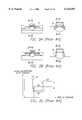
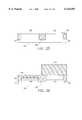
- the current method of producing a MOSFET on a polished silicon waferencompasses numerous individual steps which are often grouped into major process steps. These process steps commonly begin with an undoped silicon wafer 10, as shown in FIG. 1a, on which a pad oxide layer 11 and a nitride layer 13 are formed.
- isolationwherein the undoped silicon wafer 10 is divided by a number of isolation regions 12 (such as SiO 2 ) into separate areas in which individual devices are to be located, as shown in FIG. 1b.
- isolation regions 12such as SiO 2
- a sacrificial oxideis often suitably deposited above the active regions; followed by the implantantation of the deep well.
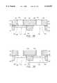
- Well implantationdetermines the electrical properties of the device (i.e., whether the transistor will be NMOS or PMOS). For example, an NMOS has a p-doped well 16 (identified by the "p") and a PMOS has an n-doped well 18 (identified by the "n”), as shown in FIG. 1c.
- the gate stackis commonly formed.
- a gate oxide 20is grown in the location where the channel will eventually be formed.
- a poly-silicon layer 22is then deposited on top of the gate oxide 20, as shown in FIG. 1d.
- the gate(the combination of the gate oxide 20 and the poly-silicon 22) is patterned, as shown in FIG. 1e.
- This stepbasically determines the length of the gate 22, and designates the level of technology (i.e., in the realm of semiconductor devices, the gate length is commonly used as a benchmark of the technology, wherein a smaller gate length indicates a more advanced technology).
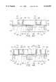
- Source and drain implantationcommonly occurs in two steps, the first of which is commonly referred to as the implantation of Lightly Doped Drains and Source (LDDS).
- LDDSLightly Doped Drains and Source
- lightly doped regions 25are created on either side of the gate, as shown in FIG. 1f.
- RTPRapid Thermal Processing
- spacers 26are formed on either side of the gate and then highly doped junction regions 27 are implanted using known techniques and dopants, as shown in FIG. 1g.
- the junctionsare then thermally annealed using known annealing processes.
- the last stepprovides for the formation of ohmic contacts through self-aligned silicidation.
- silicidationthe region above the source, drain, and the poly-silicon gate are covered with a low resistivity metallic silicide film 30, as shown in FIG. 1h.
- the spacers 26physically and electrically separate the gate 20/22 from the source and drain junctions 25/27.
- RTPRapid Thermal Processing
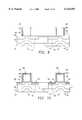
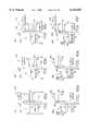
- FIG. 2ashows a shallow profile 32 and FIG. 2b shows the desired steep profile 34.
- FIG. 2cshows a relative graph (for illustrative purpose only, and not to reflect actual doping profiles) of the doping concentration versus the depth of the structure for a shallow profile (i.e., along the line A--A in FIG. 2a) and a deep profile (i.e., along the line BB in FIG. 2b). As shown in FIG.
- the shallow profile 32(“A--A”) has a lower doping concentration in the substrate closest to the gate oxide (i.e., the area of the graph indicated by "100") and a larger doping concentration deeper in the substrate (i.e., area "102").
- the steep profile 34(i.e., "B--B” or area "104") has a constant doping concentration throughout the substrate.
- the shallow profilei.e., "A--A”
- the steep profile 34is desired because it results in better charge carrier mobility and therefore a higher current drive capability.
- HCEHot Carrier Effect
- HCEHCE
- the operating voltage of the devicedecreases as the gate length decreases, in ⁇ 0.13 micron devices, the electric field generated does not accelerate the charge carriers to the point of thermal break through. Additionally, as the gate voltage of the device decreases, the series resistance of the source and drain regions becomes ever more important when compared to the resistance of the inversion layer.
- the new process flowencompasses many of the process steps of the prior art up to the point of isolation (that is, the present invention begins with an undoped wafer with a sacrificial oxide).
- the present inventionproceeds with deep well implantation, junction formation, silicidation, local self-aligned well implantation, channel growth, and the formation of the gate stack.
- the processing hurdles avoided by the present inventioninclude the concern over impurities entering the channel region during junction formation. Since the present invention preferably does not produce a channel until after the junctions have been formed, the channel region ultimately formed is not affected by impurities introduced by the junction profiles.
- Another hurdle the present invention avoids,is undesirable doping profiles in the channel caused by high temperatures. Since the method of the present invention does not produce the channel film until after all the ion implantations and the associated thermal annealing processes have been completed, the channel film is preferably not exposed to the high temperatures of the prior art methods. As a result, undoped materials may be used as the channel film, thereby improving the charge carrier mobility of the channel film.
- the present inventionalso allows gate insulators with large dielectric constants and metallic gate electrodes to be utilized.
- the present inventionavoids the hurdle present in the prior art method of exposing the gate stack to high temperatures and thus requiring the use of highly doped silicon as the gate electrodes.
- the entire gate stack of the present inventionavoids these high temperatures, because the gate stack is preferably not fabricated until after ion implantations have occurred.
- the channelcan be produced with silicon-based alloys.
- silicon-based alloyscommonly have narrower band-gaps which result in charge carriers with lower effective masses and higher mobility. As a result, this narrower band-gap allows lower threshold voltages without degrading the sub-threshold characteristics.
- the present inventionprovides a new process step for producing a gate stack in a MOSFET without encountering the obstacles and shortfalls of the prior art process flows.
- the new process step for producing the gate stackmay be suitably used with any process flow, e.g., the new process flow of the present invention or the process flow of the prior art.
- This new process steppreferably provides for the placement of a sacrificial gate structure in the location where the actual gate is to be formed. The sacrificial gate structure is then removed after all implantations have occurred, and the actual channel and gate materials are then deposited.
- FIG. 1is a schematic view of a cross-sectional representation of the formation of a semiconductor device using the process flow of the prior art.
- FIG. 2is a schematic view of a cross-sectional representation of the various junction shapes utilized in the formation of a semiconductor device under the process flow of the prior art.
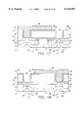
- FIG. 3is a schematic view of a cross-sectional representation of a non-doped silicon wafer into which an isolation region has been inserted and upon which an oxide and an amorphous silicon layer have been deposited under the process flow of the first embodiment of the present invention.
- FIG. 4is a schematic view of a cross-sectional representation of the wafer of FIG. 3 after the patterning of the amorphous silicon has occurred under the process flow of the first embodiment of the present invention.
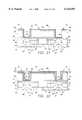
- FIG. 5is a schematic view of a cross-sectional representation of the wafer of FIG. 4 after the deep well and junctions for an NMOS have been implanted into the substrate under the process flow of the first embodiment of the present invention.
- FIG. 6is a schematic view of a cross-sectional representation of the wafer of FIG. 5 after the deep well and junctions for a PMOS have been implanted into the substrate under the process flow of the first embodiment of the present invention.
- FIG. 7is a schematic view of a cross-sectional representation of the wafer of FIG. 6 after the oxidation of the amorphous silicon sacrificial gate stacks has occurred under the process flow of the first embodiment of the present invention.
- FIG. 8is a schematic view of a cross-sectional representation of the wafer of FIG. 7 after the deposition and etchback of nitride spacers has occurred under the process flow of the first embodiment of the present invention.
- FIG. 9is a schematic view of a cross-sectional representation of the wafer of FIG. 8 after the cleaning and etching of the sacrificial oxide layer has occurred under the process flow of the first embodiment of the present invention.
- FIG. 10is a schematic view of a cross-sectional representation of the wafer of FIG. 9 after the formation of silicide has occurred under the process flow of the first embodiment of the present invention.
- FIG. 11is a schematic view of a cross-sectional representation of the wafer of FIG. 10 after the selective etching of the nitride spacers has occurred under the process flow of the first embodiment of the present invention.
- FIG. 12is a schematic view of a cross-sectional representation of the wafer of FIG. 11 after the selective etching of the oxide layers has occurred under the process flow of the first embodiment of the present invention.
- FIG. 14is a schematic view of a cross-sectional representation of the wafer of FIG. 13 after the planarization of the oxide and nitride layers has occurred under the process flow of the first embodiment of the present invention.
- FIG. 15is a schematic view of a cross-sectional representation of the wafer of FIG. 14 after nitrogenation has occurred under the process flow of the first embodiment of the present invention.
- FIG. 16is a schematic view of a cross-sectional representation of the wafer of FIG. 15 after selective etching of the sacrificial gate structure has occurred under the process flow of the first embodiment of the present invention.
- FIG. 17is a schematic view of a cross-sectional representation of the wafer of FIG. 16 after the implantation of a PMOS local well has occurred under the process flow of the first embodiment of the present invention.
- FIG. 18is a schematic view of a cross-sectional representation of the wafer of FIG. 17 after the implantation of an NMOS local well has occurred under the process flow of the first embodiment of the present invention.
- FIG. 19is a schematic view of a cross-sectional representation of the wafer of FIG. 18 after a pre-gate epitaxial cleaning of the device has occurred under the process flow of the first embodiment of the present invention.
- FIG. 20is a schematic view of a cross-sectional representation of the wafer of FIG. 19 after the deposition of the channel material has occurred under the process flow of the first embodiment of the present invention.
- FIG. 21is a schematic view of a cross-sectional representation of the wafer of FIG. 20 after the deposition of a gate insulator has occurred under the process flow of the first embodiment of the present invention.
- FIG. 22is a schematic view of a cross-sectional representation of the wafer of FIG. 21 after the deposition of a gate electrode has occurred under the process flow of the first embodiment of the present invention.
- FIG. 23is a schematic view of a cross-sectional representation of the wafer of FIG. 22 after the deposition of a second gate electrode has occurred under the process flow of the first embodiment of the present invention.
- FIG. 24is a schematic view of a cross-sectional representation of the wafer of FIG. 23 after planarization of the device structure has occurred under the process flow of the first embodiment of the present invention.
- FIG. 25is a schematic view of a cross-sectional representation of a non-doped silicon wafer into which isolation regions have been inserted and upon which an oxide layer has been deposited.
- FIG. 26is a schematic view of a cross-sectional representation of the wafer of FIG. 25 after implantation of an NMOS junction has occurred under the process flow of the second embodiment of the present invention.
- FIG. 27is a schematic view of a cross-sectional representation of the wafer of FIG. 26 after implantation of a PMOS junction has occurred under the process flow of the second embodiment of the present invention.
- FIG. 28is a schematic view of a cross-sectional representation of the wafer of FIG. 27 after etching of the sacrificial oxide has occurred under the process flow of the second embodiment of the present invention.
- FIG. 29is a schematic view of a cross-sectional representation of the wafer of FIG. 28 after deposition of a silicide has occurred under the process flow of the second embodiment of the present invention.
- FIG. 30is a schematic view of a cross-sectional representation of the wafer of FIG. 29 after the patterned selective etching of the silicide has occurred under the process flow of the second embodiment of the present invention.
- FIG. 31is a schematic view of a cross-sectional representation of the wafer of FIG. 30 after the deposition of a sacrificial oxide and a layer of amorphous silicon has occurred under the process flow of the second embodiment of the present invention.
- FIG. 32is a schematic view of a cross-sectional representation of the wafer of FIG. 31 after the patterning of the sacrificial gates has occurred under the process flow of the second embodiment of the present invention.
- FIG. 33is a schematic view of a cross-sectional representation of the wafer of FIG. 32 after the selective etching of the oxide has occurred under the process flow of the second embodiment of the present invention.
- FIG. 34is a schematic view of a cross-sectional representation of the wafer of FIG. 33 after the deposition of a nitride liner and an oxide has occurred under the process flow of the second embodiment of the present invention.
- FIG. 35is a schematic view of a cross-sectional representation of the wafer of FIG. 34 after planarization of the wafer has occurred under the process flow of the second embodiment of the present invention.
- FIG. 36is a schematic view of a cross-sectional representation of the wafer of FIG. 35 after the selective etching of the amorphous silicon has occurred under the process flow of the second embodiment of the present invention.
- FIG. 37is a schematic view of a cross-sectional representation of the wafer of FIG. 36 after the implantation of a PMOS well has occurred under the process flow of the second embodiment of the present invention.
- FIG. 38is a schematic view of a cross-sectional representation of the wafer of FIG. 37 after the implantation of an NMOS well has occurred under the process flow of the second embodiment of the present invention.
- FIG. 39is a schematic view of a cross-sectional representation of the wafer of FIG. 38 after the etching of the sacrificial oxide has occurred under the process flow of the second embodiment of the present invention.
- FIG. 40is a schematic view of a cross-sectional representation of the wafer of FIG. 39 after the selective growth of the channel material has occurred under the process flow of the second embodiment of the present invention.
- FIG. 41is a schematic view of a cross-sectional representation of the wafer of FIG. 40 after the deposition of a gate insulator and a gate electrode has occurred under the process flow of the second embodiment of the present invention.
- FIG. 42is a schematic view of a cross-sectional representation of the wafer of FIG. 41 after the deposition of a second gate electrode has occurred under the process flow of the second embodiment of the present invention.
- FIG. 43is a schematic view of a cross-sectional representation of the wafer of FIG. 42 after the planarization of the gate electrode has occurred under the process flow of the second embodiment of the present invention.
- FIG. 44is a schematic view of a cross-sectional representation of the wafer of FIG. 43 after the formation of contact holes has occurred under the process flow of the second embodiment of the present invention.
- FIG. 45is a series of band-gap diagrams which show the band-gap narrowing and reduced threshold gate voltages which can be realized for an n-channel device under either process flow of the present invention.
- FIG. 46is a series of band-gap diagrams which show the band-gap narrowing and reduced threshold gate voltages which can be realized for a p-channel device under either process flow of the present invention.
- the present inventionprovides a process flow for producing MOSFETs using standard, currently available MOSFET fabrication equipment and techniques. While the present invention is preferably directed towards the production of MOSFETs in the ⁇ 0.25 micron generation, it is to be appreciated that any size or generation of MOSFET devices may be produced using the methods described herein.
- the present inventionis discussed in the context of a first embodiment and a second embodiment. However, the present invention is not to be limited to the process flows described herein, any process flow or rearrangement of process steps which captures the features of the present invention is considered to be within the scope of the present invention. Additionally, the multiple embodiments of the present invention shall be described herein in conjunction with the formation of twin well structures. However, MOSFETs under process flows described herein may be formed as single well and/or multiple well NMOS and/or PMOS devices without departing from the spirit or scope of the present invention.
- the process flow for fabricating MOSFETspreferably includes the following steps:
- isolation zonesare inserted;
- a region of amorphous silicon and high energy implantsare used to create a deep well within the area under the layer of amorphous silicon resulting in a crest in the deep well layer below the area in which the gate will later be formed. Additionally, junctions are created on either side of the future channel region;
- Silicideis grown above the junctions and a sacrificial gate of amorphous silicon
- Nitride spacerare formed above the silicide regions
- a self-aligned local wellis implanted above the crest of the earlier deeply implanted well
- Channel material(preferably undoped film) is epitaxially deposited above the well;
- a gate insulator(preferably a material with a high dielectric) is in-situ deposited
- a gate electrode(preferably a barrier metal) is in-situ deposited
- a bulk gate electrode(preferably a highly conductive metal) is deposited.
- CMPChemical Mechanical Polishing
- the first steppreferably begins with the receipt of a non-doped wafer 10 into which an isolation 12 region has been inserted as shown in FIG. 3.
- the methods of inserting an isolation region into a non-doped silicon or similar (including germanium) waferis commonly known in the art and therefore is not discussed in detail herein. Any suitable isolation method may be utilized in the process flow of the present invention.
- Oxide layer 40 and an Amorphous Silicon (hereafter, " ⁇ -Si") layer 42is preferably deposited upon the non-doped wafer using methods commonly known in the art.
- Oxide layer 40is deposited upon the non-doped wafer 10 to a thickness in the range of 3 to 15 nanometers with a preferred thickness of 10 nanometers.
- the present inventionis not to be so limited and it is to be appreciated that the Oxide layer 40 may be of any thickness sufficient to provide any desired effects, including insulation, separation, and providing the base elements necessary for the growth or formation of various layers and/or structures which comprise a MOSFET.
- the second step of the first embodimentpreferably provides for the formation of sacrificial gates 46 above the region in which the actual gates are later to be formed.
- This stepuses standard process techniques for depositing compounds, patterning structures, and selectively etching the deposited compounds.
- ⁇ -Siis preferably used as the sacrificial compound.
- the ⁇ -Si layer 42is preferably deposited and etched such that sacrificial gates 46 are formed above the actual gate regions as shown in FIG. 4.
- the width of the photo resist mask 44 positioned above the ⁇ -Si layer 42will eventually determine the gate length. Therefore, the dimensions of the photo resist mask 44 are critical in providing a future region wherein the actual gate structure may be formed under the process flow of this embodiment of the present invention. Since the creation, formation, and positioning of photo resist masks is commonly known, they are not discussed further herein. After sacrificial gates 46 of the desired dimensions are suitably formed, the photo resist mask 44 is preferably removed and the structure is suitably cleaned.
- the third step of the process flow of the first embodiment of the present inventionpreferably provides for the implantation of the deep wells followed by the implantation of the junctions for a first device structure (an NMOS or a PMOS), and then the implantation of the deep wells and junctions for the opposite device structure (a PMOS or an NMOS, respectively).
- the deep wellsare self-aligned with the sources and drains using commonly known processes.
- a photo resist mask 48is suitably positioned above those regions of the non-doped wafer in which a PMOS structure is to be formed.
- the right side of the structureis to be a PMOS while the left side is an NMOS.
- either sidemay be suitably configured as a PMOS or an NMOS.
- a p-doped deep well 52is preferably formed by high energy ion implantation using known techniques. Since no other dopants have been implanted into the device structure at this point in the process flow, the well may be suitably driven in and formed without concern for the contamination of other structures.
- n+ doped source and drain junctions 50are implanted using known techniques.
- the photo resist maskis suitably repositioned over the NMOS region, as shown in FIG. 6, and a PMOS device is formed by using known implantation techniques, resulting in an n-doped deep well 53 and p+ doped junctions 51.
- the process flow of the present inventionis preferably to be utilized for devices with a very low operating voltage, HCE is not a concern.
- the junctionsmay be steep instead of shallow and may be suitably implanted in one process step.
- the present inventioneliminates the need to first form a shallow junction followed by a deeper junction, and thus simplifies the process flow for junction formation.
- the present inventionis not to be construed as being limited to producing only ⁇ 0.25 micron generation devices wherein steep junctions are preferred. In fact any form or size of junctions, whether shallow or steep, may be suitably formed using known methods without departing from the spirit or scope of the present invention.
- the deviceis preferably subjected to Rapid Thermal Processing (RTP), or similar processing techniques, to anneal the implants.
- RTPRapid Thermal Processing
- the process flow of the present inventioneliminates many of the thermal budget constraints of the prior methods, and allows for the junctions to be firmly set and full annealing accomplished.
- the process flow of the present inventionalso permits thermal processing to be postponed until later in the process flow. The thermal annealing can be delayed until after the local well has been implanted, but before the gate stack has been formed, without reducing any of the advantages of the process flow or departing from the spirit or the scope of the present invention.
- the fourth steppreferably provides the process steps necessary for the eventual formation of a self-aligned silicide on the source and drain junctions 50 and 51.
- These process stepspreferably include: (1) the formation of an oxidation layer 54 upon the sacrificial gates 46 (as shown in FIG. 7); (2) the Chemical Vapor Deposition (CVD) of nitride Si 3 N 4 56 upon the oxide layer 54 (as shown in FIG. 8); and (3) the etchback of the nitride 56, oxide 54, and the sacrificial oxide 40 (as is shown in FIG. 9).
- nitride region 56is preferably formed so as to provide an electrical isolation layer between any silicide deposited on top of the sacrificial gate 46 and the junctions 50 and 51.
- the fifth steppreferably provides for the formation of self-aligned suicides 58 in the junctions 50 and 51 and/or in the sacrificial gate 46 using known techniques (as shown in FIG. 10).
- the sixth step of this embodiment of the present inventionpreferably provides those process steps necessary to prepare the device for the formation of the self-aligned wells. These process steps preferably include: (1) selective etching of the nitride 56 against the oxide 54 and silicide 58 (as shown in FIG. 11); (2) selective etching of the oxide 54 against the sacrificial gate 46 and the silicide 58 (as shown in FIG. 12); (3) CVD of a nitride liner 60 and an oxide 62 trench fill (as shown in FIG. 13); (4) planarization and CMP of oxide and nitride 60 stopping on the sacrificial gate 46 (as shown in FIG.
- the seventh step of this embodiment of the present inventionpreferably provides for the photo resist masking off of those regions within which an alternative device structure is to be formed.
- the region within which an NMOS is to be formedis masked off while the PMOS region is exposed to ion implantations which preferably form a self-aligned n-doped local well 69.
- the region within which a PMOS is to be formedis masked off while the NMOS region is exposed to ion implantations which preferably form a self-aligned p-doped local well 68.
- NMOS regionmay be formed prior to the formation of the other region.
- NMOS or PMOS regionmay be separately formed regardless of whether a counterpart PMOS or NMOS region is formed.
- the gate regions 59are cleaned and the oxide layer 40 in the gate regions 59 is suitably removed (as shown in FIG. 19).
- the deviceis then preferably baked at a sufficient temperature to ensure the structures formed up to this point are fixed in the wafer structure.
- RTP or similar device baking techniques known in the artmay be utilized to ensure the well and junction regions are electrically activated and any defects are annealed. Additionally, these baking processes are preferably performed using known techniques to ensure the surface is suitable for epitaxial deposition of the channel film.
- the eighth step of this embodiment of the present inventionpreferably provides for the deposition of the channel material 70 (as shown in FIG. 20).
- the depositionis performed epitaxially and is selectively applied; the channel material selected is an undoped film which provides for maximum electron and hole mobility.
- the channel materialmay preferably be a silicon based alloy with a narrower band-gap and lower effective masses (electron and hole).
- the present inventionis not to be construed as being limited to only silicon based alloys, any material which can be deposited pseudo-morphically on silicon is considered to be within the scope of the present invention.
- the ninth step of this embodiment of the present inventionpreferably provides for the formation of the gate stack.
- the formation of the gate stackpreferably begins with the in-situ deposition of a gate insulator 72 above the channel 70 (as shown in FIG. 21).
- the gate insulatoris such that a very large capacitance is obtained.
- Metal oxidesincluding compounds such as Ta 2 O 5 or TiO 2 (both of which may be suitably deposited via CVD), which preferably provide a larger capacitance than silicon dioxide (SiO 2 ), may be utilized in the present invention as the gate insulator because the process of the present invention generally does not expose the gate insulator to high temperatures.
- the present inventionis not limited to the use of a metallic oxide as the gate insulator, any compound (including silicon dioxides, silicon nitrides, or the like) which provides the desired capacitance and insulation (both physical and electrical) may be utilized.
- the formation of the gate stackpreferably continues with the in-situ deposition of the gate electrode.
- the deposition of the gate electrodemay constitute multiple layers wherein more conductive metals are subsequently deposited upon previously deposited layers.
- the conductivity of the gate electrode material chosen, and the electrical insulation desiredin part a determination of the power levels utilized, and other factors known in the art
- any number of gate electrode layersmay be utilized without departing from the spirit or scope of the present invention.
- a two layer gate electrodeis preferably utilized.
- a first layer 74 of the gate electrodemay preferably be a barrier metal such as TiN or TaSiN which may be suitably deposited upon the gate insulator by CVD.
- the gate electrode depositionis then preferably followed by the deposition of a second layer gate electrode 76 (as shown in FIG. 23).
- the second layer gate electrode 76may be any material which provides the desired electrical conductivity including poly-silicon compounds.
- the gate electrode 76is composed of a highly conductive metal such as tungsten, copper, or the like.
- the final process step of this embodiment of the present inventionprovides for planarization and thinning the device structure until the nitride layer 66 is reached (as shown in FIG. 24).
- the planarization and thinning of the deviceis accomplished via CMP, however, any method of planarizing and reducing the device structure is within the scope of the present invention.
- This final steppreferably removes the excess gate stack layers previously deposited on the device during the formation of the gate stack. At this point the device is ready for back-end processing using existing and known techniques.
- MOSFET with a short active areaincluding contacts to the source and the drain made over the isolation regions. Additionally, this embodiment preferably retains the several features and characteristics of the new process flow, namely the formation of the channel and gate stack after the wells and junctions have been formed. As a general overview, the second embodiment of the present invention preferably includes the following process steps:
- isolation zonesare inserted;
- a junctionis implanted between the isolation zones
- the silicideis selectively etched
- a sacrificial oxide layer and an amorphous silicon layerare deposited
- Gatesare patterned by selectively etching a layer of amorphous silicon previously deposited above the sacrificial oxide layer;
- the oxide layeris selectively etched except for those areas under the amorphous silicon layer (i.e., the region where the gate stack will be formed);
- a nitride layeris deposited upon the surface areas followed by an oxide layer to fill in any trenches;
- CMPis applied to the oxide layer until the top region of the amorphous silicon is reached at which time the amorphous silicon is selectively etched;
- a self-aligned wellis then implanted through the region from which the amorphous silicon was previously removed;
- the sacrificial oxide above the gate regionis removed and the channel material (preferably an undoped film) is epitaxially grown;
- a gate insulator and gate electrodeare deposited on the surface
- a bulk metal gate electrodeis deposited on all surface areas
- CMPis applied to the structure and all layers are removed until the oxide layer is reached.
- the first step of this second embodimentpreferably begins with a non-doped wafer 100 within which isolation zones 102 have been formed such that short "active" areas 104 and 105 arise, as shown in FIG. 25. Additionally, an oxide layer 106 has been deposited upon the non-doped wafer 100 using methods commonly known in the art. Oxide layer 106 is preferably deposited upon the non-doped wafer 100 to a thickness in the range of three to fifteen nanometers with a preferred thickness of ten nanometers. However, the present invention is not to be limited and it is to be appreciated that the oxide layer 106 may be of any thickness sufficient to provide the desired effects, including insulation, separation, and providing the base elements necessary for the growth or formation of various layers and/or structures.
- the second step of the process flow of the second embodiment of the present inventionpreferably provides for the implantation of the junctions.
- NMOS junctionsare implanted before PMOS junctions.
- the present inventionis not to be so limited, either NMOS or PMOS junctions may be formed first without departing from the spirit or scope of the present invention.
- this embodiment of the present inventionis disclosed in the context of the formation of a twin well transistor, it is to be understood that the present invention is not so limited, any active area 104 or 105 may be suitably configured to support the formation of an NMOS or a PMOS without departing from the spirit or scope of the present invention.
- a standard process mask 110is suitably positioned above those regions of the non-doped wafer 100 within which a PMOS is to be formed. N++ ions are then implanted into the short active area 104, using known techniques, and an n++ junction 108 is formed, as shown in FIG. 26.
- a standard process mask 110is suitably positioned above those regions within which the NMOS junctions were previously formed, as shown in FIG. 27.
- P++ ionsare then implanted into the short active area 105, using known techniques, and a p++ junction 109 is suitably formed.
- the process flow of the second embodiment of the present inventionmay also be optionally configured such that a deep well is implanted below each junction.
- deep well implantationoccurs at a later stage in the process.
- the third step of the second embodimentprovides for the etching of the sacrificial oxide 106 and the pre-epitaxial baking of the structures formed up to this point, as shown in FIG. 28.
- the pre-epitaxial baking steppreferably anneals the implanted junctions, thus any known baking process may be utilized which provides the time-temperature gradients needed to anneal the junction implants.
- the preferred process flow for this second embodiment of the present inventionprovides for a pre-epitaxial baking at this point in the process flow, it is to be understood that the baking and thereby the annealing of the junctions may occur at any time in the process flow prior to the growth of the channel material without departing from the spirit or scope of the present invention.
- the present inventionpreferably provides for the annealing of any junction implantation defects, and allows inspection and verification of acceptable junction formation early in the process flow.
- the fourth step of this embodimentpreferably provides for the formation (preferably via CVD) of an epitaxial layer of a compatible conductive layer 112 (for example, TiSi 2 or TiN), as shown in FIG. 29.
- a compatible conductive layer 112for example, TiSi 2 or TiN
- the CVD of a silicideis preferably performed using known techniques.
- a photo-resist mask 114is suitably positioned above those regions in which the conductive layer 112 is to remain.
- the remaining silicidei.e., the silicide not under the mask 1114 is suitably etched.
- Local interconnectsare then preferably patterned and any remaining conductive layer 112 is suitably removed from the gate region, as shown in FIG. 30.
- the etching of the silicide and patterning of the local interconnectsis suitably accomplished via known techniques.
- the sixth step of this embodimentmay include a number of process steps for forming a sacrificial gate stack which is electrically isolated from the junction regions. While the present invention is described as encompassing a specific series of process steps, any combination of process steps which provide for the formation of an electrically isolated gate region while providing the desired structure above the junctions is considered to be within the scope of the present invention.
- these process stepsinclude: (1) depositing (preferably via CVD) a suitably thin sacrificial oxide 116 (preferably SiO 2 ,), as shown in FIG.
- a poly-silicon layer 118such as Amorphous Silicon or " ⁇ -Si"
- ⁇ -SiAmorphous Silicon
- ⁇ -SiAmorphous Silicon
- FIG. 32suitably positioning a photo resist mask upon the device structure and selectively etching the poly-silicon layer 118 such that sacrificial gates 119 are formed, as shown in FIG. 32; (4) selectively etching the sacrificial oxide 116 against the conductive layer 112, junctions 108 and 109, and the sacrificial gates 119, as shown in FIG. 33; (5) depositing a dielectric insulator 120 (preferably SiN), as shown in FIG.
- a dielectric insulator 120preferably SiN
- the selective etching of the poly-silicon layer 118 which results in the sacrificial gates 119is preferably the process step at which the particular gate length (and the generation of technology) is suitably determined.
- the particular gate lengthand the generation of technology
- the seventh step of the second embodiment of the present inventionpreferably provides for the selective etching of the sacrificial gate 119, as shown in FIG. 36.
- a mask 124is suitably positioned such that a PMOS self-aligned local well 126 may be implanted, using known well implantation techniques, as shown in FIG. 37.
- the mask 124is suitably removed and the structure cleaned via known techniques.
- a mask 130is then suitably positioned to provide the patterning necessary for the implantation of an NMOS self-aligned local well 138, using known techniques, as shown in FIG. 38.
- the NMOS and PMOS self-aligned wellsare formed such that shallow junctions do not arise.
- the process flow of the present inventionmay be suitably modified to form shallow junctions when desired, by suitably modifying the ionization energy, pattern, duration, and/or intensity of the dopants utilized in forming the junctions and the wells.
- the eighth step of the second embodiment of the present inventionpreferably provides for the removal of the sacrificial oxide 116 followed by the baking of the structure. Any suitable method of baking the structure may be utilized to electrically activate the well and anneal impurities in the well and/or junctions. The resulting structure is shown in FIG. 39.
- the present inventionprovides for the formation of the junctions and wells and subjects the structure to high thermal processing prior to the formation of the channel and the gate.
- the ninth stepprovides for the low temperature epitaxial growth of the channel 132, as shown in FIG. 40.
- the channel 132is an undoped film which provides for maximum electron and hole mobility.
- the channel 132 materialmay preferably be a silicon based alloy with a narrower band-gap and lower effective electron and hole masses.
- the present inventionis not to be construed as being limited to silicon based alloys; any material which can be suitably deposited on silicon (and preferably, pseudo-morphically deposited on silicon) is considered to be within the scope of the present invention.
- the channel 132 materialis preferably a SiGeC film.
- the gate stackis preferably formed.
- the formation of the gate stackis a multi-step process.
- the first step of this processpreferably is the deposition (preferably via CVD) of the gate insulator 134, as shown in FIG. 41.
- the gate insulator 134is selected such that a very large capacitance is obtained.
- the present inventionallows metal oxides to be used as the gate insulator 134 because the process flow of the present invention does not expose the gate insulator 134 to the high temperatures commonly used to anneal implants.
- the present inventionis not limited to the use of a metallic oxide as the gate insulator 134, any compound including silicon dioxides, silicon nitrides, or the like which provide the desired physical characteristics may be utilized.
- the formation of the gate stackpreferably continues with the in-situ deposition of the gate electrode.
- the deposition of the gate electrodemay constitute a multiple layer approach wherein more conductive metals are subsequently deposited upon previously deposited layers.
- the conductivity of the gate electrode, and the electrical insulation neededvarious layers of gate electrodes may be used. However, in this embodiment of the present invention, a two layer gate electrode is preferably utilized.
- a first layer 136 of the gate electrodemay be a barrier metal such as TiN or TaSiN which may be suitably deposited (preferably via CVD) upon the gate insulator 134.
- the second layer 138 of the gate electrodemay be any material which provides the desired electrical conductivity, including poly-silicon compounds.
- the gate electrodeis composed of highly conductive metal such as tungsten, copper, or the like.
- planarizationis performed until the oxide layer 122 is reached.
- Planarizationmay be performed via any method known in the art, and preferably via CMP.
- contacts openings 140 over the source and drain junction fieldsmay be suitably etched.
- the deviceis ready for subsequent processing (including metallization also known as back-end processing) using known in the art techniques.
- the process flows of the present inventionalso significantly reduce the concern of impurities arising in the channel region (i.e., where the transport of electrons and holes takes place). Since the junctions are preferably implanted before the local well is formed, impurities which arise in the well region can be suitable annealed or similarly reduced and/or eliminated using known techniques. Thus, the present invention preferably provides a channel region in which a low concentration (if any) of impurities exist and a high mobility of electrons and holes can arise.
- Another advantage of the process flows of the present inventionis that it allows silicon-based alloys to be used as the channel material.
- Silicon-based alloyscommonly have narrower band-gaps and charge carriers (i.e., electrons and holes) with lower effective masses, higher mobility, and a lower density of states.
- materials with narrower band-gaps and charge carriers with lower effective massesrequire less threshold voltage to be excited.
- the process flows of the present inventionallow a reduction to occur in the threshold voltage necessary to operate the MOSFET.
- a device 240 produced under the standard process flow with a p-type silicon substrate 204, a gate insulator 200, and an n+ poly-silicon gate electrode 202commonly has band-gap with a relatively steep profile, as shown in the band-gap energy diagram in FIG. 45a.
- FIG. 45dshows the device of FIG. 45a when a threshold gate voltage V G1 is applied to the n+ poly-silicon gate electrode 202.
- a band-gap energy diagram for a semiconductor devicegenerally shows the increased energy at the gate electrode (which translates into the threshold voltage) necessary to excite through the gate insulator 200 the electrons in the substrate 204 from the valence band (E v ) to the conduction band (E c ); wherein E F is the Fermi level (i.e., the energy at which the probability of an electron occupying either the conduction band or the valence band is fifty percent), and E i is the Fermi level of an intrinsic semiconductor (i.e. an ideal device which has few impurities).
- the n+ poly-silicon gate electrode 202 in device 240is replaced by a gate electrode with a mid-gap work function 206, as shown in FIG. 45b, the bending 212 in the channel formed in the substrate 204 is reduced and the surface potential for device 250 is higher than the surface potential for device 240 (i.e. E C is below E F for device 240, and E C is above E F for device 250) and a higher threshold voltage occurs, as shown in FIG. 45e by the higher threshold gate voltage V G2 necessary to reach the Fermi level, E F (i.e., V G2 is greater than V G1 ).
- the present inventionallows a channel 208 with a band-gap narrower than silicon to be utilized.
- the channel 208lowers the surface potential on the semiconductor such that a lower threshold gate voltage V G3 may be utilized to activate the device 260 (i.e., V G3 is approximately equal to V G1 and V G3 is less than V G2 ).
- FIGS. 46a-fdepict the band diagrams for an n-type silicon substrate, and reflects the gate voltages, band bending, and the like which occurs when a p-channel device is produced.
- the advantages of the present inventionare also realized in a PFET by using a mid-gap workfunction gate electrode and a channel having a band-gap narrower than silicon.
- a deviceis produced in which the same surface potential exists at both the gate oxide and the channel.
- Such an ideal devicewould have a metal gate electrode with a mid-gap workfunction while providing a low threshold gate voltage.
- Such an ideal devicecould be produced using, for example, Si 1-x Ge x and Si 1-y C y films as the channel material.
Landscapes
- Engineering & Computer Science (AREA)
- Computer Hardware Design (AREA)
- Power Engineering (AREA)
- Microelectronics & Electronic Packaging (AREA)
- Physics & Mathematics (AREA)
- Manufacturing & Machinery (AREA)
- Condensed Matter Physics & Semiconductors (AREA)
- General Physics & Mathematics (AREA)
- Chemical Kinetics & Catalysis (AREA)
- Chemical & Material Sciences (AREA)
- General Chemical & Material Sciences (AREA)
- Crystallography & Structural Chemistry (AREA)
- Insulated Gate Type Field-Effect Transistor (AREA)
- Electrodes Of Semiconductors (AREA)
- Metal-Oxide And Bipolar Metal-Oxide Semiconductor Integrated Circuits (AREA)
Abstract
Description
Claims (15)
Priority Applications (5)
| Application Number | Priority Date | Filing Date | Title |
|---|---|---|---|
| US09/162,272US6143593A (en) | 1998-09-29 | 1998-09-29 | Elevated channel MOSFET |
| PCT/US1999/019526WO2000019510A2 (en) | 1998-09-29 | 1999-08-26 | Elevated channel mosfet |
| EP99969844AEP1121716A2 (en) | 1998-09-29 | 1999-08-26 | Elevated channel mosfet |
| JP11274038AJP2000138183A (en) | 1998-09-29 | 1999-09-28 | A method of protecting a metal from oxidation during formation of a poly metal gate in semiconductor device manufacturing. |
| US09/616,233US6630710B1 (en) | 1998-09-29 | 2000-07-14 | Elevated channel MOSFET |
Applications Claiming Priority (1)
| Application Number | Priority Date | Filing Date | Title |
|---|---|---|---|
| US09/162,272US6143593A (en) | 1998-09-29 | 1998-09-29 | Elevated channel MOSFET |
Related Child Applications (1)
| Application Number | Title | Priority Date | Filing Date |
|---|---|---|---|
| US09/616,233DivisionUS6630710B1 (en) | 1998-09-29 | 2000-07-14 | Elevated channel MOSFET |
Publications (1)
| Publication Number | Publication Date |
|---|---|
| US6143593Atrue US6143593A (en) | 2000-11-07 |
Family
ID=22584926
Family Applications (2)
| Application Number | Title | Priority Date | Filing Date |
|---|---|---|---|
| US09/162,272Expired - LifetimeUS6143593A (en) | 1998-09-29 | 1998-09-29 | Elevated channel MOSFET |
| US09/616,233Expired - Fee RelatedUS6630710B1 (en) | 1998-09-29 | 2000-07-14 | Elevated channel MOSFET |
Family Applications After (1)
| Application Number | Title | Priority Date | Filing Date |
|---|---|---|---|
| US09/616,233Expired - Fee RelatedUS6630710B1 (en) | 1998-09-29 | 2000-07-14 | Elevated channel MOSFET |
Country Status (4)
| Country | Link |
|---|---|
| US (2) | US6143593A (en) |
| EP (1) | EP1121716A2 (en) |
| JP (1) | JP2000138183A (en) |
| WO (1) | WO2000019510A2 (en) |
Cited By (25)
| Publication number | Priority date | Publication date | Assignee | Title |
|---|---|---|---|---|
| US6218254B1 (en)* | 1999-09-22 | 2001-04-17 | Cree Research, Inc. | Method of fabricating a self-aligned bipolar junction transistor in silicon carbide and resulting devices |
| US6329675B2 (en) | 1999-08-06 | 2001-12-11 | Cree, Inc. | Self-aligned bipolar junction silicon carbide transistors |
| US6335251B2 (en) | 1998-05-29 | 2002-01-01 | Kabushiki Kaisha Toshiba | Semiconductor apparatus having elevated source and drain structure and manufacturing method therefor |
| US20020195709A1 (en)* | 1996-06-03 | 2002-12-26 | Micron Technology, Inc. | Method for forming a metallization layer |
| US20030010308A1 (en)* | 2001-07-13 | 2003-01-16 | Unisia Jecs Corporation | Control apparatus and control method of negative pressure actuator |
| US6509586B2 (en)* | 2000-03-31 | 2003-01-21 | Fujitsu Limited | Semiconductor device, method for fabricating the semiconductor device and semiconductor integrated circuit |
| US6563178B2 (en)* | 2000-03-29 | 2003-05-13 | Matsushita Electric Industrial Co., Ltd. | Semiconductor device and method for fabricating the device |
| US6607950B2 (en)* | 2000-03-30 | 2003-08-19 | Interuniversitair Microelektronic Centrum (Imec) | MIS transistors with a metal gate and high-k dielectric and method of forming |
| US20030162335A1 (en)* | 1999-01-14 | 2003-08-28 | Matsushita Electric Industrial Co., Ltd. | Semiconductor device and method for fabricating the same |
| US20030207543A1 (en)* | 2002-01-14 | 2003-11-06 | Salling Craig T. | Structure and method of MOS transistor having increased substrate resistance |
| US20040007170A1 (en)* | 2002-07-09 | 2004-01-15 | Chartered Semiconductor Manufacturing Ltd. | Method of fabricating a CMOS device with integrated super-steep retrograde twin wells using double selective epitaxial growth |
| US20040026743A1 (en)* | 2000-11-16 | 2004-02-12 | Akihide Shibata | Semiconductor device and portable electronic apparatus |
| US6762469B2 (en) | 2002-04-19 | 2004-07-13 | International Business Machines Corporation | High performance CMOS device structure with mid-gap metal gate |
| US6806147B1 (en)* | 1999-11-22 | 2004-10-19 | Advanced Micro Devices, Inc. | Method and apparatus for suppressing the channeling effect in high energy deep well implantation |
| US20060154428A1 (en)* | 2005-01-12 | 2006-07-13 | International Business Machines Corporation | Increasing doping of well compensating dopant region according to increasing gate length |
| US20060226464A1 (en)* | 2005-03-30 | 2006-10-12 | Broadcom Corporation | High voltage gain topology for analog circuits in short channel technologies |
| US20060255412A1 (en)* | 2005-05-13 | 2006-11-16 | Nirmal Ramaswamy | Enhanced access devices using selective epitaxial silicon over the channel region during the formation of a semiconductor device and systems including same |
| US20070059929A1 (en)* | 2004-06-25 | 2007-03-15 | Hag-Ju Cho | Method of forming a tantalum carbon nitride layer and method of manufacturing a semiconductor device using the same |
| US20070155142A1 (en)* | 2005-12-30 | 2007-07-05 | Been-Yih Jin | Abrupt junction formation by atomic layer epitaxy of in situ delta doped dopant diffusion barriers |
| DE102010001404A1 (en)* | 2010-01-29 | 2011-08-04 | GLOBALFOUNDRIES Dresden Module One Limited Liability Company & Co. KG, 01109 | Adjustment of transistor properties based on a late well implant |
| US20140220755A1 (en)* | 2001-09-21 | 2014-08-07 | Taiwan Semiconductor Manufacturing Company, Ltd. | Semiconductor Structures Employing Strained Material Layers with Defined Impurity Gradients and Methods for Fabricating Same |
| US20150187898A1 (en)* | 2013-12-26 | 2015-07-02 | Semiconductor Energy Laboratory Co., Ltd. | Semiconductor device and method for manufacturing the same |
| US20170221796A1 (en)* | 2016-01-29 | 2017-08-03 | United Microelectronics Corp. | Through-silicon via structure |
| US20210217867A1 (en)* | 2020-01-10 | 2021-07-15 | Xia Tai Xin Semiconductor (Qing Dao) Ltd. | Semiconductor device and method for fabricating the same |
| US11217703B2 (en)* | 2015-04-13 | 2022-01-04 | Semiconductor Energy Laboratory Co., Ltd. | Semiconductor device and manufacturing method of the same |
Families Citing this family (83)
| Publication number | Priority date | Publication date | Assignee | Title |
|---|---|---|---|---|
| JP3264264B2 (en)* | 1999-03-01 | 2002-03-11 | 日本電気株式会社 | Complementary integrated circuit and manufacturing method thereof |
| GB2358737A (en)* | 1999-03-01 | 2001-08-01 | Nec Corp | Methods for manufacturing a complimentary integrated circuit |
| US6903411B1 (en)* | 2000-08-25 | 2005-06-07 | Agere Systems Inc. | Architecture for circuit connection of a vertical transistor |
| JP3634320B2 (en)* | 2002-03-29 | 2005-03-30 | 株式会社東芝 | Semiconductor device and manufacturing method of semiconductor device |
| US7122454B2 (en)* | 2002-06-12 | 2006-10-17 | Applied Materials, Inc. | Method for improving nitrogen profile in plasma nitrided gate dielectric layers |
| JP2004111611A (en) | 2002-09-18 | 2004-04-08 | Renesas Technology Corp | Semiconductor device and method of manufacturing the same |
| US7075150B2 (en)* | 2003-12-02 | 2006-07-11 | International Business Machines Corporation | Ultra-thin Si channel MOSFET using a self-aligned oxygen implant and damascene technique |
| TWI231960B (en)* | 2004-05-31 | 2005-05-01 | Mosel Vitelic Inc | Method of forming films in the trench |
| US7078722B2 (en)* | 2004-09-20 | 2006-07-18 | International Business Machines Corporation | NFET and PFET devices and methods of fabricating same |
| US7547605B2 (en)* | 2004-11-22 | 2009-06-16 | Taiwan Semiconductor Manufacturing Company | Microelectronic device and a method for its manufacture |
| US20060166417A1 (en) | 2005-01-27 | 2006-07-27 | International Business Machines Corporation | Transistor having high mobility channel and methods |
| US20080121932A1 (en) | 2006-09-18 | 2008-05-29 | Pushkar Ranade | Active regions with compatible dielectric layers |
| CN100505268C (en)* | 2005-03-21 | 2009-06-24 | 旺宏电子股份有限公司 | Memory device and method for accessing memory unit |
| US20060292762A1 (en)* | 2005-06-22 | 2006-12-28 | Epion Corporation | Replacement gate field effect transistor with germanium or SiGe channel and manufacturing method for same using gas-cluster ion irradiation |
| KR100673902B1 (en)* | 2005-06-30 | 2007-01-25 | 주식회사 하이닉스반도체 | Tungsten Polymetal Gate and Manufacturing Method Thereof |
| KR100703984B1 (en)* | 2006-03-22 | 2007-04-09 | 삼성전자주식회사 | Method for manufacturing semiconductor integrated circuit device and its structure |
| US7704844B2 (en)* | 2007-10-04 | 2010-04-27 | International Business Machines Corporation | High performance MOSFET |
| US7964487B2 (en)* | 2008-06-04 | 2011-06-21 | International Business Machines Corporation | Carrier mobility enhanced channel devices and method of manufacture |
| US20100330309A1 (en) | 2009-06-30 | 2010-12-30 | Guardian Industries Corp. | Frit or solder glass compound including beads, and assemblies incorporating the same |
| US8273617B2 (en) | 2009-09-30 | 2012-09-25 | Suvolta, Inc. | Electronic devices and systems, and methods for making and using the same |
| US8421162B2 (en) | 2009-09-30 | 2013-04-16 | Suvolta, Inc. | Advanced transistors with punch through suppression |
| US8530286B2 (en) | 2010-04-12 | 2013-09-10 | Suvolta, Inc. | Low power semiconductor transistor structure and method of fabrication thereof |
| US8569128B2 (en) | 2010-06-21 | 2013-10-29 | Suvolta, Inc. | Semiconductor structure and method of fabrication thereof with mixed metal types |
| US8759872B2 (en) | 2010-06-22 | 2014-06-24 | Suvolta, Inc. | Transistor with threshold voltage set notch and method of fabrication thereof |
| US9029834B2 (en) | 2010-07-06 | 2015-05-12 | International Business Machines Corporation | Process for forming a surrounding gate for a nanowire using a sacrificial patternable dielectric |
| US8377783B2 (en) | 2010-09-30 | 2013-02-19 | Suvolta, Inc. | Method for reducing punch-through in a transistor device |
| US8404551B2 (en) | 2010-12-03 | 2013-03-26 | Suvolta, Inc. | Source/drain extension control for advanced transistors |
| US8461875B1 (en) | 2011-02-18 | 2013-06-11 | Suvolta, Inc. | Digital circuits having improved transistors, and methods therefor |
| US8525271B2 (en) | 2011-03-03 | 2013-09-03 | Suvolta, Inc. | Semiconductor structure with improved channel stack and method for fabrication thereof |
| US8400219B2 (en) | 2011-03-24 | 2013-03-19 | Suvolta, Inc. | Analog circuits having improved transistors, and methods therefor |
| US8748270B1 (en) | 2011-03-30 | 2014-06-10 | Suvolta, Inc. | Process for manufacturing an improved analog transistor |
| US8999861B1 (en) | 2011-05-11 | 2015-04-07 | Suvolta, Inc. | Semiconductor structure with substitutional boron and method for fabrication thereof |
| US8796048B1 (en) | 2011-05-11 | 2014-08-05 | Suvolta, Inc. | Monitoring and measurement of thin film layers |
| US8811068B1 (en) | 2011-05-13 | 2014-08-19 | Suvolta, Inc. | Integrated circuit devices and methods |
| US8569156B1 (en) | 2011-05-16 | 2013-10-29 | Suvolta, Inc. | Reducing or eliminating pre-amorphization in transistor manufacture |
| US8735987B1 (en) | 2011-06-06 | 2014-05-27 | Suvolta, Inc. | CMOS gate stack structures and processes |
| US8995204B2 (en) | 2011-06-23 | 2015-03-31 | Suvolta, Inc. | Circuit devices and methods having adjustable transistor body bias |
| US8629016B1 (en) | 2011-07-26 | 2014-01-14 | Suvolta, Inc. | Multiple transistor types formed in a common epitaxial layer by differential out-diffusion from a doped underlayer |
| US8748986B1 (en) | 2011-08-05 | 2014-06-10 | Suvolta, Inc. | Electronic device with controlled threshold voltage |
| KR101891373B1 (en) | 2011-08-05 | 2018-08-24 | 엠아이이 후지쯔 세미컨덕터 리미티드 | Semiconductor devices having fin structures and fabrication methods thereof |
| US8994123B2 (en) | 2011-08-22 | 2015-03-31 | Gold Standard Simulations Ltd. | Variation resistant metal-oxide-semiconductor field effect transistor (MOSFET) |
| US8645878B1 (en) | 2011-08-23 | 2014-02-04 | Suvolta, Inc. | Porting a circuit design from a first semiconductor process to a second semiconductor process |
| US8614128B1 (en) | 2011-08-23 | 2013-12-24 | Suvolta, Inc. | CMOS structures and processes based on selective thinning |
| US8713511B1 (en) | 2011-09-16 | 2014-04-29 | Suvolta, Inc. | Tools and methods for yield-aware semiconductor manufacturing process target generation |
| US9236466B1 (en) | 2011-10-07 | 2016-01-12 | Mie Fujitsu Semiconductor Limited | Analog circuits having improved insulated gate transistors, and methods therefor |
| US8895327B1 (en) | 2011-12-09 | 2014-11-25 | Suvolta, Inc. | Tipless transistors, short-tip transistors, and methods and circuits therefor |
| US8819603B1 (en) | 2011-12-15 | 2014-08-26 | Suvolta, Inc. | Memory circuits and methods of making and designing the same |
| US8883600B1 (en) | 2011-12-22 | 2014-11-11 | Suvolta, Inc. | Transistor having reduced junction leakage and methods of forming thereof |
| US8599623B1 (en) | 2011-12-23 | 2013-12-03 | Suvolta, Inc. | Circuits and methods for measuring circuit elements in an integrated circuit device |
| US8970289B1 (en) | 2012-01-23 | 2015-03-03 | Suvolta, Inc. | Circuits and devices for generating bi-directional body bias voltages, and methods therefor |
| US8877619B1 (en) | 2012-01-23 | 2014-11-04 | Suvolta, Inc. | Process for manufacture of integrated circuits with different channel doping transistor architectures and devices therefrom |
| US9093550B1 (en) | 2012-01-31 | 2015-07-28 | Mie Fujitsu Semiconductor Limited | Integrated circuits having a plurality of high-K metal gate FETs with various combinations of channel foundation structure and gate stack structure and methods of making same |
| US9406567B1 (en) | 2012-02-28 | 2016-08-02 | Mie Fujitsu Semiconductor Limited | Method for fabricating multiple transistor devices on a substrate with varying threshold voltages |
| US9373684B2 (en)* | 2012-03-20 | 2016-06-21 | Semiwise Limited | Method of manufacturing variation resistant metal-oxide-semiconductor field effect transistor (MOSFET) |
| US8863064B1 (en) | 2012-03-23 | 2014-10-14 | Suvolta, Inc. | SRAM cell layout structure and devices therefrom |
| US9299698B2 (en) | 2012-06-27 | 2016-03-29 | Mie Fujitsu Semiconductor Limited | Semiconductor structure with multiple transistors having various threshold voltages |
| US9269804B2 (en) | 2012-07-28 | 2016-02-23 | Semiwise Limited | Gate recessed FDSOI transistor with sandwich of active and etch control layers |
| US9263568B2 (en) | 2012-07-28 | 2016-02-16 | Semiwise Limited | Fluctuation resistant low access resistance fully depleted SOI transistor with improved channel thickness control and reduced access resistance |
| US9190485B2 (en) | 2012-07-28 | 2015-11-17 | Gold Standard Simulations Ltd. | Fluctuation resistant FDSOI transistor with implanted subchannel |
| US8637955B1 (en) | 2012-08-31 | 2014-01-28 | Suvolta, Inc. | Semiconductor structure with reduced junction leakage and method of fabrication thereof |
| US9112057B1 (en) | 2012-09-18 | 2015-08-18 | Mie Fujitsu Semiconductor Limited | Semiconductor devices with dopant migration suppression and method of fabrication thereof |
| US9041126B2 (en) | 2012-09-21 | 2015-05-26 | Mie Fujitsu Semiconductor Limited | Deeply depleted MOS transistors having a screening layer and methods thereof |
| US9431068B2 (en) | 2012-10-31 | 2016-08-30 | Mie Fujitsu Semiconductor Limited | Dynamic random access memory (DRAM) with low variation transistor peripheral circuits |
| US8816754B1 (en) | 2012-11-02 | 2014-08-26 | Suvolta, Inc. | Body bias circuits and methods |
| US9093997B1 (en) | 2012-11-15 | 2015-07-28 | Mie Fujitsu Semiconductor Limited | Slew based process and bias monitors and related methods |
| US9070477B1 (en) | 2012-12-12 | 2015-06-30 | Mie Fujitsu Semiconductor Limited | Bit interleaved low voltage static random access memory (SRAM) and related methods |
| US9112484B1 (en) | 2012-12-20 | 2015-08-18 | Mie Fujitsu Semiconductor Limited | Integrated circuit process and bias monitors and related methods |
| US9268885B1 (en) | 2013-02-28 | 2016-02-23 | Mie Fujitsu Semiconductor Limited | Integrated circuit device methods and models with predicted device metric variations |
| US8994415B1 (en) | 2013-03-01 | 2015-03-31 | Suvolta, Inc. | Multiple VDD clock buffer |
| US8988153B1 (en) | 2013-03-09 | 2015-03-24 | Suvolta, Inc. | Ring oscillator with NMOS or PMOS variation insensitivity |
| US8981490B2 (en)* | 2013-03-14 | 2015-03-17 | Texas Instruments Incorporated | Transistor with deep Nwell implanted through the gate |
| US9299801B1 (en) | 2013-03-14 | 2016-03-29 | Mie Fujitsu Semiconductor Limited | Method for fabricating a transistor device with a tuned dopant profile |
| US9112495B1 (en) | 2013-03-15 | 2015-08-18 | Mie Fujitsu Semiconductor Limited | Integrated circuit device body bias circuits and methods |
| US9449967B1 (en) | 2013-03-15 | 2016-09-20 | Fujitsu Semiconductor Limited | Transistor array structure |
| US9478571B1 (en) | 2013-05-24 | 2016-10-25 | Mie Fujitsu Semiconductor Limited | Buried channel deeply depleted channel transistor |
| US9012276B2 (en) | 2013-07-05 | 2015-04-21 | Gold Standard Simulations Ltd. | Variation resistant MOSFETs with superior epitaxial properties |
| US20150021681A1 (en)* | 2013-07-16 | 2015-01-22 | United Microelectronics Corp. | Semiconductor device having metal gate and manufacturing method thereof |
| US8976575B1 (en) | 2013-08-29 | 2015-03-10 | Suvolta, Inc. | SRAM performance monitor |
| CN105225949B (en)* | 2014-05-26 | 2018-08-21 | 中芯国际集成电路制造(上海)有限公司 | A kind of manufacturing method and electronic device of semiconductor devices |
| US9710006B2 (en) | 2014-07-25 | 2017-07-18 | Mie Fujitsu Semiconductor Limited | Power up body bias circuits and methods |
| US9319013B2 (en) | 2014-08-19 | 2016-04-19 | Mie Fujitsu Semiconductor Limited | Operational amplifier input offset correction with transistor threshold voltage adjustment |
| US11049939B2 (en) | 2015-08-03 | 2021-06-29 | Semiwise Limited | Reduced local threshold voltage variation MOSFET using multiple layers of epi for improved device operation |
| US11373696B1 (en) | 2021-02-19 | 2022-06-28 | Nif/T, Llc | FFT-dram |
Citations (8)
| Publication number | Priority date | Publication date | Assignee | Title |
|---|---|---|---|---|
| EP0274278A1 (en)* | 1987-01-05 | 1988-07-13 | Seiko Instruments Inc. | MOS field effect transistor and method of manufacturing the same |
| US5362981A (en)* | 1992-01-07 | 1994-11-08 | Fujitsu Limited | Integrated semiconductor device having a buried semiconductor layer and fabrication method thereof |
| EP0730307A2 (en)* | 1995-02-28 | 1996-09-04 | STMicroelectronics, Inc. | FET technology with dielectrically isolated sources and drains |
| US5576227A (en)* | 1994-11-02 | 1996-11-19 | United Microelectronics Corp. | Process for fabricating a recessed gate MOS device |
| US5646073A (en)* | 1995-01-18 | 1997-07-08 | Lsi Logic Corporation | Process for selective deposition of polysilicon over single crystal silicon substrate and resulting product |
| JPH09321151A (en)* | 1996-06-03 | 1997-12-12 | Nec Corp | Method for manufacturing semiconductor device |
| US5960270A (en)* | 1997-08-11 | 1999-09-28 | Motorola, Inc. | Method for forming an MOS transistor having a metallic gate electrode that is formed after the formation of self-aligned source and drain regions |
| US5981345A (en)* | 1996-12-14 | 1999-11-09 | Electronics And Telecommunications Research Institute | Si/SiGe MOSFET and method for fabricating the same |
Family Cites Families (7)
| Publication number | Priority date | Publication date | Assignee | Title |
|---|---|---|---|---|
| US6004137A (en)* | 1991-01-10 | 1999-12-21 | International Business Machines Corporation | Method of making graded channel effect transistor |
| US5534713A (en)* | 1994-05-20 | 1996-07-09 | International Business Machines Corporation | Complementary metal-oxide semiconductor transistor logic using strained SI/SIGE heterostructure layers |
| TW301061B (en)* | 1996-06-07 | 1997-03-21 | Ind Tech Res Inst | Manufacturing method of submicron T-type gate |
| US5898202A (en)* | 1996-12-03 | 1999-04-27 | Advanced Micro Devices, Inc. | Selective spacer formation for optimized silicon area reduction |
| US6010923A (en)* | 1997-03-31 | 2000-01-04 | Sanyo Electric Co., Ltd. | Manufacturing method of semiconductor device utilizing annealed semiconductor layer as channel region |
| US5982004A (en)* | 1997-06-20 | 1999-11-09 | Hong Kong University Of Science & Technology | Polysilicon devices and a method for fabrication thereof |
| US6222240B1 (en)* | 1998-07-22 | 2001-04-24 | Advanced Micro Devices, Inc. | Salicide and gate dielectric formed from a single layer of refractory metal |
- 1998
- 1998-09-29USUS09/162,272patent/US6143593A/ennot_activeExpired - Lifetime
- 1999
- 1999-08-26EPEP99969844Apatent/EP1121716A2/ennot_activeWithdrawn
- 1999-08-26WOPCT/US1999/019526patent/WO2000019510A2/ennot_activeApplication Discontinuation
- 1999-09-28JPJP11274038Apatent/JP2000138183A/enactivePending
- 2000
- 2000-07-14USUS09/616,233patent/US6630710B1/ennot_activeExpired - Fee Related
Patent Citations (9)
| Publication number | Priority date | Publication date | Assignee | Title |
|---|---|---|---|---|
| EP0274278A1 (en)* | 1987-01-05 | 1988-07-13 | Seiko Instruments Inc. | MOS field effect transistor and method of manufacturing the same |
| US5362981A (en)* | 1992-01-07 | 1994-11-08 | Fujitsu Limited | Integrated semiconductor device having a buried semiconductor layer and fabrication method thereof |
| US5576227A (en)* | 1994-11-02 | 1996-11-19 | United Microelectronics Corp. | Process for fabricating a recessed gate MOS device |
| US5646073A (en)* | 1995-01-18 | 1997-07-08 | Lsi Logic Corporation | Process for selective deposition of polysilicon over single crystal silicon substrate and resulting product |
| EP0730307A2 (en)* | 1995-02-28 | 1996-09-04 | STMicroelectronics, Inc. | FET technology with dielectrically isolated sources and drains |
| JPH09321151A (en)* | 1996-06-03 | 1997-12-12 | Nec Corp | Method for manufacturing semiconductor device |
| US5994179A (en)* | 1996-06-03 | 1999-11-30 | Nec Corporation | Method of fabricating a MOSFET featuring an effective suppression of reverse short-channel effect |
| US5981345A (en)* | 1996-12-14 | 1999-11-09 | Electronics And Telecommunications Research Institute | Si/SiGe MOSFET and method for fabricating the same |
| US5960270A (en)* | 1997-08-11 | 1999-09-28 | Motorola, Inc. | Method for forming an MOS transistor having a metallic gate electrode that is formed after the formation of self-aligned source and drain regions |
Non-Patent Citations (4)
| Title |
|---|
| Ray, S.K., et al., "Novel SiGeC Channel Heterojunction PMOSFET", International Electron Devices Meeting (IEDM), US, New York, IEEE, 1996, pp. 261-264. |
| Ray, S.K., et al., Novel SiGeC Channel Heterojunction PMOSFET , International Electron Devices Meeting (IEDM), US, New York, IEEE, 1996, pp. 261 264.* |
| ULSI Technology, C. Y. Lu and W. Y. Lee, Chap. 9, pp. 472 525 (1996).* |
| ULSI Technology, C. Y. Lu and W. Y. Lee, Chap. 9, pp. 472-525 (1996). |
Cited By (48)
| Publication number | Priority date | Publication date | Assignee | Title |
|---|---|---|---|---|
| US20040192003A1 (en)* | 1996-06-03 | 2004-09-30 | Micron Technology, Inc. | Method for forming a metallization layer |
| US6753254B2 (en) | 1996-06-03 | 2004-06-22 | Micron Technology, Inc. | Method for forming a metallization layer |
| US20020195709A1 (en)* | 1996-06-03 | 2002-12-26 | Micron Technology, Inc. | Method for forming a metallization layer |
| US7276442B2 (en) | 1996-06-03 | 2007-10-02 | Micron Technology, Inc. | Method for forming a metallization layer |
| US7126195B1 (en)* | 1996-06-03 | 2006-10-24 | Micron Technology, Inc. | Method for forming a metallization layer |
| US7189317B2 (en) | 1996-06-03 | 2007-03-13 | Micron Technology, Inc. | Semiconductor manufacturing system for forming metallization layer |
| US6335251B2 (en) | 1998-05-29 | 2002-01-01 | Kabushiki Kaisha Toshiba | Semiconductor apparatus having elevated source and drain structure and manufacturing method therefor |
| US20030162335A1 (en)* | 1999-01-14 | 2003-08-28 | Matsushita Electric Industrial Co., Ltd. | Semiconductor device and method for fabricating the same |
| US7049198B2 (en)* | 1999-01-14 | 2006-05-23 | Matsushita Electric Industrial Co., Ltd. | Semiconductor device and method for fabricating the same |
| US6329675B2 (en) | 1999-08-06 | 2001-12-11 | Cree, Inc. | Self-aligned bipolar junction silicon carbide transistors |
| US6218254B1 (en)* | 1999-09-22 | 2001-04-17 | Cree Research, Inc. | Method of fabricating a self-aligned bipolar junction transistor in silicon carbide and resulting devices |
| US6806147B1 (en)* | 1999-11-22 | 2004-10-19 | Advanced Micro Devices, Inc. | Method and apparatus for suppressing the channeling effect in high energy deep well implantation |
| US6563178B2 (en)* | 2000-03-29 | 2003-05-13 | Matsushita Electric Industrial Co., Ltd. | Semiconductor device and method for fabricating the device |
| US6607950B2 (en)* | 2000-03-30 | 2003-08-19 | Interuniversitair Microelektronic Centrum (Imec) | MIS transistors with a metal gate and high-k dielectric and method of forming |
| US6509586B2 (en)* | 2000-03-31 | 2003-01-21 | Fujitsu Limited | Semiconductor device, method for fabricating the semiconductor device and semiconductor integrated circuit |
| US6885041B2 (en) | 2000-03-31 | 2005-04-26 | Fujitsu Limited | Semiconductor device, method for fabricating the semiconductor device and semiconductor integrated circuit |
| US6969893B2 (en)* | 2000-11-16 | 2005-11-29 | Sharp Kabushiki Kaisha | Semiconductor device and portable electronic apparatus |
| US20040026743A1 (en)* | 2000-11-16 | 2004-02-12 | Akihide Shibata | Semiconductor device and portable electronic apparatus |
| US20030010308A1 (en)* | 2001-07-13 | 2003-01-16 | Unisia Jecs Corporation | Control apparatus and control method of negative pressure actuator |
| US9281376B2 (en)* | 2001-09-21 | 2016-03-08 | Taiwan Semiconductor Manufacturing Company, Ltd. | Semiconductor structures employing strained material layers with defined impurity gradients and methods for fabricating same |
| US20140220755A1 (en)* | 2001-09-21 | 2014-08-07 | Taiwan Semiconductor Manufacturing Company, Ltd. | Semiconductor Structures Employing Strained Material Layers with Defined Impurity Gradients and Methods for Fabricating Same |
| US10164015B2 (en) | 2001-09-21 | 2018-12-25 | Taiwan Semiconductor Manufacturing Company, Ltd. | Semiconductor structures employing strained material layers with defined impurity gradients and methods for fabricating same |
| US6764909B2 (en)* | 2002-01-14 | 2004-07-20 | Texas Instruments Incorporated | Structure and method of MOS transistor having increased substrate resistance |
| US20030207543A1 (en)* | 2002-01-14 | 2003-11-06 | Salling Craig T. | Structure and method of MOS transistor having increased substrate resistance |
| US6916698B2 (en) | 2002-04-19 | 2005-07-12 | International Business Machines Corporation | High performance CMOS device structure with mid-gap metal gate |
| US20040171205A1 (en)* | 2002-04-19 | 2004-09-02 | International Business Machines Corporation | High performance CMOS device structure with mid-gap metal gate |
| US6762469B2 (en) | 2002-04-19 | 2004-07-13 | International Business Machines Corporation | High performance CMOS device structure with mid-gap metal gate |
| US20040007170A1 (en)* | 2002-07-09 | 2004-01-15 | Chartered Semiconductor Manufacturing Ltd. | Method of fabricating a CMOS device with integrated super-steep retrograde twin wells using double selective epitaxial growth |
| US6743291B2 (en) | 2002-07-09 | 2004-06-01 | Chartered Semiconductor Manufacturing Ltd. | Method of fabricating a CMOS device with integrated super-steep retrograde twin wells using double selective epitaxial growth |
| US20070059929A1 (en)* | 2004-06-25 | 2007-03-15 | Hag-Ju Cho | Method of forming a tantalum carbon nitride layer and method of manufacturing a semiconductor device using the same |
| US20060154428A1 (en)* | 2005-01-12 | 2006-07-13 | International Business Machines Corporation | Increasing doping of well compensating dopant region according to increasing gate length |
| US20060226464A1 (en)* | 2005-03-30 | 2006-10-12 | Broadcom Corporation | High voltage gain topology for analog circuits in short channel technologies |
| US7652520B2 (en)* | 2005-03-30 | 2010-01-26 | Broadcom Corporation | High voltage gain topology for analog circuits in short channel technologies |
| US20060255412A1 (en)* | 2005-05-13 | 2006-11-16 | Nirmal Ramaswamy | Enhanced access devices using selective epitaxial silicon over the channel region during the formation of a semiconductor device and systems including same |
| US7485536B2 (en)* | 2005-12-30 | 2009-02-03 | Intel Corporation | Abrupt junction formation by atomic layer epitaxy of in situ delta doped dopant diffusion barriers |
| US20070155142A1 (en)* | 2005-12-30 | 2007-07-05 | Been-Yih Jin | Abrupt junction formation by atomic layer epitaxy of in situ delta doped dopant diffusion barriers |
| DE102010001404A1 (en)* | 2010-01-29 | 2011-08-04 | GLOBALFOUNDRIES Dresden Module One Limited Liability Company & Co. KG, 01109 | Adjustment of transistor properties based on a late well implant |
| US20110186937A1 (en)* | 2010-01-29 | 2011-08-04 | Thilo Scheiper | Adjustment of transistor characteristics based on a late well implantation |
| DE102010001404B4 (en)* | 2010-01-29 | 2015-03-19 | Globalfoundries Dresden Module One Limited Liability Company & Co. Kg | Adjustment of transistor properties based on a late well implant |
| US20150187898A1 (en)* | 2013-12-26 | 2015-07-02 | Semiconductor Energy Laboratory Co., Ltd. | Semiconductor device and method for manufacturing the same |
| US9530856B2 (en)* | 2013-12-26 | 2016-12-27 | Semiconductor Energy Laboratory Co., Ltd. | Semiconductor device and method for manufacturing the same |
| US11217703B2 (en)* | 2015-04-13 | 2022-01-04 | Semiconductor Energy Laboratory Co., Ltd. | Semiconductor device and manufacturing method of the same |
| US20170221796A1 (en)* | 2016-01-29 | 2017-08-03 | United Microelectronics Corp. | Through-silicon via structure |
| US10504821B2 (en)* | 2016-01-29 | 2019-12-10 | United Microelectronics Corp. | Through-silicon via structure |
| US20210217867A1 (en)* | 2020-01-10 | 2021-07-15 | Xia Tai Xin Semiconductor (Qing Dao) Ltd. | Semiconductor device and method for fabricating the same |
| CN113130493A (en)* | 2020-01-10 | 2021-07-16 | 夏泰鑫半导体(青岛)有限公司 | Semiconductor device and method for manufacturing the same |
| US11245019B2 (en)* | 2020-01-10 | 2022-02-08 | Xia Tai Xin Semiconductor (Qing Dao) Ltd. | Semiconductor device and method for fabricating the same |
| CN113130493B (en)* | 2020-01-10 | 2023-01-06 | 夏泰鑫半导体(青岛)有限公司 | Semiconductor device and manufacturing method thereof |
Also Published As
| Publication number | Publication date |
|---|---|
| WO2000019510A3 (en) | 2000-07-20 |
| WO2000019510A2 (en) | 2000-04-06 |
| EP1121716A2 (en) | 2001-08-08 |
| JP2000138183A (en) | 2000-05-16 |
| US6630710B1 (en) | 2003-10-07 |
Similar Documents
| Publication | Publication Date | Title |
|---|---|---|
| US6143593A (en) | Elevated channel MOSFET | |
| US11757002B2 (en) | Reduced local threshold voltage variation MOSFET using multiple layers of epi for improved device operation | |
| US10269799B2 (en) | Field effect transistor contact with reduced contact resistance | |
| EP1532659B1 (en) | Methods for forming fin fet devices from bulk semiconductor | |
| US6274421B1 (en) | Method of making metal gate sub-micron MOS transistor | |
| US9059312B2 (en) | Semiconductor device and manufacturing method of semiconductor device | |
| US6933577B2 (en) | High performance FET with laterally thin extension | |
| US6806534B2 (en) | Damascene method for improved MOS transistor | |
| US20070026590A1 (en) | Dynamic Schottky barrier MOSFET device and method of manufacture | |
| JPH10335480A (en) | Semiconductor device and manufacturing method thereof | |
| EP1911088A4 (en) | METAL TRIGGER MOSFET BY COMPLETE CONVERSION OF A SEMICONDUCTOR METAL ALLOY | |
| JPH08227992A (en) | PMOSFET semiconductor device | |
| US7919379B2 (en) | Dielectric spacer removal | |
| US6987061B2 (en) | Dual salicide process for optimum performance | |
| KR100568077B1 (en) | Manufacturing Method of Semiconductor Device | |
| US20230042167A1 (en) | Transistor structure with multiple halo implants having epitaxial layer, high-k dielectric and metal gate | |
| EP1091414A2 (en) | MOSFET with tapered gate and method of manufacturing it | |
| US20090186457A1 (en) | Anneal sequence integration for cmos devices | |
| US20060199343A1 (en) | Method of forming MOS transistor having fully silicided metal gate electrode | |
| JP2004165470A (en) | Semiconductor device and manufacturing method thereof | |
| US6097060A (en) | Insulated gate semiconductor device | |
| US6887759B2 (en) | LDD-type miniaturized MOS transistors | |
| JPWO2009084376A1 (en) | Semiconductor device and manufacturing method thereof | |
| JP2004111549A (en) | Method for manufacturing semiconductor device | |
| JPH113996A (en) | Semiconductor device and manufacturing method thereof |
Legal Events
| Date | Code | Title | Description |
|---|---|---|---|
| AS | Assignment | Owner name:ROCKWELL SEMICONDUCTOR SYSTEMS, INC., CALIFORNIA Free format text:ASSIGNMENT OF ASSIGNORS INTEREST;ASSIGNOR:AUGUSTO, CARLOS;REEL/FRAME:009510/0316 Effective date:19980928 | |
| AS | Assignment | Owner name:CREDIT SUISSE FIRST BOSTON, NEW YORK Free format text:SECURITY INTEREST;ASSIGNORS:CONEXANT SYSTEMS, INC.;BROOKTREE CORPORATION;BROOKTREE WORLDWIDE SALES CORPORATION;AND OTHERS;REEL/FRAME:009826/0056 Effective date:19981221 | |
| AS | Assignment | Owner name:CONEXANT SYSTEMS, INC., CALIFORNIA Free format text:CHANGE OF NAME;ASSIGNOR:ROCKWELL SEMICONDUCTOR SYSTEMS, INC.;REEL/FRAME:010434/0478 Effective date:19981014 | |
| STCF | Information on status: patent grant | Free format text:PATENTED CASE | |
| AS | Assignment | Owner name:CONEXANT SYSTEMS, INC., CALIFORNIA Free format text:RELEASE BY SECURED PARTY;ASSIGNOR:CREDIT SUISSE FIRST BOSTON;REEL/FRAME:012273/0217 Effective date:20011018 Owner name:BROOKTREE WORLDWIDE SALES CORPORATION, CALIFORNIA Free format text:RELEASE BY SECURED PARTY;ASSIGNOR:CREDIT SUISSE FIRST BOSTON;REEL/FRAME:012273/0217 Effective date:20011018 Owner name:BROOKTREE CORPORATION, CALIFORNIA Free format text:RELEASE BY SECURED PARTY;ASSIGNOR:CREDIT SUISSE FIRST BOSTON;REEL/FRAME:012273/0217 Effective date:20011018 Owner name:CONEXANT SYSTEMS WORLDWIDE, INC., CALIFORNIA Free format text:RELEASE BY SECURED PARTY;ASSIGNOR:CREDIT SUISSE FIRST BOSTON;REEL/FRAME:012273/0217 Effective date:20011018 | |
| AS | Assignment | Owner name:NEWPORT FAB, LLC, CALIFORNIA Free format text:ASSIGNMENT OF ASSIGNORS INTEREST;ASSIGNOR:CONEXANT SYSTEMS, INC.;REEL/FRAME:012754/0852 Effective date:20020312 | |
| AS | Assignment | Owner name:NEWPORT FAB, LLC, CALIFORNIA Free format text:ASSIGNMENT OF ASSIGNORS INTEREST;ASSIGNOR:CONEXANT SYSTEMS, INC.;REEL/FRAME:013280/0690 Effective date:20020312 | |
| FPAY | Fee payment | Year of fee payment:4 | |
| AS | Assignment | Owner name:WACHOVIA CAPITAL FINANCE CORPORATION (WESTERN), CA Free format text:SECURITY AGREEMENT;ASSIGNOR:NEWPORT FAB, LLC;REEL/FRAME:017223/0083 Effective date:20060106 | |
| AS | Assignment | Owner name:WACHOVIA CAPITAL FINANCE CORPORATION (WESTERN), CA Free format text:SECURITY AGREEMENT;ASSIGNOR:NEWPORT FAB, LLC;REEL/FRAME:017586/0081 Effective date:20060106 | |
| FPAY | Fee payment | Year of fee payment:8 | |
| FPAY | Fee payment | Year of fee payment:12 | |
| AS | Assignment | Owner name:NEWPORT FAB, LLC DBA JAZZ SEMICONDUCTOR OPERATING COMPANY, CALIFORNIA Free format text:RELEASE BY SECURED PARTY;ASSIGNOR:WELLS FARGO CAPITAL FINANCE, LLC, AS SUCCESSOR BY MERGER TO WACHOVIA CAPITAL FINANCE CORPORATION (WESTERN);REEL/FRAME:065284/0123 Effective date:20230929 |