US6143588A - Method of making an integrated circuit package employing a transparent encapsulant - Google Patents
Method of making an integrated circuit package employing a transparent encapsulantDownload PDFInfo
- Publication number
- US6143588A US6143588AUS09/176,048US17604898AUS6143588AUS 6143588 AUS6143588 AUS 6143588AUS 17604898 AUS17604898 AUS 17604898AUS 6143588 AUS6143588 AUS 6143588A
- Authority
- US
- United States
- Prior art keywords
- bead
- substrate
- integrated circuit
- circuit device
- splitting
- Prior art date
- Legal status (The legal status is an assumption and is not a legal conclusion. Google has not performed a legal analysis and makes no representation as to the accuracy of the status listed.)
- Expired - Lifetime
Links
Images


Classifications
- H—ELECTRICITY
- H10—SEMICONDUCTOR DEVICES; ELECTRIC SOLID-STATE DEVICES NOT OTHERWISE PROVIDED FOR
- H10F—INORGANIC SEMICONDUCTOR DEVICES SENSITIVE TO INFRARED RADIATION, LIGHT, ELECTROMAGNETIC RADIATION OF SHORTER WAVELENGTH OR CORPUSCULAR RADIATION
- H10F77/00—Constructional details of devices covered by this subclass
- H10F77/50—Encapsulations or containers
- H—ELECTRICITY
- H01—ELECTRIC ELEMENTS
- H01L—SEMICONDUCTOR DEVICES NOT COVERED BY CLASS H10
- H01L2224/00—Indexing scheme for arrangements for connecting or disconnecting semiconductor or solid-state bodies and methods related thereto as covered by H01L24/00
- H01L2224/01—Means for bonding being attached to, or being formed on, the surface to be connected, e.g. chip-to-package, die-attach, "first-level" interconnects; Manufacturing methods related thereto
- H01L2224/42—Wire connectors; Manufacturing methods related thereto
- H01L2224/44—Structure, shape, material or disposition of the wire connectors prior to the connecting process
- H01L2224/45—Structure, shape, material or disposition of the wire connectors prior to the connecting process of an individual wire connector
- H01L2224/45001—Core members of the connector
- H01L2224/45099—Material
- H01L2224/451—Material with a principal constituent of the material being a metal or a metalloid, e.g. boron (B), silicon (Si), germanium (Ge), arsenic (As), antimony (Sb), tellurium (Te) and polonium (Po), and alloys thereof
- H01L2224/45117—Material with a principal constituent of the material being a metal or a metalloid, e.g. boron (B), silicon (Si), germanium (Ge), arsenic (As), antimony (Sb), tellurium (Te) and polonium (Po), and alloys thereof the principal constituent melting at a temperature of greater than or equal to 400°C and less than 950°C
- H01L2224/45124—Aluminium (Al) as principal constituent
- H—ELECTRICITY
- H01—ELECTRIC ELEMENTS
- H01L—SEMICONDUCTOR DEVICES NOT COVERED BY CLASS H10
- H01L2224/00—Indexing scheme for arrangements for connecting or disconnecting semiconductor or solid-state bodies and methods related thereto as covered by H01L24/00
- H01L2224/01—Means for bonding being attached to, or being formed on, the surface to be connected, e.g. chip-to-package, die-attach, "first-level" interconnects; Manufacturing methods related thereto
- H01L2224/42—Wire connectors; Manufacturing methods related thereto
- H01L2224/44—Structure, shape, material or disposition of the wire connectors prior to the connecting process
- H01L2224/45—Structure, shape, material or disposition of the wire connectors prior to the connecting process of an individual wire connector
- H01L2224/45001—Core members of the connector
- H01L2224/45099—Material
- H01L2224/451—Material with a principal constituent of the material being a metal or a metalloid, e.g. boron (B), silicon (Si), germanium (Ge), arsenic (As), antimony (Sb), tellurium (Te) and polonium (Po), and alloys thereof
- H01L2224/45138—Material with a principal constituent of the material being a metal or a metalloid, e.g. boron (B), silicon (Si), germanium (Ge), arsenic (As), antimony (Sb), tellurium (Te) and polonium (Po), and alloys thereof the principal constituent melting at a temperature of greater than or equal to 950°C and less than 1550°C
- H01L2224/45144—Gold (Au) as principal constituent
- H—ELECTRICITY
- H01—ELECTRIC ELEMENTS
- H01L—SEMICONDUCTOR DEVICES NOT COVERED BY CLASS H10
- H01L2224/00—Indexing scheme for arrangements for connecting or disconnecting semiconductor or solid-state bodies and methods related thereto as covered by H01L24/00
- H01L2224/01—Means for bonding being attached to, or being formed on, the surface to be connected, e.g. chip-to-package, die-attach, "first-level" interconnects; Manufacturing methods related thereto
- H01L2224/42—Wire connectors; Manufacturing methods related thereto
- H01L2224/47—Structure, shape, material or disposition of the wire connectors after the connecting process
- H01L2224/48—Structure, shape, material or disposition of the wire connectors after the connecting process of an individual wire connector
- H01L2224/4805—Shape
- H01L2224/4809—Loop shape
- H01L2224/48095—Kinked
- H—ELECTRICITY
- H01—ELECTRIC ELEMENTS
- H01L—SEMICONDUCTOR DEVICES NOT COVERED BY CLASS H10
- H01L2224/00—Indexing scheme for arrangements for connecting or disconnecting semiconductor or solid-state bodies and methods related thereto as covered by H01L24/00
- H01L2224/01—Means for bonding being attached to, or being formed on, the surface to be connected, e.g. chip-to-package, die-attach, "first-level" interconnects; Manufacturing methods related thereto
- H01L2224/42—Wire connectors; Manufacturing methods related thereto
- H01L2224/47—Structure, shape, material or disposition of the wire connectors after the connecting process
- H01L2224/48—Structure, shape, material or disposition of the wire connectors after the connecting process of an individual wire connector
- H01L2224/481—Disposition
- H01L2224/48151—Connecting between a semiconductor or solid-state body and an item not being a semiconductor or solid-state body, e.g. chip-to-substrate, chip-to-passive
- H01L2224/48221—Connecting between a semiconductor or solid-state body and an item not being a semiconductor or solid-state body, e.g. chip-to-substrate, chip-to-passive the body and the item being stacked
- H01L2224/48225—Connecting between a semiconductor or solid-state body and an item not being a semiconductor or solid-state body, e.g. chip-to-substrate, chip-to-passive the body and the item being stacked the item being non-metallic, e.g. insulating substrate with or without metallisation
- H01L2224/48227—Connecting between a semiconductor or solid-state body and an item not being a semiconductor or solid-state body, e.g. chip-to-substrate, chip-to-passive the body and the item being stacked the item being non-metallic, e.g. insulating substrate with or without metallisation connecting the wire to a bond pad of the item
- H—ELECTRICITY
- H01—ELECTRIC ELEMENTS
- H01L—SEMICONDUCTOR DEVICES NOT COVERED BY CLASS H10
- H01L2224/00—Indexing scheme for arrangements for connecting or disconnecting semiconductor or solid-state bodies and methods related thereto as covered by H01L24/00
- H01L2224/80—Methods for connecting semiconductor or other solid state bodies using means for bonding being attached to, or being formed on, the surface to be connected
- H01L2224/85—Methods for connecting semiconductor or other solid state bodies using means for bonding being attached to, or being formed on, the surface to be connected using a wire connector
- H01L2224/85909—Post-treatment of the connector or wire bonding area
- H01L2224/8592—Applying permanent coating, e.g. protective coating
- H—ELECTRICITY
- H01—ELECTRIC ELEMENTS
- H01L—SEMICONDUCTOR DEVICES NOT COVERED BY CLASS H10
- H01L24/00—Arrangements for connecting or disconnecting semiconductor or solid-state bodies; Methods or apparatus related thereto
- H01L24/01—Means for bonding being attached to, or being formed on, the surface to be connected, e.g. chip-to-package, die-attach, "first-level" interconnects; Manufacturing methods related thereto
- H01L24/42—Wire connectors; Manufacturing methods related thereto
- H01L24/44—Structure, shape, material or disposition of the wire connectors prior to the connecting process
- H01L24/45—Structure, shape, material or disposition of the wire connectors prior to the connecting process of an individual wire connector
- H—ELECTRICITY
- H01—ELECTRIC ELEMENTS
- H01L—SEMICONDUCTOR DEVICES NOT COVERED BY CLASS H10
- H01L2924/00—Indexing scheme for arrangements or methods for connecting or disconnecting semiconductor or solid-state bodies as covered by H01L24/00
- H01L2924/01—Chemical elements
- H01L2924/01013—Aluminum [Al]
- H—ELECTRICITY
- H01—ELECTRIC ELEMENTS
- H01L—SEMICONDUCTOR DEVICES NOT COVERED BY CLASS H10
- H01L2924/00—Indexing scheme for arrangements or methods for connecting or disconnecting semiconductor or solid-state bodies as covered by H01L24/00
- H01L2924/01—Chemical elements
- H01L2924/01014—Silicon [Si]
- H—ELECTRICITY
- H01—ELECTRIC ELEMENTS
- H01L—SEMICONDUCTOR DEVICES NOT COVERED BY CLASS H10
- H01L2924/00—Indexing scheme for arrangements or methods for connecting or disconnecting semiconductor or solid-state bodies as covered by H01L24/00
- H01L2924/01—Chemical elements
- H01L2924/01037—Rubidium [Rb]
- H—ELECTRICITY
- H01—ELECTRIC ELEMENTS
- H01L—SEMICONDUCTOR DEVICES NOT COVERED BY CLASS H10
- H01L2924/00—Indexing scheme for arrangements or methods for connecting or disconnecting semiconductor or solid-state bodies as covered by H01L24/00
- H01L2924/01—Chemical elements
- H01L2924/01039—Yttrium [Y]
- H—ELECTRICITY
- H01—ELECTRIC ELEMENTS
- H01L—SEMICONDUCTOR DEVICES NOT COVERED BY CLASS H10
- H01L2924/00—Indexing scheme for arrangements or methods for connecting or disconnecting semiconductor or solid-state bodies as covered by H01L24/00
- H01L2924/01—Chemical elements
- H01L2924/01058—Cerium [Ce]
- H—ELECTRICITY
- H01—ELECTRIC ELEMENTS
- H01L—SEMICONDUCTOR DEVICES NOT COVERED BY CLASS H10
- H01L2924/00—Indexing scheme for arrangements or methods for connecting or disconnecting semiconductor or solid-state bodies as covered by H01L24/00
- H01L2924/01—Chemical elements
- H01L2924/01078—Platinum [Pt]
- H—ELECTRICITY
- H01—ELECTRIC ELEMENTS
- H01L—SEMICONDUCTOR DEVICES NOT COVERED BY CLASS H10
- H01L2924/00—Indexing scheme for arrangements or methods for connecting or disconnecting semiconductor or solid-state bodies as covered by H01L24/00
- H01L2924/01—Chemical elements
- H01L2924/01079—Gold [Au]
- H—ELECTRICITY
- H01—ELECTRIC ELEMENTS
- H01L—SEMICONDUCTOR DEVICES NOT COVERED BY CLASS H10
- H01L2924/00—Indexing scheme for arrangements or methods for connecting or disconnecting semiconductor or solid-state bodies as covered by H01L24/00
- H01L2924/01—Chemical elements
- H01L2924/01087—Francium [Fr]
- H—ELECTRICITY
- H01—ELECTRIC ELEMENTS
- H01L—SEMICONDUCTOR DEVICES NOT COVERED BY CLASS H10
- H01L2924/00—Indexing scheme for arrangements or methods for connecting or disconnecting semiconductor or solid-state bodies as covered by H01L24/00
- H01L2924/06—Polymers
- H01L2924/078—Adhesive characteristics other than chemical
- H01L2924/07802—Adhesive characteristics other than chemical not being an ohmic electrical conductor
- H—ELECTRICITY
- H01—ELECTRIC ELEMENTS
- H01L—SEMICONDUCTOR DEVICES NOT COVERED BY CLASS H10
- H01L2924/00—Indexing scheme for arrangements or methods for connecting or disconnecting semiconductor or solid-state bodies as covered by H01L24/00
- H01L2924/10—Details of semiconductor or other solid state devices to be connected
- H01L2924/11—Device type
- H01L2924/14—Integrated circuits
- H—ELECTRICITY
- H01—ELECTRIC ELEMENTS
- H01L—SEMICONDUCTOR DEVICES NOT COVERED BY CLASS H10
- H01L2924/00—Indexing scheme for arrangements or methods for connecting or disconnecting semiconductor or solid-state bodies as covered by H01L24/00
- H01L2924/15—Details of package parts other than the semiconductor or other solid state devices to be connected
- H01L2924/151—Die mounting substrate
- H01L2924/153—Connection portion
- H01L2924/1531—Connection portion the connection portion being formed only on the surface of the substrate opposite to the die mounting surface
- H01L2924/15311—Connection portion the connection portion being formed only on the surface of the substrate opposite to the die mounting surface being a ball array, e.g. BGA
Definitions
- the present inventionrelates to integrated circuit packages, and in particular to a package for an integrated circuit device having circuitry whose functioning requires the transmission of light through the package.
- Integrated circuit devicesare typically housed in packages. Typical packages are made of plastic, ceramic, or metal. The packages include internal and external conductive structures, such as metallized vias, metal traces, bond wires, and solder interconnection balls or leadless chip carrier ("LCC") pads, for electrically connecting the integrated circuit device in the package to external circuitry, such as a circuit board.
- LCCleadless chip carrier
- Certain types of integrated circuit devicessuch as erasable programmable read-only memory devices (“EPROM”), charge coupled devices (“CCD”) or optical sensing devices, such as those used in document scanners, fingerprint recognition equipment, or other consumer products, require a selected or continuous transmission of light of a selected frequency through the top surface of the package onto the surface of the integrated circuit die within the package.
- the packages for such integrated circuit deviceshave a glass or quartz window in the otherwise opaque top surface of the package. This transparent window is located above the die, and the selected frequency of light passes through the window and impinges on the top surface of the die.
- packages having such glass or quartz insertsare relatively expensive to fabricate, which raises the cost of the products in which the integrated circuit devices are used. A less expensive alternative would have wide application.
- Embodiments of an improved package for integrated circuit devicessuch as EPROM and CCD or other optical devices whose functioning requires a selective or continuous transmission of light through a portion of the package, are disclosed. Exemplary methods of making such packages are also described.
- the packagehas a planar insulating substrate base, which may be formed of an epoxy laminate or ceramic.
- the substratehas a first surface and an opposite second surface.
- Metallized viasextend through the substrate.
- An integrated circuit die having light-sensitive circuitrysuch as a die for a CCD device, is affixed to the first surface of the substrate.
- Bond wiresare installed which electrically connect the conductive bonding pads on the die to conductive structures on the first surface of the substrate, such as metal traces and contact pads. These conductive structures are in turn electrically connected to the metallized vias through the substrate.
- Conductive structures on the second surface of the substratesuch as solder interconnection balls or LCC pads, for connecting the package to external circuitry are electrically connected to the metallized vias and hence to the die.
- a bead of an adhesive material such as epoxy plasticis deposited onto the first surface of the substrate peripherally around the die.
- the beadcovers the peripheral side surfaces of the die and the periphery of the upper first surface of the die, including the bonding pads of the die.
- the beadalso covers the bond wires and the conductive structures on the first surface of the substrate.
- the height of the bead around the dieexceeds both the height of the die above the substrate and the height of the normally bowed bond wires, thus forming a central cavity above and with the upper first surface of the die.
- a layer of a transparent encapsulating materialsuch as clear TEFLON® polymeric resin, is deposited onto the die, within the central cavity formed by the bead and the upper first surface of the die.
- the layer of transparent encapsulating materialis subsequently hardened, forming a solid transparent exterior package surface above the optical sensing circuitry of the die.
- An alternative method of making the packageemploys a relatively larger substrate having a plurality of sites which are adapted for the formation of an array of individual integrated circuit packages.
- Each sitehas one or more conductive structures on its first and second surfaces, and one or more metallized vias extending through the substrate.
- An integrated circuit dieis attached to each site of the array, and is electrically connected to the metallized vias through the substrate.
- a bead of adhesive materialis deposited onto the first surface of the substrate so that a bead surrounds each die in the array. The beads cover the side surfaces of the dies, the periphery of the upper first surface of the dies, and the bond wires. Together, the bead and the upper first surface of the die define a cavity above each die into which a layer of encapsulating material is deposited.
- One way of applying the bead materialis to deposit crisscrossing perpendicular beads of the adhesive material on the substrate adjacent to all sides of the dies in the array.
- the rows and columns of bead materialmeld together, forming a continuous bead around each die in the array.
- a layer of a transparent encapsulating materialis placed onto the die within the cavity formed by the bead and the first surface of the die. The encapsulating material is then hardened, and the individual packages in the array are separated.
- the packages and methods described hereinprovide a lower cost solution to the problem of designing reliable packages for EPROM, CCD, and other optical devices.
- FIG. 1is a cross-sectional side view of an integrated circuit package.
- FIG. 2is a plan view of an integrated circuit package prior to encapsulation.
- FIG. 3is a flow chart of a method of assembling an integrated circuit package.
- FIG. 4is a top view of an array of incomplete integrated circuit packages, before bead material is applied onto the array.
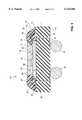
- FIG. 1is a cross-sectional side view of an exemplary integrated circuit package 10 in accordance with the present invention.
- Substrate 11forms an insulating base of package 10.
- Substrate 11has an upper first surface 12 and a lower second surface 13.
- Substrate 11may be formed, for example, of a conventional epoxy laminate or ceramic. Examples of suitable substrates include Mitsubishi BT, Arlon 45N, and Nelco BT laminate substrates.
- An exemplary thickness of substrate 11, between first surface 12 and second surface 13,is between 0.36 mm and 0.56 mm, but the thickness of substrate 11 may vary depending on the application.
- the perimeter of substrate 11may be a variety of shapes, again depending on the packaging application. For example, the perimeter of substrate 11 may be square or rectangular.
- Integrated circuit die 14rests on and is affixed to first surface 12 of substrate 11.
- Die 14has an upper first surface 21 containing peripheral bonding pads 19, peripheral side surfaces 22, and a lower second surface 23 opposite first surface 21.
- Conventional epoxy die attach compoundsuch as QMI 696 available from the QMI Company of San Diego, Calif., may be used to affix lower second surface 23 of die 14 to first surface 12 of substrate 11.
- EPROM, CCD or other optical integrated circuit dieshave vision cells or other light-sensitive circuitry on their upper surfaces, which must be selectively or continuously exposed to light of a selected frequency for some functioning of the completed device.
- vision cells or other light-sensitive circuitryis exemplified by polyimide vision cell 24 on a central portion of upper first surface 21 of die 14.
- Other non-optical circuitry, not shown in FIG. 1,may also be exposed on first surface 21 of die 14, depending on the application.
- conductive structures on or adjacent to first surface 12 of substrate 11electrically connect die 14 to metallized via 15.
- a first end of a metal trace 16is electrically connected to via 15.
- Metal trace 16extends laterally away from via 15, and its second end is electrically connected to a metal contact 17 on first surface 12 of substrate 11.
- electrically connectedis used broadly herein to mean a conductive path exists between the "electrically connected” structures, which may be due to a direct or indirect physical connection.
- Contact 17is electrically connected to a first end of a metal bond wire 18.
- An opposite second end of bond wire 18is electrically connected to a conductive bonding pad 19 on a peripheral portion of upper first surface 21 of die 14.
- Metal trace 16 and metal contact 17may be formed, for example, of copper that is plated on first surface 12 of substrate 11 using conventional electroplating methods.
- Bond wire 18may be formed of gold or aluminum.
- FIG. 1A typical package like FIG. 1 will have multiple metallized vias 15, metal traces 16, contacts 17, bond wires 18, and bonding pads 19, the number of which would depend on the application. For clarity, only two of each of these structures are shown in FIG. 1.
- Metallized via 15also intersects lower second surface 13 of substrate 11. At second surface 13, a first end of metal trace 31 is electrically connected to metallized via 15. Metal trace 31 extends laterally on lower second surface 13 away from via 15. A second end of metal trace 31 is electrically connected to a planar metal interconnection ball land (not shown), which is also formed on lower second surface 13 of substrate 11. A metallic solder interconnection ball 33 is joined to the land. Interconnection balls 33 are used to electrically connect package 10, and hence die 14, to external circuitry such as a circuit board. In alternative embodiments, an interconnection ball land may be formed on the lower second surface of the substrate around the metallized via, as opposed to a lateral distance from the via, so that an interconnection ball may be placed directly below the via.
- a typical package like FIG. 1would have multiple metal traces 31, metal lands, and interconnection balls 33 on the lower second surface 13 of its substrate 11, the number of which would depend on the packaging application. For clarity, only two of these structures are shown in FIG. 1.
- the interconnection balls 33 of FIG. 1are characteristic of a ball grid array ("BGA") package.
- Such interconnection ballsare generally arranged in an array pattern, such as X and Y axis rows of balls, on second surface 13 of substrate 11. The particular pattern selected may depend, for example, on the external circuitry to which package 10 is ultimately electrically connected.
- interconnections of the various conductive structures described aboveincluding metallized vias 15, metal traces 16 and 31, contacts 17, bond wires 18, metal lands, and interconnection balls 33, provide an electrically conductive path between bonding pads 19 of die 14 and interconnection balls 33.
- Metallized vias 15provide the portion of the conductive path that extends through substrate 11.
- bead 20is adjacent to and a covers the peripheral edges of die 14 on first surface 12 of substrate 11.
- Bead 20has a top first portion 25, an opposite lower second portion 26, a outer third portion 27, and an inner fourth portion 28 adjacent to die 14.
- Top first portion 25 of bead 20forms a peripheral portion of the top surface of package 10.
- Lower second portion 26 of bead 20is on and fixed to first surface 12 of substrate 11.
- Outer third portion 27 of bead 20forms the peripheral side walls of package 10.
- Inner fourth portion 28 of bead 20covers side surfaces 22 of die 14, as well as the outer periphery of upper first surface 21 of die 14, including the interconnections between bond wires 18 and bonding pads 19 on die 14.
- bead 20protectively covers each metal trace 16, contact 17, bond wire 18, and bonding pad 19 located on or adjacent to first surface 12 of substrate 11.
- Bead 20also covers side surfaces 22 of die 14 and the periphery of upper first surface 21 of die 14, including bonding pads 19.
- Bead 20does not, however, cover the central portion of upper first surface 21 of die 14 where polyimide vision cell 24 is located, to avoid interference with the light-sensitive functioning of vision cell 24.
- the height of bead 20 above first surface 12 of substrate 11exceeds the height of die 14 and bond wires 18 above first surface 12. Accordingly, bead 20 and upper first surface 21 of die 14 together form and define a cavity above die 14, into which a thin layer of transparent encapsulating material 29 is deposited.
- FIG. 2is a top view of an incomplete package 10, before a transparent encapsulant is placed onto die 14.
- bead 20surrounds die 14, contacting side surfaces 22 of die 14 all the way around die 14.
- bead 20also covers the periphery of upper first surface 21 of die 14, the periphery of first surface 21 of die 14 is shown by dashed lines.
- die 14 and bead 20are shown as having square perimeters in FIG. 2, the perimeters of die 14 and bead 20 may vary depending on the application. For example, die 14 and bead 20 may have rectangular perimeters.
- Bead 20is formed of a material that is adhesive.
- the material of bead 20should also be somewhat viscous and flowable when initially applied onto first surface 12 of substrate 11, but should be readily hardenable by air drying or heating or the like so that bead 20 forms solid, protective side and top surfaces of package 10.
- An example material useful for bead 20is epoxy, such as Ciba Nagase 9006 epoxy from the Ciba Nagase Company of Japan. Hardening of this epoxy is normally accomplished by heating for about 60 minutes at 150° C.
- Other suitable epoxy materials usable for bead 20include Hysol 4451 from Hysol Corporation of City of Industry, Calif.
- bead 20may be formed of a silicone rubber, such as silicon rubber number 3140 from the Dow Corning Company.
- a planar layer of transparent encapsulant 29covers first surface 21 of die 14, including the central portion of first surface 21 of die 14 where polyimide vision cell 24 is located. When hardened, encapsulant 29 forms a top exterior surface of package 10.
- Encapsulant 29is contained within the square-sided cavity above die 14 which was formed by first surface 21 of die 14 and that part of inner fourth portion 28 of bead 20 whose height above first surface 12 of substrate 11 is greater than the height of die 14 above first surface 12 of substrate 11.
- the exemplary planar upper first surface 30 of encapsulant 29is slightly lower, for example, about 0.005 mm lower, than top first portion 25 of bead 20, which may provide protection from abrasions to first surface 30.
- the appropriate thickness of the layer of encapsulant 29depends, for example, on the packaging application and the material chosen for encapsulant 29.
- a typical material appropriate for encapsulant 29has a light transmission value that is a function of its thickness.
- Encapsulant 29is formed of a material that is adhesive.
- the material of encapsulant 29should be somewhat viscous and flowable when initially applied onto first surface 21 of die 14, but should be hardenable so that the layer of encapsulant 29 forms a solid, protective top surface of package 10 adjacent to die 14.
- the EPROM, CCD, and other optical sensing device applications suited for a package such as FIG. 1require that a surface of the packaged die be selectively or continuously exposed to light of a selected frequency.
- the material chosen for encapsulant 29should be transparent to the particular frequency of light needed by the application.
- die 14has a polyimide vision cell 24 located on a central portion of first surface 21 of die 14.
- a vision cellrequires exposure to visible light.
- encapsulant 29is formed of a clear material, such as clear TEFLON® synthetic polymeric resin (polytetrafluoroethylene) from the E.I. Dupont Chemical Company, or an equivalent transparent, protective material.
- a layer of TEFLON® resin having a thickness of about 0.20 mmmay be hardened by heating at a temperature of about 150° C. for about 60 minutes.
- a layer of water white clear epoxymay be used for encapsulant 29.
- dimensions of a package like FIG. 1will vary with the particular packaging application.
- dimensions of components of package 10may include an approximately 10 mm ⁇ 10 mm square substrate 11; an approximate 8 mm by 8 mm square die 14; a bead 20 having an approximate 9 mm ⁇ 9 mm square perimeter; a bead 20 height between top first portion 25 and first surface 12 of substrate 11 ranging from approximately 0.60 mm to 0.80 mm; a bead 20 width between outer third portion 27 and side surfaces 22 of die 14 ranging from approximately 0.60 mm to 0.80 mm; and a relatively thin layer of a transparent encapsulant 29 having a thickness, i.e., a height between upper first surface 21 of die 14 and upper first surface 30 of encapsulant 29, ranging from approximately 0.10 mm to 0.30 mm.
- the thickness of encapsulant 29may be 0.20 mm. Again, such dimensions will vary with the packaging application. For example, larger dies typically require larger packages.
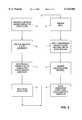
- FIG. 3shows a flow chart for an example method of making a package in accordance with the present invention.
- an insulating substrate baseis provided having conductive structures on and between its first and second surfaces.
- substrate 11 of FIG. 1is provided.
- substrate 11has metal traces 16 and 31, metallized vias 15, contacts 17, metal lands, and interconnection balls 33, all of which are electrically connected.
- an integrated circuit dieis provided and placed on the first surface of the substrate.
- a conventional epoxy die attach materialmay be used to affix the die to the substrate.
- the integrated circuit dieis electrically connected to the conductive structures on and through the substrate.
- bond wires 18are connected between bonding pads 19 on the periphery of die 14 and contacts 17 on substrate 11 so that die 15 may be electrically connected to metallized vias 15, and hence to interconnection balls 33.
- a conventional bond wire attaching machinemay be used to perform this step.
- a fourth step Dis the application of a bead of a viscous, hardenable, adhesive material onto the first surface of the substrate, around the integrated circuit die.
- the beadshould be applied so that its height relative to the upper first surface of the substrate exceeds the height of the die above the substrate. In this way, a cavity is formed above the upper first surface of the die into which the transparent encapsulant material may be deposited.
- FIGS. 1 and 2show an exemplary bead 20. In those figures, the bead was applied onto the substrate so as to cover the side surfaces of the die and the periphery of the upper first surface of die, as well as the bond wires and other conductive structures on the first surface of the substrate. The bead material does not cover the die's light-activated circuitry.
- An example bead materialis epoxy, such as Ciba Nagase 9006. Such an epoxy bead may be applied using a syringe. Alternatively, a conventional autodispense machine, such as model 5000 of the Camelot Company or the Millennium model of the Asymtek Company, may be used.
- a fifth step Eis to harden the bead material.
- the hardened bead materialforms solid, protective side and top surfaces of the package.
- FIG. 1shows an example of a solid bead 20.
- the step of hardening the bead materialmay be performed by heating to a temperature of approximately 150° C. for about 60 minutes.
- a sixth step Fis to apply a layer of a viscous, hardenable, adhesive, and selectively-transparent encapsulating material onto the exposed upper first surface of the die, within the three-dimensional cavity formed by the upper first surface of the die and the now-hardened bead material that surrounds the die.
- FIG. 1shows how an embodiment of a package appears after a layer of transparent encapsulant 29 is deposited onto upper first surface 21 of die 14.
- the encapsulating materialshould be clear so as to be transparent to visible light.
- An example materialis clear TEFLON® resin.
- the step of applying a layer of a selectively transparent encapsulating material onto the diemay be performed, for example, with a syringe or a conventional autodispense machine.
- the amount of encapsulating material usedaffects the thickness of the layer.
- a seventh step Gis to harden the layer of encapsulating material applied onto the die.
- This hardening stepis performed so that the encapsulating material forms a solid and protective top exterior surface of the package.
- This hardening stepmay be performed, for example, by heating the package after the encapsulating material is applied.
- conductive structuressuch as solder interconnection balls are placed by conventional methods onto metallizations provided on the underside of the substrate of the package.
- FIG. 1shows a package 10 having solder interconnection balls 33 on second surface 13 of substrate 11.
- such conductive structurescould be initially provided on the substrate.
- an array of packages similar to those of FIGS. 1-2are created on a single, relatively larger substrate, and then the array is cut apart to separate the individual packages from each other.
- FIG. 4is a top view of an array 40 of four incomplete packages 10 before the step of applying bead material is performed. While array 40 shows only four incomplete packages, the number of packages in the array can vary, depending, for example, on the size of the substrate and dies.
- the first three steps A-C of FIG. 3are performed, i.e. providing an insulating substrate having conductive structures, providing and affixing an integrated circuit die to the substrate, and electrically connecting the die to the conductive structures on the substrate, except that a larger substrate 41 having four sites for placement of integrated circuit dies is provided, and the other steps are repeated to accommodate each of the four integrated circuit dies that are affixed to substrate 41.
- a fourth stepis to apply a square bead, like bead 20 in FIGS. 1 and 2, peripherally around each die on array 40 of FIG. 4.
- the step of applying a bead of adhesive materialis performed by applying a first set of parallel beads of adhesive material adjacent to the integrated circuit dies, and then applying a second set of parallel beads of adhesive material perpendicularly across the first set of parallel beads, so that a crisscrossing pattern of rows and columns of bead material is deposited on the substrate around all sides of each die.
- the crisscrossing beadsmeld to form a continuous bead around each die in the array.
- the bead and the upper first surface of the dietogether define a cavity above the die, into which the layer of encapsulating material is deposited.
- the fifth through eighth steps E-H of FIG. 3are performed for each package in the array, i.e. the steps of hardening the beads, applying the layers of encapsulant within the cavities formed by the beads, hardening the layers of encapsulant, and placing conductive structures such as interconnection balls on the second surface of the substrate for each site on the array.
- a step of separating the individual packages in the array of packages from each otheris performed. This step may be performed, for example, by cutting through the substrate and bead material using a conventional wafer saw.
Landscapes
- Engineering & Computer Science (AREA)
- Computer Hardware Design (AREA)
- Microelectronics & Electronic Packaging (AREA)
- Power Engineering (AREA)
- Solid State Image Pick-Up Elements (AREA)
- Light Receiving Elements (AREA)
- Structures Or Materials For Encapsulating Or Coating Semiconductor Devices Or Solid State Devices (AREA)
Abstract
Description
Claims (46)
Priority Applications (1)
| Application Number | Priority Date | Filing Date | Title |
|---|---|---|---|
| US09/176,048US6143588A (en) | 1997-09-09 | 1998-10-20 | Method of making an integrated circuit package employing a transparent encapsulant |
Applications Claiming Priority (2)
| Application Number | Priority Date | Filing Date | Title |
|---|---|---|---|
| US08/926,507US5962810A (en) | 1997-09-09 | 1997-09-09 | Integrated circuit package employing a transparent encapsulant |
| US09/176,048US6143588A (en) | 1997-09-09 | 1998-10-20 | Method of making an integrated circuit package employing a transparent encapsulant |
Related Parent Applications (1)
| Application Number | Title | Priority Date | Filing Date |
|---|---|---|---|
| US08/926,507DivisionUS5962810A (en) | 1997-09-09 | 1997-09-09 | Integrated circuit package employing a transparent encapsulant |
Publications (1)
| Publication Number | Publication Date |
|---|---|
| US6143588Atrue US6143588A (en) | 2000-11-07 |
Family
ID=25453307
Family Applications (2)
| Application Number | Title | Priority Date | Filing Date |
|---|---|---|---|
| US08/926,507Expired - LifetimeUS5962810A (en) | 1997-09-09 | 1997-09-09 | Integrated circuit package employing a transparent encapsulant |
| US09/176,048Expired - LifetimeUS6143588A (en) | 1997-09-09 | 1998-10-20 | Method of making an integrated circuit package employing a transparent encapsulant |
Family Applications Before (1)
| Application Number | Title | Priority Date | Filing Date |
|---|---|---|---|
| US08/926,507Expired - LifetimeUS5962810A (en) | 1997-09-09 | 1997-09-09 | Integrated circuit package employing a transparent encapsulant |
Country Status (6)
| Country | Link |
|---|---|
| US (2) | US5962810A (en) |
| EP (1) | EP1018165A1 (en) |
| JP (1) | JP2001516956A (en) |
| KR (1) | KR20010023809A (en) |
| CA (1) | CA2301615A1 (en) |
| WO (1) | WO1999013515A1 (en) |
Cited By (112)
| Publication number | Priority date | Publication date | Assignee | Title |
|---|---|---|---|---|
| US20020081780A1 (en)* | 2000-08-17 | 2002-06-27 | Authen Tec | Methods and apparatus for making integrated circuit package including opening exposing portion of the IC |
| US6420204B2 (en) | 1999-06-03 | 2002-07-16 | Amkor Technology, Inc. | Method of making a plastic package for an optical integrated circuit device |
| US6509560B1 (en) | 2000-11-13 | 2003-01-21 | Amkor Technology, Inc. | Chip size image sensor in wirebond package with step-up ring for electrical contact |
| US6528857B1 (en)* | 2000-11-13 | 2003-03-04 | Amkor Technology, Inc. | Chip size image sensor bumped package |
| US6531333B2 (en) | 2000-04-05 | 2003-03-11 | Hong-Ming Lin | Chip photoelectric sensor assembly and method for making same |
| US6564454B1 (en) | 2000-12-28 | 2003-05-20 | Amkor Technology, Inc. | Method of making and stacking a semiconductor package |
| US6576539B1 (en) | 2000-10-13 | 2003-06-10 | Charles W.C. Lin | Semiconductor chip assembly with interlocked conductive trace |
| US20030127654A1 (en)* | 2000-02-15 | 2003-07-10 | Dominik Eisert | Semiconductor component which emits radiation, and method for producing the same |
| US20030143781A1 (en)* | 2002-01-31 | 2003-07-31 | Mclellan Neil Robert | Encapsulated integrated circuit package and method of manufacturing an integrated circuit package |
| US20030159278A1 (en)* | 2002-02-26 | 2003-08-28 | Peddle Charles I. | Methods and apparatus for fabricating Chip-on-Board modules |
| US20030164502A1 (en)* | 2000-05-23 | 2003-09-04 | Johannes Baur | Optoelectronic component and a method for producing the same |
| US6620646B1 (en) | 2000-11-13 | 2003-09-16 | Amkor Technology, Inc. | Chip size image sensor wirebond package fabrication method |
| US6629633B1 (en) | 2000-11-13 | 2003-10-07 | Amkor Technology, Inc. | Chip size image sensor bumped package fabrication method |
| US20030234454A1 (en)* | 2002-06-24 | 2003-12-25 | Serafin Pedron | Integrated circuit package and method of manufacturing the integrated circuit package |
| US6686667B2 (en)* | 2002-04-22 | 2004-02-03 | Scientek Corp. | Image sensor semiconductor package with castellation |
| US20040038442A1 (en)* | 2002-08-26 | 2004-02-26 | Kinsman Larry D. | Optically interactive device packages and methods of assembly |
| US6716670B1 (en) | 2002-01-09 | 2004-04-06 | Bridge Semiconductor Corporation | Method of forming a three-dimensional stacked semiconductor package device |
| US20040080037A1 (en)* | 2002-10-25 | 2004-04-29 | Foong Chee Seng | Image sensor device |
| US6734552B2 (en) | 2001-07-11 | 2004-05-11 | Asat Limited | Enhanced thermal dissipation integrated circuit package |
| US20040129991A1 (en)* | 2002-09-25 | 2004-07-08 | Lai Jay Jie | Front side illuminated photodiode with backside bump |
| US20040150064A1 (en)* | 2001-04-11 | 2004-08-05 | Lutz Rissling | Optoelectronic component array and method for the production of an optoelectronic component array |
| US20050003565A1 (en)* | 2000-02-15 | 2005-01-06 | Osram Opto Semiconductors Gmbh, A Germany Corporat | Radiation emitting semiconductor device |
| US20050009239A1 (en)* | 2003-07-07 | 2005-01-13 | Wolff Larry Lee | Optoelectronic packaging with embedded window |
| US20050059188A1 (en)* | 2003-09-17 | 2005-03-17 | Bolken Todd O. | Image sensor packages and methods of fabrication |
| US6893169B1 (en)* | 1999-11-04 | 2005-05-17 | Stmicroelectronics S.A. | Optical semiconductor package and process for fabricating the same |
| US20050110889A1 (en)* | 2003-11-26 | 2005-05-26 | Tuttle Mark E. | Packaged microelectronic imagers and methods of packaging microelectronic imagers |
| US6905910B1 (en) | 2004-01-06 | 2005-06-14 | Freescale Semiconductor, Inc. | Method of packaging an optical sensor |
| US20050184219A1 (en)* | 2004-02-23 | 2005-08-25 | Kirby Kyle K. | Packaged microelectronic imagers and methods of packaging microelectronic imagers |
| US6936495B1 (en) | 2002-01-09 | 2005-08-30 | Bridge Semiconductor Corporation | Method of making an optoelectronic semiconductor package device |
| US20050255628A1 (en)* | 2003-09-18 | 2005-11-17 | Micron Technology, Inc. | Microelectronic devices and methods for packaging microelectronic devices |
| US20050254133A1 (en)* | 2004-05-13 | 2005-11-17 | Salman Akram | Integrated optics units and methods of manufacturing integrated optics units for use with microelectronic imagers |
| US20050270055A1 (en)* | 2004-06-02 | 2005-12-08 | Salman Akram | Systems and methods for testing microelectronic imagers and microfeature devices |
| US20050275049A1 (en)* | 2004-06-10 | 2005-12-15 | Kirby Kyle K | Packaged microelectronic imagers and methods of packging microelectronic imagers |
| US20050275750A1 (en)* | 2004-06-09 | 2005-12-15 | Salman Akram | Wafer-level packaged microelectronic imagers and processes for wafer-level packaging |
| US20050275051A1 (en)* | 2004-06-14 | 2005-12-15 | Farnworth Warren M | Prefabricated housings for microelectronic imagers and methods for packaging microelectronic imagers |
| US20050275048A1 (en)* | 2004-06-14 | 2005-12-15 | Farnworth Warren M | Microelectronic imagers and methods of packaging microelectronic imagers |
| US20050285154A1 (en)* | 2004-06-29 | 2005-12-29 | Salman Akram | Packaged microelectronic imagers and methods of packaging microelectronic imagers |
| US6987034B1 (en) | 2002-01-09 | 2006-01-17 | Bridge Semiconductor Corporation | Method of making a semiconductor package device that includes singulating and trimming a lead |
| US20060011809A1 (en)* | 2004-07-19 | 2006-01-19 | Farnworth Warren M | Microelectronic imagers with optical devices and methods of manufacturing such microelectronic imagers |
| US20060014313A1 (en)* | 2004-07-16 | 2006-01-19 | Hall Frank L | Microelectronic imaging units and methods of manufacturing microelectronic imaging units |
| US20060024856A1 (en)* | 2004-07-28 | 2006-02-02 | Derderian James M | Microelectronic imaging units and methods of manufacturing microelectronic imaging units |
| US20060038183A1 (en)* | 2004-08-19 | 2006-02-23 | Oliver Steven D | Microelectronic imagers with curved image sensors and methods for manufacturing microelectronic imagers |
| US20060040421A1 (en)* | 2004-08-19 | 2006-02-23 | Farnworth Warren M | Spacers for packaged microelectronic imagers and methods of making and using spacers for wafer-level packaging of imagers |
| US20060046332A1 (en)* | 2004-08-26 | 2006-03-02 | Derderian James M | Microelectronic Imaging units and methods of manufacturing microelectronic imaging units |
| US20060043509A1 (en)* | 2004-08-24 | 2006-03-02 | Watkins Charles M | Packaged microelectronic imaging devices and methods of packaging microelectronic imaging devices |
| US20060043262A1 (en)* | 2004-08-30 | 2006-03-02 | Micron Technology, Inc. | Microelectronic imagers with integrated optical devices and methods for manufacturing such microelectronic imagers |
| US20060043277A1 (en)* | 2004-08-24 | 2006-03-02 | Tai Li C | Integrated ball grid array optical mouse sensor packaging |
| US20060043512A1 (en)* | 2004-08-24 | 2006-03-02 | Oliver Steven D | Microelectronic imagers with optical devices having integral reference features and methods for manufacturing such microelectronic imagers |
| US20060044433A1 (en)* | 2004-08-31 | 2006-03-02 | Micron Technology, Inc. | Microelectronic imagers having front side contacts and methods of packaging such microelectronic imagers |
| US20060043599A1 (en)* | 2004-09-02 | 2006-03-02 | Salman Akram | Through-wafer interconnects for photoimager and memory wafers |
| US7015072B2 (en) | 2001-07-11 | 2006-03-21 | Asat Limited | Method of manufacturing an enhanced thermal dissipation integrated circuit package |
| US20060148250A1 (en)* | 2004-12-30 | 2006-07-06 | Micron Technology, Inc. | Methods for forming interconnects in microelectronic workpieces and microelectronic workpieces formed using such methods |
| US20060175532A1 (en)* | 2005-02-08 | 2006-08-10 | Micron Technology, Inc. | Microelectronic imaging units and methods of manufacturing microelectronic imaging units |
| US20060177959A1 (en)* | 2005-02-10 | 2006-08-10 | Micron Technology, Inc. | Microfeature workpieces having microlenses and methods of forming microlenses on microfeature workpieces |
| US20060177999A1 (en)* | 2005-02-10 | 2006-08-10 | Micron Technology, Inc. | Microelectronic workpieces and methods for forming interconnects in microelectronic workpieces |
| US20060186492A1 (en)* | 2005-02-18 | 2006-08-24 | Micron Technology, Inc. | Microelectronic imagers with shaped image sensors and methods for manufacturing microelectronic imagers |
| US20060216850A1 (en)* | 2004-08-10 | 2006-09-28 | Street Bret K | Microelectronic imaging units and methods of manufacturing microelectronic imaging units |
| US20060289968A1 (en)* | 2005-06-28 | 2006-12-28 | Micron Technology, Inc. | Conductive interconnect structures and formation methods using supercritical fluids |
| US20070045858A1 (en)* | 2005-09-01 | 2007-03-01 | Micron Technology, Inc. | Microfeature workpieces and methods for forming interconnects in microfeature workpieces |
| US20070045515A1 (en)* | 2005-09-01 | 2007-03-01 | Micron Technology, Inc. | Microelectronic imaging devices and associated methods for attaching transmissive elements |
| US7190060B1 (en) | 2002-01-09 | 2007-03-13 | Bridge Semiconductor Corporation | Three-dimensional stacked semiconductor package device with bent and flat leads and method of making same |
| US20070057169A1 (en)* | 2005-09-14 | 2007-03-15 | Chung-Chi Hsiao | Package structure for an optical sensor |
| US20070102832A1 (en)* | 2005-07-27 | 2007-05-10 | Texas Instruments Incorporated | Plastic Semiconductor Package Having Improved Control of Dimensions |
| US7232754B2 (en) | 2004-06-29 | 2007-06-19 | Micron Technology, Inc. | Microelectronic devices and methods for forming interconnects in microelectronic devices |
| US20070148807A1 (en)* | 2005-08-22 | 2007-06-28 | Salman Akram | Microelectronic imagers with integrated optical devices and methods for manufacturing such microelectronic imagers |
| US20070158833A1 (en)* | 2006-01-04 | 2007-07-12 | Soo-San Park | Integrated circuit package system including stacked die |
| US20070158809A1 (en)* | 2006-01-04 | 2007-07-12 | Chow Seng G | Multi-chip package system |
| US20070166867A1 (en)* | 2006-01-04 | 2007-07-19 | Chow Seng G | Integrated circuit package system with image sensor system |
| US20070182018A1 (en)* | 2006-02-09 | 2007-08-09 | Stats Chippac Ltd. | Integrated circuit package system including zero fillet resin |
| US20070190690A1 (en)* | 2006-02-14 | 2007-08-16 | Stats Chippac Ltd. | Integrated circuit package system with exposed interconnects |
| US7268368B1 (en) | 2003-08-29 | 2007-09-11 | Standard Microsystems Corporation | Semiconductor package having optical receptacles and light transmissive/opaque portions and method of making same |
| US20070251719A1 (en)* | 2006-04-27 | 2007-11-01 | Rick Sturdivant | Selective, hermetically sealed microwave package apparatus and methods |
| US7413979B2 (en) | 2003-11-13 | 2008-08-19 | Micron Technology, Inc. | Methods for forming vias in microelectronic devices, and methods for packaging microelectronic devices |
| US7425499B2 (en) | 2004-08-24 | 2008-09-16 | Micron Technology, Inc. | Methods for forming interconnects in vias and microelectronic workpieces including such interconnects |
| US7435913B2 (en) | 2004-08-27 | 2008-10-14 | Micron Technology, Inc. | Slanted vias for electrical circuits on circuit boards and other substrates |
| US7448910B2 (en) | 2004-09-03 | 2008-11-11 | Samsung Electronics Co., Ltd | Displaying apparatus |
| US20090032972A1 (en)* | 2007-03-30 | 2009-02-05 | Kabushiki Kaisha Toshiba | Semiconductor device |
| US20090079097A1 (en)* | 2007-09-25 | 2009-03-26 | Silverbrook Research Pty Ltd | Electronic component with wire bonds in low modulus fill encapsulant |
| US20090079793A1 (en)* | 2007-09-25 | 2009-03-26 | Silverbrook Research Pty Ltd | Integrated circuit support for low profile wire bond |
| US20090081832A1 (en)* | 2007-09-25 | 2009-03-26 | Silverbrook Research Pty Ltd | Method of reducing wire bond profile height in integrated circuits mounted to circuit boards |
| US20090079081A1 (en)* | 2007-09-25 | 2009-03-26 | Silverbrook Research Pty Ltd | Electronic device with wire bonds adhered between integrated circuits dies and printed circuit boards |
| US20090081829A1 (en)* | 2007-09-25 | 2009-03-26 | Silverbrook Research Pty Ltd | Method of adhering wire bond loops to reduce loop height |
| US20090078744A1 (en)* | 2007-09-25 | 2009-03-26 | Silverbrook Research Pty Ltd | Method of forming low profile wire bonds between integrated circuits dies and printed circuit boards |
| US20090081834A1 (en)* | 2007-09-25 | 2009-03-26 | Silverbrook Research Pty Ltd | Method of applying encapsulant to wire bonds |
| WO2009039550A1 (en)* | 2007-09-25 | 2009-04-02 | Silverbrook Research Pty Ltd | Method of wire bond encapsulation profiling |
| US20090102002A1 (en)* | 2007-10-23 | 2009-04-23 | Micron Technology, Inc. | Packaged semiconductor assemblies and associated systems and methods |
| US20090135569A1 (en)* | 2007-09-25 | 2009-05-28 | Silverbrook Research Pty Ltd | Electronic component with wire bonds in low modulus fill encapsulant |
| US7622377B2 (en) | 2005-09-01 | 2009-11-24 | Micron Technology, Inc. | Microfeature workpiece substrates having through-substrate vias, and associated methods of formation |
| US7629249B2 (en) | 2006-08-28 | 2009-12-08 | Micron Technology, Inc. | Microfeature workpieces having conductive interconnect structures formed by chemically reactive processes, and associated systems and methods |
| US7659141B2 (en) | 2007-09-25 | 2010-02-09 | Silverbrook Research Pty Ltd | Wire bond encapsulant application control |
| US7687315B2 (en) | 2005-04-29 | 2010-03-30 | Stats Chippac Ltd. | Stacked integrated circuit package system and method of manufacture therefor |
| US20100147377A1 (en)* | 2008-12-11 | 2010-06-17 | Seiji Ishihara | Solar cell module and method for producing the same |
| US20100167451A1 (en)* | 2007-04-05 | 2010-07-01 | Micron Technology, Inc. | Methods of manufacturing imaging device packages |
| US20100164081A1 (en)* | 2008-12-29 | 2010-07-01 | Texas Instruments Incorporated | Micro-Optical Device Packaging System |
| US7749899B2 (en) | 2006-06-01 | 2010-07-06 | Micron Technology, Inc. | Microelectronic workpieces and methods and systems for forming interconnects in microelectronic workpieces |
| US20100194465A1 (en)* | 2009-02-02 | 2010-08-05 | Ali Salih | Temperature compensated current source and method therefor |
| US7830018B2 (en) | 2007-08-31 | 2010-11-09 | Micron Technology, Inc. | Partitioned through-layer via and associated systems and methods |
| US7855100B2 (en) | 2005-03-31 | 2010-12-21 | Stats Chippac Ltd. | Integrated circuit package system with an encapsulant cavity and method of fabrication thereof |
| US7863187B2 (en) | 2005-09-01 | 2011-01-04 | Micron Technology, Inc. | Microfeature workpieces and methods for forming interconnects in microfeature workpieces |
| US20110001208A1 (en)* | 2008-03-11 | 2011-01-06 | Junya Furuyashiki | Semiconductor device and semiconductor device manufacturing method |
| US20110024920A1 (en)* | 2008-04-03 | 2011-02-03 | Dr. Johannes Heidenhain Gmbh | Component arrangement and method for producing a component arrangement |
| US7884015B2 (en) | 2007-12-06 | 2011-02-08 | Micron Technology, Inc. | Methods for forming interconnects in microelectronic workpieces and microelectronic workpieces formed using such methods |
| US7902643B2 (en) | 2006-08-31 | 2011-03-08 | Micron Technology, Inc. | Microfeature workpieces having interconnects and conductive backplanes, and associated systems and methods |
| US8025204B2 (en) | 2007-09-25 | 2011-09-27 | Silverbrook Research Pty Ltd | Method of wire bond encapsulation profiling |
| US8084866B2 (en) | 2003-12-10 | 2011-12-27 | Micron Technology, Inc. | Microelectronic devices and methods for filling vias in microelectronic devices |
| US8092734B2 (en) | 2004-05-13 | 2012-01-10 | Aptina Imaging Corporation | Covers for microelectronic imagers and methods for wafer-level packaging of microelectronics imagers |
| US20130200503A1 (en)* | 2012-02-08 | 2013-08-08 | Carsem (M) Sdn, Bhd. | Protective layers in semiconductor packaging |
| US8536485B2 (en) | 2004-05-05 | 2013-09-17 | Micron Technology, Inc. | Systems and methods for forming apertures in microfeature workpieces |
| US8652866B2 (en)* | 2009-03-12 | 2014-02-18 | Infineon Technologies Ag | Sensor device and method |
| US20150179828A1 (en)* | 2009-09-24 | 2015-06-25 | Msg Lithoglas Ag | Arrangement with a component on a carrier substrate, an arrangement and a semi-finished product |
| US9722098B1 (en) | 2016-10-18 | 2017-08-01 | Ase Electronics (M) Sdn Bhd | Semiconductor device package and method of manufacturing the same |
| WO2018059873A1 (en)* | 2016-09-30 | 2018-04-05 | Robert Bosch Gmbh | Method for producing an electronic assembly, and electronic assembly, in particular for a transmission control module |
Families Citing this family (66)
| Publication number | Priority date | Publication date | Assignee | Title |
|---|---|---|---|---|
| US6962829B2 (en) | 1996-10-31 | 2005-11-08 | Amkor Technology, Inc. | Method of making near chip size integrated circuit package |
| JPH1197656A (en)* | 1997-09-22 | 1999-04-09 | Fuji Electric Co Ltd | Semiconductor optical sensor device |
| US6092281A (en) | 1998-08-28 | 2000-07-25 | Amkor Technology, Inc. | Electromagnetic interference shield driver and method |
| US6301401B1 (en)* | 1999-04-02 | 2001-10-09 | Convergence Technologies, Ltd. | Electro-optical package for reducing parasitic effects |
| US6232551B1 (en)* | 1999-08-18 | 2001-05-15 | Subtron Technology Co., Ltd. | Substrate board for semiconductor package |
| WO2001015237A1 (en)* | 1999-08-20 | 2001-03-01 | Amkor Technology, Inc. | Chip-sized optical sensor package |
| US6448635B1 (en) | 1999-08-30 | 2002-09-10 | Amkor Technology, Inc. | Surface acoustical wave flip chip |
| FR2800909B1 (en)* | 1999-11-04 | 2003-08-22 | St Microelectronics Sa | OPTICAL SEMICONDUCTOR PACKAGE AND METHOD FOR MANUFACTURING SUCH A PACKAGE |
| US6841412B1 (en)* | 1999-11-05 | 2005-01-11 | Texas Instruments Incorporated | Encapsulation for particle entrapment |
| US6627864B1 (en) | 1999-11-22 | 2003-09-30 | Amkor Technology, Inc. | Thin image sensor package |
| US6396043B1 (en) | 1999-11-22 | 2002-05-28 | Amkor Technology, Inc. | Thin image sensor package fabrication method |
| JP2001208509A (en)* | 2000-01-24 | 2001-08-03 | Sony Corp | Semiconductor device for confirming surface shape and method for manufacturing the same |
| JP3651577B2 (en) | 2000-02-23 | 2005-05-25 | 三菱電機株式会社 | Imaging device |
| US6571466B1 (en) | 2000-03-27 | 2003-06-03 | Amkor Technology, Inc. | Flip chip image sensor package fabrication method |
| US6518659B1 (en) | 2000-05-08 | 2003-02-11 | Amkor Technology, Inc. | Stackable package having a cavity and a lid for an electronic device |
| US6424031B1 (en) | 2000-05-08 | 2002-07-23 | Amkor Technology, Inc. | Stackable package with heat sink |
| US6667544B1 (en) | 2000-06-30 | 2003-12-23 | Amkor Technology, Inc. | Stackable package having clips for fastening package and tool for opening clips |
| US7273769B1 (en) | 2000-08-16 | 2007-09-25 | Micron Technology, Inc. | Method and apparatus for removing encapsulating material from a packaged microelectronic device |
| US6849916B1 (en) | 2000-11-15 | 2005-02-01 | Amkor Technology, Inc. | Flip chip on glass sensor package |
| US6342406B1 (en) | 2000-11-15 | 2002-01-29 | Amkor Technology, Inc. | Flip chip on glass image sensor package fabrication method |
| US6541837B2 (en)* | 2001-02-09 | 2003-04-01 | International Business Machines Corporation | Charge-coupled device wafer cover plate with compact interconnect wiring |
| US6861720B1 (en) | 2001-08-29 | 2005-03-01 | Amkor Technology, Inc. | Placement template and method for placing optical dies |
| JP4000507B2 (en)* | 2001-10-04 | 2007-10-31 | ソニー株式会社 | Method for manufacturing solid-state imaging device |
| US20050051859A1 (en)* | 2001-10-25 | 2005-03-10 | Amkor Technology, Inc. | Look down image sensor package |
| JP2003198897A (en)* | 2001-12-27 | 2003-07-11 | Seiko Epson Corp | Optical module, circuit board and electronic equipment |
| US6784534B1 (en) | 2002-02-06 | 2004-08-31 | Amkor Technology, Inc. | Thin integrated circuit package having an optically transparent window |
| US6745462B2 (en) | 2002-03-07 | 2004-06-08 | Kulicke & Soffa Industries, Inc. | Method and apparatus for reducing deformation of encapsulant in semiconductor device encapsulation by stencil printing |
| JP4126389B2 (en)* | 2002-09-20 | 2008-07-30 | カシオ計算機株式会社 | Manufacturing method of semiconductor package |
| US6696738B1 (en)* | 2002-11-12 | 2004-02-24 | Kingpak Technology Inc. | Miniaturized image sensor |
| TWI311353B (en)* | 2003-04-18 | 2009-06-21 | Advanced Semiconductor Eng | Stacked chip package structure |
| US6809261B1 (en)* | 2003-06-23 | 2004-10-26 | Agilent Technologies, Inc. | Physically compact device package |
| US6977431B1 (en) | 2003-11-05 | 2005-12-20 | Amkor Technology, Inc. | Stackable semiconductor package and manufacturing method thereof |
| IL159032A0 (en)* | 2003-11-24 | 2004-05-12 | Safety Quick Light Ltd | Swivellable electric socket-plug combination |
| JP2007538347A (en)* | 2003-11-28 | 2007-12-27 | トムソン ライセンシング | Photoelectric transducer and method of manufacturing optical pickup |
| EP1619726A1 (en)* | 2004-07-22 | 2006-01-25 | St Microelectronics S.A. | Package for optical semiconductor detector |
| US20080203552A1 (en)* | 2005-02-15 | 2008-08-28 | Unisemicon Co., Ltd. | Stacked Package and Method of Fabricating the Same |
| TWI290763B (en)* | 2006-01-18 | 2007-12-01 | Siliconware Precision Industries Co Ltd | Semiconductor devices and fabrication method thereof |
| US7521728B2 (en)* | 2006-01-20 | 2009-04-21 | Cree, Inc. | Packages for semiconductor light emitting devices utilizing dispensed reflectors and methods of forming the same |
| CN100454505C (en)* | 2006-01-25 | 2009-01-21 | 矽品精密工业股份有限公司 | Semiconductor device and method for fabricating the same |
| JP3940423B1 (en)* | 2006-03-02 | 2007-07-04 | ソニーケミカル&インフォメーションデバイス株式会社 | Functional element mounting module and manufacturing method thereof |
| CN100461437C (en)* | 2006-03-07 | 2009-02-11 | 崴强科技股份有限公司 | Method for adjusting lens deviation of sensing element and packaging structure thereof |
| TW200822315A (en)* | 2006-11-03 | 2008-05-16 | Siliconware Precision Industries Co Ltd | Sensor type semiconductor package and fabrication method thereof |
| US8049237B2 (en)* | 2007-12-28 | 2011-11-01 | Nichia Corporation | Light emitting device |
| US20090166831A1 (en)* | 2007-12-28 | 2009-07-02 | Siliconware Precision Industries Co., Ltd. | Sensor semiconductor package and method for fabricating the same |
| US20090309238A1 (en)* | 2008-06-13 | 2009-12-17 | Mun Leong Loke | Molded flip chip package with enhanced mold-die adhesion |
| US8247827B2 (en)* | 2008-09-30 | 2012-08-21 | Bridgelux, Inc. | LED phosphor deposition |
| JP5417888B2 (en)* | 2009-02-24 | 2014-02-19 | 豊田合成株式会社 | Method for manufacturing light emitting device |
| US8071893B2 (en) | 2009-03-04 | 2011-12-06 | Apple Inc. | Methods and apparatus for shielding circuitry from interference |
| JP2013118206A (en)* | 2010-03-25 | 2013-06-13 | Panasonic Corp | Semiconductor device and manufacturing method of the same |
| US9406580B2 (en) | 2011-03-16 | 2016-08-02 | Synaptics Incorporated | Packaging for fingerprint sensors and methods of manufacture |
| JP2012199833A (en)* | 2011-03-22 | 2012-10-18 | Taiyo Yuden Co Ltd | Electronic component, electronic device, and manufacturing method of electronic component |
| US11215188B2 (en) | 2014-09-30 | 2022-01-04 | Sql Technologies Corp. | Apparatus including a combination of a ceiling fan and a heater with light effects |
| US10453825B2 (en)* | 2014-11-11 | 2019-10-22 | Cree, Inc. | Light emitting diode (LED) components and methods |
| WO2016183354A1 (en) | 2015-05-12 | 2016-11-17 | Kohen Ran Roland | Smart quick connect device for electrical fixtures |
| US9741633B2 (en) | 2015-06-02 | 2017-08-22 | Samsung Electronics Co., Ltd. | Semiconductor package including barrier members and method of manufacturing the same |
| ES2964013T3 (en) | 2017-03-05 | 2024-04-03 | Skyx Platforms Corp | Intelligent modular quick connect device for electrical accessories |
| EP3593418A4 (en) | 2017-03-10 | 2020-11-25 | Ran Roland Kohen | QUICK CONNECTION DEVICE FOR ELECTRIC RECESSED LUMINAIRES |
| US12284299B2 (en)* | 2017-03-16 | 2025-04-22 | Motorola Mobility Llc | Electronic device housing with insert molded features and methods of constructing the same |
| CA3060544A1 (en) | 2017-04-17 | 2018-10-25 | Ran Roland Kohen | Disconnecting and supporting quick release electrical fixtures |
| WO2018204313A1 (en) | 2017-05-01 | 2018-11-08 | Kohen Ran Roland | Connecting lighting to poles without tools |
| DE102018130510A1 (en)* | 2018-11-30 | 2020-06-04 | Vishay Semiconductor Gmbh | Radiation sensor and manufacturing process therefor |
| KR102786992B1 (en) | 2019-02-20 | 2025-03-27 | 에스케이와이엑스 플랫폼 코포레이션 | Cross release attachment quick connect device |
| CN110112163A (en)* | 2019-05-17 | 2019-08-09 | 积高电子(无锡)有限公司 | A kind of image sensor package structure and packaging method |
| US11276806B2 (en)* | 2020-01-03 | 2022-03-15 | Advanced Semiconductor Engineering, Inc. | Semiconductor device package and method for manufacturing the same |
| KR20220161324A (en) | 2020-02-28 | 2022-12-06 | 에스케이와이엑스 플랫폼 코포레이션 | Recessed Smart Quick Connect Device |
| JP7185157B2 (en)* | 2020-12-25 | 2022-12-07 | 日亜化学工業株式会社 | Light-emitting module and method for manufacturing light-emitting module |
Citations (27)
| Publication number | Priority date | Publication date | Assignee | Title |
|---|---|---|---|---|
| US4530152A (en)* | 1982-04-01 | 1985-07-23 | Compagnie Industrielle Des Telecommunications Cit-Alcatel | Method for encapsulating semiconductor components using temporary substrates |
| JPS629639A (en)* | 1985-07-05 | 1987-01-17 | Nec Yamagata Ltd | Manufacture of semiconductor device |
| US4649418A (en)* | 1982-09-27 | 1987-03-10 | U.S. Philips Corporation | Data card and method of manufacturing same |
| US4691225A (en)* | 1982-02-05 | 1987-09-01 | Hitachi, Ltd. | Semiconductor device and a method of producing the same |
| WO1989000337A1 (en)* | 1987-06-29 | 1989-01-12 | Eastman Kodak Company | Encapsulation barrier for thick-film hybrid circuits |
| US4801998A (en)* | 1984-08-20 | 1989-01-31 | Oki Electric Industry Co., Ltd. | EPROM device |
| US4890383A (en)* | 1988-01-15 | 1990-01-02 | Simens Corporate Research & Support, Inc. | Method for producing displays and modular components |
| US5043004A (en)* | 1990-08-29 | 1991-08-27 | Kyocera America, Inc. | Method for making a ceramic lid for hermetic sealing of an EPROM circuit |
| US5102829A (en)* | 1991-07-22 | 1992-04-07 | At&T Bell Laboratories | Plastic pin grid array package |
| US5126818A (en)* | 1987-05-26 | 1992-06-30 | Matsushita Electric Works, Ltd. | Semiconductor device |
| US5192681A (en)* | 1990-08-31 | 1993-03-09 | Texas Instruments Incorporated | Low cost erasable programmable read only memory package |
| JPH05218230A (en)* | 1992-01-30 | 1993-08-27 | Nec Corp | Semiconductor device |
| US5241133A (en)* | 1990-12-21 | 1993-08-31 | Motorola, Inc. | Leadless pad array chip carrier |
| US5250470A (en)* | 1989-12-22 | 1993-10-05 | Oki Electric Industry Co., Ltd. | Method for manufacturing a semiconductor device with corrosion resistant leads |
| US5336931A (en)* | 1993-09-03 | 1994-08-09 | Motorola, Inc. | Anchoring method for flow formed integrated circuit covers |
| US5436203A (en)* | 1994-07-05 | 1995-07-25 | Motorola, Inc. | Shielded liquid encapsulated semiconductor device and method for making the same |
| US5474957A (en)* | 1994-05-09 | 1995-12-12 | Nec Corporation | Process of mounting tape automated bonded semiconductor chip on printed circuit board through bumps |
| US5530278A (en)* | 1995-04-24 | 1996-06-25 | Xerox Corporation | Semiconductor chip having a dam to prevent contamination of photosensitive structures thereon |
| JPH08274219A (en)* | 1995-03-31 | 1996-10-18 | Seiko Epson Corp | Semiconductor device and manufacturing method thereof |
| US5578525A (en)* | 1993-12-13 | 1996-11-26 | Fujitsu Limited | Semiconductor device and a fabrication process thereof |
| US5593926A (en)* | 1993-10-12 | 1997-01-14 | Sumitomo Electric Industries, Ltd. | Method of manufacturing semiconductor device |
| US5612513A (en)* | 1995-09-19 | 1997-03-18 | Micron Communications, Inc. | Article and method of manufacturing an enclosed electrical circuit using an encapsulant |
| US5776798A (en)* | 1996-09-04 | 1998-07-07 | Motorola, Inc. | Semiconductor package and method thereof |
| US5861680A (en)* | 1995-09-29 | 1999-01-19 | Sony Corporation | Photonic device and process for fabricating the same |
| US5866953A (en)* | 1996-05-24 | 1999-02-02 | Micron Technology, Inc. | Packaged die on PCB with heat sink encapsulant |
| US5893723A (en)* | 1994-08-31 | 1999-04-13 | Sony Corporation | Manufacturing method for semiconductor unit |
| US5918113A (en)* | 1996-07-19 | 1999-06-29 | Shinko Electric Industries Co., Ltd. | Process for producing a semiconductor device using anisotropic conductive adhesive |
Family Cites Families (3)
| Publication number | Priority date | Publication date | Assignee | Title |
|---|---|---|---|---|
| US4814943A (en)* | 1986-06-04 | 1989-03-21 | Oki Electric Industry Co., Ltd. | Printed circuit devices using thermoplastic resin cover plate |
| EP0355522B1 (en)* | 1988-08-18 | 1993-12-15 | Seiko Epson Corporation | Solid state image pickup device |
| US5428188A (en)* | 1992-10-09 | 1995-06-27 | U.S. Terminals, Inc. | Low-cost package for electronic components |
- 1997
- 1997-09-09USUS08/926,507patent/US5962810A/ennot_activeExpired - Lifetime
- 1998
- 1998-09-04CACA002301615Apatent/CA2301615A1/ennot_activeAbandoned
- 1998-09-04EPEP98946800Apatent/EP1018165A1/ennot_activeCeased
- 1998-09-04WOPCT/US1998/017999patent/WO1999013515A1/ennot_activeApplication Discontinuation
- 1998-09-04KRKR1020007002483Apatent/KR20010023809A/ennot_activeCeased
- 1998-09-04JPJP2000511199Apatent/JP2001516956A/enactivePending
- 1998-10-20USUS09/176,048patent/US6143588A/ennot_activeExpired - Lifetime
Patent Citations (27)
| Publication number | Priority date | Publication date | Assignee | Title |
|---|---|---|---|---|
| US4691225A (en)* | 1982-02-05 | 1987-09-01 | Hitachi, Ltd. | Semiconductor device and a method of producing the same |
| US4530152A (en)* | 1982-04-01 | 1985-07-23 | Compagnie Industrielle Des Telecommunications Cit-Alcatel | Method for encapsulating semiconductor components using temporary substrates |
| US4649418A (en)* | 1982-09-27 | 1987-03-10 | U.S. Philips Corporation | Data card and method of manufacturing same |
| US4801998A (en)* | 1984-08-20 | 1989-01-31 | Oki Electric Industry Co., Ltd. | EPROM device |
| JPS629639A (en)* | 1985-07-05 | 1987-01-17 | Nec Yamagata Ltd | Manufacture of semiconductor device |
| US5126818A (en)* | 1987-05-26 | 1992-06-30 | Matsushita Electric Works, Ltd. | Semiconductor device |
| WO1989000337A1 (en)* | 1987-06-29 | 1989-01-12 | Eastman Kodak Company | Encapsulation barrier for thick-film hybrid circuits |
| US4890383A (en)* | 1988-01-15 | 1990-01-02 | Simens Corporate Research & Support, Inc. | Method for producing displays and modular components |
| US5250470A (en)* | 1989-12-22 | 1993-10-05 | Oki Electric Industry Co., Ltd. | Method for manufacturing a semiconductor device with corrosion resistant leads |
| US5043004A (en)* | 1990-08-29 | 1991-08-27 | Kyocera America, Inc. | Method for making a ceramic lid for hermetic sealing of an EPROM circuit |
| US5192681A (en)* | 1990-08-31 | 1993-03-09 | Texas Instruments Incorporated | Low cost erasable programmable read only memory package |
| US5241133A (en)* | 1990-12-21 | 1993-08-31 | Motorola, Inc. | Leadless pad array chip carrier |
| US5102829A (en)* | 1991-07-22 | 1992-04-07 | At&T Bell Laboratories | Plastic pin grid array package |
| JPH05218230A (en)* | 1992-01-30 | 1993-08-27 | Nec Corp | Semiconductor device |
| US5336931A (en)* | 1993-09-03 | 1994-08-09 | Motorola, Inc. | Anchoring method for flow formed integrated circuit covers |
| US5593926A (en)* | 1993-10-12 | 1997-01-14 | Sumitomo Electric Industries, Ltd. | Method of manufacturing semiconductor device |
| US5578525A (en)* | 1993-12-13 | 1996-11-26 | Fujitsu Limited | Semiconductor device and a fabrication process thereof |
| US5474957A (en)* | 1994-05-09 | 1995-12-12 | Nec Corporation | Process of mounting tape automated bonded semiconductor chip on printed circuit board through bumps |
| US5436203A (en)* | 1994-07-05 | 1995-07-25 | Motorola, Inc. | Shielded liquid encapsulated semiconductor device and method for making the same |
| US5893723A (en)* | 1994-08-31 | 1999-04-13 | Sony Corporation | Manufacturing method for semiconductor unit |
| JPH08274219A (en)* | 1995-03-31 | 1996-10-18 | Seiko Epson Corp | Semiconductor device and manufacturing method thereof |
| US5530278A (en)* | 1995-04-24 | 1996-06-25 | Xerox Corporation | Semiconductor chip having a dam to prevent contamination of photosensitive structures thereon |
| US5612513A (en)* | 1995-09-19 | 1997-03-18 | Micron Communications, Inc. | Article and method of manufacturing an enclosed electrical circuit using an encapsulant |
| US5861680A (en)* | 1995-09-29 | 1999-01-19 | Sony Corporation | Photonic device and process for fabricating the same |
| US5866953A (en)* | 1996-05-24 | 1999-02-02 | Micron Technology, Inc. | Packaged die on PCB with heat sink encapsulant |
| US5918113A (en)* | 1996-07-19 | 1999-06-29 | Shinko Electric Industries Co., Ltd. | Process for producing a semiconductor device using anisotropic conductive adhesive |
| US5776798A (en)* | 1996-09-04 | 1998-07-07 | Motorola, Inc. | Semiconductor package and method thereof |
Non-Patent Citations (4)
| Title |
|---|
| Banerji, K., "Development of the Slightly Larger Than IC Carrier (SLICC)", Proceedings of the Feb. 27-Mar. 4, 1994, Technical Program NEPCON WEST '94, pp. 1249-1256. |
| Banerji, K., Development of the Slightly Larger Than IC Carrier (SLICC) , Proceedings of the Feb. 27 Mar. 4, 1994, Technical Program NEPCON WEST 94, pp. 1249 1256.* |
| Levine, B. and Guinther, F., "The Package", Electronic News, vol. 42, No. 2112 (1996), pp. 1, 32. |
| Levine, B. and Guinther, F., The Package , Electronic News , vol. 42, No. 2112 (1996), pp. 1, 32.* |
Cited By (291)
| Publication number | Priority date | Publication date | Assignee | Title |
|---|---|---|---|---|
| US6420204B2 (en) | 1999-06-03 | 2002-07-16 | Amkor Technology, Inc. | Method of making a plastic package for an optical integrated circuit device |
| US6893169B1 (en)* | 1999-11-04 | 2005-05-17 | Stmicroelectronics S.A. | Optical semiconductor package and process for fabricating the same |
| US7195942B2 (en)* | 2000-02-15 | 2007-03-27 | Osram Gmbh | Radiation emitting semiconductor device |
| US20050003565A1 (en)* | 2000-02-15 | 2005-01-06 | Osram Opto Semiconductors Gmbh, A Germany Corporat | Radiation emitting semiconductor device |
| US20070145402A1 (en)* | 2000-02-15 | 2007-06-28 | Dominik Eisert | Semiconductor component which emits radiation, and method for producing the same |
| US7205578B2 (en) | 2000-02-15 | 2007-04-17 | Osram Gmbh | Semiconductor component which emits radiation, and method for producing the same |
| US20030127654A1 (en)* | 2000-02-15 | 2003-07-10 | Dominik Eisert | Semiconductor component which emits radiation, and method for producing the same |
| US6531333B2 (en) | 2000-04-05 | 2003-03-11 | Hong-Ming Lin | Chip photoelectric sensor assembly and method for making same |
| US20030164502A1 (en)* | 2000-05-23 | 2003-09-04 | Johannes Baur | Optoelectronic component and a method for producing the same |
| US7049166B2 (en)* | 2000-08-17 | 2006-05-23 | Authentec, Inc. | Methods and apparatus for making integrated circuit package including opening exposing portion of the IC |
| US20020081780A1 (en)* | 2000-08-17 | 2002-06-27 | Authen Tec | Methods and apparatus for making integrated circuit package including opening exposing portion of the IC |
| US6653742B1 (en) | 2000-10-13 | 2003-11-25 | Charles W. C. Lin | Semiconductor chip assembly with interlocked conductive trace |
| US6576539B1 (en) | 2000-10-13 | 2003-06-10 | Charles W.C. Lin | Semiconductor chip assembly with interlocked conductive trace |
| US6620646B1 (en) | 2000-11-13 | 2003-09-16 | Amkor Technology, Inc. | Chip size image sensor wirebond package fabrication method |
| US6629633B1 (en) | 2000-11-13 | 2003-10-07 | Amkor Technology, Inc. | Chip size image sensor bumped package fabrication method |
| US6528857B1 (en)* | 2000-11-13 | 2003-03-04 | Amkor Technology, Inc. | Chip size image sensor bumped package |
| US6509560B1 (en) | 2000-11-13 | 2003-01-21 | Amkor Technology, Inc. | Chip size image sensor in wirebond package with step-up ring for electrical contact |
| US6564454B1 (en) | 2000-12-28 | 2003-05-20 | Amkor Technology, Inc. | Method of making and stacking a semiconductor package |
| US20040150064A1 (en)* | 2001-04-11 | 2004-08-05 | Lutz Rissling | Optoelectronic component array and method for the production of an optoelectronic component array |
| US6861683B2 (en) | 2001-04-11 | 2005-03-01 | Dr. Johannes Heidenhain Gmbh | Optoelectronic component using two encapsulating materials and the method of making the same |
| US7015072B2 (en) | 2001-07-11 | 2006-03-21 | Asat Limited | Method of manufacturing an enhanced thermal dissipation integrated circuit package |
| US6734552B2 (en) | 2001-07-11 | 2004-05-11 | Asat Limited | Enhanced thermal dissipation integrated circuit package |
| US7190060B1 (en) | 2002-01-09 | 2007-03-13 | Bridge Semiconductor Corporation | Three-dimensional stacked semiconductor package device with bent and flat leads and method of making same |
| US6716670B1 (en) | 2002-01-09 | 2004-04-06 | Bridge Semiconductor Corporation | Method of forming a three-dimensional stacked semiconductor package device |
| US6987034B1 (en) | 2002-01-09 | 2006-01-17 | Bridge Semiconductor Corporation | Method of making a semiconductor package device that includes singulating and trimming a lead |
| US6803651B1 (en) | 2002-01-09 | 2004-10-12 | Bridge Semiconductor Corporation | Optoelectronic semiconductor package device |
| US6936495B1 (en) | 2002-01-09 | 2005-08-30 | Bridge Semiconductor Corporation | Method of making an optoelectronic semiconductor package device |
| US7009309B1 (en) | 2002-01-09 | 2006-03-07 | Bridge Semiconductor Corporation | Semiconductor package device that includes an insulative housing with a protruding peripheral portion |
| US6744126B1 (en) | 2002-01-09 | 2004-06-01 | Bridge Semiconductor Corporation | Multichip semiconductor package device |
| US6989584B1 (en) | 2002-01-09 | 2006-01-24 | Bridge Semiconductor Corporation | Semiconductor package device that includes a conductive trace with a routing line, a terminal and a lead |
| US6891276B1 (en) | 2002-01-09 | 2005-05-10 | Bridge Semiconductor Corporation | Semiconductor package device |
| US6989295B1 (en) | 2002-01-09 | 2006-01-24 | Bridge Semiconductor Corporation | Method of making a semiconductor package device that includes an insulative housing with first and second housing portions |
| US6908794B1 (en) | 2002-01-09 | 2005-06-21 | Bridge Semiconductor Corporation | Method of making a semiconductor package device that includes a conductive trace with recessed and non-recessed portions |
| US6774659B1 (en) | 2002-01-09 | 2004-08-10 | Bridge Semiconductor Corporation | Method of testing a semiconductor package device |
| US20030143781A1 (en)* | 2002-01-31 | 2003-07-31 | Mclellan Neil Robert | Encapsulated integrated circuit package and method of manufacturing an integrated circuit package |
| US6790710B2 (en) | 2002-01-31 | 2004-09-14 | Asat Limited | Method of manufacturing an integrated circuit package |
| US7238550B2 (en)* | 2002-02-26 | 2007-07-03 | Tandon Group Ltd. | Methods and apparatus for fabricating Chip-on-Board modules |
| US20030159278A1 (en)* | 2002-02-26 | 2003-08-28 | Peddle Charles I. | Methods and apparatus for fabricating Chip-on-Board modules |
| US6686667B2 (en)* | 2002-04-22 | 2004-02-03 | Scientek Corp. | Image sensor semiconductor package with castellation |
| US6940154B2 (en) | 2002-06-24 | 2005-09-06 | Asat Limited | Integrated circuit package and method of manufacturing the integrated circuit package |
| US20030234454A1 (en)* | 2002-06-24 | 2003-12-25 | Serafin Pedron | Integrated circuit package and method of manufacturing the integrated circuit package |
| US20050173811A1 (en)* | 2002-08-26 | 2005-08-11 | Kinsman Larry D. | Optically interactive device package array |
| US7541658B2 (en) | 2002-08-26 | 2009-06-02 | Micron Technology, Inc. | Optically interactive device package array |
| US20040038442A1 (en)* | 2002-08-26 | 2004-02-26 | Kinsman Larry D. | Optically interactive device packages and methods of assembly |
| US7479401B2 (en) | 2002-09-25 | 2009-01-20 | Microsemi Corporation | Front side illuminated photodiode with backside bump |
| US20040129991A1 (en)* | 2002-09-25 | 2004-07-08 | Lai Jay Jie | Front side illuminated photodiode with backside bump |
| US20060255419A1 (en)* | 2002-09-25 | 2006-11-16 | Lai Jay J | Front side illuminated photodiode with backside bump |
| US20070105265A1 (en)* | 2002-09-25 | 2007-05-10 | Lai Jay J | Front side illuminated photodiode with backside bump |
| US7038288B2 (en)* | 2002-09-25 | 2006-05-02 | Microsemi Corporation | Front side illuminated photodiode with backside bump |
| US6900531B2 (en) | 2002-10-25 | 2005-05-31 | Freescale Semiconductor, Inc. | Image sensor device |
| US20040080037A1 (en)* | 2002-10-25 | 2004-04-29 | Foong Chee Seng | Image sensor device |
| US20050009239A1 (en)* | 2003-07-07 | 2005-01-13 | Wolff Larry Lee | Optoelectronic packaging with embedded window |
| US7268368B1 (en) | 2003-08-29 | 2007-09-11 | Standard Microsystems Corporation | Semiconductor package having optical receptacles and light transmissive/opaque portions and method of making same |
| US8426954B2 (en) | 2003-09-17 | 2013-04-23 | Round Rock Research, Llc | Methods of fabrication of package assemblies for optically interactive electronic devices and package assemblies therefor |
| US20050191787A1 (en)* | 2003-09-17 | 2005-09-01 | Bolken Todd O. | Methods of fabrication of package assemblies for optically interactive electronic devices |
| US8008762B2 (en) | 2003-09-17 | 2011-08-30 | Round Rock Research, Llc | Methods of fabrication of package assemblies for optically interactive electronic devices and package assemblies therefor |
| US8624371B2 (en) | 2003-09-17 | 2014-01-07 | Round Rock Research, Llc | Methods of fabrication of package assemblies for optically interactive electronic devices and package assemblies therefor |
| US20070108579A1 (en)* | 2003-09-17 | 2007-05-17 | Bolken Todd O | Methods of fabrication of package assemblies for optically interactive electronic devices and package assemblies therefor |
| US20050059188A1 (en)* | 2003-09-17 | 2005-03-17 | Bolken Todd O. | Image sensor packages and methods of fabrication |
| US6995462B2 (en)* | 2003-09-17 | 2006-02-07 | Micron Technology, Inc. | Image sensor packages |
| US7169645B2 (en) | 2003-09-17 | 2007-01-30 | Micron Technology, Inc. | Methods of fabrication of package assemblies for optically interactive electronic devices |
| US20050255628A1 (en)* | 2003-09-18 | 2005-11-17 | Micron Technology, Inc. | Microelectronic devices and methods for packaging microelectronic devices |
| US7321455B2 (en) | 2003-09-18 | 2008-01-22 | Micron Technology, Inc. | Microelectronic devices and methods for packaging microelectronic devices |
| US9653420B2 (en) | 2003-11-13 | 2017-05-16 | Micron Technology, Inc. | Microelectronic devices and methods for filling vias in microelectronic devices |
| US7759800B2 (en) | 2003-11-13 | 2010-07-20 | Micron Technology, Inc. | Microelectronics devices, having vias, and packaged microelectronic devices having vias |
| US7413979B2 (en) | 2003-11-13 | 2008-08-19 | Micron Technology, Inc. | Methods for forming vias in microelectronic devices, and methods for packaging microelectronic devices |
| US7583862B2 (en) | 2003-11-26 | 2009-09-01 | Aptina Imaging Corporation | Packaged microelectronic imagers and methods of packaging microelectronic imagers |
| US20050231626A1 (en)* | 2003-11-26 | 2005-10-20 | Micron Technology, Inc. | Packaged microelectronic imagers and methods of packaging microelectronic imagers |
| US20050110889A1 (en)* | 2003-11-26 | 2005-05-26 | Tuttle Mark E. | Packaged microelectronic imagers and methods of packaging microelectronic imagers |
| US11177175B2 (en) | 2003-12-10 | 2021-11-16 | Micron Technology, Inc. | Microelectronic devices and methods for filling vias in microelectronic devices |
| US8084866B2 (en) | 2003-12-10 | 2011-12-27 | Micron Technology, Inc. | Microelectronic devices and methods for filling vias in microelectronic devices |
| US8748311B2 (en) | 2003-12-10 | 2014-06-10 | Micron Technology, Inc. | Microelectronic devices and methods for filing vias in microelectronic devices |
| US6905910B1 (en) | 2004-01-06 | 2005-06-14 | Freescale Semiconductor, Inc. | Method of packaging an optical sensor |
| US20050146001A1 (en)* | 2004-01-06 | 2005-07-07 | Shiu Hei M. | Method of packaging an optical sensor |
| US20050156301A1 (en)* | 2004-01-06 | 2005-07-21 | Shiu Hei M. | Method of packaging an optical sensor |
| US20050184219A1 (en)* | 2004-02-23 | 2005-08-25 | Kirby Kyle K. | Packaged microelectronic imagers and methods of packaging microelectronic imagers |
| US7253397B2 (en)* | 2004-02-23 | 2007-08-07 | Micron Technology, Inc. | Packaged microelectronic imagers and methods of packaging microelectronic imagers |
| US8664562B2 (en) | 2004-05-05 | 2014-03-04 | Micron Technology, Inc. | Systems and methods for forming apertures in microfeature workpieces |
| US9452492B2 (en) | 2004-05-05 | 2016-09-27 | Micron Technology, Inc. | Systems and methods for forming apertures in microfeature workpieces |
| US8686313B2 (en) | 2004-05-05 | 2014-04-01 | Micron Technology, Inc. | System and methods for forming apertures in microfeature workpieces |
| US10010977B2 (en) | 2004-05-05 | 2018-07-03 | Micron Technology, Inc. | Systems and methods for forming apertures in microfeature workpieces |
| US8536485B2 (en) | 2004-05-05 | 2013-09-17 | Micron Technology, Inc. | Systems and methods for forming apertures in microfeature workpieces |
| US20050254133A1 (en)* | 2004-05-13 | 2005-11-17 | Salman Akram | Integrated optics units and methods of manufacturing integrated optics units for use with microelectronic imagers |
| US7253957B2 (en) | 2004-05-13 | 2007-08-07 | Micron Technology, Inc. | Integrated optics units and methods of manufacturing integrated optics units for use with microelectronic imagers |
| US8092734B2 (en) | 2004-05-13 | 2012-01-10 | Aptina Imaging Corporation | Covers for microelectronic imagers and methods for wafer-level packaging of microelectronics imagers |
| US20050270055A1 (en)* | 2004-06-02 | 2005-12-08 | Salman Akram | Systems and methods for testing microelectronic imagers and microfeature devices |
| US7148715B2 (en)* | 2004-06-02 | 2006-12-12 | Micron Technology, Inc. | Systems and methods for testing microelectronic imagers and microfeature devices |
| US8816463B2 (en) | 2004-06-09 | 2014-08-26 | Round Rock Research, Llc | Wafer-level packaged microelectronic imagers having interconnects formed through terminals |
| US20050275750A1 (en)* | 2004-06-09 | 2005-12-15 | Salman Akram | Wafer-level packaged microelectronic imagers and processes for wafer-level packaging |
| US8703518B2 (en) | 2004-06-10 | 2014-04-22 | Micron Technology, Inc. | Packaged microelectronic imagers and methods of packaging microelectronic imagers |
| US8035179B2 (en) | 2004-06-10 | 2011-10-11 | Micron Technology, Inc. | Packaged microelectronic imagers and methods of packaging microelectronic imagers |
| US7498647B2 (en) | 2004-06-10 | 2009-03-03 | Micron Technology, Inc. | Packaged microelectronic imagers and methods of packaging microelectronic imagers |
| US20050275049A1 (en)* | 2004-06-10 | 2005-12-15 | Kirby Kyle K | Packaged microelectronic imagers and methods of packging microelectronic imagers |
| US20060261340A1 (en)* | 2004-06-14 | 2006-11-23 | Farnworth Warren M | Microelectronic imagers and methods of packaging microelectronic imagers |
| US7253390B2 (en) | 2004-06-14 | 2007-08-07 | Micron Technology, Inc. | Methods for packaging microelectronic imagers |
| US7262405B2 (en) | 2004-06-14 | 2007-08-28 | Micron Technology, Inc. | Prefabricated housings for microelectronic imagers |
| US20060186317A1 (en)* | 2004-06-14 | 2006-08-24 | Farnworth Warren M | Methods for packaging microelectronic imagers |
| US7419841B2 (en) | 2004-06-14 | 2008-09-02 | Micron Technology, Inc. | Microelectronic imagers and methods of packaging microelectronic imagers |
| US20050275048A1 (en)* | 2004-06-14 | 2005-12-15 | Farnworth Warren M | Microelectronic imagers and methods of packaging microelectronic imagers |
| US7199439B2 (en) | 2004-06-14 | 2007-04-03 | Micron Technology, Inc. | Microelectronic imagers and methods of packaging microelectronic imagers |
| US20050275051A1 (en)* | 2004-06-14 | 2005-12-15 | Farnworth Warren M | Prefabricated housings for microelectronic imagers and methods for packaging microelectronic imagers |
| US20110089539A1 (en)* | 2004-06-29 | 2011-04-21 | Round Rock Research, Llc | Packaged microelectronic imagers and methods of packaging microelectronic imagers |
| US7858429B2 (en) | 2004-06-29 | 2010-12-28 | Round Rock Research, Llc | Packaged microelectronic imagers and methods of packaging microelectronic imagers |
| US7329943B2 (en) | 2004-06-29 | 2008-02-12 | Micron Technology, Inc. | Microelectronic devices and methods for forming interconnects in microelectronic devices |
| US20080020505A1 (en)* | 2004-06-29 | 2008-01-24 | Salman Akram | Packaged microelectronic imagers and methods of packaging microelectronic imagers |
| US7294897B2 (en) | 2004-06-29 | 2007-11-13 | Micron Technology, Inc. | Packaged microelectronic imagers and methods of packaging microelectronic imagers |
| US7829976B2 (en) | 2004-06-29 | 2010-11-09 | Micron Technology, Inc. | Microelectronic devices and methods for forming interconnects in microelectronic devices |
| US7232754B2 (en) | 2004-06-29 | 2007-06-19 | Micron Technology, Inc. | Microelectronic devices and methods for forming interconnects in microelectronic devices |
| US8053857B2 (en) | 2004-06-29 | 2011-11-08 | Round Rock Research, Llc | Packaged microelectronic imagers and methods of packaging microelectronic imagers |
| US7531453B2 (en) | 2004-06-29 | 2009-05-12 | Micron Technology, Inc. | Microelectronic devices and methods for forming interconnects in microelectronic devices |
| US20050285154A1 (en)* | 2004-06-29 | 2005-12-29 | Salman Akram | Packaged microelectronic imagers and methods of packaging microelectronic imagers |
| US20060014313A1 (en)* | 2004-07-16 | 2006-01-19 | Hall Frank L | Microelectronic imaging units and methods of manufacturing microelectronic imaging units |
| US7416913B2 (en) | 2004-07-16 | 2008-08-26 | Micron Technology, Inc. | Methods of manufacturing microelectronic imaging units with discrete standoffs |
| US7417294B2 (en) | 2004-07-16 | 2008-08-26 | Micron Technology, Inc. | Microelectronic imaging units and methods of manufacturing microelectronic imaging units |
| US20070117249A1 (en)* | 2004-07-16 | 2007-05-24 | Hall Frank L | Microelectronic imaging units and methods of manufacturing microelectronic imaging units |
| US7189954B2 (en) | 2004-07-19 | 2007-03-13 | Micron Technology, Inc. | Microelectronic imagers with optical devices and methods of manufacturing such microelectronic imagers |
| US7265330B2 (en) | 2004-07-19 | 2007-09-04 | Micron Technology, Inc. | Microelectronic imagers with optical devices and methods of manufacturing such microelectronic imagers |
| US7504615B2 (en) | 2004-07-19 | 2009-03-17 | Aptina Imaging Corporation | Microelectronic imagers with optical devices and methods of manufacturing such microelectronic imagers |
| US20060011809A1 (en)* | 2004-07-19 | 2006-01-19 | Farnworth Warren M | Microelectronic imagers with optical devices and methods of manufacturing such microelectronic imagers |
| US7709776B2 (en) | 2004-07-19 | 2010-05-04 | Aptina Imaging Corporation | Microelectronic imagers with optical devices and methods of manufacturing such microelectronic imagers |
| US20060243889A1 (en)* | 2004-07-19 | 2006-11-02 | Farnworth Warren M | Microelectronic imagers with optical devices and methods of manufacturing such microelectronic imagers |
| US7402453B2 (en) | 2004-07-28 | 2008-07-22 | Micron Technology, Inc. | Microelectronic imaging units and methods of manufacturing microelectronic imaging units |
| US20060024856A1 (en)* | 2004-07-28 | 2006-02-02 | Derderian James M | Microelectronic imaging units and methods of manufacturing microelectronic imaging units |
| US20080268563A1 (en)* | 2004-07-28 | 2008-10-30 | Derderian James M | Microelectronic Imaging Units and Methods of Manufacturing Microelectronic Imaging Units |
| US7439598B2 (en) | 2004-07-28 | 2008-10-21 | Micron Technology, Inc. | Microelectronic imaging units |
| US7655507B2 (en) | 2004-07-28 | 2010-02-02 | Micron Technology Inc. | Microelectronic imaging units and methods of manufacturing microelectronic imaging units |
| US20080241985A1 (en)* | 2004-07-28 | 2008-10-02 | Derderian James M | Microelectronic imaging units and methods of manufacturing microelectronic imaging units |
| US20070034979A1 (en)* | 2004-07-28 | 2007-02-15 | Derderian James M | Microelectronic imaging units and methods of manufacturing microelectronic imaging units |
| US7858420B2 (en) | 2004-07-28 | 2010-12-28 | Micron Technology, Inc. | Microelectronic imaging units and methods of manufacturing microelectronic imaging units |
| US7498606B2 (en) | 2004-08-10 | 2009-03-03 | Micron Technology, Inc. | Microelectronic imaging units and methods of manufacturing microelectronic imaging units |
| US7364934B2 (en) | 2004-08-10 | 2008-04-29 | Micron Technology, Inc. | Microelectronic imaging units and methods of manufacturing microelectronic imaging units |
| US20060216850A1 (en)* | 2004-08-10 | 2006-09-28 | Street Bret K | Microelectronic imaging units and methods of manufacturing microelectronic imaging units |
| US7723741B2 (en) | 2004-08-19 | 2010-05-25 | Aptina Imaging Corporation | Spacers for packaged microelectronic imagers and methods of making and using spacers for wafer-level packaging of imagers |
| US20060038183A1 (en)* | 2004-08-19 | 2006-02-23 | Oliver Steven D | Microelectronic imagers with curved image sensors and methods for manufacturing microelectronic imagers |
| US20060234422A1 (en)* | 2004-08-19 | 2006-10-19 | Farnworth Warren M | Spacers for packaged microelectronic imagers and methods of making and using spacers for wafer-level packaging of imagers |
| US20080237443A1 (en)* | 2004-08-19 | 2008-10-02 | Oliver Steven D | Microelectronic imagers with curved image sensors and methods for manufacturing microelectronic imagers |
| US7223626B2 (en) | 2004-08-19 | 2007-05-29 | Micron Technology, Inc. | Spacers for packaged microelectronic imagers and methods of making and using spacers for wafer-level packaging of imagers |
| US20060275941A1 (en)* | 2004-08-19 | 2006-12-07 | Oliver Steven D | Methods for manufacturing microelectronic imagers |
| US20060040421A1 (en)* | 2004-08-19 | 2006-02-23 | Farnworth Warren M | Spacers for packaged microelectronic imagers and methods of making and using spacers for wafer-level packaging of imagers |
| US7397066B2 (en) | 2004-08-19 | 2008-07-08 | Micron Technology, Inc. | Microelectronic imagers with curved image sensors and methods for manufacturing microelectronic imagers |
| US7115961B2 (en) | 2004-08-24 | 2006-10-03 | Micron Technology, Inc. | Packaged microelectronic imaging devices and methods of packaging microelectronic imaging devices |
| US7205532B2 (en)* | 2004-08-24 | 2007-04-17 | Avago Technologies Ecbu Ip (Singapore) Pte. Ltd. | Integrated ball grid array optical mouse sensor packaging |
| US20060255418A1 (en)* | 2004-08-24 | 2006-11-16 | Watkins Charles M | Packaged microelectronic imaging devices and methods of packaging microelectronic imaging device |
| US7993944B2 (en) | 2004-08-24 | 2011-08-09 | Micron Technology, Inc. | Microelectronic imagers with optical devices having integral reference features and methods for manufacturing such microelectronic imagers |
| US7425499B2 (en) | 2004-08-24 | 2008-09-16 | Micron Technology, Inc. | Methods for forming interconnects in vias and microelectronic workpieces including such interconnects |
| US7429494B2 (en) | 2004-08-24 | 2008-09-30 | Micron Technology, Inc. | Microelectronic imagers with optical devices having integral reference features and methods for manufacturing such microelectronic imagers |
| US20060043509A1 (en)* | 2004-08-24 | 2006-03-02 | Watkins Charles M | Packaged microelectronic imaging devices and methods of packaging microelectronic imaging devices |
| US7341881B2 (en) | 2004-08-24 | 2008-03-11 | Micron Technology, Inc. | Methods of packaging and testing microelectronic imaging devices |
| US20060043512A1 (en)* | 2004-08-24 | 2006-03-02 | Oliver Steven D | Microelectronic imagers with optical devices having integral reference features and methods for manufacturing such microelectronic imagers |
| US20060043277A1 (en)* | 2004-08-24 | 2006-03-02 | Tai Li C | Integrated ball grid array optical mouse sensor packaging |
| US7276393B2 (en) | 2004-08-26 | 2007-10-02 | Micron Technology, Inc. | Microelectronic imaging units and methods of manufacturing microelectronic imaging units |
| US20090148969A1 (en)* | 2004-08-26 | 2009-06-11 | Derderian James M | Microelectronic imaging units |
| US7786574B2 (en) | 2004-08-26 | 2010-08-31 | Aptina Imaging Corp. | Microelectronic imaging units |
| US20060223207A1 (en)* | 2004-08-26 | 2006-10-05 | Derderian James M | Microelectronic imaging units and methods of manufacturing microelectronic imaging units |
| US20060046332A1 (en)* | 2004-08-26 | 2006-03-02 | Derderian James M | Microelectronic Imaging units and methods of manufacturing microelectronic imaging units |
| US7511374B2 (en) | 2004-08-26 | 2009-03-31 | Aptina Imaging Corporation | Microelectronic imaging units having covered image sensors |
| US7691660B2 (en) | 2004-08-26 | 2010-04-06 | Aptina Imaging Corporation | Methods of manufacturing microelectronic imaging units on a microfeature workpiece |
| US7435913B2 (en) | 2004-08-27 | 2008-10-14 | Micron Technology, Inc. | Slanted vias for electrical circuits on circuit boards and other substrates |
| US8322031B2 (en) | 2004-08-27 | 2012-12-04 | Micron Technology, Inc. | Method of manufacturing an interposer |
| US7842915B2 (en) | 2004-08-30 | 2010-11-30 | Micron Technology, Inc. | Microelectronic imagers with integrated optical devices and methods for manufacturing such microelectronic imagers |
| US7511262B2 (en) | 2004-08-30 | 2009-03-31 | Micron Technology, Inc. | Optical device and assembly for use with imaging dies, and wafer-label imager assembly |
| US7547877B2 (en) | 2004-08-30 | 2009-06-16 | Micron Technology, Inc. | Microelectronic imagers with integrated optical devices and methods for manufacturing such microelectronic imagers |
| US20080293179A1 (en)* | 2004-08-30 | 2008-11-27 | Salman Akram | Microelectronic imagers with integrated optical devices and methods for manufacturing such microelectronic imagers |
| US20060043262A1 (en)* | 2004-08-30 | 2006-03-02 | Micron Technology, Inc. | Microelectronic imagers with integrated optical devices and methods for manufacturing such microelectronic imagers |
| US20060044433A1 (en)* | 2004-08-31 | 2006-03-02 | Micron Technology, Inc. | Microelectronic imagers having front side contacts and methods of packaging such microelectronic imagers |
| US7646075B2 (en) | 2004-08-31 | 2010-01-12 | Micron Technology, Inc. | Microelectronic imagers having front side contacts |
| US7300857B2 (en) | 2004-09-02 | 2007-11-27 | Micron Technology, Inc. | Through-wafer interconnects for photoimager and memory wafers |
| US7683458B2 (en) | 2004-09-02 | 2010-03-23 | Micron Technology, Inc. | Through-wafer interconnects for photoimager and memory wafers |
| US8502353B2 (en) | 2004-09-02 | 2013-08-06 | Micron Technology, Inc. | Through-wafer interconnects for photoimager and memory wafers |
| US7956443B2 (en) | 2004-09-02 | 2011-06-07 | Micron Technology, Inc. | Through-wafer interconnects for photoimager and memory wafers |
| US8669179B2 (en) | 2004-09-02 | 2014-03-11 | Micron Technology, Inc. | Through-wafer interconnects for photoimager and memory wafers |
| US20060043599A1 (en)* | 2004-09-02 | 2006-03-02 | Salman Akram | Through-wafer interconnects for photoimager and memory wafers |
| US7448910B2 (en) | 2004-09-03 | 2008-11-11 | Samsung Electronics Co., Ltd | Displaying apparatus |
| US7589008B2 (en) | 2004-12-30 | 2009-09-15 | Micron Technology, Inc. | Methods for forming interconnects in microelectronic workpieces and microelectronic workpieces formed using such methods |
| US7271482B2 (en) | 2004-12-30 | 2007-09-18 | Micron Technology, Inc. | Methods for forming interconnects in microelectronic workpieces and microelectronic workpieces formed using such methods |
| US20060148250A1 (en)* | 2004-12-30 | 2006-07-06 | Micron Technology, Inc. | Methods for forming interconnects in microelectronic workpieces and microelectronic workpieces formed using such methods |
| US9214391B2 (en) | 2004-12-30 | 2015-12-15 | Micron Technology, Inc. | Methods for forming interconnects in microelectronic workpieces and microelectronic workpieces formed using such methods |
| US20060175532A1 (en)* | 2005-02-08 | 2006-08-10 | Micron Technology, Inc. | Microelectronic imaging units and methods of manufacturing microelectronic imaging units |
| US7303931B2 (en) | 2005-02-10 | 2007-12-04 | Micron Technology, Inc. | Microfeature workpieces having microlenses and methods of forming microlenses on microfeature workpieces |
| US20080017943A1 (en)* | 2005-02-10 | 2008-01-24 | Boettiger Ulrich C | Microfeature workpieces having microlenses and methods of forming microlenses on microfeature workpieces |
| US20060177959A1 (en)* | 2005-02-10 | 2006-08-10 | Micron Technology, Inc. | Microfeature workpieces having microlenses and methods of forming microlenses on microfeature workpieces |
| US7795649B2 (en) | 2005-02-10 | 2010-09-14 | Aptina Imaging Corporation | Microfeature workpieces having microlenses and methods of forming microlenses on microfeature workpieces |
| US20060177999A1 (en)* | 2005-02-10 | 2006-08-10 | Micron Technology, Inc. | Microelectronic workpieces and methods for forming interconnects in microelectronic workpieces |
| US7190039B2 (en) | 2005-02-18 | 2007-03-13 | Micron Technology, Inc. | Microelectronic imagers with shaped image sensors and methods for manufacturing microelectronic imagers |
| US7696588B2 (en) | 2005-02-18 | 2010-04-13 | Aptina Imaging Corporation | Microelectronic imagers with shaped image sensors and methods for manufacturing microelectronic imagers |
| US20070120212A1 (en)* | 2005-02-18 | 2007-05-31 | Boettiger Ulrich C | Microelectronic imagers with shaped image sensors and methods for manufacturing microelectronic imagers |
| US7390687B2 (en) | 2005-02-18 | 2008-06-24 | Micron Technology, Inc. | Microelectronic imagers with shaped image sensors and methods for manufacturing microelectronic imagers |
| US20060186492A1 (en)* | 2005-02-18 | 2006-08-24 | Micron Technology, Inc. | Microelectronic imagers with shaped image sensors and methods for manufacturing microelectronic imagers |
| US8021924B2 (en) | 2005-03-31 | 2011-09-20 | Stats Chippac Ltd. | Encapsulant cavity integrated circuit package system and method of fabrication thereof |
| US8309397B2 (en) | 2005-03-31 | 2012-11-13 | Stats Chippac Ltd. | Integrated circuit packaging system with a component in an encapsulant cavity and method of fabrication thereof |
| US7855100B2 (en) | 2005-03-31 | 2010-12-21 | Stats Chippac Ltd. | Integrated circuit package system with an encapsulant cavity and method of fabrication thereof |
| US20110018084A1 (en)* | 2005-03-31 | 2011-01-27 | Il Kwon Shim | Encapsulant cavity integrated circuit package system and method of fabrication thereof |
| US7687315B2 (en) | 2005-04-29 | 2010-03-30 | Stats Chippac Ltd. | Stacked integrated circuit package system and method of manufacture therefor |
| US8008192B2 (en) | 2005-06-28 | 2011-08-30 | Micron Technology, Inc. | Conductive interconnect structures and formation methods using supercritical fluids |
| US7795134B2 (en) | 2005-06-28 | 2010-09-14 | Micron Technology, Inc. | Conductive interconnect structures and formation methods using supercritical fluids |
| US9293367B2 (en) | 2005-06-28 | 2016-03-22 | Micron Technology, Inc. | Conductive interconnect structures and formation methods using supercritical fluids |
| US20060289968A1 (en)* | 2005-06-28 | 2006-12-28 | Micron Technology, Inc. | Conductive interconnect structures and formation methods using supercritical fluids |
| US7629696B2 (en)* | 2005-07-27 | 2009-12-08 | Texas Instruments Incorporated | Plastic semiconductor package having improved control of dimensions |
| US20070102832A1 (en)* | 2005-07-27 | 2007-05-10 | Texas Instruments Incorporated | Plastic Semiconductor Package Having Improved Control of Dimensions |
| US20070148807A1 (en)* | 2005-08-22 | 2007-06-28 | Salman Akram | Microelectronic imagers with integrated optical devices and methods for manufacturing such microelectronic imagers |
| US11476160B2 (en) | 2005-09-01 | 2022-10-18 | Micron Technology, Inc. | Microfeature workpieces and methods for forming interconnects in microfeature workpieces |
| US7915736B2 (en) | 2005-09-01 | 2011-03-29 | Micron Technology, Inc. | Microfeature workpieces and methods for forming interconnects in microfeature workpieces |
| US12014958B2 (en) | 2005-09-01 | 2024-06-18 | Micron Technology, Inc. | Microfeature workpieces and methods for forming interconnects in microfeature workpieces |
| US20080001068A1 (en)* | 2005-09-01 | 2008-01-03 | Farnworth Warren M | Microelectronic imaging devices and associated methods for attaching transmissive elements |
| US7863187B2 (en) | 2005-09-01 | 2011-01-04 | Micron Technology, Inc. | Microfeature workpieces and methods for forming interconnects in microfeature workpieces |
| US7663096B2 (en) | 2005-09-01 | 2010-02-16 | Aptina Imaging Corporation | Microelectronic imaging devices and associated methods for attaching transmissive elements |
| US7262134B2 (en) | 2005-09-01 | 2007-08-28 | Micron Technology, Inc. | Microfeature workpieces and methods for forming interconnects in microfeature workpieces |
| US7288757B2 (en) | 2005-09-01 | 2007-10-30 | Micron Technology, Inc. | Microelectronic imaging devices and associated methods for attaching transmissive elements |
| US7622377B2 (en) | 2005-09-01 | 2009-11-24 | Micron Technology, Inc. | Microfeature workpiece substrates having through-substrate vias, and associated methods of formation |
| US20070045515A1 (en)* | 2005-09-01 | 2007-03-01 | Micron Technology, Inc. | Microelectronic imaging devices and associated methods for attaching transmissive elements |
| US20070045858A1 (en)* | 2005-09-01 | 2007-03-01 | Micron Technology, Inc. | Microfeature workpieces and methods for forming interconnects in microfeature workpieces |
| US20070057169A1 (en)* | 2005-09-14 | 2007-03-15 | Chung-Chi Hsiao | Package structure for an optical sensor |
| US7838899B2 (en)* | 2006-01-04 | 2010-11-23 | Stats Chippac Ltd. | Integrated circuit package system with image sensor system |
| US20110037136A1 (en)* | 2006-01-04 | 2011-02-17 | Seng Guan Chow | Integrated circuit package system with image sensor system |
| US20070158833A1 (en)* | 2006-01-04 | 2007-07-12 | Soo-San Park | Integrated circuit package system including stacked die |
| US7456088B2 (en) | 2006-01-04 | 2008-11-25 | Stats Chippac Ltd. | Integrated circuit package system including stacked die |
| US20100065936A1 (en)* | 2006-01-04 | 2010-03-18 | Seng Guan Chow | Integrated circuit package system with image sensor system |
| US20070158809A1 (en)* | 2006-01-04 | 2007-07-12 | Chow Seng G | Multi-chip package system |
| US20090014899A1 (en)* | 2006-01-04 | 2009-01-15 | Soo-San Park | Integrated circuit package system including stacked die |
| US7768125B2 (en) | 2006-01-04 | 2010-08-03 | Stats Chippac Ltd. | Multi-chip package system |
| US7652376B2 (en) | 2006-01-04 | 2010-01-26 | Stats Chippac Ltd. | Integrated circuit package system including stacked die |
| US20070166867A1 (en)* | 2006-01-04 | 2007-07-19 | Chow Seng G | Integrated circuit package system with image sensor system |
| US7723146B2 (en) | 2006-01-04 | 2010-05-25 | Stats Chippac Ltd. | Integrated circuit package system with image sensor system |
| US8378502B2 (en) | 2006-01-04 | 2013-02-19 | Stats Chippac Ltd. | Integrated circuit package system with image sensor system |
| US7750482B2 (en) | 2006-02-09 | 2010-07-06 | Stats Chippac Ltd. | Integrated circuit package system including zero fillet resin |
| US20070182018A1 (en)* | 2006-02-09 | 2007-08-09 | Stats Chippac Ltd. | Integrated circuit package system including zero fillet resin |
| US20070190690A1 (en)* | 2006-02-14 | 2007-08-16 | Stats Chippac Ltd. | Integrated circuit package system with exposed interconnects |
| US8704349B2 (en) | 2006-02-14 | 2014-04-22 | Stats Chippac Ltd. | Integrated circuit package system with exposed interconnects |
| US20070251719A1 (en)* | 2006-04-27 | 2007-11-01 | Rick Sturdivant | Selective, hermetically sealed microwave package apparatus and methods |
| US7749899B2 (en) | 2006-06-01 | 2010-07-06 | Micron Technology, Inc. | Microelectronic workpieces and methods and systems for forming interconnects in microelectronic workpieces |
| US7629249B2 (en) | 2006-08-28 | 2009-12-08 | Micron Technology, Inc. | Microfeature workpieces having conductive interconnect structures formed by chemically reactive processes, and associated systems and methods |
| US8610279B2 (en) | 2006-08-28 | 2013-12-17 | Micron Technologies, Inc. | Microfeature workpieces having conductive interconnect structures formed by chemically reactive processes, and associated systems and methods |
| US7973411B2 (en) | 2006-08-28 | 2011-07-05 | Micron Technology, Inc. | Microfeature workpieces having conductive interconnect structures formed by chemically reactive processes, and associated systems and methods |
| US9099539B2 (en) | 2006-08-31 | 2015-08-04 | Micron Technology, Inc. | Microfeature workpieces having interconnects and conductive backplanes, and associated systems and methods |
| US9570350B2 (en) | 2006-08-31 | 2017-02-14 | Micron Technology, Inc. | Microfeature workpieces having interconnects and conductive backplanes, and associated systems and methods |
| US7902643B2 (en) | 2006-08-31 | 2011-03-08 | Micron Technology, Inc. | Microfeature workpieces having interconnects and conductive backplanes, and associated systems and methods |
| US20090032972A1 (en)* | 2007-03-30 | 2009-02-05 | Kabushiki Kaisha Toshiba | Semiconductor device |
| US20100167451A1 (en)* | 2007-04-05 | 2010-07-01 | Micron Technology, Inc. | Methods of manufacturing imaging device packages |
| US8012776B2 (en)* | 2007-04-05 | 2011-09-06 | Micron Technology, Inc. | Methods of manufacturing imaging device packages |
| US8367538B2 (en) | 2007-08-31 | 2013-02-05 | Micron Technology, Inc. | Partitioned through-layer via and associated systems and methods |
| US7830018B2 (en) | 2007-08-31 | 2010-11-09 | Micron Technology, Inc. | Partitioned through-layer via and associated systems and methods |
| US8536046B2 (en) | 2007-08-31 | 2013-09-17 | Micron Technology | Partitioned through-layer via and associated systems and methods |
| US20110019372A1 (en)* | 2007-08-31 | 2011-01-27 | Micron Technology, Inc. | Partitioned through-layer via and associated systems and methods |
| US8025204B2 (en) | 2007-09-25 | 2011-09-27 | Silverbrook Research Pty Ltd | Method of wire bond encapsulation profiling |
| WO2009039550A1 (en)* | 2007-09-25 | 2009-04-02 | Silverbrook Research Pty Ltd | Method of wire bond encapsulation profiling |
| US7659141B2 (en) | 2007-09-25 | 2010-02-09 | Silverbrook Research Pty Ltd | Wire bond encapsulant application control |
| US8039974B2 (en) | 2007-09-25 | 2011-10-18 | Silverbrook Research Pty Ltd | Assembly of electronic components |
| US7618842B2 (en) | 2007-09-25 | 2009-11-17 | Silverbrook Research Pty Ltd | Method of applying encapsulant to wire bonds |
| US7669751B2 (en) | 2007-09-25 | 2010-03-02 | Silverbrook Research Pty Ltd | Method of forming low profile wire bonds between integrated circuits dies and printed circuit boards |
| US8293589B2 (en) | 2007-09-25 | 2012-10-23 | Zamtec Limited | Wire bond encapsulant control method |
| US20090135569A1 (en)* | 2007-09-25 | 2009-05-28 | Silverbrook Research Pty Ltd | Electronic component with wire bonds in low modulus fill encapsulant |
| US20100124803A1 (en)* | 2007-09-25 | 2010-05-20 | Silverbrook Research Pty Ltd | Wire bond encapsulant control method |
| US7988033B2 (en) | 2007-09-25 | 2011-08-02 | Silverbrook Research Pty Ltd | Method of reducing wire bond profile height in integrated circuits mounted to circuit boards |
| US7741720B2 (en) | 2007-09-25 | 2010-06-22 | Silverbrook Research Pty Ltd | Electronic device with wire bonds adhered between integrated circuits dies and printed circuit boards |
| US20090079793A1 (en)* | 2007-09-25 | 2009-03-26 | Silverbrook Research Pty Ltd | Integrated circuit support for low profile wire bond |
| US20090079097A1 (en)* | 2007-09-25 | 2009-03-26 | Silverbrook Research Pty Ltd | Electronic component with wire bonds in low modulus fill encapsulant |
| US8063318B2 (en) | 2007-09-25 | 2011-11-22 | Silverbrook Research Pty Ltd | Electronic component with wire bonds in low modulus fill encapsulant |
| US7875504B2 (en) | 2007-09-25 | 2011-01-25 | Silverbrook Research Pty Ltd | Method of adhering wire bond loops to reduce loop height |
| US7803659B2 (en) | 2007-09-25 | 2010-09-28 | Silverbrook Research Pty Ltd | Method of encapsulating wire bonds |
| US20090081834A1 (en)* | 2007-09-25 | 2009-03-26 | Silverbrook Research Pty Ltd | Method of applying encapsulant to wire bonds |
| US20090078744A1 (en)* | 2007-09-25 | 2009-03-26 | Silverbrook Research Pty Ltd | Method of forming low profile wire bonds between integrated circuits dies and printed circuit boards |
| US7802715B2 (en) | 2007-09-25 | 2010-09-28 | Silverbrook Research Pty Ltd | Method of wire bonding an integrated circuit die and a printed circuit board |
| TWI421952B (en)* | 2007-09-25 | 2014-01-01 | Silverbrook Res Pty Ltd | Wire bond encapsulant application control |
| US20090081829A1 (en)* | 2007-09-25 | 2009-03-26 | Silverbrook Research Pty Ltd | Method of adhering wire bond loops to reduce loop height |
| TWI423416B (en)* | 2007-09-25 | 2014-01-11 | Silverbrook Res Pty Ltd | Integrated circuit support for low profile wire bond |
| US7824013B2 (en) | 2007-09-25 | 2010-11-02 | Silverbrook Research Pty Ltd | Integrated circuit support for low profile wire bond |
| US20090079081A1 (en)* | 2007-09-25 | 2009-03-26 | Silverbrook Research Pty Ltd | Electronic device with wire bonds adhered between integrated circuits dies and printed circuit boards |
| US20090081832A1 (en)* | 2007-09-25 | 2009-03-26 | Silverbrook Research Pty Ltd | Method of reducing wire bond profile height in integrated circuits mounted to circuit boards |
| US20090102002A1 (en)* | 2007-10-23 | 2009-04-23 | Micron Technology, Inc. | Packaged semiconductor assemblies and associated systems and methods |
| US7884015B2 (en) | 2007-12-06 | 2011-02-08 | Micron Technology, Inc. | Methods for forming interconnects in microelectronic workpieces and microelectronic workpieces formed using such methods |
| US8247907B2 (en) | 2007-12-06 | 2012-08-21 | Micron Technology, Inc. | Methods for forming interconnects in microelectronic workpieces and microelectronic workpieces formed using such methods |
| US9281241B2 (en) | 2007-12-06 | 2016-03-08 | Micron Technology, Inc. | Methods for forming interconnects in microelectronic workpieces and microelectronic workpieces formed using such methods |
| US20110001208A1 (en)* | 2008-03-11 | 2011-01-06 | Junya Furuyashiki | Semiconductor device and semiconductor device manufacturing method |
| US8274125B2 (en)* | 2008-03-11 | 2012-09-25 | Panasonic Corporation | Semiconductor device and semiconductor device manufacturing method |
| US8957489B2 (en) | 2008-04-03 | 2015-02-17 | Dr. Johannes Heidenhain Gmbh | Component arrangement and method for producing a component arrangement |
| US20110024920A1 (en)* | 2008-04-03 | 2011-02-03 | Dr. Johannes Heidenhain Gmbh | Component arrangement and method for producing a component arrangement |
| EP2338172A4 (en)* | 2008-09-25 | 2013-11-06 | Zamtec Ltd | METHOD FOR REDUCING EMPTY IN ENCAPSULATION AGENT |
| US20100147377A1 (en)* | 2008-12-11 | 2010-06-17 | Seiji Ishihara | Solar cell module and method for producing the same |
| US7936033B2 (en) | 2008-12-29 | 2011-05-03 | Texas Instruments Incorporated | Micro-optical device packaging system |
| US20110204464A1 (en)* | 2008-12-29 | 2011-08-25 | Texas Instruments Incorporated | Micro-Optical Device Packaging System |
| US8445984B2 (en) | 2008-12-29 | 2013-05-21 | Texas Instruments Incorporated | Micro-optical device packaging system |
| US20100164081A1 (en)* | 2008-12-29 | 2010-07-01 | Texas Instruments Incorporated | Micro-Optical Device Packaging System |
| US20100194465A1 (en)* | 2009-02-02 | 2010-08-05 | Ali Salih | Temperature compensated current source and method therefor |
| US8652866B2 (en)* | 2009-03-12 | 2014-02-18 | Infineon Technologies Ag | Sensor device and method |
| US20150179828A1 (en)* | 2009-09-24 | 2015-06-25 | Msg Lithoglas Ag | Arrangement with a component on a carrier substrate, an arrangement and a semi-finished product |
| US10580912B2 (en)* | 2009-09-24 | 2020-03-03 | Msg Lithoglas Ag | Arrangement with a component on a carrier substrate, an arrangement and a semi-finished product |
| US20130200503A1 (en)* | 2012-02-08 | 2013-08-08 | Carsem (M) Sdn, Bhd. | Protective layers in semiconductor packaging |
| WO2018059873A1 (en)* | 2016-09-30 | 2018-04-05 | Robert Bosch Gmbh | Method for producing an electronic assembly, and electronic assembly, in particular for a transmission control module |
| CN109792848A (en)* | 2016-09-30 | 2019-05-21 | 罗伯特·博世有限公司 | In particular for the electronic building brick and its manufacturing method of Transmission Control Module |
| US10729023B2 (en) | 2016-09-30 | 2020-07-28 | Robert Bosch Gmbh | Method for producing an electronic assembly, and electronic assembly, in particular for a transmission control module |
| US9722098B1 (en) | 2016-10-18 | 2017-08-01 | Ase Electronics (M) Sdn Bhd | Semiconductor device package and method of manufacturing the same |
Also Published As
| Publication number | Publication date |
|---|---|
| US5962810A (en) | 1999-10-05 |
| CA2301615A1 (en) | 1999-03-18 |
| WO1999013515A1 (en) | 1999-03-18 |
| EP1018165A1 (en) | 2000-07-12 |
| KR20010023809A (en) | 2001-03-26 |
| JP2001516956A (en) | 2001-10-02 |
Similar Documents
| Publication | Publication Date | Title |
|---|---|---|
| US6143588A (en) | Method of making an integrated circuit package employing a transparent encapsulant | |
| US6664615B1 (en) | Method and apparatus for lead-frame based grid array IC packaging | |
| JP3507251B2 (en) | Optical sensor IC package and method of assembling the same | |
| US5557150A (en) | Overmolded semiconductor package | |
| US6528869B1 (en) | Semiconductor package with molded substrate and recessed input/output terminals | |
| US6072233A (en) | Stackable ball grid array package | |
| US6900531B2 (en) | Image sensor device | |
| US5489059A (en) | Semiconductor device having an universal die size inner lead layout | |
| EP1432033A1 (en) | Multi-chip module and method of forming | |
| KR19980042617A (en) | Wafer Level Packaging | |
| KR20020021597A (en) | Semiconductor device and process of production of same | |
| US6408510B1 (en) | Method for making chip scale packages | |
| US6246124B1 (en) | Encapsulated chip module and method of making same | |
| KR100282290B1 (en) | Chip scale package and method for manufacture thereof | |
| US6284566B1 (en) | Chip scale package and method for manufacture thereof | |
| US20220270960A1 (en) | Open-Cavity Package for Chip Sensor | |
| KR100221562B1 (en) | Structure of bga package and method of making same | |
| KR100319400B1 (en) | Semiconductor Package and Manufacturing Method | |
| US6291260B1 (en) | Crack-preventive substrate and process for fabricating solder mask | |
| KR0185514B1 (en) | Chip scale package and method of making the same | |
| KR100668939B1 (en) | Board level semiconductor device and manufacturing method thereof | |
| KR100369394B1 (en) | substrate for semiconductor package and manufacturing method of semiconductor package using it | |
| KR100216845B1 (en) | Structure and manufacturing method of CSP (Chip Scale Package) | |
| KR100337456B1 (en) | Frame for semiconductor package and manufacturing method of semiconductor package using same | |
| KR100365054B1 (en) | substrate for semiconductor package and manufacturing method of semiconductor package using it |
Legal Events
| Date | Code | Title | Description |
|---|---|---|---|
| STCF | Information on status: patent grant | Free format text:PATENTED CASE | |
| AS | Assignment | Owner name:SOCIETE GENERALE, NEW YORK Free format text:SECURITY INTEREST;ASSIGNORS:AMKOR TECHNOLOGY, INC.;GUARDIAN ASSETS, INC.;REEL/FRAME:011491/0917 Effective date:20000428 | |
| AS | Assignment | Owner name:CITICORP USA, INC., NEW YORK Free format text:SECURITY INTEREST;ASSIGNORS:SOCIETE GENERALE;GUARDIAN ASSETS, INC.;REEL/FRAME:011682/0416 Effective date:20010330 Owner name:CITICORP USA, INC., NEW YORK Free format text:SECURITY INTEREST;ASSIGNOR:AMKOR TECHNOLOGY, INC.;REEL/FRAME:011712/0623 Effective date:20010330 | |
| FEPP | Fee payment procedure | Free format text:PAYOR NUMBER ASSIGNED (ORIGINAL EVENT CODE: ASPN); ENTITY STATUS OF PATENT OWNER: LARGE ENTITY | |
| FPAY | Fee payment | Year of fee payment:4 | |
| AS | Assignment | Owner name:CITICORP NORTH AMERICA, INC. AS ADMINISTRATIVE AGE Free format text:SECURITY AGREEMENT;ASSIGNORS:AMKOR TECHNOLOGY, INC.;GUARDIAN ASSETS, INC.;REEL/FRAME:014885/0691 Effective date:20040629 | |
| AS | Assignment | Owner name:AMKOR TECHNOLOGY, INC., PENNSYLVANIA Free format text:RELEASE OF LIEN ON PATENTS;ASSIGNOR:CITICORP USA, INC. AS COLLATERAL AGENT;REEL/FRAME:015603/0572 Effective date:20040629 | |
| AS | Assignment | Owner name:CITICORP NORTH AMERICA, INC. AS "AGENT", NEW YORK Free format text:SECURITY AGREEMENT;ASSIGNORS:AMKOR TECHNOLOGY, INC.;GUARDIAN ASSETS, INC.;REEL/FRAME:015942/0521 Effective date:20041027 | |
| AS | Assignment | Owner name:BANK OF AMERICA, N.A., TEXAS Free format text:SECURITY AGREEMENT;ASSIGNOR:AMKOR TECHNOLOGY, INC.;REEL/FRAME:017379/0630 Effective date:20051123 Owner name:AMKOR TECHNOLOGY, INC., ARIZONA Free format text:TERMINATION & RELEASE OF PATENT SECURITY AGREEMENT;ASSIGNOR:CITICORP NORTH AMERICA, INC.;REEL/FRAME:017388/0868 Effective date:20051128 | |
| FPAY | Fee payment | Year of fee payment:8 | |
| FPAY | Fee payment | Year of fee payment:12 | |
| AS | Assignment | Owner name:BANK OF AMERICA, N.A., AS AGENT, CALIFORNIA Free format text:SECURITY INTEREST;ASSIGNOR:AMKOR TECHNOLOGY, INC.;REEL/FRAME:046683/0139 Effective date:20180713 | |
| AS | Assignment | Owner name:AMKOR TECHNOLOGY SINGAPORE HOLDING PTE.LTD., SINGAPORE Free format text:ASSIGNMENT OF ASSIGNORS INTEREST;ASSIGNOR:AMKOR TECHNOLOGY, INC.;REEL/FRAME:054036/0599 Effective date:20191119 |