US6143412A - Fabrication of carbon microstructures - Google Patents
Fabrication of carbon microstructuresDownload PDFInfo
- Publication number
- US6143412A US6143412AUS08/797,165US79716597AUS6143412AUS 6143412 AUS6143412 AUS 6143412AUS 79716597 AUS79716597 AUS 79716597AUS 6143412 AUS6143412 AUS 6143412A
- Authority
- US
- United States
- Prior art keywords
- carbon
- precursor
- article
- mold
- substrate
- Prior art date
- Legal status (The legal status is an assumption and is not a legal conclusion. Google has not performed a legal analysis and makes no representation as to the accuracy of the status listed.)
- Expired - Lifetime
Links
Images


Classifications
- C—CHEMISTRY; METALLURGY
- C04—CEMENTS; CONCRETE; ARTIFICIAL STONE; CERAMICS; REFRACTORIES
- C04B—LIME, MAGNESIA; SLAG; CEMENTS; COMPOSITIONS THEREOF, e.g. MORTARS, CONCRETE OR LIKE BUILDING MATERIALS; ARTIFICIAL STONE; CERAMICS; REFRACTORIES; TREATMENT OF NATURAL STONE
- C04B35/00—Shaped ceramic products characterised by their composition; Ceramics compositions; Processing powders of inorganic compounds preparatory to the manufacturing of ceramic products
- C04B35/622—Forming processes; Processing powders of inorganic compounds preparatory to the manufacturing of ceramic products
- B—PERFORMING OPERATIONS; TRANSPORTING
- B82—NANOTECHNOLOGY
- B82Y—SPECIFIC USES OR APPLICATIONS OF NANOSTRUCTURES; MEASUREMENT OR ANALYSIS OF NANOSTRUCTURES; MANUFACTURE OR TREATMENT OF NANOSTRUCTURES
- B82Y15/00—Nanotechnology for interacting, sensing or actuating, e.g. quantum dots as markers in protein assays or molecular motors
- B—PERFORMING OPERATIONS; TRANSPORTING
- B82—NANOTECHNOLOGY
- B82Y—SPECIFIC USES OR APPLICATIONS OF NANOSTRUCTURES; MEASUREMENT OR ANALYSIS OF NANOSTRUCTURES; MANUFACTURE OR TREATMENT OF NANOSTRUCTURES
- B82Y30/00—Nanotechnology for materials or surface science, e.g. nanocomposites
- C—CHEMISTRY; METALLURGY
- C04—CEMENTS; CONCRETE; ARTIFICIAL STONE; CERAMICS; REFRACTORIES
- C04B—LIME, MAGNESIA; SLAG; CEMENTS; COMPOSITIONS THEREOF, e.g. MORTARS, CONCRETE OR LIKE BUILDING MATERIALS; ARTIFICIAL STONE; CERAMICS; REFRACTORIES; TREATMENT OF NATURAL STONE
- C04B35/00—Shaped ceramic products characterised by their composition; Ceramics compositions; Processing powders of inorganic compounds preparatory to the manufacturing of ceramic products
- C04B35/515—Shaped ceramic products characterised by their composition; Ceramics compositions; Processing powders of inorganic compounds preparatory to the manufacturing of ceramic products based on non-oxide ceramics
- C04B35/52—Shaped ceramic products characterised by their composition; Ceramics compositions; Processing powders of inorganic compounds preparatory to the manufacturing of ceramic products based on non-oxide ceramics based on carbon, e.g. graphite
- C04B35/524—Shaped ceramic products characterised by their composition; Ceramics compositions; Processing powders of inorganic compounds preparatory to the manufacturing of ceramic products based on non-oxide ceramics based on carbon, e.g. graphite obtained from polymer precursors, e.g. glass-like carbon material
- Y—GENERAL TAGGING OF NEW TECHNOLOGICAL DEVELOPMENTS; GENERAL TAGGING OF CROSS-SECTIONAL TECHNOLOGIES SPANNING OVER SEVERAL SECTIONS OF THE IPC; TECHNICAL SUBJECTS COVERED BY FORMER USPC CROSS-REFERENCE ART COLLECTIONS [XRACs] AND DIGESTS
- Y10—TECHNICAL SUBJECTS COVERED BY FORMER USPC
- Y10T—TECHNICAL SUBJECTS COVERED BY FORMER US CLASSIFICATION
- Y10T428/00—Stock material or miscellaneous articles
- Y10T428/24—Structurally defined web or sheet [e.g., overall dimension, etc.]
- Y10T428/24942—Structurally defined web or sheet [e.g., overall dimension, etc.] including components having same physical characteristic in differing degree
- Y10T428/2495—Thickness [relative or absolute]
- Y—GENERAL TAGGING OF NEW TECHNOLOGICAL DEVELOPMENTS; GENERAL TAGGING OF CROSS-SECTIONAL TECHNOLOGIES SPANNING OVER SEVERAL SECTIONS OF THE IPC; TECHNICAL SUBJECTS COVERED BY FORMER USPC CROSS-REFERENCE ART COLLECTIONS [XRACs] AND DIGESTS
- Y10—TECHNICAL SUBJECTS COVERED BY FORMER USPC
- Y10T—TECHNICAL SUBJECTS COVERED BY FORMER US CLASSIFICATION
- Y10T428/00—Stock material or miscellaneous articles
- Y10T428/26—Web or sheet containing structurally defined element or component, the element or component having a specified physical dimension
- Y10T428/263—Coating layer not in excess of 5 mils thick or equivalent
- Y10T428/264—Up to 3 mils
- Y10T428/265—1 mil or less
- Y—GENERAL TAGGING OF NEW TECHNOLOGICAL DEVELOPMENTS; GENERAL TAGGING OF CROSS-SECTIONAL TECHNOLOGIES SPANNING OVER SEVERAL SECTIONS OF THE IPC; TECHNICAL SUBJECTS COVERED BY FORMER USPC CROSS-REFERENCE ART COLLECTIONS [XRACs] AND DIGESTS
- Y10—TECHNICAL SUBJECTS COVERED BY FORMER USPC
- Y10T—TECHNICAL SUBJECTS COVERED BY FORMER US CLASSIFICATION
- Y10T428/00—Stock material or miscellaneous articles
- Y10T428/26—Web or sheet containing structurally defined element or component, the element or component having a specified physical dimension
- Y10T428/268—Monolayer with structurally defined element
- Y—GENERAL TAGGING OF NEW TECHNOLOGICAL DEVELOPMENTS; GENERAL TAGGING OF CROSS-SECTIONAL TECHNOLOGIES SPANNING OVER SEVERAL SECTIONS OF THE IPC; TECHNICAL SUBJECTS COVERED BY FORMER USPC CROSS-REFERENCE ART COLLECTIONS [XRACs] AND DIGESTS
- Y10—TECHNICAL SUBJECTS COVERED BY FORMER USPC
- Y10T—TECHNICAL SUBJECTS COVERED BY FORMER US CLASSIFICATION
- Y10T428/00—Stock material or miscellaneous articles
- Y10T428/29—Coated or structually defined flake, particle, cell, strand, strand portion, rod, filament, macroscopic fiber or mass thereof
- Y10T428/2982—Particulate matter [e.g., sphere, flake, etc.]
- Y10T428/2989—Microcapsule with solid core [includes liposome]
- Y—GENERAL TAGGING OF NEW TECHNOLOGICAL DEVELOPMENTS; GENERAL TAGGING OF CROSS-SECTIONAL TECHNOLOGIES SPANNING OVER SEVERAL SECTIONS OF THE IPC; TECHNICAL SUBJECTS COVERED BY FORMER USPC CROSS-REFERENCE ART COLLECTIONS [XRACs] AND DIGESTS
- Y10—TECHNICAL SUBJECTS COVERED BY FORMER USPC
- Y10T—TECHNICAL SUBJECTS COVERED BY FORMER US CLASSIFICATION
- Y10T428/00—Stock material or miscellaneous articles
- Y10T428/30—Self-sustaining carbon mass or layer with impregnant or other layer
Definitions
- the present inventionrelates generally to high-carbon solid articles, and more particularly to a method for making these articles on the micro scale by molding them from fluid precursors.
- a negative or positive resistphotoresist
- the resistthen is irradiated in a predetermined pattern, and portions of the resist that are irradiated (positive resist) or nonirradiated (negative resist) are removed from the surface to produce a predetermined pattern of resist on the surface.
- the resistserves as a mask in an etching process in which areas of the material not covered by the resist are chemically removed, followed by removal of resist to expose a predetermined pattern of a conducting, insulating, or semiconducting material.
- the patterned surfaceis exposed to a plating medium or to metal deposition (for example under vacuum) followed by removal of resist, resulting in a predetermined plated pattern on the surface of the material.
- a plating medium or to metal depositionfor example under vacuum
- metal depositionfor example under vacuum
- Microelectromechanical systemsare an area of relatively intensive research. These systems involve the fabrication of micro-scale structures prepared from silicon, or occasionally from other material such as gallium arsenide, metals, glasses, ceramics, or plastics, by typical integrated circuit industry microfabrication techniques such as photolithography or additive/subtractive processes such as deposition and etching. While interesting systems have been developed, simplification and increased versatility would be advantageous.
- Carbon structures such as glassy carbonhave numerous laboratory, metallurgical, mechanical, and electrical applications. Glassy carbon has found extensive use in connection with products such as beakers, joints, frits, brushes, contacts, furnace jigs and fixtures, bearings, slip rings, nozzles, valves, and the like. Glassy carbon has found use in biomedical applications, such as in the production of heart valves.
- U.S. Pat. No. 5,458,632(Preidel) describes glassy carbon structures that are implantable in a clinical environment. Preidel describes low-surface-area glassy carbon electrodes (surface: 0.125 cm 2 ) which, when incubated with aqueous solutions of tissue-plasminogen activator, are resistant to blood clotting.
- U.S. Pat. No. 4,612,100(Edeling) describe implantable electrodes produced by sputtering of glassy carbon on a part of a surface of an electrode to be implanted. Stimulating electrodes, that is, heart pacers, are mentioned.
- U.S. Pat. No. 5,118,403(Magee) describe a linear array electrode for use in a flowcell detector.
- a dicing sawis used to create an array of parallel grooves in a surface of a glassy carbon layer to form an array element.
- the resultant, grooved articleis embedded in an electrically-insulating material such that the surface of each ridge (between each groove) is exposed.
- Carbon fibersare known for many small-scale applications. Carbon fibers are very strong, but the tailorability of mechanical and electrical properties of carbon fibers is limited. Additionally, carbon fibers cannot readily be formed into a variety of shapes.
- the present inventionprovides techniques for forming high-carbon solvent structures, and high-carbon solid structures formed according to the described and other methods.
- the inventionprovides a method that involves forming a precursor of a high-carbon solid structure against a surface of a mold. The method then involves removing the mold from the precursor.
- the forming stepcomprises, according to one embodiment, forming the precursor between the surface of the mold and a substrate. The mold then is removed from the precursor and the precursor remains on the substrate.
- the precursoris removed from the substrate and a free-standing high-carbon solid structure is formed.
- the free-standing structureis rigid enough to maintain its shape without support along all surfaces of the structure. For example, a small portion of the structure can be held with a support such as a clamp, the remainder of the structure remaining essentially rigid.
- the inventionprovides a method that includes forming a precursor of a high-carbon solid structure into a shape of a mold, and hardening the fluid precursor. A high-carbon solid article, in the shape of the mold, is thereby formed.
- This methodcan be carried out using the technique described above, namely, forming the structure against a surface of the mold, and can involve other described steps.
- a method of the inventioninvolves forming, simultaneously, at least two high-carbon solid structures from fluid precursors of the structures. This can involve forming the fluid precursors against at least two indentations in a surface of a mold, and allowing the fluid precursors to harden against the at least two indentations. The precursors then can be carbonized to form the at least two high-carbon solid structures.
- one or more precursorscan be placed against one or more surfaces of a mold (or one or more indentations in a surface that define two or more molds), heating the precursor, removing the mold, and carbonizing the precursor to form a high-carbon solid structure.
- the heating stepis generally carried out to partially or fully cross-link a polymeric precursor, or polymerize a precursor that can include monomeric species.
- the methodcan involve carbonizing the precursor to form a high-carbon solid structure having a dimension of less than 2 mm.
- a method of the inventioninvolves applying a fluid precursor of a high-carbon solid structure to an indentation pattern in the surface of an elastomeric mold, applying the elastomeric mold to a surface of a substrate to encapsulate the fluid precursor between the substrate surface and the indentation pattern, and heating the precursor. Then, the mold is removed from the substrate and from the precursor. The precursor then is carbonized to form a high-carbon solid structure having a dimension of less than 2 mm, and the high-carbon solid structure is removed from the mold to form a free-standing high-carbon solid structure.
- the inventionprovides a method of etching a high-carbon solid material.
- a portion of a film of a high-carbon solid materialcan be etched, while leaving a second portion of the film free of etching.
- Another method provided in accordance with the inventioninvolves removing a sample from an environment highly corrosive to metal with a transmission electron micrograph (TEM) grid of a mesh of at least 100.
- the methodcan further involve exposing the sample to TEM conditions on the grid.
- the methodinvolves exposing a sample to TEM conditions while supporting the sample on a high-carbon solid support of a mesh of at least 100.
- TEMtransmission electron micrograph
- the inventionprovides a free-standing, high-carbon solid structure having a dimension of less than 2 mm.
- the dimensionis less than 1 mm, and in yet another embodiment less than 0.5 mm.
- the structurehas a dimension of less than 0.25 mm, less than 100 nm, or less than 50 nm.
- the inventionprovides, according to another embodiment, an article comprising a transmission electron micrograph grid of at least 100 mesh, made of a carbon solid.
- the TEM gridcan have a mesh of at least 200, 300, 400, 500, or 600 mesh in other embodiments.
- a diffraction grating having a diffracting surface made of a high-carbon solidis provided in accordance with the invention.
- the inventionalso provides an electron-beam focusing aperture made of a high-carbon solid structure.
- the inventionprovides a method that involves forming a high-carbon structure that is a replica of a template structure.
- the methodinvolves forming a precursor of the high-carbon structure against the surface of a mold cast from the template, and allowing the precursor to take the form of the mold.
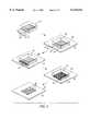
- FIG. 1illustrates schematically a technique for forming a high-carbon solid structure against a surface using a mold, from a fluid precursor
- FIG. 2is a schematic illustration of a technique for transferring a fluid precursor of a high-carbon solid structure from indentations in a mold to a substrate surface, forming high-carbon solid structures at the surface, and removing free-standing articles from the surface;
- FIG. 3is a photocopy of a scanning electron micrograph (SEM) image of a free-standing high-carbon structure
- FIG. 4is a photocopy of an SEM image of a free-standing, high-carbon structure
- FIG. 5is a photocopy of a scanning electron micrograph (SEM) image of a interdigitated electrode array formed of free-standing, high-carbon structures;
- FIG. 6is a photocopy of an SEM image of a high-carbon structure
- FIG. 7is a photocopy of an SEM image of a high-carbon grid structure
- FIG. 8is a photocopy of an SEM image of a crosslinked precursor of a high-carbon array, on a substrate, prior to carbonization;
- FIG. 9is a photocopy of an SEM image of a fracture plane of the article of FIG. 8, following carbonization
- FIG. 10is a photocopy of an SEM image of a high-carbon tube
- FIG. 11is a photocopy of an SEM image of a high-carbon pyramidal structure
- FIG. 12is a photocopy of an atomic force microscopy (AFM) image of a pyramidal high-carbon structure
- FIG. 13is a photocopy of an SEM image of a prior art, copper, TEM grid
- FIG. 14is a photocopy of an SEM image of a high-carbon TEM grid
- FIG. 15is a schematic illustration of an electrically-induced high-carbon microstructure deflection device.
- FIG. 16is a plot of angular deflection of an electrostatically-actuated central plate of a high carbon structure of FIG. 3 as a function of voltage applied to nearby, spaced electrodes.
- the present inventionprovides techniques for forming high-carbon solid articles from precursors of these articles, using molds, and articles produced according to the techniques.
- a variety of articles useful in microanalytical, microelectrical, micromechanical, and medical and biomedical fieldscan be produced according to the techniques.
- the high-carbon structures of the inventionfor example glassy carbon structures, can be used in lieu of silicon in applications where light weight, high chemical resistance to strong bases, or thermal stability are required properties.
- the lower Young's modulus of glassy carbon (10-40 GPa) compared to that of silicon (190 GPa for monocrystalline silicon, 40-170 GPa for polysilicon)can be an advantage in applications where the brittleness of silicon is a limiting factor, or where the extreme stiffness of silicon is a disadvantage (for example, in electrostatically driven actuators).
- silicon surfaceshave a high surface energy since they are covered with a 10-20 A thick native oxide layer. Surfaces with high free energies will be subjected to capillary forces when in close proximity.
- Stictionthat is, the adhesion between two surfaces, depends on van der Waals, electrostatic, and capillary forces. The contribution of capillarity accounts for most of the forces responsible for stiction. Stiction often limits the performance of microelectromechanical systems: once two surfaces are in contact, only a restoring force can separate them.
- the density of oxygen-containing, polar surface functional groupsis lower on carbon than on Si/SiO2.
- the ability to functionalize the surface of oxidized carbon further to introduce hydrocarbon or fluorocarbon groupsoffers a route to materials with very low surface free energies and low potential for stiction.
- the relatively rough surface of carbon solidsmay also prevent stiction since the true area of contact between rough surfaces is smaller than between smoother surfaces.
- the inventionutilizes an applicator having an indentation pattern that can be used to transfer a fluid precursor of a high-carbon structure from the indentations to a substrate surface or that can serve as a mold that when, positioned proximate a substrate surface, can define a region in which the fluid precursor is positioned.
- the substratecan be another applicator.
- FIG. 1illustrates schematically a technique for forming a high-carbon structure at a substrate surface.
- Article 20also can define a forming article or micromold placed proximate the substrate surface and used to guide a fluid precursor of a high-carbon structure so as to position the precursor in a pattern at a predetermined region or regions proximate the substrate surface.
- proximateis meant to define at a substrate surface, that is, in contact with a substrate surface, or at a position near a substrate surface and fixed relative to the substrate surface.
- a substrate surfacecarries an adhesion promoter, for example a self-assembled monolayer
- activity at the surface of the self-assembled monolayer or adhesion promoteris intended to mean activity proximate the substrate surface.
- a fluid precursor 36 of a high-carbon structureis placed adjacent one or more openings of channels 32 and introduced into the channels and allowed to flow adjacent portions 34 of substrate surface 28 in register with indentations 24. Fluid precursor 36 can be urged to flow via, for example, pressure applied to the fluid as it is positioned so as to enter the channels, or vacuum created within the channels by, for example, connection of the outlets of the channels to a source of vacuum.
- the fluidcan be allowed to flow into the mold via capillary action.
- Capillary filling of the moldis especially useful when the mold is of very small dimension (in particular in the micro scale) and is defined herein to mean that when a fluid precursor is positioned adjacent an opening or channel 32 formed by a portion 34 of the substrate surface and an indentation 24 of article 20, the fluid precursor will flow into at least a portion of the channel spontaneously.
- the precursorcan be solidified, or carbonized, before or after removal of applicator 20 from substrate surface 28.
- the fluidis viscous enough, for example via having been crosslinked by gentle heating, the applicator can be removed and the precursor hardened at the surface without unacceptable loss of dimensional integrity.
- the pattern of parallel indentations 24 formed in surface 22 of micromold 20is for illustrative purposes only. Any pattern, for example a pattern defined by a single indentation or many indentations, one or more of the indentations defining a non-linear pathway of uniform or non-uniform depth, is intended to fall within the scope of the invention. Various patterns are illustrated in subsequent figures.
- the indentation patterncan be of a variety of dimensions and, according to one aspect of the invention, includes a region having a dimension of less than 2 millimeters.
- the dimensioncan be a lateral dimension or vertical dimension.
- “Lateral dimension”is meant to define a dimension parallel to application surface 22.
- Very dimensionis meant to define a dimension perpendicular to the surface.
- a lateral or vertical dimensioncan be a dimension of a feature that is a portion of an overall structure. That is, an overall structure could have a width of 5 millimeters parallel to the surface and a height of 5 millimeters relative to the surface, but include a ridge on the top of the structure of 0.5 millimeter height and 0.5 millimeter width. That sub-feature would, by definition, have a lateral dimension of 0.5 millimeter and a vertical dimension of 0.5 millimeter.
- the indentation patternincludes a portion having a dimension of less than about 1 mm, preferably less than about 500 microns or less than about 100 microns, more preferably less than about 50, 20, or 10 microns, and more preferably still less than about 5 microns.
- an indentation pattern having a portion including a dimension on the order of 1 micronis provided.
- the dimension of the indentationscan be altered by deforming article 20, as described in co-pending, commonly-owned U.S. patent application Ser. No. 08/397,635, filed Mar. 1, 1995 by Whitesides, et al., entitled “Microcontact Printing on Surfaces and Derivative Articles", incorporated herein by reference.
- high-carbon article or articles 38 resulting from the techniquecan have lateral dimensional features that correspond to the lateral dimensional features of indentations 32 of the micromold.
- the fluid precursorneed not completely fill channels 32, and this is preferred according to embodiments in which the lateral dimension of high-carbon article 38 formed from the fluid precursor is to be minimized.
- fluid precursor 36is introduced into channels 32 in an amount small enough that the fluid precursor wets only the corners of the channels.
- the precursorwhen a fluid precursor, substrate, and micromold are selected such that the fluid precursor will wet the micromold efficiently via capillary action, when a small amount of fluid precursor is supplied to the mold channel or channels, the precursor will selectively wet portions of the channels having an interior angle relatively low relative to the rest of the channel (such as corners 39 defined by the abutment of contact surface 26 against substrate surface 28 at the edge of region 34 of the substrate surface).
- the fluid precursorwets the corners selectively and the precursor is carbonized to form a high-carbon structure, the resulting structure can define a pattern having a dimension smaller than that of the lateral dimension of indentation 24.
- the lateral dimension of structure 38is narrower than the narrowest lateral dimension of channel 24 of the micromold, and can have a height significantly less than the height of the channel.
- the lateral dimension of high-carbon article 38 according to this embodimentcan be on the order of less than or equal to about 100 microns or 50 microns, or preferably less than about 20 or 10 microns, more preferably less than about 5 microns or 1 micron, and according to a particularly preferred embodiment less than approximately 0.2 micron.
- substrate 30 of the inventioncan be of the same material as the bulk material of substrate 30, or a different material.
- Substrates exposing a variety of functional surfacessuch as hydrophobic, hydrophilic, and biologically compatible or non-compatible surfaces are known, and are suitable for use with the invention.
- Substrates that are somewhat fluidare known as well, and are acceptable for use in the invention to the extent that a useful pattern can be formed thereupon.
- free-standing high-carbon structuresare formed, and in these embodiments, it has been found that a substrate having a chromium surface against which a high-carbon structure is formed is most useful.
- a silicon wafer carrying a chromium filmis particularly useful.
- Article 20similarly can be formed of a variety of materials.
- substrate surface 28 and/or contact surface 26 of article 20is an elastomer or other conformable material.
- contact surface 26 and more preferably, for ease of fabrication, the entire article 20,is formed of an elastomer, most preferably polydimethyl siloxane.
- an elastomerdefines substrate surface 28 or contact surface 26, or preferably micromold 20, an optimal seal is created between contact surface 26 and portions of substrate surface 28 adjacent and contiguous with portions 34 that with indentations 24 define channels 32. This results in optimal confinement of fluid precursor 36 to channels 32.
- pressurecan be applied to micromold 20 against substrate 30 during micromolding, but according to embodiments in which an elastomer is used as described, pressure need not be applied as the elastomer conforms well to the surface against which it mates thus sealing channels 32.
- the micromold 20can be fabricated of an elastomer in a manner analogous to the fabrication of a stamp from an elastomer as described in co-pending, commonly-owned U.S. application Ser. No. 08/131,841 by Kumar, et al, entitled “Formation of Microstamped Patterns on Surfaces and Derivative Articles", filed Oct. 4, 1993, and incorporated herein by reference.
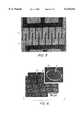
- FIG. 2illustrates another embodiment of the invention in which, rather than forming high-carbon structures via micromolding, a microtransfer molding technique is used to transfer a set of patterns, in parallel, to a substrate surface (parallel molding of a variety of similar patterns via micromolding as illustrated in FIG. 1 is embraced by the invention as well).
- a transfer article 40which can be made of the same material from which article 20 is made, includes a plurality of indentation patterns 42 that can be identical.
- Application of the fluid precursor 36 to the plurality of indentation patterns 42, followed by positioning the indentation patterns of the applicator adjacent the substrate surfaceresults in transfer of the fluid precursor, in the pattern, to the substrate surface.
- Carbonizationcan take place prior to or after removal of the article from the substrate surface, preferably after removal of the article following brief, mild heating.
- carbonizationmeans treatment of a fluid precursor of a high-carbon structure to conditions, such as high temperature, that drives off any solvent and eliminates heteroatoms such as hydrogen, oxygen, and the like to a degree resulting in the percent carbon values listed herein. Greater degrees of carbonization can result in a greater carbon-to-hydrogen ration since higher conjugation is created. At higher conjugation, electrical conductivity increases.
- precursor 36is applied to indentation patterns 42 preferably by coating the entire surface 41 with precursor 36, spreading the precursor back and forth across surface 41 with an applicator to assure filling of each of indentations 42, and removal of excess precursor until a small drop of precursor is left essentially in the center of the indentation pattern.
- surface 41 of the applicatoris brought into contact with substrate surface 28 to transfer the fluid precursor, in the pattern, to the substrate surface.
- the substrate and applicatorare, together, heated gently to, for example, 150° C.
- high-carbon microstructures 46can be allowed to remain on the substrate surface, or can be removed from the substrate surface to define free-standing articles.
- the fluid precursor 36 of high-carbon articles 46is transferred essentially instantaneously to substrate surface 28, in indentation pattern 42.
- high-carbon solid structureis meant to define a structure having a final, structural carbon content of at least 40% carbon atoms based on the overall number of atoms present, preferably at least 50% carbon atoms, more preferably at least 75% carbon atoms, more preferably at least 80% carbon atoms, more preferably at least 90% carbon atoms, more preferably at least 95%, and more preferably still at least 98% carbon atoms that is obtained by carbonization (heating) of a fluid precursor that optionally can be carried in or dissolved in a fluid carrier or solvent.
- the definitionis meant to embrace non-fibrous, organized carbon structures meeting these limitations, excluding pure diamond or graphite.
- glassy carbonalso known as vitreous carbon
- vitreous carbonGlassy carbon is described in Carbon: Electrochemical and Physico-Chemical Properties, K. Kinoshita, Wiley and Sons (1988). Glassy carbon is often produced by carbonization of organic polymeric precursors such as resins of furfuryl alcohol, phenol formaldehyde, acetone-furfural, or furfuryl alcohol-phenol copolymers. Both electrically conducting and electrically non-conducting, solid and open structures can be prepared from commercially available precursor. The high-carbon solid structures typically are prepared by heat treatment at elevated temperatures (1000-3000° C.) of polymeric precursors.
- the high-carbon solid structures of the inventionpreferably are electrically conducting, impermeable to gases, and have a low coefficient of thermal expansion, having a density of about 1.3-1.5 grams per cubic centimeter, and a non-interconnected porous microstructure.
- the structuresare highly chemically stable (inert in strong acids and strong bases), and stable in air at temperatures up to 500° C.
- the structurestypically have a Young's modulus of about 10-40 GPa.
- An exemplary fluid precursor of the high-carbon solid structuresis a polymeric fluid sold under the trademark FurcarbTM by QO Chemicals, West Lafayette, Ind.
- a simple screening test for determining useful precursors of high-carbon materials of the inventioninvolves providing a known precursor and testing its viscosity to determine whether it can fill a mold having dimensions on the order of dimensions desired in a final high-carbon structure. If the material is too viscous, it can be determined whether viscosity can be lowered by dilution with a suitable solvent, preferably a low-boiling solvent that can be driven off via gentle heating prior to carbonization.
- FIG. 3is a photocopy of an SEM image of a free-standing, high-carbon solid structure 46, fabricated in accordance with the technique of FIG. 2.
- free-standingit is meant that the structure need not be supported by a substrate, and is not an integral part of a substrate.
- the structurehas a variety of different feature sizes, and includes a central portion 50 supported only by two torsion members 52. Central portion 50 can be used to deflect light, to register acceleration or electrical field, and the like as described below in accordance with a variety of techniques.
- FIG. 4is an SEM image of another free-standing, high-carbon solid structure in a pattern including very small feature dimensions.
- FIG. 5is a photocopy of a SEM image of an interdigitated electrode array including a plurality of electrodes 54 interdigitated among electrodes 56.
- the interdigitated electrodesmay desirably not be electrically connected.
- an electrical and structural connectionexists between electrodes 54 and electrodes 56 in FIG. 5, but this connection was subsequently broken to define a non-connected interdigitated array.
- FIG. 6is a photocopy of an SEM image (including inset) of a high-carbon solid structure 58 including a plurality of essentially circular holes 60.
- Article 58is a free-standing structure formed by molding a fluid precursor of the structure between a chromium-coated silicon substrate and an elastomeric mold having a plurality of circular protrusions corresponding to holes 60.
- Article 58is electrically conductive, and can be used as an electron-beam focusing apparatus or as one or more electrostatic lenses, in combination with a source of electrons.
- An arrangementcould involve a first electrode on a first side of article 58 and a second electrode of opposite charge on a second side of article 58, an electrostatic charge being provided between the electrodes for passage of electrons through holes 60, where they are focused, and direction of the electrons to a target.
- electrostaticswould recognize, on the basis of this disclosure, a range of suitable systems and applications.
- FIG. 7is a SEM image of a high-carbon solid structure formed by placing together two elastomeric molds having contoured surfaces defining a linear array of grooves, the molds offset from each other in terms of alignment of linear grooves, followed by gentle heating to crosslink, and then carbonization.
- FIG. 8is an SEM image, before carbonization, of a high-carbon solid structure 62 similar to structure 46, but with smaller bulk feature dimensions. Additionally, article 62 includes a top surface 64 that is patterned with a series of aligned indentations 66 and protrusions 68.
- FIG. 9is an SEM image of a fracture plane of the article of FIG. 8, following carbonization, showing the structure of protrusions 68.
- This "two-layer" structurecan be formed readily in accordance with the technique of the invention in a single molding step, followed by carbonization, wherein the prior art at least a two-step process typically would be required, a first step involving preparation of the bulk of article 62 without protrusions 68, and a separate step, with a separate mask, necessary for formation of ridges 68.
- Article 62can find use as a diffraction grating, and electrical or mechanical actuation of portions of article 62, as described below, facilitate use of the article as a sensor or other device.
- Protrusions 68 of article 62are approximately 1 micron in height, and the remainder of article 62 is approximately 20 microns in height.
- FIG. 10is a photocopy of an SEM image of a high-carbon solid tube formed by carbonizing a commercially-available glass capillary coated with polyimide (sold for the purpose of capillary electrophoresis), and dissolution of the capillary with a suitable etchant.
- FIG. 11is a photocopy of an SEM image of an essentially pyramidal high-carbon solid structure.
- the pyramidal structurewas formed using a technique involving casting an elastomeric mold against a surface of an anisotropically-etched silicon substrate.
- FIG. 12is an AFM image of a similarly-created essentially pyramidal high-carbon structural element.
- the feature size of the tip of the pyramidal structure of FIG. 12is on the order of 100 nm.
- FIGS. 13 and 14are photocopies of SEM images of a comparative, copper TEM grid and a high-carbon solid TEM grid of the invention, respectively.
- TEMtransmission electron microscopy
- a sampleis held by an electrically-conductive grid such as the commercially-available grid of FIG. 13, electrons are directed toward the sample, and an electron shadow image of the sample is recorded.
- the gridbe electrically-conductive so as to dissipate charge resulting from electron bombardment of the grid.
- metal gridssuch as the prior art grid of FIG. 13 cannot withstand certain corrosive environments.
- the grid of the invention(FIG. 14) facilitates recovery of a sample from a very corrosive bath and exposure of the sample to TEM conditions.
- the high-carbon solid TEM grids of the inventionare a significant improvement over prior art grids not only because of the corrosion resistance described above, but because much smaller grids (higher mesh size) can be prepared in accordance with the invention than are known in the art for carbon grids.
- TEM carbon gridsare known, but typically have a relatively course mesh of less than 100 (100 mesh is 100 grid bars per inch).
- Carbon TEM grids of the inventionare provided of at least 100 mesh, preferably at least 250 mesh, more preferably at least 300 mesh, more preferably still at least 400 mesh, more preferably still at least 500 mesh, and in a particularly preferred embodiment, high-carbon TEM grids of at least or greater than 600 mesh, are provided.
- Diamond TEM gridsare manufactured by GMMT Ltd., UK, including 1 millimeter hole, 2 ⁇ 1 slot and 200 mesh high transmission grids, commercially available through SPI supplies. 75 mesh carbon composite grids are commercially available, manufactured by Agar Scientific, UK.
- the technique of the inventioncan be carried out on nonplanar, for example, curved surfaces when a flexible or elastomeric applicator (20/40) is used.
- a nonplanar substrate 28exists, a flexible or elastomeric applicator 20 or 40 can be bent to conform to the nonplanar substrate surface and the technique carried out as described.
- a precursor 36 of a high-carbon solid structureis viscous enough, a nonplanar substrate, such a cylindrical article (capillary or the like) can be rolled across surface 41 or 22 of applicator 40 or 20, respectively, the pattern transferred to the nonplanar article, and the high-carbon structure carbonized on the surface of the article.
- the small, high-carbon solid structures of the inventionfind a variety of uses. For example, electrostatic lenses (for focusing electron beams; see FIG. 6), cantilevered structures, interdigitated comb structures for use as sensors, accelerometers, pressure sensors, and actuators, suspended micromirrors (light beam redirection uses), suspended vibrating structures (accelerometers, pressure sensors) and other types of motion sensors, suspended structures with diffraction gratings (beam splitting and redirection which are basic units for color displays), implantable devices such as physiological electrodes, microanalytical components (e.g., tips for scanning, tunneling microscopes; see FIGS.
- high-carbon materialscan be tailored in terms of electronic properties by subjecting the materials to a selected thermal treatment.
- certain high-carbon precursor materialscan be treated in one way to create a high-electrical resistance carbon structure, and in another way to create an electrically-conductive carbon structure.
- an electronic circuitcan be fabricated by forming a structure in the shape of a circuit, and treating different portions of the circuit with different carbonization treatment temperatures (for example via laser heating) to create different areas of different electrical character.
- resistors, capacitors, and the likecan be formed in a single electrical circuit using the molding technique of the invention.
- various properties of various high-carbon structurescan be tailored using fillers such as ceramics, silica, nanotubes, carbon black, and the like. These additives can be used to change mechanical properties.
- a high-carbon structure of desired shapeis created by etching.
- a high-carbon structureis provided, and a portion of the structure is etched by exposure to a chemical species with which the high-carbon structure is reactive.
- a thin film of high-carbon structural materialcan be fabricated on a substrate and exposed, in a predetermined pattern, to reactive ion etching conditions (oxygen plasma, CF 4 plasma, or the like).
- the predetermined patterncan be defined by a mask of any type, including a mask applied via microcontact printing as described in U.S. Pat. No. 5,512,131 and in International Patent Publication No. WO 96/29629, filed Mar. 1, 1996, both documents incorporated herein by reference.
- Reactive ion etchingis beneficial since it is compatible with the silicon microfabrication industry.
- Etchingcan take place before or after carbonization of the high-carbon structure precursor, and after carbonization a high-carbon structure such as a glassy carbon structure can be created.
- PDMSpolydimethyl siloxane
- the PDMS moldswere prepared by casting PDMS (Sylgard 184, Dow Coming) on photolithographically generated masters consisting of patterned films of photoresist (Microposit STR 1075, Shipley, Mass.).
- the masks used in the photolithographic stepwere prepared by rapid prototyping.
- a computer file of the design of interestwas generated using Freehand 5.5. The file was printed on a transparent film with a high resolution printer (resolution>3300 dpi), and that transparent film was used as a mask to generate surface relief patterns in films of photoresists coated on Si wafers.
- the substrates used for the preparation of the microstructures and subsequent carbonizationwere obtained by electron-beam evaporation of chromium thin films (400 ⁇ ) onto silicon wafers.
- Furfuryl alcohol modified phenolic resinwas obtained from Q.O. Chemicals (Furcarb LP-520). Curing of the latter resin required the addition of a latent, heat-activated catalyst such as a 50% aqueous solution of ZnCl 2 . The amount of catalyst never exceeded 10% (w/w) of the resin in order to prevent a too rapid cure and potential deformation of the microstructures.
- CAUTIONMixing an acid catalyst with furfuryl alcohol-based resins induces an exothermic reaction. Alternatively, Bakelite (Georgia Pacific) was used, which does not require addition of a catalyst.
- the precursor selectedwas a furfuryl alcohol-modified phenolic resin (alternatively, Bakelite (Georgia Pacific) can be used.
- This type of polymeris widely used as a precursor to carbon solids because of its low cost and relatively high carbon yield ( ⁇ 50%).
- Patterns of that polymerwere generated, according to one set of embodiments, by allowing the fluid precursor to spontaneously fill the capillary channels defined by a surface relief of the PDMS mold in conformal contact with a substrate. This technique was used to prepare continuous structures such as wires and grids (e.g. structures shown in FIGS. 6 and 7).
- the liquid polymerwas applied to the recessed pattern of the PDMS mold.
- the excess polymerwas removed by gently scraping with the edge of a second piece of PDMS.
- the PDMS moldwas placed in contact with the substrate; this contact constrained the remaining polymer in the recessed channels of the mold.
- An excessive quantity of polymerprevented conformal contact of the PDMS mold with the substrate, so the quantity of polymer applied to the mold was minimized.
- the liquid polymerwas cured within the mold by placing the substrate on a hot plate. The temperature was increased slowly from ⁇ 80 to 150° C. over ⁇ 45-60 min in order to induce polymerization of the liquid polymers. A fast cure distorted or destroyed the structure. Prolonged contact between the PDMS mold and the polymer was also detrimental, as the cured polymer tended to remain trapped in the mold rather than being transferred to the substrate. The best results were achieved when the procedure was performed in less than 1.5 h.
- the PDMS moldwas removed, and the supported polymeric structures were converted into free-standing high-carbon structures by carbonization (400-1000° C.; in other processes, temperatures of 1800° C. were reached, and temperatures up to 3000 are expected to be potentially useful) under an inert atmosphere (argon).
- carbonizationwas performed in a Blue M/Lindberg MiniMite tube furnace fitted with a quartz tube. The samples were placed in an alumina boat and introduced in the quartz tube. The chamber was deoxygenated by a rapid flow of argon for ⁇ 20 min prior to carbonization. Carbonization was performed under a positive pressure of argon. The temperature increased at a rate of 5° C./min up to the final temperature. The samples were kept at the final temperature for 10 min, and then allowed to cool down to room temperature.
- Resistance measurementswere performed with a hand-held voltmeter.
- the density of sampleswas estimated by floating solid samples in liquids of known densities.
- SEMwas performed on a JEOL JSM-6400 scanning electron microscope operated at 15 keV.
- the sampleswere either glued to conductive carbon tape, or glued to a silicon substrate with silver paint.
- X-ray photoelectron spectrawere obtained on a SSX-100 spectrometer (Surface Science Laboratories) using a monochromatic Al Ka X-ray source.
- the spot sizewas -1 mm 2 with an analyzer pass energy of 150 eV.
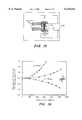
- a Free-standing, high-carbon microstructure as shown in FIG. 3was mounted on a substrate as illustrated in FIG. 15.
- the structure 78was glued with conductive silver paint 76 over the edges of two cover slips 72 separated by ⁇ 1 mm.
- the resistivity of the carbon solidwas ⁇ 0.03 ⁇ .cm.
- the central plate 79 of the devicewas electrostatically actuated simultaneously by attractive and repulsive forces: a voltage was applied between the carbon structure and one of two underlying silver electrodes 80 above which the plate 79 was suspended (attractive), while the second silver electrode was held at the same potential as the carbon structure (repulsive).
- the platewas deflected, and angle of deflection of a light beam directed toward the structure was thereby controlled electrostatically.
- the angular deflection of the central plate as a function of applied voltagewas plotted (FIG. 16), and showed smooth transition dependant on several factors including applied voltage, distance between the moving carbon element of the microstructure and the counter electrodes, and spring constant of the microstructure.
- the distance between the carbon microstructure and the counter electrodeswas determined by the thickness of the insulating layer (glass cover slips or polyimide films) used in the procedure. As the thickness of that layer decreased, so did the voltage required to actuate the central plate.
- the structural dimensions and mechanical properties of the carbonaceous soliddefine the spring constant of the structure.
- the mechanical properties of the materialwere primarily defined by the temperature of pyrolysis. Design can enable deflection to be optimized by control of thickness, width, and dimensions of the supporting arms.
- the mechanical, electrical, and chemical properties of high-carbon solidscan be controlled over wide ranges by the temperature at which these solids are prepared. (see Jenkins, et al. Polymeric Carbons--Carbon Fibre, Glass and Char; Ed: Cambridge University Press, Cambridge 1976; Spain, Chemistry and Physics of Carbon; (Ed: Walker Jr., P. L.; Thrower, P. A.), Marcel Dekker. Inc., New York, vol. 16, 1981, pp. 119-304).
- the range of electrical properties that can be achievedis especially interesting: the conductivity of a phenol-formaldehyde resin can be controlled over a range of ⁇ 10 19 ⁇ -1 cm -1 by pyrolysis.
- Supported structures of a phenol-formaldehyde resin and of a furfuryl alcohol modified phenolic resinwere prepared by the technique illustrated in FIG. 1, using a PDMS mold.
- the PDMS moldwas placed on a substrate, as described; the pattern in the PDMS formed a network of channels.
- a drop of fluid polymer precursorwas placed at one end of the channels, and the fluid filled the channels by capillary action.
- the substratewas placed on a hot plate and the polymer slowly cured (from 90 to 150° C.) for 1 hr.
- the PDMS stampwas then removed from the substrate.
- the structure defined by the surface relief in the PDMSremained on the substrate.
- After carbonization at 1000° C.the resulting structure was high-carbon wires ⁇ 7 mm long, 40 mm wide, 6 mm thick, and were separated by 60 mm.
- the wiresunderwent shrinkage of ⁇ 20% on carbonization.
- the resistivity of wires prepared by carbonization between 600-1000° C.was determined by applying patches of silver paint to both ends of an array of 8-12 of the wires and multiplying the overall resistance by the number of wires electrically connected.
- the room temperature resistivity of the carbonaceous solid as a function of the maximum temperature reached during heat treatmentwas plotted. The resistivity dropped sharply at temperatures >600° C., from ⁇ 10 3 ⁇ .cm to reach a plateau of about ⁇ 10 -2 ⁇ .cm at ⁇ 1000° C.
- the density of high-carbon solidswas tailored. It was found that the density increased from 1.20 to 1.51 g/cm 3 in the range of temperature investigated (400-1000° C.).
- the density of a pyrolyzed phenol-formaldehyde resinreached a minimum ( ⁇ 1.1-1.2 g/cm 3 ) at -400-500° C., then increases to -1.5 g/cm 3 at 1200° C.
- the density of graphiteis 2.25 g/cm 3
- that of diamondis 3.51 g/cm 3 .
Landscapes
- Chemical & Material Sciences (AREA)
- Engineering & Computer Science (AREA)
- Nanotechnology (AREA)
- Ceramic Engineering (AREA)
- Manufacturing & Machinery (AREA)
- Materials Engineering (AREA)
- Crystallography & Structural Chemistry (AREA)
- Organic Chemistry (AREA)
- Structural Engineering (AREA)
- Health & Medical Sciences (AREA)
- Life Sciences & Earth Sciences (AREA)
- General Health & Medical Sciences (AREA)
- Molecular Biology (AREA)
- Inorganic Chemistry (AREA)
- Physics & Mathematics (AREA)
- Composite Materials (AREA)
- Condensed Matter Physics & Semiconductors (AREA)
- General Physics & Mathematics (AREA)
- Carbon And Carbon Compounds (AREA)
Abstract
Description
Claims (19)
Priority Applications (3)
| Application Number | Priority Date | Filing Date | Title |
|---|---|---|---|
| US08/797,165US6143412A (en) | 1997-02-10 | 1997-02-10 | Fabrication of carbon microstructures |
| AU66530/98AAU6653098A (en) | 1997-02-10 | 1998-02-10 | Fabrication of carbon microstructures |
| PCT/US1998/002573WO1998034886A1 (en) | 1997-02-10 | 1998-02-10 | Fabrication of carbon microstructures |
Applications Claiming Priority (1)
| Application Number | Priority Date | Filing Date | Title |
|---|---|---|---|
| US08/797,165US6143412A (en) | 1997-02-10 | 1997-02-10 | Fabrication of carbon microstructures |
Publications (1)
| Publication Number | Publication Date |
|---|---|
| US6143412Atrue US6143412A (en) | 2000-11-07 |
Family
ID=25170093
Family Applications (1)
| Application Number | Title | Priority Date | Filing Date |
|---|---|---|---|
| US08/797,165Expired - LifetimeUS6143412A (en) | 1997-02-10 | 1997-02-10 | Fabrication of carbon microstructures |
Country Status (3)
| Country | Link |
|---|---|
| US (1) | US6143412A (en) |
| AU (1) | AU6653098A (en) |
| WO (1) | WO1998034886A1 (en) |
Cited By (83)
| Publication number | Priority date | Publication date | Assignee | Title |
|---|---|---|---|---|
| US20020015993A1 (en)* | 1999-12-15 | 2002-02-07 | John Havens R. | Permeation layer attachment chemistry and method |
| US6359383B1 (en)* | 1999-08-19 | 2002-03-19 | Industrial Technology Research Institute | Field emission display device equipped with nanotube emitters and method for fabricating |
| US20020048833A1 (en)* | 2000-09-20 | 2002-04-25 | Eiichi Fujii | Manufacturing method and manufacturing device of microstructure |
| US20020076575A1 (en)* | 2000-09-18 | 2002-06-20 | Hong Yang | Fabrication of ceramic microstructures |
| US20020085954A1 (en)* | 1993-11-01 | 2002-07-04 | Nanogen, Inc. | Inorganic permeation layer for micro-electric device |
| US6420092B1 (en)* | 1999-07-14 | 2002-07-16 | Cheng-Jer Yang | Low dielectric constant nanotube |
| US20020113334A1 (en)* | 1996-09-25 | 2002-08-22 | Asahi Kasei Kabushiki Kaisha | Replica molding |
| US6488872B1 (en)* | 1999-07-23 | 2002-12-03 | The Board Of Trustees Of The University Of Illinois | Microfabricated devices and method of manufacturing the same |
| US6524517B1 (en)* | 1999-12-15 | 2003-02-25 | Nanogen, Inc. | Methods for molding and grafting highly uniform polymer layers onto electronic microchips |
| US6602567B2 (en)* | 1999-09-22 | 2003-08-05 | Chien-Chung Han | Micrometer-sized carbon tubes |
| US20030146145A1 (en)* | 2001-12-10 | 2003-08-07 | Jainamma Krotz | Mesoporous permeation layers for use on active electronic matrix devices |
| US20030170480A1 (en)* | 2002-01-18 | 2003-09-11 | North Carolina State University | Gradient fabrication to direct transport on a surface |
| US20030186405A1 (en)* | 2002-04-01 | 2003-10-02 | The Ohio State University Research Foundation | Micro/nano-embossing process and useful applications thereof |
| US20030203271A1 (en)* | 2002-04-24 | 2003-10-30 | The Regents Of The University Of California | Microfluidic fuel cell systems with embedded materials and structures and method thereof |
| US6655575B2 (en)* | 2002-04-16 | 2003-12-02 | The Curators Of University Of Missouri | Superplastic forming of micro components |
| US20040007799A1 (en)* | 2002-07-11 | 2004-01-15 | Choi Byung Jin | Formation of discontinuous films during an imprint lithography process |
| US6696220B2 (en) | 2000-10-12 | 2004-02-24 | Board Of Regents, The University Of Texas System | Template for room temperature, low pressure micro-and nano-imprint lithography |
| US20040046271A1 (en)* | 2002-09-05 | 2004-03-11 | Watts Michael P.C. | Functional patterning material for imprint lithography processes |
| US20040058067A1 (en)* | 2002-09-19 | 2004-03-25 | Law Kam S. | Method and apparatus for metallization of large area substrates |
| US20040062965A1 (en)* | 2002-09-30 | 2004-04-01 | The Regents Of The University Of California | Bonded polyimide fuel cell package and method thereof |
| US20040065252A1 (en)* | 2002-10-04 | 2004-04-08 | Sreenivasan Sidlgata V. | Method of forming a layer on a substrate to facilitate fabrication of metrology standards |
| US6719915B2 (en) | 1999-03-11 | 2004-04-13 | Board Of Regents, The University Of Texas System | Step and flash imprint lithography |
| US20040115279A1 (en)* | 2002-09-06 | 2004-06-17 | The Ohio State University | Microfabrication of polymer microparticles |
| US20040209191A1 (en)* | 2001-06-01 | 2004-10-21 | Adolf Bernds | Method for producing conductive structures by means of printing technique, and active components produced therefrom for integrated circuits |
| US6873087B1 (en) | 1999-10-29 | 2005-03-29 | Board Of Regents, The University Of Texas System | High precision orientation alignment and gap control stages for imprint lithography processes |
| US20050075708A1 (en)* | 2002-11-26 | 2005-04-07 | O'brien Robert C. | Nanotube coatings for implantable electrodes |
| US6916584B2 (en) | 2002-08-01 | 2005-07-12 | Molecular Imprints, Inc. | Alignment methods for imprint lithography |
| US20050156353A1 (en)* | 2004-01-15 | 2005-07-21 | Watts Michael P. | Method to improve the flow rate of imprinting material |
| US6921615B2 (en) | 2000-07-16 | 2005-07-26 | Board Of Regents, The University Of Texas System | High-resolution overlay alignment methods for imprint lithography |
| US6929762B2 (en) | 2002-11-13 | 2005-08-16 | Molecular Imprints, Inc. | Method of reducing pattern distortions during imprint lithography processes |
| US6946780B2 (en)* | 2000-11-06 | 2005-09-20 | Mitsubishi Denki Kabushiki Kaisha | Carbon body, process for producing the carbon body, and electric field emission electron source using the carbon body |
| US20050214164A1 (en)* | 2003-10-27 | 2005-09-29 | Mitsubishi Pencil Co., Ltd. | Optical measurement substrate and fabrication method for the same |
| US6954275B2 (en) | 2000-08-01 | 2005-10-11 | Boards Of Regents, The University Of Texas System | Methods for high-precision gap and orientation sensing between a transparent template and substrate for imprint lithography |
| US6964793B2 (en) | 2002-05-16 | 2005-11-15 | Board Of Regents, The University Of Texas System | Method for fabricating nanoscale patterns in light curable compositions using an electric field |
| US6990870B2 (en) | 2002-12-12 | 2006-01-31 | Molecular Imprints, Inc. | System for determining characteristics of substrates employing fluid geometries |
| DE102004033424A1 (en)* | 2004-07-10 | 2006-02-02 | Ovd Kinegram Ag | Method of modifying a microstructure of an article |
| US20060051980A1 (en)* | 2003-10-17 | 2006-03-09 | Rigaku Corporation | Rotary current-collecting device and rotating anode X-ray tube |
| US20060068107A1 (en)* | 2004-09-30 | 2006-03-30 | The Regents Of The University Of California | Surface and composition enhancements to high aspect ratio C-MEMS |
| US7071088B2 (en) | 2002-08-23 | 2006-07-04 | Molecular Imprints, Inc. | Method for fabricating bulbous-shaped vias |
| US7077992B2 (en) | 2002-07-11 | 2006-07-18 | Molecular Imprints, Inc. | Step and repeat imprint lithography processes |
| US7090716B2 (en) | 2003-10-02 | 2006-08-15 | Molecular Imprints, Inc. | Single phase fluid imprint lithography method |
| US7122079B2 (en) | 2004-02-27 | 2006-10-17 | Molecular Imprints, Inc. | Composition for an etching mask comprising a silicon-containing material |
| US7136150B2 (en) | 2003-09-25 | 2006-11-14 | Molecular Imprints, Inc. | Imprint lithography template having opaque alignment marks |
| US20060263460A1 (en)* | 2005-05-18 | 2006-11-23 | Chief Lin | Jig structure for manufacturing an image sensor |
| US7157036B2 (en) | 2003-06-17 | 2007-01-02 | Molecular Imprints, Inc | Method to reduce adhesion between a conformable region and a pattern of a mold |
| US20070000507A1 (en)* | 2005-06-29 | 2007-01-04 | Philip Morris Usa Inc. | Templated carbon fibers and their application |
| US20070026526A1 (en)* | 2005-03-31 | 2007-02-01 | Miyuki Takenaka | Method for quantitative analysis of metal element contained in resin material |
| US7179396B2 (en) | 2003-03-25 | 2007-02-20 | Molecular Imprints, Inc. | Positive tone bi-layer imprint lithography method |
| US20070138676A1 (en)* | 2005-12-15 | 2007-06-21 | Kabushiki Kaisha Kobe Seiko Sho (Kobe Steel, Ltd.) | Methods for producing glasslike carbon |
| US20080069962A1 (en)* | 2006-08-31 | 2008-03-20 | Light James P Ii | Compositions and Methods for Preserving Permeation Layers for Use on Active Electronic Matrix Devices |
| US20080103064A1 (en)* | 2006-06-13 | 2008-05-01 | Antara Biosciences Inc. | Microscale fluidic devices for electrochemical detection of biological molecules |
| US7396475B2 (en) | 2003-04-25 | 2008-07-08 | Molecular Imprints, Inc. | Method of forming stepped structures employing imprint lithography |
| US7452574B2 (en) | 2003-02-27 | 2008-11-18 | Molecular Imprints, Inc. | Method to reduce adhesion between a polymerizable layer and a substrate employing a fluorine-containing layer |
| US20090032741A1 (en)* | 2007-07-25 | 2009-02-05 | Nanocomp Technologies, Inc. | Systems and Methods for Controlling Chirality of Nanotubes |
| US20090047513A1 (en)* | 2007-02-27 | 2009-02-19 | Nanocomp Technologies, Inc. | Materials for Thermal Protection and Methods of Manufacturing Same |
| US20090069198A1 (en)* | 1999-09-30 | 2009-03-12 | Havens John R | Biomolecular Attachment Sites on Microelectronic Arrays and Methods Thereof |
| US20090215344A1 (en)* | 2005-07-28 | 2009-08-27 | Nanocomp Technologies, Inc. | Systems And Methods For Formation And Harvesting of Nanofibrous Materials |
| US20100000754A1 (en)* | 2008-05-07 | 2010-01-07 | Nanocomp Technologies, Inc. | Carbon nanotube-based coaxial electrical cables and wiring harness |
| US20100064973A1 (en)* | 2005-03-18 | 2010-03-18 | Tsinghua University | Apparatus and method for making carbon nanotube array |
| US20100104849A1 (en)* | 2005-05-03 | 2010-04-29 | Lashmore David S | Carbon composite materials and methods of manufacturing same |
| EP2219027A1 (en) | 2009-02-12 | 2010-08-18 | Centre National de la Recherche Scientifique | Devices and methods for observing the cell division |
| US20110005808A1 (en)* | 2009-07-10 | 2011-01-13 | Nanocomp Technologies, Inc. | Hybrid Conductors and Method of Making Same |
| US7906180B2 (en) | 2004-02-27 | 2011-03-15 | Molecular Imprints, Inc. | Composition for an etching mask comprising a silicon-containing material |
| US20110214850A1 (en)* | 2005-05-26 | 2011-09-08 | Nanocomp Technologies, Inc. | Nanotube Materials for Thermal Management of Electronic Components |
| US8016277B2 (en) | 2000-08-21 | 2011-09-13 | Board Of Regents, The University Of Texas System | Flexure based macro motion translation stage |
| US20110253907A1 (en)* | 2010-04-14 | 2011-10-20 | Beijing Funate Innovation Technology Co., Ltd. | Transmission electron microscope micro-grid |
| US8076386B2 (en) | 2004-02-23 | 2011-12-13 | Molecular Imprints, Inc. | Materials for imprint lithography |
| US8211214B2 (en) | 2003-10-02 | 2012-07-03 | Molecular Imprints, Inc. | Single phase fluid imprint lithography method |
| US8246886B2 (en) | 2007-07-09 | 2012-08-21 | Nanocomp Technologies, Inc. | Chemically-assisted alignment of nanotubes within extensible structures |
| US8349241B2 (en) | 2002-10-04 | 2013-01-08 | Molecular Imprints, Inc. | Method to arrange features on a substrate to replicate features having minimal dimensional variability |
| WO2013144302A1 (en) | 2012-03-29 | 2013-10-03 | Centre National De La Recherche Scientifique | Methods for observing cells with cell wall or invertebrate embryos with oblong eggshell |
| US20140054743A1 (en)* | 2012-08-24 | 2014-02-27 | Newport Fab, Llc Dba Jazz Semiconductor | Isolated Through Silicon Vias in RF Technologies |
| US20150017479A1 (en)* | 2012-01-30 | 2015-01-15 | Chung-Ang University Industry-Academic Corporation Foundation | Production method for glassy carbon mold |
| US9061913B2 (en) | 2007-06-15 | 2015-06-23 | Nanocomp Technologies, Inc. | Injector apparatus and methods for production of nanostructures |
| US9198232B2 (en) | 2008-05-07 | 2015-11-24 | Nanocomp Technologies, Inc. | Nanostructure-based heating devices and methods of use |
| US9223202B2 (en) | 2000-07-17 | 2015-12-29 | Board Of Regents, The University Of Texas System | Method of automatic fluid dispensing for imprint lithography processes |
| US9236669B2 (en)* | 2007-08-07 | 2016-01-12 | Nanocomp Technologies, Inc. | Electrically and thermally non-metallic conductive nanostructure-based adapters |
| US9718691B2 (en) | 2013-06-17 | 2017-08-01 | Nanocomp Technologies, Inc. | Exfoliating-dispersing agents for nanotubes, bundles and fibers |
| US10581082B2 (en) | 2016-11-15 | 2020-03-03 | Nanocomp Technologies, Inc. | Systems and methods for making structures defined by CNT pulp networks |
| US11279836B2 (en) | 2017-01-09 | 2022-03-22 | Nanocomp Technologies, Inc. | Intumescent nanostructured materials and methods of manufacturing same |
| US11434581B2 (en) | 2015-02-03 | 2022-09-06 | Nanocomp Technologies, Inc. | Carbon nanotube structures and methods for production thereof |
| USD1070796S1 (en)* | 2021-10-15 | 2025-04-15 | Shin-Etsu Chemical Co., Ltd. | Stamp component for transferring microstructure |
| CN120177536A (en)* | 2025-03-20 | 2025-06-20 | 杭州阿童木科技有限公司 | A transmission micrograting for nondestructive electron microscopy characterization with atomic-level precision |
Citations (24)
| Publication number | Priority date | Publication date | Assignee | Title |
|---|---|---|---|---|
| US3932568A (en)* | 1973-06-26 | 1976-01-13 | Friction Products Inc. | High-energy brake and brake components |
| US4035265A (en)* | 1969-04-18 | 1977-07-12 | The Research Association Of British, Paint, Colour & Varnish Manufacturers | Paint compositions |
| US4137477A (en)* | 1975-05-28 | 1979-01-30 | U.S. Philips Corporation | Electrodes, for example grid-like electrodes for use in electron tubes, and a method for manufacturing same |
| US4466932A (en)* | 1981-12-30 | 1984-08-21 | Kanebo Ltd. | Process for producing carbon articles |
| US4612100A (en)* | 1983-12-20 | 1986-09-16 | Siemens Aktiengesellschaft | Method for the fabrication of an implantable electrode |
| US4706430A (en)* | 1985-12-26 | 1987-11-17 | Shimizu Construction Co., Ltd. | Concrete reinforcing unit |
| US4791037A (en)* | 1986-08-15 | 1988-12-13 | W. R. Grace & Co.-Conn. | Carbon electrode |
| US4804592A (en)* | 1987-10-16 | 1989-02-14 | The United States Of America As Represented By The United States Department Of Energy | Composite electrode for use in electrochemical cells |
| US4936956A (en)* | 1984-11-23 | 1990-06-26 | Massachusetts Institute Of Technology | Microelectrochemical devices based on inorganic redox active material and method for sensing |
| US5074313A (en)* | 1989-03-20 | 1991-12-24 | Cardiac Pacemakers, Inc. | Porous electrode with enhanced reactive surface |
| US5103837A (en)* | 1989-03-20 | 1992-04-14 | Siemens Aktiengesellschaft | Implantable stimulating electrode |
| US5110579A (en)* | 1989-09-14 | 1992-05-05 | General Electric Company | Transparent diamond films and method for making |
| US5118403A (en)* | 1989-06-09 | 1992-06-02 | The Research Foundation Of State Univ. Of N.Y. | Glassy carbon linear array electrode |
| US5147590A (en)* | 1990-05-02 | 1992-09-15 | Siemens Aktiengesellschaft | Method of making the electrode |
| US5236686A (en)* | 1991-08-19 | 1993-08-17 | University Of South Carolina | Precursor polyphenylene for and method of producing glassy carbon |
| EP0624558A2 (en)* | 1993-05-14 | 1994-11-17 | Hoechst Aktiengesellschaft | Method of making ceramic microstructures from polymer precursors |
| US5458632A (en)* | 1990-08-10 | 1995-10-17 | Pacesetter Ab | Implantable device and materials |
| US5503728A (en)* | 1992-09-09 | 1996-04-02 | Agency Of Industrial Science And Technology | Carbon sensor electrode and process for producing the same |
| US5512131A (en)* | 1993-10-04 | 1996-04-30 | President And Fellows Of Harvard College | Formation of microstamped patterns on surfaces and derivative articles |
| WO1996029629A2 (en)* | 1995-03-01 | 1996-09-26 | President And Fellows Of Harvard College | Microcontact printing on surfaces and derivative articles |
| US5578901A (en)* | 1994-02-14 | 1996-11-26 | E. I. Du Pont De Nemours And Company | Diamond fiber field emitters |
| US5584979A (en)* | 1994-05-27 | 1996-12-17 | Kone Instruments Oy | Ion-selective electrode and procedure for producing an ion-selective electrode |
| EP0629593B1 (en)* | 1993-06-14 | 1998-01-07 | Amoco Corporation | High modulus carbon and graphite articles and method for their preparation |
| US5776748A (en)* | 1993-10-04 | 1998-07-07 | President And Fellows Of Harvard College | Method of formation of microstamped patterns on plates for adhesion of cells and other biological materials, devices and uses therefor |
- 1997
- 1997-02-10USUS08/797,165patent/US6143412A/ennot_activeExpired - Lifetime
- 1998
- 1998-02-10WOPCT/US1998/002573patent/WO1998034886A1/enactiveApplication Filing
- 1998-02-10AUAU66530/98Apatent/AU6653098A/ennot_activeAbandoned
Patent Citations (25)
| Publication number | Priority date | Publication date | Assignee | Title |
|---|---|---|---|---|
| US4035265A (en)* | 1969-04-18 | 1977-07-12 | The Research Association Of British, Paint, Colour & Varnish Manufacturers | Paint compositions |
| US3932568A (en)* | 1973-06-26 | 1976-01-13 | Friction Products Inc. | High-energy brake and brake components |
| US4137477A (en)* | 1975-05-28 | 1979-01-30 | U.S. Philips Corporation | Electrodes, for example grid-like electrodes for use in electron tubes, and a method for manufacturing same |
| US4466932A (en)* | 1981-12-30 | 1984-08-21 | Kanebo Ltd. | Process for producing carbon articles |
| US4612100A (en)* | 1983-12-20 | 1986-09-16 | Siemens Aktiengesellschaft | Method for the fabrication of an implantable electrode |
| US4936956A (en)* | 1984-11-23 | 1990-06-26 | Massachusetts Institute Of Technology | Microelectrochemical devices based on inorganic redox active material and method for sensing |
| US4706430A (en)* | 1985-12-26 | 1987-11-17 | Shimizu Construction Co., Ltd. | Concrete reinforcing unit |
| US4791037A (en)* | 1986-08-15 | 1988-12-13 | W. R. Grace & Co.-Conn. | Carbon electrode |
| US4804592A (en)* | 1987-10-16 | 1989-02-14 | The United States Of America As Represented By The United States Department Of Energy | Composite electrode for use in electrochemical cells |
| US5074313A (en)* | 1989-03-20 | 1991-12-24 | Cardiac Pacemakers, Inc. | Porous electrode with enhanced reactive surface |
| US5103837A (en)* | 1989-03-20 | 1992-04-14 | Siemens Aktiengesellschaft | Implantable stimulating electrode |
| US5118403A (en)* | 1989-06-09 | 1992-06-02 | The Research Foundation Of State Univ. Of N.Y. | Glassy carbon linear array electrode |
| US5110579A (en)* | 1989-09-14 | 1992-05-05 | General Electric Company | Transparent diamond films and method for making |
| US5147590A (en)* | 1990-05-02 | 1992-09-15 | Siemens Aktiengesellschaft | Method of making the electrode |
| US5458632A (en)* | 1990-08-10 | 1995-10-17 | Pacesetter Ab | Implantable device and materials |
| US5236686A (en)* | 1991-08-19 | 1993-08-17 | University Of South Carolina | Precursor polyphenylene for and method of producing glassy carbon |
| US5503728A (en)* | 1992-09-09 | 1996-04-02 | Agency Of Industrial Science And Technology | Carbon sensor electrode and process for producing the same |
| US5698485A (en)* | 1993-05-14 | 1997-12-16 | Hoechst Aktiengesellschaft | Process for producing ceramic microstructures from polymeric precursors |
| EP0624558A2 (en)* | 1993-05-14 | 1994-11-17 | Hoechst Aktiengesellschaft | Method of making ceramic microstructures from polymer precursors |
| EP0629593B1 (en)* | 1993-06-14 | 1998-01-07 | Amoco Corporation | High modulus carbon and graphite articles and method for their preparation |
| US5512131A (en)* | 1993-10-04 | 1996-04-30 | President And Fellows Of Harvard College | Formation of microstamped patterns on surfaces and derivative articles |
| US5776748A (en)* | 1993-10-04 | 1998-07-07 | President And Fellows Of Harvard College | Method of formation of microstamped patterns on plates for adhesion of cells and other biological materials, devices and uses therefor |
| US5578901A (en)* | 1994-02-14 | 1996-11-26 | E. I. Du Pont De Nemours And Company | Diamond fiber field emitters |
| US5584979A (en)* | 1994-05-27 | 1996-12-17 | Kone Instruments Oy | Ion-selective electrode and procedure for producing an ion-selective electrode |
| WO1996029629A2 (en)* | 1995-03-01 | 1996-09-26 | President And Fellows Of Harvard College | Microcontact printing on surfaces and derivative articles |
Non-Patent Citations (12)
| Title |
|---|
| E. Kim et al., "Micromolding in Capillaries: Applications in Material Science", J. Am. Chem. Soc., vol. 118, No. 24, pp. 5722-5731, Jun. 1996. |
| E. Kim et al., "Polymer Microstructures Formed by Moulding in Capillaries", Natrure, vol. 376, No. 6541, pp. 581-584, Aug. 1985. |
| E. Kim et al., Micromolding in Capillaries: Applications in Material Science , J. Am. Chem. Soc., vol. 118, No. 24, pp. 5722 5731, Jun. 1996.* |
| E. Kim et al., Polymer Microstructures Formed by Moulding in Capillaries , Natrure, vol. 376, No. 6541, pp. 581 584, Aug. 1985.* |
| G. Leyendecker et al., "Laser Induced Chemical Vapor Deposition of Carbon", Appl. Phys. Lett., vol. 39, No. 11, pp. 921-923, Dec. 1981. |
| G. Leyendecker et al., Laser Induced Chemical Vapor Deposition of Carbon , Appl. Phys. Lett., vol. 39, No. 11, pp. 921 923, Dec. 1981.* |
| G. Savage, "Thermosetting Resin Matrix Precursors," Carbon-Carbon Composites, 1st Edition, Chapter 4, pp. 117-156, 1993. |
| G. Savage, Thermosetting Resin Matrix Precursors, Carbon Carbon Composites, 1st Edition, Chapter 4, pp. 117 156, 1993.* |
| O.J.A. Schueller, et al., "Fabrication of Glass Carbon Microstructures by Pyrolysis of Microfabricated Polymeric Precursors", Advanced Materials, vol. 9, No. 6, pp. 477-480 (May, 1997). |
| O.J.A. Schueller, et al., Fabrication of Glass Carbon Microstructures by Pyrolysis of Microfabricated Polymeric Precursors , Advanced Materials, vol. 9, No. 6, pp. 477 480 (May, 1997).* |
| T. M. Bloomstien et al., "Stereo Laser Micromachining of Silicon", Appl. Phys. Lett., vol. 61, No. 1, pp. 708-710, Jul. 1992. |
| T. M. Bloomstien et al., Stereo Laser Micromachining of Silicon , Appl. Phys. Lett., vol. 61, No. 1, pp. 708 710, Jul. 1992.* |
Cited By (130)
| Publication number | Priority date | Publication date | Assignee | Title |
|---|---|---|---|---|
| US20020085954A1 (en)* | 1993-11-01 | 2002-07-04 | Nanogen, Inc. | Inorganic permeation layer for micro-electric device |
| US7125236B2 (en)* | 1996-09-25 | 2006-10-24 | Shin - Etsu Chemical Co. Ltd. | Replica molding |
| US20020113334A1 (en)* | 1996-09-25 | 2002-08-22 | Asahi Kasei Kabushiki Kaisha | Replica molding |
| US6719915B2 (en) | 1999-03-11 | 2004-04-13 | Board Of Regents, The University Of Texas System | Step and flash imprint lithography |
| US6420092B1 (en)* | 1999-07-14 | 2002-07-16 | Cheng-Jer Yang | Low dielectric constant nanotube |
| US6488872B1 (en)* | 1999-07-23 | 2002-12-03 | The Board Of Trustees Of The University Of Illinois | Microfabricated devices and method of manufacturing the same |
| US6359383B1 (en)* | 1999-08-19 | 2002-03-19 | Industrial Technology Research Institute | Field emission display device equipped with nanotube emitters and method for fabricating |
| US6602567B2 (en)* | 1999-09-22 | 2003-08-05 | Chien-Chung Han | Micrometer-sized carbon tubes |
| US8288155B2 (en) | 1999-09-30 | 2012-10-16 | Gamida For Life B.V. | Biomolecular attachment sites on microelectronic arrays and methods thereof |
| US20090069198A1 (en)* | 1999-09-30 | 2009-03-12 | Havens John R | Biomolecular Attachment Sites on Microelectronic Arrays and Methods Thereof |
| US6873087B1 (en) | 1999-10-29 | 2005-03-29 | Board Of Regents, The University Of Texas System | High precision orientation alignment and gap control stages for imprint lithography processes |
| US6524517B1 (en)* | 1999-12-15 | 2003-02-25 | Nanogen, Inc. | Methods for molding and grafting highly uniform polymer layers onto electronic microchips |
| US20050158451A1 (en)* | 1999-12-15 | 2005-07-21 | Nanogen, Inc. | Permeation layer attachment chemistry and method |
| US6838053B2 (en) | 1999-12-15 | 2005-01-04 | Nanogen, Inc. | Platinum silicide permeation layer device with microlocaions |
| US20020015993A1 (en)* | 1999-12-15 | 2002-02-07 | John Havens R. | Permeation layer attachment chemistry and method |
| US6921615B2 (en) | 2000-07-16 | 2005-07-26 | Board Of Regents, The University Of Texas System | High-resolution overlay alignment methods for imprint lithography |
| US9223202B2 (en) | 2000-07-17 | 2015-12-29 | Board Of Regents, The University Of Texas System | Method of automatic fluid dispensing for imprint lithography processes |
| US6954275B2 (en) | 2000-08-01 | 2005-10-11 | Boards Of Regents, The University Of Texas System | Methods for high-precision gap and orientation sensing between a transparent template and substrate for imprint lithography |
| US8016277B2 (en) | 2000-08-21 | 2011-09-13 | Board Of Regents, The University Of Texas System | Flexure based macro motion translation stage |
| US7198747B2 (en) | 2000-09-18 | 2007-04-03 | President And Fellows Of Harvard College | Fabrication of ceramic microstructures |
| US20070142202A1 (en)* | 2000-09-18 | 2007-06-21 | President And Fellows Of Harvard College | Fabrication of ceramic microstructures |
| US20020076575A1 (en)* | 2000-09-18 | 2002-06-20 | Hong Yang | Fabrication of ceramic microstructures |
| US6645793B2 (en)* | 2000-09-20 | 2003-11-11 | Seiko Epson Corporation | Manufacturing method and manufacturing device of microstructure |
| US20020048833A1 (en)* | 2000-09-20 | 2002-04-25 | Eiichi Fujii | Manufacturing method and manufacturing device of microstructure |
| US6696220B2 (en) | 2000-10-12 | 2004-02-24 | Board Of Regents, The University Of Texas System | Template for room temperature, low pressure micro-and nano-imprint lithography |
| US6946780B2 (en)* | 2000-11-06 | 2005-09-20 | Mitsubishi Denki Kabushiki Kaisha | Carbon body, process for producing the carbon body, and electric field emission electron source using the carbon body |
| US20040209191A1 (en)* | 2001-06-01 | 2004-10-21 | Adolf Bernds | Method for producing conductive structures by means of printing technique, and active components produced therefrom for integrated circuits |
| US20050164283A1 (en)* | 2001-12-10 | 2005-07-28 | Nanogen, Inc. | Mesoporous permeation layers for use on active electronic matrix devices |
| US6960298B2 (en) | 2001-12-10 | 2005-11-01 | Nanogen, Inc. | Mesoporous permeation layers for use on active electronic matrix devices |
| US7597932B2 (en) | 2001-12-10 | 2009-10-06 | Nanogen, Inc. | Mesoporous permeation layers for use on active electronic matrix devices |
| US7270850B2 (en) | 2001-12-10 | 2007-09-18 | Nanogen, Inc. | Mesoporous permeation layers for use on active electronic matrix devices |
| US20030146145A1 (en)* | 2001-12-10 | 2003-08-07 | Jainamma Krotz | Mesoporous permeation layers for use on active electronic matrix devices |
| US8178163B2 (en) | 2002-01-18 | 2012-05-15 | North Carolina State University | Gradient fabrication to direct transport on a surface |
| US20060062921A1 (en)* | 2002-01-18 | 2006-03-23 | North Carolina State University | Gradient fabrication to direct transport on a surface |
| US20030170480A1 (en)* | 2002-01-18 | 2003-09-11 | North Carolina State University | Gradient fabrication to direct transport on a surface |
| US20100255194A1 (en)* | 2002-01-18 | 2010-10-07 | North Carolina State University | Gradient fabrication to direct transport on a surface |
| US6972155B2 (en) | 2002-01-18 | 2005-12-06 | North Carolina State University | Gradient fabrication to direct transport on a surface |
| US7601394B2 (en) | 2002-01-18 | 2009-10-13 | North Carolina State University | Gradient fabrication to direct transport on a surface |
| US20030186405A1 (en)* | 2002-04-01 | 2003-10-02 | The Ohio State University Research Foundation | Micro/nano-embossing process and useful applications thereof |
| US6655575B2 (en)* | 2002-04-16 | 2003-12-02 | The Curators Of University Of Missouri | Superplastic forming of micro components |
| US20030203271A1 (en)* | 2002-04-24 | 2003-10-30 | The Regents Of The University Of California | Microfluidic fuel cell systems with embedded materials and structures and method thereof |
| US6921603B2 (en) | 2002-04-24 | 2005-07-26 | The Regents Of The University Of California | Microfluidic fuel cell systems with embedded materials and structures and method thereof |
| US6964793B2 (en) | 2002-05-16 | 2005-11-15 | Board Of Regents, The University Of Texas System | Method for fabricating nanoscale patterns in light curable compositions using an electric field |
| US20040007799A1 (en)* | 2002-07-11 | 2004-01-15 | Choi Byung Jin | Formation of discontinuous films during an imprint lithography process |
| US6932934B2 (en) | 2002-07-11 | 2005-08-23 | Molecular Imprints, Inc. | Formation of discontinuous films during an imprint lithography process |
| US7077992B2 (en) | 2002-07-11 | 2006-07-18 | Molecular Imprints, Inc. | Step and repeat imprint lithography processes |
| US6916584B2 (en) | 2002-08-01 | 2005-07-12 | Molecular Imprints, Inc. | Alignment methods for imprint lithography |
| US7071088B2 (en) | 2002-08-23 | 2006-07-04 | Molecular Imprints, Inc. | Method for fabricating bulbous-shaped vias |
| US20040046271A1 (en)* | 2002-09-05 | 2004-03-11 | Watts Michael P.C. | Functional patterning material for imprint lithography processes |
| US6936194B2 (en) | 2002-09-05 | 2005-08-30 | Molecular Imprints, Inc. | Functional patterning material for imprint lithography processes |
| US20040115279A1 (en)* | 2002-09-06 | 2004-06-17 | The Ohio State University | Microfabrication of polymer microparticles |
| US20040058067A1 (en)* | 2002-09-19 | 2004-03-25 | Law Kam S. | Method and apparatus for metallization of large area substrates |
| US7029529B2 (en) | 2002-09-19 | 2006-04-18 | Applied Materials, Inc. | Method and apparatus for metallization of large area substrates |
| US20060000548A1 (en)* | 2002-09-30 | 2006-01-05 | The Regents Of The University Of California | Method of preparation of bonded polyimide fuel cell package |
| US7931993B2 (en)* | 2002-09-30 | 2011-04-26 | Lawrence Livermore National Security, Llc | Method of preparation of bonded polyimide fuel cell package |
| US20040062965A1 (en)* | 2002-09-30 | 2004-04-01 | The Regents Of The University Of California | Bonded polyimide fuel cell package and method thereof |
| US7732086B2 (en) | 2002-09-30 | 2010-06-08 | Lawrence Livermore National Security, Llc | Bonded polyimide fuel cell package |
| US20050255369A1 (en)* | 2002-09-30 | 2005-11-17 | The Regents Of The University Of California | Bonded polyimide fuel cell package |
| US6960403B2 (en) | 2002-09-30 | 2005-11-01 | The Regents Of The University Of California | Bonded polyimide fuel cell package and method thereof |
| US20040065252A1 (en)* | 2002-10-04 | 2004-04-08 | Sreenivasan Sidlgata V. | Method of forming a layer on a substrate to facilitate fabrication of metrology standards |
| US8349241B2 (en) | 2002-10-04 | 2013-01-08 | Molecular Imprints, Inc. | Method to arrange features on a substrate to replicate features having minimal dimensional variability |
| US6929762B2 (en) | 2002-11-13 | 2005-08-16 | Molecular Imprints, Inc. | Method of reducing pattern distortions during imprint lithography processes |
| US20050075708A1 (en)* | 2002-11-26 | 2005-04-07 | O'brien Robert C. | Nanotube coatings for implantable electrodes |
| US7162308B2 (en)* | 2002-11-26 | 2007-01-09 | Wilson Greatbatch Technologies, Inc. | Nanotube coatings for implantable electrodes |
| US6990870B2 (en) | 2002-12-12 | 2006-01-31 | Molecular Imprints, Inc. | System for determining characteristics of substrates employing fluid geometries |
| US7452574B2 (en) | 2003-02-27 | 2008-11-18 | Molecular Imprints, Inc. | Method to reduce adhesion between a polymerizable layer and a substrate employing a fluorine-containing layer |
| US7179396B2 (en) | 2003-03-25 | 2007-02-20 | Molecular Imprints, Inc. | Positive tone bi-layer imprint lithography method |
| US7396475B2 (en) | 2003-04-25 | 2008-07-08 | Molecular Imprints, Inc. | Method of forming stepped structures employing imprint lithography |
| US7157036B2 (en) | 2003-06-17 | 2007-01-02 | Molecular Imprints, Inc | Method to reduce adhesion between a conformable region and a pattern of a mold |
| US7136150B2 (en) | 2003-09-25 | 2006-11-14 | Molecular Imprints, Inc. | Imprint lithography template having opaque alignment marks |
| US8211214B2 (en) | 2003-10-02 | 2012-07-03 | Molecular Imprints, Inc. | Single phase fluid imprint lithography method |
| US7090716B2 (en) | 2003-10-02 | 2006-08-15 | Molecular Imprints, Inc. | Single phase fluid imprint lithography method |
| US20060051980A1 (en)* | 2003-10-17 | 2006-03-09 | Rigaku Corporation | Rotary current-collecting device and rotating anode X-ray tube |
| US20050214164A1 (en)* | 2003-10-27 | 2005-09-29 | Mitsubishi Pencil Co., Ltd. | Optical measurement substrate and fabrication method for the same |
| US7264756B2 (en)* | 2003-10-27 | 2007-09-04 | Mitsubishi Pencil Co., Ltd. | Optical measurement substrate and fabrication method for the same |
| US20050156353A1 (en)* | 2004-01-15 | 2005-07-21 | Watts Michael P. | Method to improve the flow rate of imprinting material |
| US8076386B2 (en) | 2004-02-23 | 2011-12-13 | Molecular Imprints, Inc. | Materials for imprint lithography |
| US7122079B2 (en) | 2004-02-27 | 2006-10-17 | Molecular Imprints, Inc. | Composition for an etching mask comprising a silicon-containing material |
| US7906180B2 (en) | 2004-02-27 | 2011-03-15 | Molecular Imprints, Inc. | Composition for an etching mask comprising a silicon-containing material |
| US20080088045A1 (en)* | 2004-07-10 | 2008-04-17 | Achim Hansen | Method for the Modification of a Microstructure of an Object |
| DE102004033424A1 (en)* | 2004-07-10 | 2006-02-02 | Ovd Kinegram Ag | Method of modifying a microstructure of an article |
| US20060068107A1 (en)* | 2004-09-30 | 2006-03-30 | The Regents Of The University Of California | Surface and composition enhancements to high aspect ratio C-MEMS |
| US7534470B2 (en) | 2004-09-30 | 2009-05-19 | The Regents Of The University Of California | Surface and composition enhancements to high aspect ratio C-MEMS |
| WO2006036196A3 (en)* | 2004-09-30 | 2006-07-20 | Univ California | Surface and composition enhancements to high aspect ratio c-mems |
| US20100064973A1 (en)* | 2005-03-18 | 2010-03-18 | Tsinghua University | Apparatus and method for making carbon nanotube array |
| US7727767B2 (en)* | 2005-03-31 | 2010-06-01 | Kaushiki Kaisha Toshiba | Method for quantitative analysis of metal element contained in resin material |
| US20070026526A1 (en)* | 2005-03-31 | 2007-02-01 | Miyuki Takenaka | Method for quantitative analysis of metal element contained in resin material |
| US20100104849A1 (en)* | 2005-05-03 | 2010-04-29 | Lashmore David S | Carbon composite materials and methods of manufacturing same |
| US20060263460A1 (en)* | 2005-05-18 | 2006-11-23 | Chief Lin | Jig structure for manufacturing an image sensor |
| US20110214850A1 (en)* | 2005-05-26 | 2011-09-08 | Nanocomp Technologies, Inc. | Nanotube Materials for Thermal Management of Electronic Components |
| US20070000507A1 (en)* | 2005-06-29 | 2007-01-04 | Philip Morris Usa Inc. | Templated carbon fibers and their application |
| US7993620B2 (en) | 2005-07-28 | 2011-08-09 | Nanocomp Technologies, Inc. | Systems and methods for formation and harvesting of nanofibrous materials |
| US8999285B2 (en) | 2005-07-28 | 2015-04-07 | Nanocomp Technologies, Inc. | Systems and methods for formation and harvesting of nanofibrous materials |
| US10029442B2 (en) | 2005-07-28 | 2018-07-24 | Nanocomp Technologies, Inc. | Systems and methods for formation and harvesting of nanofibrous materials |
| US20090215344A1 (en)* | 2005-07-28 | 2009-08-27 | Nanocomp Technologies, Inc. | Systems And Methods For Formation And Harvesting of Nanofibrous Materials |
| US11413847B2 (en) | 2005-07-28 | 2022-08-16 | Nanocomp Technologies, Inc. | Systems and methods for formation and harvesting of nanofibrous materials |
| US20070138676A1 (en)* | 2005-12-15 | 2007-06-21 | Kabushiki Kaisha Kobe Seiko Sho (Kobe Steel, Ltd.) | Methods for producing glasslike carbon |
| US20080103064A1 (en)* | 2006-06-13 | 2008-05-01 | Antara Biosciences Inc. | Microscale fluidic devices for electrochemical detection of biological molecules |
| US7687103B2 (en) | 2006-08-31 | 2010-03-30 | Gamida For Life B.V. | Compositions and methods for preserving permeation layers for use on active electronic matrix devices |
| US20080069962A1 (en)* | 2006-08-31 | 2008-03-20 | Light James P Ii | Compositions and Methods for Preserving Permeation Layers for Use on Active Electronic Matrix Devices |
| US20090047513A1 (en)* | 2007-02-27 | 2009-02-19 | Nanocomp Technologies, Inc. | Materials for Thermal Protection and Methods of Manufacturing Same |
| US9061913B2 (en) | 2007-06-15 | 2015-06-23 | Nanocomp Technologies, Inc. | Injector apparatus and methods for production of nanostructures |
| US8246886B2 (en) | 2007-07-09 | 2012-08-21 | Nanocomp Technologies, Inc. | Chemically-assisted alignment of nanotubes within extensible structures |
| US8057777B2 (en) | 2007-07-25 | 2011-11-15 | Nanocomp Technologies, Inc. | Systems and methods for controlling chirality of nanotubes |
| US20090032741A1 (en)* | 2007-07-25 | 2009-02-05 | Nanocomp Technologies, Inc. | Systems and Methods for Controlling Chirality of Nanotubes |
| US9236669B2 (en)* | 2007-08-07 | 2016-01-12 | Nanocomp Technologies, Inc. | Electrically and thermally non-metallic conductive nanostructure-based adapters |
| US9198232B2 (en) | 2008-05-07 | 2015-11-24 | Nanocomp Technologies, Inc. | Nanostructure-based heating devices and methods of use |
| US20100000754A1 (en)* | 2008-05-07 | 2010-01-07 | Nanocomp Technologies, Inc. | Carbon nanotube-based coaxial electrical cables and wiring harness |
| US9396829B2 (en)* | 2008-05-07 | 2016-07-19 | Nanocomp Technologies, Inc. | Carbon nanotube-based coaxial electrical cables and wiring harness |
| US8847074B2 (en)* | 2008-05-07 | 2014-09-30 | Nanocomp Technologies | Carbon nanotube-based coaxial electrical cables and wiring harness |
| US20150107890A1 (en)* | 2008-05-07 | 2015-04-23 | Nanocomp Technologies, Inc. | Carbon Nanotube-Based Coaxial Electrical Cables and Wiring Harness |
| EP2219027A1 (en) | 2009-02-12 | 2010-08-18 | Centre National de la Recherche Scientifique | Devices and methods for observing the cell division |
| WO2010092116A1 (en) | 2009-02-12 | 2010-08-19 | Centre National De La Recherche Scientifique | Devices and methods for observing the cell division |
| US20110005808A1 (en)* | 2009-07-10 | 2011-01-13 | Nanocomp Technologies, Inc. | Hybrid Conductors and Method of Making Same |
| US8354593B2 (en) | 2009-07-10 | 2013-01-15 | Nanocomp Technologies, Inc. | Hybrid conductors and method of making same |
| US20110253907A1 (en)* | 2010-04-14 | 2011-10-20 | Beijing Funate Innovation Technology Co., Ltd. | Transmission electron microscope micro-grid |
| US9184023B2 (en)* | 2010-04-14 | 2015-11-10 | Beijing Funate Innovation Technology Co., Ltd. | Transmission electron microscope micro-grid |
| US20150017479A1 (en)* | 2012-01-30 | 2015-01-15 | Chung-Ang University Industry-Academic Corporation Foundation | Production method for glassy carbon mold |
| US10144155B2 (en)* | 2012-01-30 | 2018-12-04 | Chung-Ang University Industry-Academic Cooperation Foundation | Production method for glassy carbon mold |
| WO2013144302A1 (en) | 2012-03-29 | 2013-10-03 | Centre National De La Recherche Scientifique | Methods for observing cells with cell wall or invertebrate embryos with oblong eggshell |
| US20140054743A1 (en)* | 2012-08-24 | 2014-02-27 | Newport Fab, Llc Dba Jazz Semiconductor | Isolated Through Silicon Vias in RF Technologies |
| US9577035B2 (en)* | 2012-08-24 | 2017-02-21 | Newport Fab, Llc | Isolated through silicon vias in RF technologies |
| US9718691B2 (en) | 2013-06-17 | 2017-08-01 | Nanocomp Technologies, Inc. | Exfoliating-dispersing agents for nanotubes, bundles and fibers |
| US11434581B2 (en) | 2015-02-03 | 2022-09-06 | Nanocomp Technologies, Inc. | Carbon nanotube structures and methods for production thereof |
| US10581082B2 (en) | 2016-11-15 | 2020-03-03 | Nanocomp Technologies, Inc. | Systems and methods for making structures defined by CNT pulp networks |
| US11279836B2 (en) | 2017-01-09 | 2022-03-22 | Nanocomp Technologies, Inc. | Intumescent nanostructured materials and methods of manufacturing same |
| USD1070796S1 (en)* | 2021-10-15 | 2025-04-15 | Shin-Etsu Chemical Co., Ltd. | Stamp component for transferring microstructure |
| USD1070795S1 (en)* | 2021-10-15 | 2025-04-15 | Shin-Etsu Chemical Co., Ltd. | Stamp component for transferring microstructure |
| USD1096678S1 (en)* | 2021-10-15 | 2025-10-07 | Shin-Etsu Chemical Co., Ltd. | Stamp component for transferring microstructure |
| CN120177536A (en)* | 2025-03-20 | 2025-06-20 | 杭州阿童木科技有限公司 | A transmission micrograting for nondestructive electron microscopy characterization with atomic-level precision |
Also Published As
| Publication number | Publication date |
|---|---|
| AU6653098A (en) | 1998-08-26 |
| WO1998034886A1 (en) | 1998-08-13 |
Similar Documents
| Publication | Publication Date | Title |
|---|---|---|
| US6143412A (en) | Fabrication of carbon microstructures | |
| Schueller et al. | Fabrication of glassy carbon microstructures by pyrolysis of microfabricated polymeric precursors | |
| US7771647B2 (en) | Electric microcontact printing method and apparatus | |
| Schueller et al. | Fabrication of glassy carbon microstructures by soft lithography | |
| Xia et al. | Micromolding of polymers in capillaries: applications in microfabrication | |
| Xia et al. | Extending microcontact printing as a microlithographic technique | |
| KR100675074B1 (en) | Method and apparatus for forming a submicron pattern on a film | |
| US7875197B2 (en) | Methods of etching articles via microcontact printing | |
| JP4654280B2 (en) | Manufacturing method of fine structure | |
| US6805809B2 (en) | Decal transfer microfabrication | |
| EP0812434B1 (en) | Microcontact printing on surfaces and derivative articles | |
| EP1785770B1 (en) | Method for fabricating a stamp for micro/nano imprint lithography | |
| US6180239B1 (en) | Microcontact printing on surfaces and derivative articles | |
| US6964793B2 (en) | Method for fabricating nanoscale patterns in light curable compositions using an electric field | |
| JP4654279B2 (en) | Production method of polymer thin film having fine structure and patterned substrate | |
| Lipomi et al. | 7.11 Soft Lithographic Approaches to Nanofabrication | |
| US8603381B2 (en) | Nanotemplate arbitrary-imprint lithography | |
| JP5715421B2 (en) | Method for locally etching the surface of a substrate | |
| KR20100015410A (en) | Method to form a pattern of functional material on a substrate including the treatment of a surface of a stamp | |
| KR20100015409A (en) | Method to form a pattern of functional material on a substrate using a stamp having a surface modifying material | |
| EP3552027A1 (en) | Liquid masks for microfabrication processes | |
| KR20060024564A (en) | Alignment method of carbon nanotubes and manufacturing method of field emission device using same | |
| Gödrich et al. | Defined transfer of colloidal particles by electrochemical microcontact printing | |
| KR100785035B1 (en) | Nano imprint master and its manufacturing method | |
| Ritanjali et al. | Influence of Initial Film Properties in UVO-Mediated Patterning of an Elastomeric Film Using a TEM Grid |
Legal Events
| Date | Code | Title | Description |
|---|---|---|---|
| AS | Assignment | Owner name:PRESIDENT AND FELLOWS OF HARVARD COLLEGE, MASSACHU Free format text:ASSIGNMENT OF ASSIGNORS INTEREST;ASSIGNORS:SCHUELLER, OLIVIER J.A.;BRITTAIN, SCOTT;WHITESIDES, GEORGE M.;REEL/FRAME:008573/0161;SIGNING DATES FROM 19970611 TO 19970617 | |
| FEPP | Fee payment procedure | Free format text:PAYOR NUMBER ASSIGNED (ORIGINAL EVENT CODE: ASPN); ENTITY STATUS OF PATENT OWNER: LARGE ENTITY | |
| STCF | Information on status: patent grant | Free format text:PATENTED CASE | |
| AS | Assignment | Owner name:NATIONAL SCIENCE FOUNDATION, VIRGINIA Free format text:CONFIRMATORY LICENSE;ASSIGNOR:HARVARD COLLEGE;REEL/FRAME:013414/0781 Effective date:19980610 | |
| FEPP | Fee payment procedure | Free format text:PAYER NUMBER DE-ASSIGNED (ORIGINAL EVENT CODE: RMPN); ENTITY STATUS OF PATENT OWNER: LARGE ENTITY Free format text:PAYOR NUMBER ASSIGNED (ORIGINAL EVENT CODE: ASPN); ENTITY STATUS OF PATENT OWNER: LARGE ENTITY | |
| FPAY | Fee payment | Year of fee payment:4 | |
| FPAY | Fee payment | Year of fee payment:8 | |
| FEPP | Fee payment procedure | Free format text:PAYER NUMBER DE-ASSIGNED (ORIGINAL EVENT CODE: RMPN); ENTITY STATUS OF PATENT OWNER: LARGE ENTITY Free format text:PAYOR NUMBER ASSIGNED (ORIGINAL EVENT CODE: ASPN); ENTITY STATUS OF PATENT OWNER: LARGE ENTITY Free format text:PAT HOLDER NO LONGER CLAIMS SMALL ENTITY STATUS, ENTITY STATUS SET TO UNDISCOUNTED (ORIGINAL EVENT CODE: STOL); ENTITY STATUS OF PATENT OWNER: LARGE ENTITY | |
| AS | Assignment | Owner name:NATIONAL SCIENCE FOUNDATION,VIRGINIA Free format text:CONFIRMATORY LICENSE;ASSIGNOR:HARVARD UNIVERSITY;REEL/FRAME:024403/0126 Effective date:19980610 | |
| SULP | Surcharge for late payment | ||
| FPAY | Fee payment | Year of fee payment:12 |