US6142021A - Selectable pressure sensor - Google Patents
Selectable pressure sensorDownload PDFInfo
- Publication number
- US6142021A US6142021AUS09/137,765US13776598AUS6142021AUS 6142021 AUS6142021 AUS 6142021AUS 13776598 AUS13776598 AUS 13776598AUS 6142021 AUS6142021 AUS 6142021A
- Authority
- US
- United States
- Prior art keywords
- sensor
- sensing elements
- diaphragm
- output signal
- switching circuit
- Prior art date
- Legal status (The legal status is an assumption and is not a legal conclusion. Google has not performed a legal analysis and makes no representation as to the accuracy of the status listed.)
- Expired - Lifetime
Links
Images


Classifications
- G—PHYSICS
- G01—MEASURING; TESTING
- G01L—MEASURING FORCE, STRESS, TORQUE, WORK, MECHANICAL POWER, MECHANICAL EFFICIENCY, OR FLUID PRESSURE
- G01L9/00—Measuring steady of quasi-steady pressure of fluid or fluent solid material by electric or magnetic pressure-sensitive elements; Transmitting or indicating the displacement of mechanical pressure-sensitive elements, used to measure the steady or quasi-steady pressure of a fluid or fluent solid material, by electric or magnetic means
- G01L9/0041—Transmitting or indicating the displacement of flexible diaphragms
- G01L9/0051—Transmitting or indicating the displacement of flexible diaphragms using variations in ohmic resistance
- G01L9/0052—Transmitting or indicating the displacement of flexible diaphragms using variations in ohmic resistance of piezoresistive elements
- G01L9/0055—Transmitting or indicating the displacement of flexible diaphragms using variations in ohmic resistance of piezoresistive elements bonded on a diaphragm
- G—PHYSICS
- G01—MEASURING; TESTING
- G01L—MEASURING FORCE, STRESS, TORQUE, WORK, MECHANICAL POWER, MECHANICAL EFFICIENCY, OR FLUID PRESSURE
- G01L9/00—Measuring steady of quasi-steady pressure of fluid or fluent solid material by electric or magnetic pressure-sensitive elements; Transmitting or indicating the displacement of mechanical pressure-sensitive elements, used to measure the steady or quasi-steady pressure of a fluid or fluent solid material, by electric or magnetic means
- G01L9/02—Measuring steady of quasi-steady pressure of fluid or fluent solid material by electric or magnetic pressure-sensitive elements; Transmitting or indicating the displacement of mechanical pressure-sensitive elements, used to measure the steady or quasi-steady pressure of a fluid or fluent solid material, by electric or magnetic means by making use of variations in ohmic resistance, e.g. of potentiometers, electric circuits therefor, e.g. bridges, amplifiers or signal conditioning
- G01L9/06—Measuring steady of quasi-steady pressure of fluid or fluent solid material by electric or magnetic pressure-sensitive elements; Transmitting or indicating the displacement of mechanical pressure-sensitive elements, used to measure the steady or quasi-steady pressure of a fluid or fluent solid material, by electric or magnetic means by making use of variations in ohmic resistance, e.g. of potentiometers, electric circuits therefor, e.g. bridges, amplifiers or signal conditioning of piezo-resistive devices
Definitions
- the present inventionrelates to a pressure sensor. More particularly, the present invention is directed to providing a monolithic sensor having multiple sensing elements on a single substrate and electrically selecting one of the sensing elements.
- Etching a sensor diaphragm to a desired thicknessallows the diaphragm to deflect properly upon exposure to the source of pressure to be sensed.
- the deflection of the diaphragmis dependent on the pressure being exerted and the thickness and size of the diaphragm. Therefore, in order to have sensors that produce a consistent response from sensor-to-sensor, the prior art diaphragm thickness must be maintained within relatively strict tolerances.
- the prior arttypically used one of several well known processes to etch the diaphragm, including timed-cavity-etch, oxide etch-stop, and electrochemical etch-stop.
- the timed-cavity-etch processis performed by repeatedly interrupting the etching for thickness measurements and resuming etching until a specified diaphragm thickness is achieved. If a cavity is over-etched or under-etched, then the diaphragm is not the desired thickness to provide the proper structural response of the diaphragm and therefore must be discarded. Due to the constant stopping, measuring, and resuming, the process introduces many opportunities for the substrate to break, increasing the possibility of low manufacturing yields. In addition, the timed-etch process typically requires greater labor and more time than other etch techniques that employ an etch-stop layer.
- the oxide etch-stop processuses a starting material for the sensor substrate that consists of two silicon wafers bonded together, with a silicon dioxide layer in between. (The internal oxide layer is created by growing it on one of the wafers before they are bonded together.) When the cavity is etched by immersion in a chemical bath which is exposed to one surface of the bonded wafer/substrate, silicon is removed until it reaches the oxide layer which resists removal by the etchant.
- the diaphragm thicknessis defined by precisely polishing the other surface of the wafer substrate to the desired thickness.
- the oxide etch stop processis simpler than timed etch, but is offset by the high cost of the bonded and polished starting material wafers used as the sensor substrate. The availability of bonded/SOI wafers is typically limited. Also, the diaphragm thickness must be pre-determined and therefore the flexibility to change pressure ranges if product mix changes is severely limited.
- the electrochemical etch-stop processalso provides a precise diaphragm thickness.
- the starting material used as the sensor substrateconsists of a silicon wafer which has undergone a wafer processing step to add a P-type (in an N-substrate) or N-type layer (in a P-substrate) by means of diffusion, ion implantation, or epitaxial growth or other known process.
- the waferis etched in a fixture which applies bias to the N and P regions such that an etch stop layer is created when the chemical etchant reaches the layer which was deposited to define the desired diaphragm thickness (e.g. N epitaxial layer deposited on P substrate).
- the diaphragm thicknessmust be pre-determined and sets the pressure range of the sensor well ahead of the etch process.
- a different diaphragm thicknessrequires a wafer with an N or P layer added at a different level in the wafer.
- the extra processing to create the etch stop layeradds cost to the wafer starting material compared to the bulk silicon wafers used in the timed etch process.
- etch process fixturing to electrically make contact with the wafer and properly bias it to create an etch stop at the PN junctioncomplicates the manufacturing process, and presents the potential for electrical leakage which could inhibit or damage the etch process.
- bridgeThe most common (so-called "bridge” approach) involves placing four piezoresistors, one on each edge of the square or rectangular diaphragm.
- the piezoresistorsare connected together in a wheatstone bridge configuration to sense one specific pressure range.
- the other approachlocates a single piezoresistive element at one edge of the diaphragm.
- the piezoresistive elementis oriented relative to the silicon crystal structure to provide maximum sensitivity of the sensor output when it is accurately placed at the maximum stress point near the diaphragm edge.
- FIG. 1is a top view of a multi-element sensor circuit in accordance with the present invention
- FIG. 2is a top view of a sensor in accordance with the present invention showing multiple diaphragm sizes
- FIG. 3is a cross-sectional view of FIG. 2 taken along line 3--3;
- FIGS. 4-6are cross-sectional views illustrating a method of forming a sensor in accordance with the present invention.
- FIG. 7is a top view of an alternate embodiment of a sensor in accordance with the present invention.
- FIG. 8is a top view of yet another alternate embodiment of a sensor in accordance with the present invention.
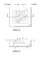
- FIG. 1shows a sensor 10, in accordance with the present invention.
- Sensor 10includes a sensor substrate 12, sensing elements 14, 16, 18, and 20, and electronic switching circuit 22.
- the sensing elements 14-20are preferably formed by implantation, diffusion, thin-film deposition, or other well known techniques.
- Switching circuit 22is electrically connected to each of the sensing elements 14-20 via lines 28, 30, 32, 34, 36, 38, 40, and 42 for electrically selecting at least one of the sensing elements 14-20.
- Lines 28, 32, 36, and 42preferably carry a S + (positive sensor output) signal and lines 30, 34, 38, and 40 preferably carry a S - (negative sensor output) signal.
- Switching circuit 22is preferably formed on substrate 12 by a standard semiconductor fabrication process or other well known techniques.
- switching circuit 22selects the desired sensor element for measurement by electrically (digitally) connecting the S + and S - terminals of the sensor to a signal conditioning circuit which measures the differential output voltage of each defined sensing element 14-20 and amplifies and compensates the desired sensing element output signals for use by an external system.
- powerV + and V -
- sensing elements 14-20are selected by connecting the desired output signal terminals S + and S - .
- Other switching configurationscan also be used. For example, all S + , S - , and V + leads could be connected to circuit 22 and then switching in the appropriate V - connection for the desired element (see FIG. 8 below). Other alternative embodiments are described in detail below.
- Sensing elements 14-20are preferably deposed at varying distances from an outer edge 44 of a cavity 51. It is well known that sensors provide the best performance when the sensing elements are placed adjacent an edge of the diaphragm 46. Also, a sensor's sensitivity is a function of diaphragm thickness and size. By placing the elements 14-20 at varying distances from the edge 44 of the cavity opening an inexpensive timed etch method can be used. In this way, the edge of the diaphragm 46 can be formed essentially at one of the edges 43, 45, 47, and 49 as indicated in FIGS. 2 and 3.
- a repeated etch and measurement cycle to measure diaphragm thickness and stop etching at a precise nominal diaphragm thicknesscan be minimized. This is because of the ability of the sensor 10 to operate nominally across a range of four diaphragm 46 thicknesses each corresponding to a different diaphragm edge 43, 45, 47, 49 located relative to one of the corresponding elements 14, 16, 18, 20.
- the etching process timing windowis widened by virtue of a wider range of diaphragm thicknesses that still produce usable sensors 10. The possibility of over-etch or under-etch is reduced because of an increase in the target diaphragm thickness window.
- FIGS. 2 and 3show four possible diaphragm 46 thicknesses with corresponding diaphragm edges 43, 45, 47, and 49 defining the optimal edges of diaphragm 46 for each of the sensing elements 14-20. It is noted that each of the sensing elements 14-20 are preferably positioned on substrate 12 directly above one of the edges 43-49 for optimum performance.
- the on-chip switching circuit 22is needed to select the element 14-20 that provides performance closest to the nominal target.
- FIGS. 4, 5, and 6are cross-sectional views of various stages of a preferred method of manufacture of the sensor 10.
- FIG. 4shows the first step of the method where a sensing substrate 12 is provided and preferably made of silicon or other suitable material.
- Substrate 12has a top surface 50 opposed to a bottom surface 52.
- FIG. 5shows the next step of deposing sensing elements 14-20 and electronic switching circuit 22 on the top surface 50. It is noted that electrical interconnect lines 28-42 are also formed at this time but are not shown.
- FIG. 6shows the final step of removing a portion of substrate 12 from the bottom surface 52 through an etching process to form a cavity 51 to form a diaphragm 46. It is noted that a timed-etch process is preferred but any etching process could be employed depending on the precision required in the placement of the elements 14-20 and the thickness of the diaphragm 46.
- FIG. 7discloses an alternate embodiment in accordance with the present invention.
- Electronic switching circuit 24selects the desired sensing elements 114-120.
- the circuit 24is preferably on-chip (monolithic), but may be off-chip as well.
- Sensor 55is similar to sensor 10 described above except that sensor 55 has electronic switching circuit 24 instead of circuit 22.
- Circuit 24 deposed on substrate 57has a switched electrical connection with the sensing elements via lines 54, 56, 58, and 60 as shown for electronically powering at least one of the sensing elements.
- one of lines 54, 56, 58, and 60connects the sensor V - terminal (ground terminal) to the power supply by selecting an appropriate digital code that is implemented by the switching circuit 24.
- FIG. 8discloses yet another preferred embodiment in accordance with the present invention.
- the sensor 66includes a substrate 68, having a diaphragm 70 defined by edge 72, sensing elements 74, 76, 78 and 80, and a switching circuit defined by box 82.
- Switching circuit 82includes 12 switches 84, which are preferably FETS as shown. The switches 84 are connected to one of the four input terminals 86, 88, 90, and 92.
- input terminals 86-92are connected to a microprocessor (not shown) or other logic circuitry and select the sensing element to be used. For example, if sensing element 74 is to be used, a signal would be sent through terminal 86 causing the three transistors 84 associated with the element 74 to turn on causing a signal to be outputted to terminals 94 and 96 from element 74. As can be seen, each of the elements 74-80 is always connected to the high-side voltage terminal 98. Switching the low-side power supply voltage terminal and the two output signal terminals of each element 74-80 ensures a clean signal is supplied to terminals 94 and 96. As disclosed above, the sensor can select an element by switching only the power or switching the output terminals. However, by switching both a power terminal and the output terminals, a cleaner signal at terminals 94 & 96 is caused.
- the technique described aboveselects elements to accommodate process variations in cavity etch and diaphragm edge location.
- the sensorscan also be used to make multiple pressure sensor range die. Instead of placing sensing elements on a substrate to cover a wider range of etch conditions for a single targeted pressure range, sensing elements can be placed so that they are optimized for different pressure ranges. Each sensing element has its own target diaphragm size (cavity edge) and thickness. This may be done in conjunction with the same or different size cavity. Generally, the thicker the diaphragm 46 the higher the pressure range that will be sensed by sensor 10.
- a sensor 10 having a diaphragm edge corresponding with line 43 and having a thicker diaphragmwill be used for a higher pressure range than a sensor 10 having a diaphragm edge corresponding to any of lines 45-49 and having a thinner diaphragm.
- An advantage of this inventionis that only one integrated sensor design, mask set, and fabrication process is needed for the top side of the substrate. The top side of the substrate is where the complicated and costly signal conditioning and wafer processing is done. By only modifying the etch time and/or the backside cavity opening (this is only one low cost mask), four different pressure range sensors can be manufactured from the same integrated circuit wafers.
Landscapes
- Physics & Mathematics (AREA)
- General Physics & Mathematics (AREA)
- Measuring Fluid Pressure (AREA)
- Pressure Sensors (AREA)
- Semiconductor Integrated Circuits (AREA)
Abstract
Description
Claims (11)
Priority Applications (6)
| Application Number | Priority Date | Filing Date | Title |
|---|---|---|---|
| US09/137,765US6142021A (en) | 1998-08-21 | 1998-08-21 | Selectable pressure sensor |
| EP99946594AEP1110067B1 (en) | 1998-08-21 | 1999-08-12 | Sensor with diaphragm and a plurality of switchable transducers to hit the edge |
| JP2000566649AJP2002523736A (en) | 1998-08-21 | 1999-08-12 | Pressure sensor and method of forming the same |
| ES99946594TES2217809T3 (en) | 1998-08-21 | 1999-08-12 | SENSOR WITH DIAPHRAGM AND A PLURALITY OF SWITCHING TRANSDUCERS TO FIND THE EDGE. |
| DE69915651TDE69915651T2 (en) | 1998-08-21 | 1999-08-12 | Sensor with membrane and a variety of switchable transducers to hit the edge |
| PCT/US1999/018474WO2000011441A2 (en) | 1998-08-21 | 1999-08-12 | Pressure sensor and method of forming the same |
Applications Claiming Priority (1)
| Application Number | Priority Date | Filing Date | Title |
|---|---|---|---|
| US09/137,765US6142021A (en) | 1998-08-21 | 1998-08-21 | Selectable pressure sensor |
Publications (1)
| Publication Number | Publication Date |
|---|---|
| US6142021Atrue US6142021A (en) | 2000-11-07 |
Family
ID=22478952
Family Applications (1)
| Application Number | Title | Priority Date | Filing Date |
|---|---|---|---|
| US09/137,765Expired - LifetimeUS6142021A (en) | 1998-08-21 | 1998-08-21 | Selectable pressure sensor |
Country Status (6)
| Country | Link |
|---|---|
| US (1) | US6142021A (en) |
| EP (1) | EP1110067B1 (en) |
| JP (1) | JP2002523736A (en) |
| DE (1) | DE69915651T2 (en) |
| ES (1) | ES2217809T3 (en) |
| WO (1) | WO2000011441A2 (en) |
Cited By (3)
| Publication number | Priority date | Publication date | Assignee | Title |
|---|---|---|---|---|
| US20090189629A1 (en)* | 2007-12-27 | 2009-07-30 | Ross Holger | Semiconductor wafer having a multitude of sensor elements and method for measuring sensor elements on a semiconductor wafer |
| US20100180687A1 (en)* | 2009-01-16 | 2010-07-22 | Infineon Technologies Ag | Pressure sensor including switchable sensor elements |
| US9395259B2 (en) | 2012-11-21 | 2016-07-19 | Continental Automotive Systems, Inc. | Piezoresistive transducer with low thermal noise |
Families Citing this family (1)
| Publication number | Priority date | Publication date | Assignee | Title |
|---|---|---|---|---|
| US6790699B2 (en) | 2002-07-10 | 2004-09-14 | Robert Bosch Gmbh | Method for manufacturing a semiconductor device |
Citations (7)
| Publication number | Priority date | Publication date | Assignee | Title |
|---|---|---|---|---|
| US4322980A (en)* | 1979-11-08 | 1982-04-06 | Hitachi, Ltd. | Semiconductor pressure sensor having plural pressure sensitive diaphragms and method |
| US4539554A (en)* | 1982-10-18 | 1985-09-03 | At&T Bell Laboratories | Analog integrated circuit pressure sensor |
| US4885621A (en)* | 1988-05-02 | 1989-12-05 | Delco Electronics Corporation | Monolithic pressure sensitive integrated circuit |
| US4996082A (en)* | 1985-04-26 | 1991-02-26 | Wisconsin Alumni Research Foundation | Sealed cavity semiconductor pressure transducers and method of producing the same |
| US5220838A (en)* | 1991-03-28 | 1993-06-22 | The Foxboro Company | Overpressure-protected, differential pressure sensor and method of making the same |
| US5264075A (en)* | 1992-11-06 | 1993-11-23 | Ford Motor Company | Fabrication methods for silicon/glass capacitive absolute pressure sensors |
| US5531121A (en)* | 1993-05-10 | 1996-07-02 | Delco Electronics Corporation | Micromachined integrated pressure sensor with oxide polysilicon cavity sealing |
Family Cites Families (9)
| Publication number | Priority date | Publication date | Assignee | Title |
|---|---|---|---|---|
| US3456226A (en)* | 1967-10-27 | 1969-07-15 | Conrac Corp | Strain gage configuration |
| JPS5217780A (en)* | 1975-07-04 | 1977-02-09 | Hitachi Ltd | Pressure convertor with semi-conductor elements |
| US4400681A (en)* | 1981-02-23 | 1983-08-23 | General Motors Corporation | Semiconductor pressure sensor with slanted resistors |
| CA1186163A (en)* | 1982-01-04 | 1985-04-30 | James B. Starr | Semiconductor pressure transducer |
| JPS6077470A (en)* | 1983-10-04 | 1985-05-02 | Nec Corp | Diaphragm type semiconductor pressure sensor |
| US5058435A (en)* | 1989-06-22 | 1991-10-22 | Ic Sensors, Inc. | Single diaphragm transducer with multiple sensing elements |
| WO1995002164A1 (en)* | 1993-07-07 | 1995-01-19 | Ic Sensors, Inc. | Pulsed thermal flow sensor system |
| DE19527687A1 (en)* | 1995-07-28 | 1997-01-30 | Bosch Gmbh Robert | sensor |
| US5672808A (en)* | 1996-06-11 | 1997-09-30 | Moore Products Co. | Transducer having redundant pressure sensors |
- 1998
- 1998-08-21USUS09/137,765patent/US6142021A/ennot_activeExpired - Lifetime
- 1999
- 1999-08-12WOPCT/US1999/018474patent/WO2000011441A2/enactiveIP Right Grant
- 1999-08-12ESES99946594Tpatent/ES2217809T3/ennot_activeExpired - Lifetime
- 1999-08-12DEDE69915651Tpatent/DE69915651T2/ennot_activeExpired - Lifetime
- 1999-08-12JPJP2000566649Apatent/JP2002523736A/enactivePending
- 1999-08-12EPEP99946594Apatent/EP1110067B1/ennot_activeExpired - Lifetime
Patent Citations (7)
| Publication number | Priority date | Publication date | Assignee | Title |
|---|---|---|---|---|
| US4322980A (en)* | 1979-11-08 | 1982-04-06 | Hitachi, Ltd. | Semiconductor pressure sensor having plural pressure sensitive diaphragms and method |
| US4539554A (en)* | 1982-10-18 | 1985-09-03 | At&T Bell Laboratories | Analog integrated circuit pressure sensor |
| US4996082A (en)* | 1985-04-26 | 1991-02-26 | Wisconsin Alumni Research Foundation | Sealed cavity semiconductor pressure transducers and method of producing the same |
| US4885621A (en)* | 1988-05-02 | 1989-12-05 | Delco Electronics Corporation | Monolithic pressure sensitive integrated circuit |
| US5220838A (en)* | 1991-03-28 | 1993-06-22 | The Foxboro Company | Overpressure-protected, differential pressure sensor and method of making the same |
| US5264075A (en)* | 1992-11-06 | 1993-11-23 | Ford Motor Company | Fabrication methods for silicon/glass capacitive absolute pressure sensors |
| US5531121A (en)* | 1993-05-10 | 1996-07-02 | Delco Electronics Corporation | Micromachined integrated pressure sensor with oxide polysilicon cavity sealing |
Cited By (7)
| Publication number | Priority date | Publication date | Assignee | Title |
|---|---|---|---|---|
| US20090189629A1 (en)* | 2007-12-27 | 2009-07-30 | Ross Holger | Semiconductor wafer having a multitude of sensor elements and method for measuring sensor elements on a semiconductor wafer |
| US7872487B2 (en)* | 2007-12-27 | 2011-01-18 | Robert Bosch Gmbh | Semiconductor wafer having a multitude of sensor elements and method for measuring sensor elements on a semiconductor wafer |
| US20100180687A1 (en)* | 2009-01-16 | 2010-07-22 | Infineon Technologies Ag | Pressure sensor including switchable sensor elements |
| US7926353B2 (en)* | 2009-01-16 | 2011-04-19 | Infineon Technologies Ag | Pressure sensor including switchable sensor elements |
| US20110146410A1 (en)* | 2009-01-16 | 2011-06-23 | Infineon Technologies Ag | Pressure sensor including switchable sensor elements |
| US8127619B2 (en) | 2009-01-16 | 2012-03-06 | Infineon Technologies Ag | Pressure sensor including switchable sensor elements |
| US9395259B2 (en) | 2012-11-21 | 2016-07-19 | Continental Automotive Systems, Inc. | Piezoresistive transducer with low thermal noise |
Also Published As
| Publication number | Publication date |
|---|---|
| WO2000011441A3 (en) | 2000-06-02 |
| WO2000011441A2 (en) | 2000-03-02 |
| EP1110067A4 (en) | 2001-10-24 |
| JP2002523736A (en) | 2002-07-30 |
| DE69915651D1 (en) | 2004-04-22 |
| EP1110067A2 (en) | 2001-06-27 |
| DE69915651T2 (en) | 2004-08-19 |
| ES2217809T3 (en) | 2004-11-01 |
| EP1110067B1 (en) | 2004-03-17 |
Similar Documents
| Publication | Publication Date | Title |
|---|---|---|
| US6167761B1 (en) | Capacitance type pressure sensor with capacitive elements actuated by a diaphragm | |
| US7493822B2 (en) | Small gauge pressure sensor using wafer bonding and electrochemical etch stopping | |
| US5155061A (en) | Method for fabricating a silicon pressure sensor incorporating silicon-on-insulator structures | |
| US4766666A (en) | Semiconductor pressure sensor and method of manufacturing the same | |
| US6912759B2 (en) | Method of manufacturing a thin piezo resistive pressure sensor | |
| US7000298B2 (en) | Method a quartz sensor | |
| US6861276B2 (en) | Method for fabricating a single chip multiple range pressure transducer device | |
| US7997142B2 (en) | Low pressure sensor device with high accuracy and high sensitivity | |
| US6122975A (en) | CMOS compatible integrated pressure sensor | |
| US8381596B2 (en) | CMOS compatible pressure sensor for low pressures | |
| US6725725B1 (en) | Micromechanical differential pressure sensor device | |
| JPH06307960A (en) | Pressure sensor | |
| US20050132813A1 (en) | Sealed diaphragm pressure sensor | |
| US5095349A (en) | Semiconductor pressure sensor and method of manufacturing same | |
| USRE34893E (en) | Semiconductor pressure sensor and method of manufacturing same | |
| US8647908B2 (en) | Semiconductor pressure sensor and method of manufacturing semiconductor pressure sensor | |
| US6142021A (en) | Selectable pressure sensor | |
| US6933582B2 (en) | Semiconductor sensor having a diffused resistor | |
| US4881056A (en) | Facedown-type semiconductor pressure sensor with spacer | |
| JP2789291B2 (en) | Pressure sensor | |
| JPH04299871A (en) | Semiconductor pressure sensor and its manufacture | |
| US7179668B2 (en) | Technique for manufacturing silicon structures | |
| EP3299787B1 (en) | Cmos and pressure sensor integrated on a chip and fabrication method | |
| JP2000124466A (en) | Semiconductor pressure sensor and its manufacture | |
| JP2519393B2 (en) | Method for manufacturing semiconductor dynamic quantity sensor |
Legal Events
| Date | Code | Title | Description |
|---|---|---|---|
| AS | Assignment | Owner name:MOTOROLA, INC., ILLINOIS Free format text:ASSIGNMENT OF ASSIGNORS INTEREST;ASSIGNORS:ROSS, CARL;CZARNOCKI, WALTER;SCHUSTER, JOHN;AND OTHERS;REEL/FRAME:009401/0189 Effective date:19980820 | |
| STCF | Information on status: patent grant | Free format text:PATENTED CASE | |
| FPAY | Fee payment | Year of fee payment:4 | |
| AS | Assignment | Owner name:TEMIC AUTOMOTIVE OF NORTH AMERICA, INC., ILLINOIS Free format text:ASSIGNMENT OF ASSIGNORS INTEREST;ASSIGNOR:MOTOROLA, INC.;REEL/FRAME:018471/0188 Effective date:20061016 | |
| FPAY | Fee payment | Year of fee payment:8 | |
| FEPP | Fee payment procedure | Free format text:PAYOR NUMBER ASSIGNED (ORIGINAL EVENT CODE: ASPN); ENTITY STATUS OF PATENT OWNER: LARGE ENTITY | |
| FPAY | Fee payment | Year of fee payment:12 | |
| AS | Assignment | Owner name:CONTINENTAL AUTOMOTIVE SYSTEMS, INC., MICHIGAN Free format text:MERGER;ASSIGNORS:CONTINENTAL TEVES, INC.;TEMIC AUTOMOTIVE OF NORTH AMERICA, INC,;REEL/FRAME:033135/0185 Effective date:20091210 |