US6141248A - DRAM and SRAM memory cells with repressed memory - Google Patents
DRAM and SRAM memory cells with repressed memoryDownload PDFInfo
- Publication number
- US6141248A US6141248AUS09/362,909US36290999AUS6141248AUS 6141248 AUS6141248 AUS 6141248AUS 36290999 AUS36290999 AUS 36290999AUS 6141248 AUS6141248 AUS 6141248A
- Authority
- US
- United States
- Prior art keywords
- gate
- transistor
- source
- information
- mode
- Prior art date
- Legal status (The legal status is an assumption and is not a legal conclusion. Google has not performed a legal analysis and makes no representation as to the accuracy of the status listed.)
- Expired - Lifetime
Links
- 230000015654memoryEffects0.000titleclaimsabstractdescription157
- 239000003990capacitorSubstances0.000claimsabstractdescription37
- 238000007667floatingMethods0.000claimsdescription87
- 230000005641tunnelingEffects0.000claimsdescription21
- 238000000034methodMethods0.000claimsdescription18
- 229910021420polycrystalline siliconInorganic materials0.000claimsdescription12
- 229920005591polysiliconPolymers0.000claimsdescription12
- 230000004044responseEffects0.000claimsdescription11
- XUIMIQQOPSSXEZ-UHFFFAOYSA-NSiliconChemical compound[Si]XUIMIQQOPSSXEZ-UHFFFAOYSA-N0.000claimsdescription6
- 229910052710siliconInorganic materials0.000claimsdescription6
- 239000010703siliconSubstances0.000claimsdescription6
- 230000003068static effectEffects0.000claimsdescription6
- 229910052814silicon oxideInorganic materials0.000claimsdescription5
- -1silicon oxide nitrideChemical class0.000claimsdescription5
- 230000003213activating effectEffects0.000claimsdescription4
- 230000008878couplingEffects0.000claims3
- 238000010168coupling processMethods0.000claims3
- 238000005859coupling reactionMethods0.000claims3
- 238000013500data storageMethods0.000claims3
- 238000010586diagramMethods0.000description10
- VYPSYNLAJGMNEJ-UHFFFAOYSA-NSilicium dioxideChemical compoundO=[Si]=OVYPSYNLAJGMNEJ-UHFFFAOYSA-N0.000description6
- 230000000694effectsEffects0.000description6
- 239000012535impuritySubstances0.000description6
- 239000000758substrateSubstances0.000description6
- 239000004065semiconductorSubstances0.000description4
- 229910052681coesiteInorganic materials0.000description3
- 229910052906cristobaliteInorganic materials0.000description3
- 238000009792diffusion processMethods0.000description3
- 239000000377silicon dioxideSubstances0.000description3
- 229910052682stishoviteInorganic materials0.000description3
- 229910052905tridymiteInorganic materials0.000description3
- 229910007277Si3 N4Inorganic materials0.000description2
- 230000002411adverseEffects0.000description2
- 230000002708enhancing effectEffects0.000description2
- 239000012212insulatorSubstances0.000description2
- 239000000463materialSubstances0.000description2
- 150000004767nitridesChemical class0.000description2
- 230000008569processEffects0.000description2
- 102100037807GATOR complex protein MIOSHuman genes0.000description1
- 101000950705Homo sapiens GATOR complex protein MIOSProteins0.000description1
- 230000004075alterationEffects0.000description1
- 230000009286beneficial effectEffects0.000description1
- 230000015572biosynthetic processEffects0.000description1
- 239000002131composite materialSubstances0.000description1
- 238000004883computer applicationMethods0.000description1
- 238000010276constructionMethods0.000description1
- 230000007547defectEffects0.000description1
- 238000001514detection methodMethods0.000description1
- 239000003989dielectric materialSubstances0.000description1
- 238000005516engineering processMethods0.000description1
- 230000005669field effectEffects0.000description1
- 230000006870functionEffects0.000description1
- 238000012417linear regressionMethods0.000description1
- 239000011159matrix materialSubstances0.000description1
- 229910021421monocrystalline siliconInorganic materials0.000description1
- 239000002159nanocrystalSubstances0.000description1
- 230000002093peripheral effectEffects0.000description1
- 238000004886process controlMethods0.000description1
- 230000000717retained effectEffects0.000description1
- 125000006850spacer groupChemical group0.000description1
- 238000006467substitution reactionMethods0.000description1
Images


Classifications
- G—PHYSICS
- G11—INFORMATION STORAGE
- G11C—STATIC STORES
- G11C14/00—Digital stores characterised by arrangements of cells having volatile and non-volatile storage properties for back-up when the power is down
Definitions
- the present inventionrelates to the field of semiconductor memory devices and, more particularly to a dynamic random access memory (DRAM) cell with a non-volatile memory component and a static random access memory (SRAM) cell with a non-volatile memory component.
- DRAMdynamic random access memory
- SRAMstatic random access memory
- An essential semiconductor deviceis semiconductor memory, such as a random access memory (RAM) device.
- RAMrandom access memory
- a RAM deviceallows the user to execute both read and write operations on its memory cells.
- Typical examples of RAM devicesinclude dynamic random access memory (DRAM) and static random access memory (SRAM).
- DRAMis a specific category of RAM containing an array of individual memory cells, where each cell includes a capacitor for holding a charge and a transistor for accessing the charge held in the capacitor.
- the transistoris often referred to as the access transistor or the transfer device of the DRAM cell.
- FIG. 1illustrates a portion of a DRAM memory circuit containing two neighboring DRAM cells 10.
- Each cell 10contains a storage capacitor 14 and an access field effect transistor or transfer device 12.
- a reference voltageillustrated as a ground potential for convenience purposes.
- the other side of the storage capacitor 14is connected to the drain of the transfer device 12.
- the gate of the transfer device 12is connected to a signal known in the art as a word line 18.
- the source of the transfer device 12is connected to a signal known in the art as a bit line 16 (also known in the art as a digit line).
- each cell 10contains one bit of data (i.e., a logic "0” or logic "1").
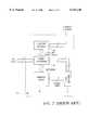
- the DRAM 40contains a memory array 42, row and column decoders 44, 48 and a sense amplifier circuit 46.
- the memory array 42consists of a plurality of memory cells (constructed as illustrated in FIG. 1) whose word lines and bit lines are commonly arranged into rows and columns, respectively.
- the bit lines of the memory array 42are connected to the sense amplifier circuit 46, while its word lines are connected to the row decoder 44.
- Address and control signalsare input into the DRAM 40 and connected to the column decoder 48, sense amplifier circuit 46 and row decoder 44 and are used to gain read and write access, among other things, to the memory array 42.
- the column decoder 48is connected to the sense amplifier circuit 46 via control and column select signals.
- the sense amplifier circuit 46receives input data destined for the memory array 42 and outputs data read from the memory array 42 over input/output (I/O) data lines. Data is read from the cells of the memory array 42 by activating a word line (via the row decoder 44), which couples all of the memory cells corresponding to that word line to respective bit lines, which define the columns of the array. One or more bit lines are also activated.
- the sense amplifier circuit 46 connected to a bit line columndetects and amplifies the data bit transferred from the storage capacitor of the memory cell to its bit line by measuring the potential difference between the activated bit line and a reference line which may be an inactive bit line.
- a reference linewhich may be an inactive bit line.
- DRAM devicesare the most cost effective high speed memory used with computers and computer systems. They last (nearly) indefinitely and are available in very high density. They are, however, limited in the longevity of their memory. DRAM devices require constant refreshing and lose all knowledge of their state (i.e., contents) once power to the device is removed. It is desirable to have a memory device, such as a DRAM memory device, with all of the positive features of DRAM devices, e.g., cost, size, speed, availability, etc., that retains its memory state when power is removed from the device. That is, it is desirable to have DRAM cells with a nonvolatile memory component built within the cell.
- a DRAM cell with a nonvolatile componentwould be very beneficial in numerous computer systems and computer applications.
- One applicationwould be the saving and/or restoring of the state of a central processing unit (CPU) that is executing software instructions in a protected mode of operation, an example of which is disclosed in U.S. Pat. No. 5,497,494 to Combs et al., which is hereby incorporated by reference in its entirety.
- This applicationtypically involves the use of memory separate from the main memory of the computer, typically referred to as shadow RAM, from which a BIOS program is executed and the CPU state is to be stored to and retrieved from.
- Having a DRAM device constructed with DRAM cells having a nonvolatile componentwould eliminate the need to have the separate shadow RAM.
- a main memorycontains data and error detection codes associated with each piece of data.
- a separate shadow memoryis used to store data corresponding to the data stored in the main memory. If the system determines that accessed data from the main memory is erroneous, the corresponding data from the shadow memory is used and thus, faults in the main memory do not adversely effect the system (i.e., the system is fault tolerant). Again, memory separate from the main memory is required, which adds cost and adds to the size and complexity of the system. Having a DRAM device constructed with DRAM cells having a nonvolatile component would eliminate the need to have the separate shadow memory.
- SRAM devicesare another form of RAM device. SRAM devices differ from DRAM devices in that they do not require constant refreshing.
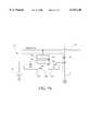
- a standard SRAM cell 200is shown in FIG. 3a. Cell 200 consists of four transistors 206, 208, 210, 212, and two control transistors 202 and 204. Data is stored with either a high potential at node A and a low potential at node B, or a low potential at node A and a high potential at node B. This means that two stable states are available which are defined as a logic "1" or a logic "0".
- a typical SRAMconsists of a matrix of storage bits with bit capacity 2 N ⁇ 2 M bits arranged in an array 275 with 2 M columns (bit lines) and 2 N rows (word lines).
- a row addressis input and decoded by row decoder 280 to select one of the rows or word lines. All of the cells along this word line are activated.
- Column decoder 282then addresses one bit out of the 2 M bits that have been activated and routes the data that is stored in that bit to a sense amplifier (not shown) and then out of the array 275. Data in and Data out are controlled by the Read/Write Control circuit 284.
- the logic state of SRAM cell 200i.e., either a "1” or "0" is read by sensing the cell current on bit line pair comprised of bit lines 216 and 217 and/or the differential voltage developed thereon.
- word line 218When word line 218 is selected, cell 200 is activated by turning on control transistors 202 and 204. If the activated SRAM cell 200 is in logic state "1" node A is high and node B is low. Transistor 208 will be off, transistor 212 will be on, transistor 206 will be on, and transistor 210 will be off. Since transistors 212 and 204 are on, bit line 217 will carry cell current, while bit line 216 will not carry any cell current since transistor 208 is off.
- FIG. 3billustrates an alternative SRAM cell 250.
- transistors 206 and 210are replaced by two resistors 252, 254.
- the operation of the cell 250is essentially the same as the operation of the cell 200 (FIG. 3a).
- the SRAM cell 250can also be used in and accessed from the SRAM device illustrated in FIG. 4.
- SRAM deviceshave their advantages, e.g., they do not require constant refreshing, they are not without their shortcomings. For example, similar to DRAM devices, SRAM devices also lose all knowledge of their state once power to the device is removed. A SRAM utilizing SRAM cells having a nonvolatile component would also be suitable for use in a computer system for startup/restart from protected mode and other shadow memory applications. Accordingly, there is a desire and need for a SRAM memory device that retains its memory state when power is removed from the device. That is, it is desirable to have SRAM cells with a nonvolatile memory component built within the cell.
- the present inventionprovides a DRAM cell with a nonvolatile memory component built within the cell.
- the present inventionalso provides a SRAM cell with a nonvolatile memory component built within the cell.
- the above and other features and advantages of the inventionare achieved by replacing the transfer device of a typical DRAM cell with a transistor having an additional gate.
- the unique cellcan be accessed as a typical DRAM cell by reading from or writing to a storage capacitor.
- the cellcan be accessed as a nonvolatile cell by storing a charge onto the additional gate (representative of one logic value) or erasing the charge from the additional gate (representative of another logic value) using a tunneling technique. Contents of the additional gate are retained even if power is removed from the cell.
- the DRAM cellhas a nonvolatile component built into its cell. Whether a charge is stored on the additional gate is determined by a unique data sensing method.
- the methodutilizes a response time of the cell to determine whether or not the additional gate contains a charge and thus, determines the logic value of the data within the cell.
- a DRAM cell having a nonvolatile memory component within its cellis formed in a simple and cost effective manner.
- Transistors in a typical SRAM cellare also replaced by the transistors with the additional gate to form a SRAM cell having a nonvolatile component built within its cell.
- FIG. 1is a circuit diagram illustrating conventional dynamic random access memory (DRAM) cells
- FIG. 2is a block diagram illustrating a DRAM device
- FIGS. 3a and 3bare circuit diagrams illustrating conventional static random access memory (SRAM) cells
- FIG. 4is a block diagram illustrating a SRAM device
- FIGS. 5a and 5bare circuit diagrams illustrating DRAM cells constructed in accordance with an embodiment of the present invention.
- FIG. 6illustrates an exemplary process for sensing the state of the nonvolatile memory component of the DRAM cells illustrated in FIGS. 5a and 5b;
- FIGS. 7a and 7billustrate a sense amplifier voltage response over time associated with the sensing of the contents of the DRAM cells illustrated in FIGS. 5a and 5b;
- FIGS. 8a and 8bare circuit diagrams illustrating SRAM cells constructed in accordance with an embodiment of the present invention.
- FIG. 9illustrates a block diagram of a computer system utilizing either the DRAM cells illustrated in FIGS. 5a and 5b or the SRAM cells illustrated in FIGS. 8a and 8b;
- FIG. 10illustrates a silicon oxide nitride oxide silicon (SONOS) memory device constructed in accordance with the present invention.
- SONOSsilicon oxide nitride oxide silicon
- FIGS. 5a and 5bare circuit diagrams illustrating DRAM cells 100 constructed in accordance with an embodiment of the present invention.
- the cells 100are similar to the cells 10 illustrated in FIG. 1 with the exception that a different transfer device 112 replaces the transfer device 12 (FIG. 1).
- the transfer device 112is a transistor having a control gate 114 and an additional gate 116, often referred to as a floating gate, and is of the kind often used in flash memory devices.
- the transfer device 112has a drain 118 connected to one end of the storage capacitor 14 and a source 122 connected to the bit line 16 (as in the conventional DRAM cell 10 illustrated in FIG. 1).
- the source 122 and drain 118are constructed from a N+ type region of high impurity concentration formed on a P-type semiconductor substrate 120 and are separated by a channel region 120a. It is desirable that the floating gate 116 be constructed from polysilicon. It is also desirable that the floating gate 116 be is isolated from the control gate 114 by a dielectric material 124 and from the source 122, drain 118 and channel 120a by a thin layer of oxide 126. As will be described below, the use of the transfer device 112 allows the cell 100 of the present invention to be operated as either a conventional DRAM cell or as a nonvolatile memory cell (herein referred to as a DRAM with "repressed memory").
- the floating gate 116may contain a charge on it. This charge may slightly alter the characteristics (e.g., resistance) of the transfer device 112. For example, the transfer of information to/from the bit line 16 may be slower in the cell 100 of the present invention when compared to a similar transfer in the conventional DRAM cell 10 illustrated in FIG. 1.
- a tunnel-tunnel mode of operationwill be used to program one of two different charge states onto the floating gate 116 (and thus, program the transfer device 112 into one of two states). That is, a tunnel mode is used to transfer electrons from the source 122 to the floating gate 116 to program the transfer device 112, its gate 116 and thus, the nonvolatile portion of the cell 100, to a first charge state (i.e., tunnel write operation). This is accomplished by driving the floating gate 116 (through the control gate 114 and word line 18) with a large positive voltage, such as, for example, twelve or fifteen volts, while grounding the source 122 (via the bit line 16).
- a large positive voltagesuch as, for example, twelve or fifteen volts
- this negative chargecan be associated with either a logic “0" or "1” and that the invention is not limited to any particular association between the first charge state and a particular logic value.
- the one requirementis that the program, erase and sensing circuitry used to access the nonvolatile portion of the cell 100 associate the first charge state to the same logic value.
- a tunnel modeis used to transfer the electrons from the floating gate 116 to the source 122 to program the transfer device 112, its gate 116 and thus, the nonvolatile portion of the cell 100, to a second charge state (i.e., tunnel erase operation).
- Thisis accomplished by driving the floating gate 116 (through the control gate 114 and word line 18) with a large negative voltage, such as, for example, negative seven or ten volts, while driving the source 122 (via the bit line 16) with a positive voltage, such as, for example, five volts.
- a large negative voltagesuch as, for example, negative seven or ten volts
- the source 122via the bit line 16
- a positive voltagesuch as, for example, five volts.
- the lack of a negative charge on the floating gate 116can be associated with either a logic “0" or "1” and that the invention is not limited to any particular association between the second charge state and a particular logic value.
- the one requirementis that the program, erase and sensing circuitry used to access the nonvolatile portion of the cell 100 associate the second charge state to the same logic value and that the logic value be different than the value chosen for the first charge state.
- step 502it must be determined whether the cell is being accessed as a DRAM or as a nonvolatile memory (step 502). If the cell is to be operated as a DRAM, a voltage in excess of the normal threshold voltage of the cell's transfer device is applied to the control gate of the cell (step 510). A charge on the floating gate may effect the characteristics (e.g., resistance) of the transfer device and its threshold voltage. A difference in threshold voltage of the transfer device will have no effect on the potential transferred to the bit line, but it will effect the rate at which it is transferred. The difference in threshold voltage and resistance of the transfer device determines only the current, but the DRAM sense amplifiers respond only to potential differences.
- a voltage in excess of the normal threshold voltage of the cell's transfer deviceis applied to the control gate of the cell (step 510).
- a charge on the floating gatemay effect the characteristics (e.g., resistance) of the transfer device and its threshold voltage.
- a difference in threshold voltage of the transfer devicewill have no effect on the potential transferred to the bit line, but
- the word lineis driven to a voltage as far as possible in excess of the threshold voltage of the transfer device to minimize the resistance of the transfer device (typically a few thousand ohms). This results in the charge stored in the capacitor being transferred to the bit line in a sub-nanosecond time period.
- the sense amplifiersubsequently responds with either a sensed Vout + or a Vout - (depending upon the charge stored in the capacitor) after time t S whether or not the floating gate is in the first charge state (step 512). Once the sense amplifier has sensed the potential on the bit line, the appropriate data value may be output (step 508).
- a voltage that is approximately equal to the typical threshold voltage of the cell transfer deviceis applied to the control gate of the cell (step 504). This will cause the charge stored on the capacitor to be transferred to the bit line. This charge is not being used for its data value since it represents the stored DRAM value. Instead, as will be described below, the charge is being used to determine the response time of the sense amplifier, since the response time is indicative of whether the transfer device is programmed to the first or second charge state (step 506).
- a charge on the floating gatemay effect the characteristics (e.g., resistance) of the transfer device and its threshold voltage.
- the characteristicswill vary depending upon the threshold voltage. For example, if the threshold voltage is high, e.g., 0.6 volts, the transfer device has a higher resistance and it will not conduct well. This would represent the case when electrons are stored on the floating gate. That is, the floating gate is programmed to the first charge state. Likewise, if the threshold voltage is low, e.g., 0.0 volts, the transfer device has a low resistance and it will conduct much better. This would represent the case when electrons are not stored on the floating gate. That is, the floating gate is programmed to the second charge state.
- the resistance of the transfer devicecan be sensed.
- the resistancewill determine the response time of the sense amplifier. If the transfer device has a high resistance because it has been programmed to the first charge state, the stored charge from the storage capacitor (whose value is not important) is transferred to the bit line much slower in comparison to the transfer of the charge described in steps 510 and 512 (i.e., DRAM operation).
- the sense amplifiersubsequently responds with, for example, a sensed Vout + after time t S + ⁇ t (see FIG. 7b). It should be appreciated that the first charge state can be associated with a sensed Vout - instead of the Vout + .
- the transfer devicehas a low resistance because it has been programmed with the second charge state, the stored charge from the storage capacitor (whose value is not important) is transferred to the bit line at approximately the same speed as the transfer of the charge described in steps 510 and 512 (i.e., DRAM operation).
- the sense amplifiersubsequently responds with, for example, a sensed Vout - after time t S (see FIG. 7b).
- the second charge statecan be associated with a sensed Vout + instead of the Vout - .
- the cell 100can be operated as a DRAM and a nonvolatile memory and is suitable for use in many applications and systems that require both DRAM and nonvolatile memory. Examples include a fault tolerant system, start-up conditions, the saving and/or restoring of the state of a central processing unit (CPU) that is executing software instructions in a protected mode of operation, and shadow memory applications.
- the cell 100can be used as the array 42 within the DRAM device 40 illustrated in FIG. 2 or it can be used as a separate special purpose memory if so desired.
- a DRAM devicesuch as the device 40 illustrated in FIG. 2 can contain an array 42 having conventional DRAM cells and DRAM cells with repressed memory constructed in accordance with the present invention.
- the decision when to access the cell 100 as a DRAM and when to access it as a nonvolatile memoryis application specific. For example, data can be written into the DRAM portion of the cell 100 and copied to the nonvolatile portion. Similarly, data can be written into the nonvolatile portion and then copied in to the DRAM portion. It is also possible to operate the DRAM and nonvolatile portions independently of each other. Any of these methods can be used and the invention is not to be limited to any particular method of using the DRAM and nonvolatile portions of the cell 100.
- FIGS. 8a and 8bare circuit diagrams illustrating SRAM cells 300, 350 constructed in accordance with an embodiment of the present invention.
- the cells 300, 350are similar to the cells 200, 250 illustrated in FIGS. 3a and 3b with the exception that different transistors 308, 312 replace the transistors 208, 212 (FIGS. 3a and 3b).
- the transistors 308, 312are transistors having a control gate and a floating gate (described with reference to FIGS. 5a and 5b), and is of the kind often used in flash memory devices. As will be described below, the use of the transistors 308, 312 allows the cells 300, 350 of the present invention to be operated as either a conventional SRAM cell or as a nonvolatile memory cell (i.e., a SRAM with repressed memory).
- the cells 300, 350When the cells 300, 350 are to be accessed as SRAM cells, information may be written to and read from the cells 300, 350 as described above with reference to FIGS. 3a and 3b. That is, data is stored with either a high potential at node A and a low potential at node B, or a low potential at node A and a high potential at node B.
- the logic state of the SRAM cells 300, 350is read by sensing the cell current on bit line pair comprised of bit lines 216 and 217 and/or the differential voltage developed thereon. If the cells 300, 350 are in logic state "1," node A is high and node B is low. If the cells 300, 350 are in logic state "0,” would be the opposite with node A low and node B high.
- one of the transistors 308, 312has to be programmed to the first charge state, while the other transistor has to be programmed to the second charge state.
- transistor 308To place the cells 300, 350 into logic state "1," i.e., node A high, node B low, transistor 308 must be programmed into the first charge state and transistor 312 into the second charge state. This raises the resistance of transistor 308, making it less conductive and causing node A to be high, while node B goes low.
- transistor 312To place the cells 300, 350 into logic state "0,” i.e., node A low, node B high, transistor 312 must be programmed into the first charge state and transistor 308 into the second charge state. This raises the resistance of transistor 312, making it less conductive and causing node B to be high, while node A goes low.
- the floating gate of transistors 308 and 312are programmed with the tunnel-tunnel mode technique. That is, a tunnel mode is used to transfer electrons from the source to the floating gate of the transistors 308, 312 to program the gates and the transistors 308, 312 to the first charge state (i.e., tunnel write operation). For convenience purposes only, this operation is described for transistor 308 only.
- transistors 202, 204To program transistor 308 (and its floating gate) to the first charge state, transistors 202, 204 must be turned on and the floating gate of the transistor 308 must be driven with a large positive voltage (through its control gate and via bit line 217), such as, for example, twelve or fifteen volts, while grounding its source at node A (via the bit line 216). This causes electrons to travel to the floating gate and results in transistor 308 (and its floating gate) being programmed to the first charge state.
- a large positive voltagethrough its control gate and via bit line 217), such as, for example, twelve or fifteen volts
- a tunnel modeis used to program the transistor 308 and its floating gate to the second charge state (i.e., tunnel erase operation). This is accomplished by turning on transistors 202, 204, and driving the floating gate of the transistor 308 with a large negative voltage (through its control gate and via bit line 217), such as, for example, negative seven or ten volts, while driving its source at node A (via the bit line 216) with a positive voltage, such as, for example, five volts. This causes electrons to travel to the source terminal of the transistor 308e and results in transistor 308 (and its floating gate) being programmed to the second charge state.
- a large negative voltagethrough its control gate and via bit line 217), such as, for example, negative seven or ten volts
- a positive voltagesuch as, for example, five volts.
- SRAM cells 300, 350When the SRAM cells 300, 350 are programmed in this manner upon start-up and/or when power supply voltage is first applied to the cells they will always start in one preferred state with either a logic state "0" or a logic state "1" stored in the cell.
- the use of the SRAM cells 300, 350 in this manneris particularly useful for start-up conditions and the saving and/or restoring of the state of a central processing unit (CPU) that is executing software instructions in a protected mode of operation.
- CPUcentral processing unit
- these SRAM cells 300, 350can be used instead of the typical ROM devices used for start-up.
- FIG. 9is a block diagram of a processor-based system 400 utilizing RAM with repressed memory 412 constructed in accordance with the present invention. That is, the RAM 412 utilizes the DRAM cell 100 illustrated in FIGS. 5a and 5b or the SRAM cells 300, 350 illustrated in FIGS. 8a and 8b.
- the processor-based system 400may be a computer system, a process control system or any other system employing a processor and associated memory.
- the system 400includes a central processing unit (CPU) 402, e.g., a microprocessor, that communicates with the RAM 412 and an I/O device 408 over a bus 420.
- CPUcentral processing unit
- bus 420may be a series of buses and bridges commonly used in a processor-based system, but for convenience purposes only, the bus 420 has been illustrated as a single bus.
- a second I/O device 410is illustrated, but is not necessary to practice the invention.
- the processor-based system 400also includes read-only memory (ROM) 414 and may include peripheral devices such as a floppy disk drive 404 and a compact disk (CD) ROM drive 406 that also communicates with the CPU 402 over the bus 420 as is well known in the art.
- ROMread-only memory
- CDcompact disk
- the repressed memory state stored on the floating gatecan be determined as a separate operation by measuring independently the threshold voltage of the transfer devices.
- the storage capacitorcan first be fully charged and then the current supplied by the transfer device is measured at many different gate voltages.
- a linear regressioncan be used to determine the threshold voltage or repressed memory state stored. This operation will take a relatively longer time than the operation as a normal DRAM or SRAM.
- structures other than the floating polysilicon gate, or different materials for the floating gatemay be used to trap electrons where charging is performed by tunneling of the electrons to and from the silicon.
- composite insulatorscan be employed in the MIOS devices that introduce trapping states between the insulators as in MNOS devices that have been used in nonvolatile memories.
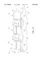
- FIG. 10illustrates a silicon oxide nitride oxide silicon (SONOS) memory devices 526 where charges can be ejected/stored in a dielectric layer to construct a volatile memory with a repressed memory state.
- the devices 526include a substrate 528, typically of monocrystalline silicon, which may or may not be lightly doped with a conductivity enhancing impurity, such as a p-type, to produce a bulk substrate well.
- An oxide-nitride-oxide layer 530is provided immediately adjacent bulk substrate 528 and would preferably constitute the typical ONO construction for a SONOS cell, such as SiO 2 /Si 3 N 4 /SiO 2 .
- a polysilicon gate layer 532is provided immediately adjacent ONO layer 530.
- An oxide layer 34 (e.g., SiO 2 ) and a nitride layer 536are provided outwardly of layer 532.
- LDDlightly-doped-drain
- a layer of nitrideis deposited and anisotropically etched to produce spacers 546 about gates 538 and 540. Subsequently, further doping is conducted between adjacent gates 538 and 540 with a conductivity enhancing impurity of the first conductivity type at a sufficient dose to form source/drain region 548, which is hereinafter termed as a source/drain interconnecting region. Such a region is provided to a greater dose and depth than the doping to produce LDD diffusion region 544, as would be conventional and known by people of skill in the art. Conventional diffusion regions 544 and 548 are illustrated. SONOS memory devices are described in U.S. Pat. No. 5,424,569 to Prall, which is hereby incorporated by reference.
Landscapes
- Dram (AREA)
Abstract
Description
Claims (83)
Priority Applications (1)
| Application Number | Priority Date | Filing Date | Title |
|---|---|---|---|
| US09/362,909US6141248A (en) | 1999-07-29 | 1999-07-29 | DRAM and SRAM memory cells with repressed memory |
Applications Claiming Priority (1)
| Application Number | Priority Date | Filing Date | Title |
|---|---|---|---|
| US09/362,909US6141248A (en) | 1999-07-29 | 1999-07-29 | DRAM and SRAM memory cells with repressed memory |
Publications (1)
| Publication Number | Publication Date |
|---|---|
| US6141248Atrue US6141248A (en) | 2000-10-31 |
Family
ID=23428005
Family Applications (1)
| Application Number | Title | Priority Date | Filing Date |
|---|---|---|---|
| US09/362,909Expired - LifetimeUS6141248A (en) | 1999-07-29 | 1999-07-29 | DRAM and SRAM memory cells with repressed memory |
Country Status (1)
| Country | Link |
|---|---|
| US (1) | US6141248A (en) |
Cited By (70)
| Publication number | Priority date | Publication date | Assignee | Title |
|---|---|---|---|---|
| US6331947B1 (en)* | 1999-10-04 | 2001-12-18 | U.S. Philips Corporation | Non-volatile MOS RAM cell with capacitor-isolated nodes that are radiation accessible for rendering a non-permanent programmed information in the cell a non-volatile one |
| US20020176313A1 (en)* | 1999-02-26 | 2002-11-28 | Micron Technology, Inc. | Dram technology compatible processor/memory chips |
| US6529407B2 (en)* | 2000-06-14 | 2003-03-04 | Hitachi, Ltd. | Semiconductor device with improved latch arrangement |
| US20030048666A1 (en)* | 2001-08-30 | 2003-03-13 | Micron Technology, Inc. | Graded composition metal oxide tunnel barrier interpoly insulators |
| US20040029322A1 (en)* | 2002-08-08 | 2004-02-12 | Prall Kirk D. | Method of forming a memory transistor comprising a Schottky contact |
| US6754108B2 (en)* | 2001-08-30 | 2004-06-22 | Micron Technology, Inc. | DRAM cells with repressed floating gate memory, low tunnel barrier interpoly insulators |
| US20040136228A1 (en)* | 2002-11-20 | 2004-07-15 | Giovanni Campardo | Semiconductor memory with embedded dram |
| US20040151029A1 (en)* | 1999-08-26 | 2004-08-05 | Micron Technology, Inc. | Programmable memory cell using charge trapping in a gate oxide |
| US20050023602A1 (en)* | 2001-08-30 | 2005-02-03 | Micron Technology, Inc. | Programmable array logic or memory with p-channel devices and asymmetrical tunnel barriers |
| US20050023595A1 (en)* | 2001-08-30 | 2005-02-03 | Micron Technology, Inc. | Programmable array logic or memory devices with asymmetrical tunnel barriers |
| US20050047194A1 (en)* | 2003-08-29 | 2005-03-03 | Jin-Hong Ahn | Non-volatile dynamic random access memory |
| JP2005191506A (en)* | 2003-12-24 | 2005-07-14 | Genusion:Kk | Nonvolatile memory, semiconductor integrated circuit device, and semiconductor device |
| US6956772B2 (en) | 2001-02-13 | 2005-10-18 | Micron Technology, Inc. | Programmable fuse and antifuse and method thereof |
| US6963103B2 (en)* | 2001-08-30 | 2005-11-08 | Micron Technology, Inc. | SRAM cells with repressed floating gate memory, low tunnel barrier interpoly insulators |
| US20060002192A1 (en)* | 2001-08-30 | 2006-01-05 | Micron Technology | Integrated circuit memory device and method |
| US20060044870A1 (en)* | 2004-08-27 | 2006-03-02 | Micron Technology, Inc. | Integrated DRAM-NVRAM multi-level memory |
| US7068544B2 (en) | 2001-08-30 | 2006-06-27 | Micron Technology, Inc. | Flash memory with low tunnel barrier interpoly insulators |
| US7075829B2 (en) | 2001-08-30 | 2006-07-11 | Micron Technology, Inc. | Programmable memory address and decode circuits with low tunnel barrier interpoly insulators |
| US7074673B2 (en) | 2001-08-30 | 2006-07-11 | Micron Technology, Inc. | Service programmable logic arrays with low tunnel barrier interpoly insulators |
| US20060170032A1 (en)* | 2001-08-30 | 2006-08-03 | Micron Technology, Inc. | Scalable Flash/NV structures and devices with extended endurance |
| US7221586B2 (en) | 2002-07-08 | 2007-05-22 | Micron Technology, Inc. | Memory utilizing oxide nanolaminates |
| US7301194B1 (en) | 2004-11-15 | 2007-11-27 | Xilinx, Inc. | Shrinkable and highly coupled double poly EEPROM with inverter |
| US7301811B1 (en)* | 2004-11-15 | 2007-11-27 | Xilinx, Inc. | Cost efficient nonvolatile SRAM cell |
| US7446368B2 (en) | 2001-08-30 | 2008-11-04 | Micron Technology, Inc. | Deposition of metal oxide and/or low asymmetrical tunnel barrier interpoly insulators |
| US20090168521A1 (en)* | 2007-12-31 | 2009-07-02 | Simtek | 5T high density NVDRAM cell |
| US20090168519A1 (en)* | 2007-12-31 | 2009-07-02 | Simtek | Architecture of a nvDRAM array and its sense regime |
| US20090168520A1 (en)* | 2007-12-31 | 2009-07-02 | Simtek | 3T high density NVDRAM cell |
| US20090316492A1 (en)* | 2007-11-29 | 2009-12-24 | Yuniarto Widjaja | Memory cells, memory cell arrays, methods of using and methods of making |
| US20100034041A1 (en)* | 2008-08-05 | 2010-02-11 | Yuniarto Widjaja | Method of operating semiconductor memory device with floating body transistor using silicon controlled rectifier principle |
| US20100046287A1 (en)* | 2008-08-22 | 2010-02-25 | Yuniarto Widjaja | Semiconductor memory having both volatile and non-volatile functionality including resistance change material and method of operating |
| US20100238728A1 (en)* | 2008-02-12 | 2010-09-23 | Chip Memory Technology, Inc. | Method and apparatus of operating a non-volatile DRAM |
| US20100246264A1 (en)* | 2006-11-29 | 2010-09-30 | Yuniarto Widjaja | Semiconductor memory having both volatile and non-volatile functionality and method of operating |
| US20100246277A1 (en)* | 2007-11-29 | 2010-09-30 | Yuniarto Widjaja | Method of maintaining the state of semiconductor memory having electrically floating body transistor |
| US20110032756A1 (en)* | 2007-11-29 | 2011-02-10 | Yuniarto Widjaja | Compact Semiconductor Memory Device Having Reduced Number of Contacts, Methods of Operating and Methods of Making |
| US20110042736A1 (en)* | 2007-10-24 | 2011-02-24 | Yuniarto Widjaja | Semiconductor memory having both volatile and non-volatile functionality and method of operating |
| US8110469B2 (en) | 2005-08-30 | 2012-02-07 | Micron Technology, Inc. | Graded dielectric layers |
| US8130548B2 (en) | 2007-11-29 | 2012-03-06 | Zeno Semiconductor, Inc. | Semiconductor memory having electrically floating body transistor |
| US8174886B2 (en) | 2007-11-29 | 2012-05-08 | Zeno Semiconductor, Inc. | Semiconductor memory having electrically floating body transistor |
| US8194471B2 (en) | 2010-10-04 | 2012-06-05 | Zeno Semiconductor, Inc. | Semiconductor memory device having an electrically floating body transistor |
| US8264875B2 (en) | 2010-10-04 | 2012-09-11 | Zeno Semiconducor, Inc. | Semiconductor memory device having an electrically floating body transistor |
| US8501563B2 (en) | 2005-07-20 | 2013-08-06 | Micron Technology, Inc. | Devices with nanocrystals and methods of formation |
| US8582359B2 (en) | 2010-11-16 | 2013-11-12 | Zeno Semiconductor, Inc. | Dual-port semiconductor memory and first-in first-out (FIFO) memory having electrically floating body transistor |
| US8923052B2 (en) | 2008-04-08 | 2014-12-30 | Zeno Semiconductor, Inc. | Semiconductor memory having volatile and multi-bit, non-volatile functionality and methods of operating |
| US8957458B2 (en) | 2011-03-24 | 2015-02-17 | Zeno Semiconductor, Inc. | Asymmetric semiconductor memory device having electrically floating body transistor |
| US9025358B2 (en) | 2011-10-13 | 2015-05-05 | Zeno Semiconductor Inc | Semiconductor memory having both volatile and non-volatile functionality comprising resistive change material and method of operating |
| US9029922B2 (en) | 2013-03-09 | 2015-05-12 | Zeno Semiconductor, Inc. | Memory device comprising electrically floating body transistor |
| US9153309B2 (en) | 2010-02-07 | 2015-10-06 | Zeno Semiconductor Inc. | Semiconductor memory device having electrically floating body transistor, semiconductor memory device having both volatile and non-volatile functionality and method or operating |
| US9208880B2 (en) | 2013-01-14 | 2015-12-08 | Zeno Semiconductor, Inc. | Content addressable memory device having electrically floating body transistor |
| US9230651B2 (en) | 2012-04-08 | 2016-01-05 | Zeno Semiconductor, Inc. | Memory device having electrically floating body transitor |
| US9275723B2 (en) | 2013-04-10 | 2016-03-01 | Zeno Semiconductor, Inc. | Scalable floating body memory cell for memory compilers and method of using floating body memories with memory compilers |
| US9281022B2 (en) | 2013-07-10 | 2016-03-08 | Zeno Semiconductor, Inc. | Systems and methods for reducing standby power in floating body memory devices |
| US9368625B2 (en) | 2013-05-01 | 2016-06-14 | Zeno Semiconductor, Inc. | NAND string utilizing floating body memory cell |
| US9391079B2 (en) | 2007-11-29 | 2016-07-12 | Zeno Semiconductor, Inc. | Compact semiconductor memory device having reduced number of contacts, methods of operating and methods of making |
| US9496053B2 (en) | 2014-08-15 | 2016-11-15 | Zeno Semiconductor, Inc. | Memory device comprising electrically floating body transistor |
| US9548119B2 (en) | 2014-01-15 | 2017-01-17 | Zeno Semiconductor, Inc | Memory device comprising an electrically floating body transistor |
| US9601493B2 (en) | 2006-11-29 | 2017-03-21 | Zeno Semiconductor, Inc | Compact semiconductor memory device having reduced number of contacts, methods of operating and methods of making |
| US9742403B2 (en) | 2013-04-02 | 2017-08-22 | Hewlett Packard Enterprise Development Lp | State-retaining logic cell |
| US9922981B2 (en) | 2010-03-02 | 2018-03-20 | Zeno Semiconductor, Inc. | Compact semiconductor memory device having reduced number of contacts, methods of operating and methods of making |
| US10079301B2 (en) | 2016-11-01 | 2018-09-18 | Zeno Semiconductor, Inc. | Memory device comprising an electrically floating body transistor and methods of using |
| USRE47381E1 (en) | 2008-09-03 | 2019-05-07 | Zeno Semiconductor, Inc. | Forming semiconductor cells with regions of varying conductivity |
| US10340276B2 (en) | 2010-03-02 | 2019-07-02 | Zeno Semiconductor, Inc. | Method of maintaining the state of semiconductor memory having electrically floating body transistor |
| US10403361B2 (en) | 2007-11-29 | 2019-09-03 | Zeno Semiconductor, Inc. | Memory cells, memory cell arrays, methods of using and methods of making |
| US10461084B2 (en) | 2010-03-02 | 2019-10-29 | Zeno Semiconductor, Inc. | Compact semiconductor memory device having reduced number of contacts, methods of operating and methods of making |
| US10553683B2 (en) | 2015-04-29 | 2020-02-04 | Zeno Semiconductor, Inc. | MOSFET and memory cell having improved drain current through back bias application |
| US11201215B2 (en) | 2015-04-29 | 2021-12-14 | Zeno Semiconductor, Inc. | MOSFET and memory cell having improved drain current through back bias application |
| US11404419B2 (en) | 2018-04-18 | 2022-08-02 | Zeno Semiconductor, Inc. | Memory device comprising an electrically floating body transistor |
| US11600663B2 (en) | 2019-01-11 | 2023-03-07 | Zeno Semiconductor, Inc. | Memory cell and memory array select transistor |
| US11908899B2 (en) | 2009-02-20 | 2024-02-20 | Zeno Semiconductor, Inc. | MOSFET and memory cell having improved drain current through back bias application |
| US11974425B2 (en) | 2012-02-16 | 2024-04-30 | Zeno Semiconductor, Inc. | Memory cell comprising first and second transistors and methods of operating |
| US12439611B2 (en) | 2019-03-12 | 2025-10-07 | Zeno Semiconductor, Inc. | Memory cell and memory array select transistor |
Citations (21)
| Publication number | Priority date | Publication date | Assignee | Title |
|---|---|---|---|---|
| US4271487A (en)* | 1979-11-13 | 1981-06-02 | Ncr Corporation | Static volatile/non-volatile ram cell |
| US4333166A (en)* | 1979-12-10 | 1982-06-01 | Hughes Aircraft Company | Semiconductor memory circuits |
| US4760556A (en)* | 1985-09-25 | 1988-07-26 | Mitsubishi Denki Kabushiki Kaisha | Nonvolatile semiconductor memory device |
| US5042011A (en)* | 1989-05-22 | 1991-08-20 | Micron Technology, Inc. | Sense amplifier pulldown device with tailored edge input |
| US5111427A (en)* | 1988-06-01 | 1992-05-05 | Mitsubishi Denki Kabushiki Kaisha | Nonvolatile content-addressable memory and operating method therefor |
| US5153853A (en)* | 1990-09-20 | 1992-10-06 | Sharp Kabushiki Kaisha | Method and apparatus for measuring EEPROM threshold voltages in a nonvolatile DRAM memory device |
| US5280205A (en)* | 1992-04-16 | 1994-01-18 | Micron Technology, Inc. | Fast sense amplifier |
| US5399516A (en)* | 1992-03-12 | 1995-03-21 | International Business Machines Corporation | Method of making shadow RAM cell having a shallow trench EEPROM |
| US5418739A (en)* | 1993-01-28 | 1995-05-23 | Oki Electric Industry Co., Ltd. | Semiconductor memory device |
| US5424569A (en)* | 1994-05-05 | 1995-06-13 | Micron Technology, Inc. | Array of non-volatile sonos memory cells |
| US5488587A (en)* | 1993-10-20 | 1996-01-30 | Sharp Kabushiki Kaisha | Non-volatile dynamic random access memory |
| US5497494A (en)* | 1993-07-23 | 1996-03-05 | International Business Machines Corporation | Method for saving and restoring the state of a CPU executing code in protected mode |
| US5619642A (en)* | 1994-12-23 | 1997-04-08 | Emc Corporation | Fault tolerant memory system which utilizes data from a shadow memory device upon the detection of erroneous data in a main memory device |
| US5627785A (en)* | 1996-03-15 | 1997-05-06 | Micron Technology, Inc. | Memory device with a sense amplifier |
| US5796670A (en)* | 1996-11-07 | 1998-08-18 | Ramax Semiconductor, Inc. | Nonvolatile dynamic random access memory device |
| US5801401A (en)* | 1997-01-29 | 1998-09-01 | Micron Technology, Inc. | Flash memory with microcrystalline silicon carbide film floating gate |
| US5852306A (en)* | 1997-01-29 | 1998-12-22 | Micron Technology, Inc. | Flash memory with nanocrystalline silicon film floating gate |
| US5870327A (en)* | 1996-07-19 | 1999-02-09 | Xilinx, Inc. | Mixed mode RAM/ROM cell using antifuses |
| US5880991A (en)* | 1997-04-14 | 1999-03-09 | International Business Machines Corporation | Structure for low cost mixed memory integration, new NVRAM structure, and process for forming the mixed memory and NVRAM structure |
| US5986932A (en)* | 1997-06-30 | 1999-11-16 | Cypress Semiconductor Corp. | Non-volatile static random access memory and methods for using same |
| US6009011A (en)* | 1996-12-27 | 1999-12-28 | Sharp Kabushiki Kaisha | Non-volatile memory and method for operating the same |
- 1999
- 1999-07-29USUS09/362,909patent/US6141248A/ennot_activeExpired - Lifetime
Patent Citations (21)
| Publication number | Priority date | Publication date | Assignee | Title |
|---|---|---|---|---|
| US4271487A (en)* | 1979-11-13 | 1981-06-02 | Ncr Corporation | Static volatile/non-volatile ram cell |
| US4333166A (en)* | 1979-12-10 | 1982-06-01 | Hughes Aircraft Company | Semiconductor memory circuits |
| US4760556A (en)* | 1985-09-25 | 1988-07-26 | Mitsubishi Denki Kabushiki Kaisha | Nonvolatile semiconductor memory device |
| US5111427A (en)* | 1988-06-01 | 1992-05-05 | Mitsubishi Denki Kabushiki Kaisha | Nonvolatile content-addressable memory and operating method therefor |
| US5042011A (en)* | 1989-05-22 | 1991-08-20 | Micron Technology, Inc. | Sense amplifier pulldown device with tailored edge input |
| US5153853A (en)* | 1990-09-20 | 1992-10-06 | Sharp Kabushiki Kaisha | Method and apparatus for measuring EEPROM threshold voltages in a nonvolatile DRAM memory device |
| US5399516A (en)* | 1992-03-12 | 1995-03-21 | International Business Machines Corporation | Method of making shadow RAM cell having a shallow trench EEPROM |
| US5280205A (en)* | 1992-04-16 | 1994-01-18 | Micron Technology, Inc. | Fast sense amplifier |
| US5418739A (en)* | 1993-01-28 | 1995-05-23 | Oki Electric Industry Co., Ltd. | Semiconductor memory device |
| US5497494A (en)* | 1993-07-23 | 1996-03-05 | International Business Machines Corporation | Method for saving and restoring the state of a CPU executing code in protected mode |
| US5488587A (en)* | 1993-10-20 | 1996-01-30 | Sharp Kabushiki Kaisha | Non-volatile dynamic random access memory |
| US5424569A (en)* | 1994-05-05 | 1995-06-13 | Micron Technology, Inc. | Array of non-volatile sonos memory cells |
| US5619642A (en)* | 1994-12-23 | 1997-04-08 | Emc Corporation | Fault tolerant memory system which utilizes data from a shadow memory device upon the detection of erroneous data in a main memory device |
| US5627785A (en)* | 1996-03-15 | 1997-05-06 | Micron Technology, Inc. | Memory device with a sense amplifier |
| US5870327A (en)* | 1996-07-19 | 1999-02-09 | Xilinx, Inc. | Mixed mode RAM/ROM cell using antifuses |
| US5796670A (en)* | 1996-11-07 | 1998-08-18 | Ramax Semiconductor, Inc. | Nonvolatile dynamic random access memory device |
| US6009011A (en)* | 1996-12-27 | 1999-12-28 | Sharp Kabushiki Kaisha | Non-volatile memory and method for operating the same |
| US5801401A (en)* | 1997-01-29 | 1998-09-01 | Micron Technology, Inc. | Flash memory with microcrystalline silicon carbide film floating gate |
| US5852306A (en)* | 1997-01-29 | 1998-12-22 | Micron Technology, Inc. | Flash memory with nanocrystalline silicon film floating gate |
| US5880991A (en)* | 1997-04-14 | 1999-03-09 | International Business Machines Corporation | Structure for low cost mixed memory integration, new NVRAM structure, and process for forming the mixed memory and NVRAM structure |
| US5986932A (en)* | 1997-06-30 | 1999-11-16 | Cypress Semiconductor Corp. | Non-volatile static random access memory and methods for using same |
Non-Patent Citations (2)
| Title |
|---|
| Dipert et al., "Flash Memory Goes Mainstream," IEEE SPECTRUM, Oct. 1993/vol. 30/Nov. 10, pp. 48-52. |
| Dipert et al., Flash Memory Goes Mainstream, IEEE SPECTRUM, Oct. 1993/vol. 30/Nov. 10, pp. 48 52.* |
Cited By (343)
| Publication number | Priority date | Publication date | Assignee | Title |
|---|---|---|---|---|
| US20020176313A1 (en)* | 1999-02-26 | 2002-11-28 | Micron Technology, Inc. | Dram technology compatible processor/memory chips |
| US20020176293A1 (en)* | 1999-02-26 | 2002-11-28 | Micron Technology, Inc. | DRAM technology compatible processor/memory chips |
| US6741519B2 (en) | 1999-02-26 | 2004-05-25 | Micron Technology, Inc. | DRAM technology compatible processor/memory chips |
| US6809985B2 (en) | 1999-02-26 | 2004-10-26 | Micron Technology, Inc. | DRAM technology compatible processor/memory chips |
| US6924194B2 (en) | 1999-02-26 | 2005-08-02 | Micron Technology, Inc. | DRAM technology compatible processor/memory chips |
| US7023040B2 (en) | 1999-02-26 | 2006-04-04 | Micron Technology, Inc. | DRAM technology compatible processor/memory chips |
| US20060124981A1 (en)* | 1999-02-26 | 2006-06-15 | Micron Technology, Inc. | DRAM technology compatible processor/memory chips |
| US20040151029A1 (en)* | 1999-08-26 | 2004-08-05 | Micron Technology, Inc. | Programmable memory cell using charge trapping in a gate oxide |
| US6909635B2 (en) | 1999-08-26 | 2005-06-21 | Micron Technology, Inc. | Programmable memory cell using charge trapping in a gate oxide |
| US6331947B1 (en)* | 1999-10-04 | 2001-12-18 | U.S. Philips Corporation | Non-volatile MOS RAM cell with capacitor-isolated nodes that are radiation accessible for rendering a non-permanent programmed information in the cell a non-volatile one |
| US6724657B2 (en) | 2000-06-14 | 2004-04-20 | Renesas Technology Corp. | Semiconductor device with improved latch arrangement |
| US20030067822A1 (en)* | 2000-06-14 | 2003-04-10 | Shoji Shukuri | Semiconductor device with improved latch arrangement |
| US6529407B2 (en)* | 2000-06-14 | 2003-03-04 | Hitachi, Ltd. | Semiconductor device with improved latch arrangement |
| US7177193B2 (en) | 2001-02-13 | 2007-02-13 | Micron Technology, Inc. | Programmable fuse and antifuse and method therefor |
| US20060002187A1 (en)* | 2001-02-13 | 2006-01-05 | Micron Technology, Inc. | Programmable fuse and antifuse and method therefor |
| US6956772B2 (en) | 2001-02-13 | 2005-10-18 | Micron Technology, Inc. | Programmable fuse and antifuse and method thereof |
| US7068544B2 (en) | 2001-08-30 | 2006-06-27 | Micron Technology, Inc. | Flash memory with low tunnel barrier interpoly insulators |
| US7187587B2 (en) | 2001-08-30 | 2007-03-06 | Micron Technology, Inc. | Programmable memory address and decode circuits with low tunnel barrier interpoly insulators |
| US20050023595A1 (en)* | 2001-08-30 | 2005-02-03 | Micron Technology, Inc. | Programmable array logic or memory devices with asymmetrical tunnel barriers |
| US7443715B2 (en) | 2001-08-30 | 2008-10-28 | Micron Technology, Inc. | SRAM cells with repressed floating gate memory, low tunnel barrier interpoly insulators |
| US7446368B2 (en) | 2001-08-30 | 2008-11-04 | Micron Technology, Inc. | Deposition of metal oxide and/or low asymmetrical tunnel barrier interpoly insulators |
| US7400012B2 (en) | 2001-08-30 | 2008-07-15 | Micron Technology, Inc. | Scalable Flash/NV structures and devices with extended endurance |
| US7391072B2 (en) | 2001-08-30 | 2008-06-24 | Micron Technology, Inc. | Programmable array logic or memory with p-channel devices and asymmetrical tunnel barriers |
| US20040190342A1 (en)* | 2001-08-30 | 2004-09-30 | Micron Technology, Inc. | DRAM cells with repressed floating gate memory, low tunnel barrier interpoly insulators |
| US6952032B2 (en) | 2001-08-30 | 2005-10-04 | Micron Technology, Inc. | Programmable array logic or memory devices with asymmetrical tunnel barriers |
| US7465983B2 (en) | 2001-08-30 | 2008-12-16 | Micron Technology, Inc. | Low tunnel barrier insulators |
| US6958937B2 (en) | 2001-08-30 | 2005-10-25 | Micron Technology Inc. | DRAM cells with repressed floating gate memory, low tunnel barrier interpoly insulators |
| US6963103B2 (en)* | 2001-08-30 | 2005-11-08 | Micron Technology, Inc. | SRAM cells with repressed floating gate memory, low tunnel barrier interpoly insulators |
| US7372097B2 (en) | 2001-08-30 | 2008-05-13 | Micron Technology, Inc. | Programmable array logic or memory with p-channel devices and asymmetrical tunnel barriers |
| US20060002192A1 (en)* | 2001-08-30 | 2006-01-05 | Micron Technology | Integrated circuit memory device and method |
| US7372096B2 (en) | 2001-08-30 | 2008-05-13 | Micron Technology, Inc. | Programmable array logic or memory with p-channel devices and asymmetrical tunnel barriers |
| US7473956B2 (en) | 2001-08-30 | 2009-01-06 | Micron Technology, Inc. | Atomic layer deposition of metal oxide and/or low assymmetrical tunnel barrier interpoly insulators |
| US7027328B2 (en) | 2001-08-30 | 2006-04-11 | Micron Technology, Inc. | Integrated circuit memory device and method |
| US7476925B2 (en) | 2001-08-30 | 2009-01-13 | Micron Technology, Inc. | Atomic layer deposition of metal oxide and/or low asymmetrical tunnel barrier interploy insulators |
| US7042043B2 (en) | 2001-08-30 | 2006-05-09 | Micron Technology, Inc. | Programmable array logic or memory devices with asymmetrical tunnel barriers |
| US7504687B2 (en) | 2001-08-30 | 2009-03-17 | Micron Technology, Inc. | Atomic layer deposition of metal oxide and/or low asymmetrical tunnel barrier interpoly insulators |
| US6754108B2 (en)* | 2001-08-30 | 2004-06-22 | Micron Technology, Inc. | DRAM cells with repressed floating gate memory, low tunnel barrier interpoly insulators |
| US7274067B2 (en) | 2001-08-30 | 2007-09-25 | Micron Technology, Inc. | Service programmable logic arrays with low tunnel barrier interpoly insulators |
| US7759724B2 (en)* | 2001-08-30 | 2010-07-20 | Micron Technology, Inc. | Memory cells having gate structure with multiple gates and multiple materials between the gates |
| US7750395B2 (en) | 2001-08-30 | 2010-07-06 | Micron Technology, Inc. | Scalable Flash/NV structures and devices with extended endurance |
| US20050023602A1 (en)* | 2001-08-30 | 2005-02-03 | Micron Technology, Inc. | Programmable array logic or memory with p-channel devices and asymmetrical tunnel barriers |
| US7075829B2 (en) | 2001-08-30 | 2006-07-11 | Micron Technology, Inc. | Programmable memory address and decode circuits with low tunnel barrier interpoly insulators |
| US7074673B2 (en) | 2001-08-30 | 2006-07-11 | Micron Technology, Inc. | Service programmable logic arrays with low tunnel barrier interpoly insulators |
| US20030048666A1 (en)* | 2001-08-30 | 2003-03-13 | Micron Technology, Inc. | Graded composition metal oxide tunnel barrier interpoly insulators |
| US7166886B2 (en) | 2001-08-30 | 2007-01-23 | Micron Technology, Inc. | DRAM cells with repressed floating gate memory, low tunnel barrier interpoly insulators |
| US20060170032A1 (en)* | 2001-08-30 | 2006-08-03 | Micron Technology, Inc. | Scalable Flash/NV structures and devices with extended endurance |
| US7087954B2 (en) | 2001-08-30 | 2006-08-08 | Micron Technology, Inc. | In service programmable logic arrays with low tunnel barrier interpoly insulators |
| US7545674B2 (en) | 2001-08-30 | 2009-06-09 | Micron Technology, Inc. | Flash memory with low tunnel barrier interpoly insulators |
| US7508025B2 (en) | 2001-08-30 | 2009-03-24 | Micron Technology, Inc. | Atomic layer deposition of metal oxide and/or low asymmetrical tunnel barrier interpoly insulators |
| US7112841B2 (en) | 2001-08-30 | 2006-09-26 | Micron Technology, Inc. | Graded composition metal oxide tunnel barrier interpoly insulators |
| US7126183B2 (en) | 2001-08-30 | 2006-10-24 | Micron Technology, Inc. | Programmable array logic or memory with p-channel devices and asymmetrical tunnel barriers |
| US7132711B2 (en) | 2001-08-30 | 2006-11-07 | Micron Technology, Inc. | Programmable array logic or memory with p-channel devices and asymmetrical tunnel barriers |
| US7136302B2 (en) | 2001-08-30 | 2006-11-14 | Micron Technology, Inc. | Integrated circuit memory device and method |
| US7135734B2 (en) | 2001-08-30 | 2006-11-14 | Micron Technology, Inc. | Graded composition metal oxide tunnel barrier interpoly insulators |
| US20060263981A1 (en)* | 2001-08-30 | 2006-11-23 | Micron Technology, Inc. | DRAM cells with repressed floating gate memory, low tunnel barrier interpoly insulators |
| US20060274580A1 (en)* | 2001-08-30 | 2006-12-07 | Micron Technology, Inc. | DRAM cells with repressed floating gate memory, low tunnel barrier interpoly insulators |
| US7221586B2 (en) | 2002-07-08 | 2007-05-22 | Micron Technology, Inc. | Memory utilizing oxide nanolaminates |
| US7433237B2 (en) | 2002-07-08 | 2008-10-07 | Micron Technology, Inc. | Memory utilizing oxide nanolaminates |
| US7728626B2 (en) | 2002-07-08 | 2010-06-01 | Micron Technology, Inc. | Memory utilizing oxide nanolaminates |
| US8228725B2 (en) | 2002-07-08 | 2012-07-24 | Micron Technology, Inc. | Memory utilizing oxide nanolaminates |
| US6791140B2 (en)* | 2002-08-08 | 2004-09-14 | Micron Technology, Inc. | Memory transistor structure |
| US20070111443A1 (en)* | 2002-08-08 | 2007-05-17 | Prall Kirk D | Memory transistor and methods |
| US7745283B2 (en) | 2002-08-08 | 2010-06-29 | Micron Technology, Inc. | Method of fabricating memory transistor |
| US7651911B2 (en) | 2002-08-08 | 2010-01-26 | Micron Technology, Inc. | Memory transistor and methods |
| US20040029322A1 (en)* | 2002-08-08 | 2004-02-12 | Prall Kirk D. | Method of forming a memory transistor comprising a Schottky contact |
| US20040029370A1 (en)* | 2002-08-08 | 2004-02-12 | Prall Kirk D. | Memory transistor and methods |
| US6835619B2 (en)* | 2002-08-08 | 2004-12-28 | Micron Technology, Inc. | Method of forming a memory transistor comprising a Schottky contact |
| US20050122787A1 (en)* | 2002-08-08 | 2005-06-09 | Prall Kirk D. | Memory transistor and methods |
| US7027317B2 (en)* | 2002-11-20 | 2006-04-11 | Stmicroelectronics, S.R.L. | Semiconductor memory with embedded DRAM |
| US20040136228A1 (en)* | 2002-11-20 | 2004-07-15 | Giovanni Campardo | Semiconductor memory with embedded dram |
| US7099181B2 (en)* | 2003-08-29 | 2006-08-29 | Hynix Semiconductor Inc. | Non-volatile dynamic random access memory |
| US20050047194A1 (en)* | 2003-08-29 | 2005-03-03 | Jin-Hong Ahn | Non-volatile dynamic random access memory |
| JP2005191506A (en)* | 2003-12-24 | 2005-07-14 | Genusion:Kk | Nonvolatile memory, semiconductor integrated circuit device, and semiconductor device |
| US20060146605A1 (en)* | 2004-08-27 | 2006-07-06 | Micron Technology, Inc. | Integrated DRAM-NVRAM multi-level memory |
| US20060146594A1 (en)* | 2004-08-27 | 2006-07-06 | Micron Technology, Inc. | Integrated DRAM-NVRAM multi-level memory |
| US7403416B2 (en) | 2004-08-27 | 2008-07-22 | Micron Technology, Inc. | Integrated DRAM-NVRAM multi-level memory |
| US7403419B2 (en) | 2004-08-27 | 2008-07-22 | Micron Technology, Inc. | Integrated DRAM-NVRAM multi-level memory |
| US7457159B2 (en) | 2004-08-27 | 2008-11-25 | Micron Technology, Inc. | Integrated DRAM-NVRAM multi-level memory |
| US7459740B2 (en) | 2004-08-27 | 2008-12-02 | Micron Technology, Inc. | Integrated DRAM-NVRAM multi-level memory |
| US7379336B2 (en) | 2004-08-27 | 2008-05-27 | Micron Technology, Inc. | Integrated DRAM-NVRAM multi-level memory |
| US7349252B2 (en) | 2004-08-27 | 2008-03-25 | Micron Technology, Inc. | Integrated DRAM-NVRAM multi-level memory |
| US20060145246A1 (en)* | 2004-08-27 | 2006-07-06 | Micron Technology, Inc. | Integrated DRAM-NVRAM multi-level memory |
| US20060146606A1 (en)* | 2004-08-27 | 2006-07-06 | Micron Technology, Inc. | Integrated DRAM-NVRAM multi-level memory |
| US7158410B2 (en) | 2004-08-27 | 2007-01-02 | Micron Technology, Inc. | Integrated DRAM-NVRAM multi-level memory |
| US20060176726A1 (en)* | 2004-08-27 | 2006-08-10 | Micron Technology, Inc. | Integrated DRAM-NVRAM multi-level memory |
| US7417893B2 (en) | 2004-08-27 | 2008-08-26 | Micron Technology, Inc. | Integrated DRAM-NVRAM multi-level memory |
| US20060044870A1 (en)* | 2004-08-27 | 2006-03-02 | Micron Technology, Inc. | Integrated DRAM-NVRAM multi-level memory |
| US20060152963A1 (en)* | 2004-08-27 | 2006-07-13 | Micron Technology, Inc. | Integrated DRAM-NVRAM multi-level memory |
| US20060152962A1 (en)* | 2004-08-27 | 2006-07-13 | Micron Technology, Inc. | Integrated DRAM-NVRAM multi-level memory |
| US7301811B1 (en)* | 2004-11-15 | 2007-11-27 | Xilinx, Inc. | Cost efficient nonvolatile SRAM cell |
| US7301194B1 (en) | 2004-11-15 | 2007-11-27 | Xilinx, Inc. | Shrinkable and highly coupled double poly EEPROM with inverter |
| US8501563B2 (en) | 2005-07-20 | 2013-08-06 | Micron Technology, Inc. | Devices with nanocrystals and methods of formation |
| US8921914B2 (en) | 2005-07-20 | 2014-12-30 | Micron Technology, Inc. | Devices with nanocrystals and methods of formation |
| US9627501B2 (en) | 2005-08-30 | 2017-04-18 | Micron Technology, Inc. | Graded dielectric structures |
| US8110469B2 (en) | 2005-08-30 | 2012-02-07 | Micron Technology, Inc. | Graded dielectric layers |
| US8951903B2 (en) | 2005-08-30 | 2015-02-10 | Micron Technology, Inc. | Graded dielectric structures |
| US9601493B2 (en) | 2006-11-29 | 2017-03-21 | Zeno Semiconductor, Inc | Compact semiconductor memory device having reduced number of contacts, methods of operating and methods of making |
| US8391066B2 (en) | 2006-11-29 | 2013-03-05 | Zeno Semiconductor, Inc. | Semiconductor memory having both volatile and non-volatile functionality and method of operating |
| US20100246264A1 (en)* | 2006-11-29 | 2010-09-30 | Yuniarto Widjaja | Semiconductor memory having both volatile and non-volatile functionality and method of operating |
| US8036033B2 (en)* | 2006-11-29 | 2011-10-11 | Z End Semiconductor, Inc. | Semiconductor memory having both volatile and non-volatile functionality and method of operating |
| US8570803B2 (en) | 2006-11-29 | 2013-10-29 | Zeno Semiconductor, Inc. | Semiconductor memory having both volatile and non-volatile functionality and method of operating |
| US20110042736A1 (en)* | 2007-10-24 | 2011-02-24 | Yuniarto Widjaja | Semiconductor memory having both volatile and non-volatile functionality and method of operating |
| US20110044110A1 (en)* | 2007-10-24 | 2011-02-24 | Yuniarto Widjaja | Semiconductor memory having both volatile and non-volatile functionality and method of operating |
| US10825520B2 (en) | 2007-10-24 | 2020-11-03 | Zeno Semiconductor, Inc. | Semiconductor memory having both volatile and non-volatile functionality and method of operating |
| US8787085B2 (en) | 2007-10-24 | 2014-07-22 | Zeno Semiconductor, Inc. | Semiconductor memory having both volatile and non-volatile functionality and method of operating |
| US9761311B2 (en) | 2007-10-24 | 2017-09-12 | Zeno Semiconductor, Inc. | Semiconductor memory having both volatile and non-volatile functionality |
| US9460790B2 (en) | 2007-10-24 | 2016-10-04 | Zeno Semiconductor, Inc. | Semiconductor memory having both volatile and non-volatile functionality and method of operating |
| US8472249B2 (en) | 2007-10-24 | 2013-06-25 | Zeno Semiconductor, Inc. | Semiconductor memory having both volatile and non-volatile functionality and method of operating |
| US9153333B2 (en) | 2007-10-24 | 2015-10-06 | Zeno Semiconductor, Inc. | Semiconductor memory having both volatile and non-volatile functionality and method of operating |
| US11488665B2 (en) | 2007-10-24 | 2022-11-01 | Zeno Semiconductor, Inc. | Semiconductor memory having both volatile and non-volatile functionality and method of operating |
| US8294193B2 (en) | 2007-10-24 | 2012-10-23 | Zeno Semiconductor, Inc. | Semiconductor memory having both volatile and non-volatile functionality and method of operating |
| US11862245B2 (en) | 2007-10-24 | 2024-01-02 | Zeno Semiconductor, Inc. | Semiconductor memory having both volatile and non-volatile functionality and method of operating |
| US10468102B2 (en) | 2007-10-24 | 2019-11-05 | Zeno Semiconductor, Inc | Semiconductor memory having both volatile and non-volatile functionality and method of operating |
| US8159878B2 (en) | 2007-10-24 | 2012-04-17 | Zeno Semiconductor, Inc. | Semiconductor memory having both volatile and non-volatile functionality and method of operating |
| US8194451B2 (en) | 2007-11-29 | 2012-06-05 | Zeno Semiconductor, Inc. | Memory cells, memory cell arrays, methods of using and methods of making |
| US9001581B2 (en) | 2007-11-29 | 2015-04-07 | Zeno Semiconductor Inc. | Compact semiconductor memory device having reduced number of contacts, methods of operating and methods of making |
| US8174886B2 (en) | 2007-11-29 | 2012-05-08 | Zeno Semiconductor, Inc. | Semiconductor memory having electrically floating body transistor |
| US8208302B2 (en) | 2007-11-29 | 2012-06-26 | Zeno Semiconductor, Inc. | Method of maintaining the state of semiconductor memory having electrically floating body transistor |
| US8130548B2 (en) | 2007-11-29 | 2012-03-06 | Zeno Semiconductor, Inc. | Semiconductor memory having electrically floating body transistor |
| US10242739B2 (en) | 2007-11-29 | 2019-03-26 | Zeno Semiconductor, Inc. | Memory cells, memory cell arrays, methods of using and methods of making |
| US9236382B2 (en) | 2007-11-29 | 2016-01-12 | Zeno Semiconductor, Inc. | Method of maintaining the state of semiconductor memory having electrically floating body transistor |
| US10109349B2 (en) | 2007-11-29 | 2018-10-23 | Zeno Semiconductors, Inc. | Memory cells, memory cell arrays, methods of using and methods of making |
| US8130547B2 (en) | 2007-11-29 | 2012-03-06 | Zeno Semiconductor, Inc. | Method of maintaining the state of semiconductor memory having electrically floating body transistor |
| US9391079B2 (en) | 2007-11-29 | 2016-07-12 | Zeno Semiconductor, Inc. | Compact semiconductor memory device having reduced number of contacts, methods of operating and methods of making |
| US9514803B2 (en) | 2007-11-29 | 2016-12-06 | Zeno Semiconductor, Inc. | Semiconductor memory having electrically floating body transistor |
| US9209188B2 (en) | 2007-11-29 | 2015-12-08 | Zeno Semiconductor, Inc. | Compact semiconductor memory device having reduced number of contacts, methods of operating and methods of making |
| US20090316492A1 (en)* | 2007-11-29 | 2009-12-24 | Yuniarto Widjaja | Memory cells, memory cell arrays, methods of using and methods of making |
| US9030872B2 (en) | 2007-11-29 | 2015-05-12 | Zeno Semiconductor, Inc. | Method of maintaining the state of semiconductor memory having electrically floating body transistor |
| US8514623B2 (en) | 2007-11-29 | 2013-08-20 | Zeno Semiconductor, Inc. | Method of maintaining the state of semiconductor memory having electrically floating body transistor |
| US8514622B2 (en) | 2007-11-29 | 2013-08-20 | Zeno Semiconductor, Inc. | Compact semiconductor memory device having reduced number of contacts, methods of operating and methods of making |
| US8531881B2 (en) | 2007-11-29 | 2013-09-10 | Zeno Semiconductor, Inc. | Memory cells, memory cell arrays, methods of using and methods of making |
| US10032776B2 (en) | 2007-11-29 | 2018-07-24 | Zeno Semiconductor, Inc. | Method of maintaining the state of semiconductor memory having electrically floating body transistor |
| US9978450B2 (en) | 2007-11-29 | 2018-05-22 | Zeno Semiconductor, Inc. | Memory cells, memory cell arrays, methods of using and methods of making |
| US9653467B2 (en) | 2007-11-29 | 2017-05-16 | Zeno Semiconductor, Inc. | Method of maintaining the state of semiconductor memory having electrically floating body transistor |
| US10403361B2 (en) | 2007-11-29 | 2019-09-03 | Zeno Semiconductor, Inc. | Memory cells, memory cell arrays, methods of using and methods of making |
| US8654583B2 (en) | 2007-11-29 | 2014-02-18 | Zeno Semiconductor, Inc. | Memory cells, memory cell arrays, methods of using and methods of making |
| US8711622B2 (en) | 2007-11-29 | 2014-04-29 | Zeno Semiconductor, Inc. | Compact semiconductor memory device having reduced number of contacts, methods of operating and methods of making |
| US9847131B2 (en) | 2007-11-29 | 2017-12-19 | Zeno Semiconductor, Inc. | Memory cells, memory cell arrays, methods of using and methods of making |
| US20110032756A1 (en)* | 2007-11-29 | 2011-02-10 | Yuniarto Widjaja | Compact Semiconductor Memory Device Having Reduced Number of Contacts, Methods of Operating and Methods of Making |
| US9793277B2 (en) | 2007-11-29 | 2017-10-17 | Zeno Semiconductor, Inc. | Method of maintaining the state of semiconductor memory having electrically floating body transistor |
| US20100246277A1 (en)* | 2007-11-29 | 2010-09-30 | Yuniarto Widjaja | Method of maintaining the state of semiconductor memory having electrically floating body transistor |
| US8995186B2 (en) | 2007-11-29 | 2015-03-31 | Zeno Semiconductors, Inc. | Memory cells, memory cell arrays, methods of using and methods of making |
| US9679648B2 (en) | 2007-11-29 | 2017-06-13 | Zeno Semiconductor, Inc. | Memory cells, memory cell arrays, methods of using and methods of making |
| US9715932B2 (en) | 2007-11-29 | 2017-07-25 | Zeno Semiconductor, Inc. | Memory cells, memory cell arrays, methods of using and methods of making |
| US8937834B2 (en) | 2007-11-29 | 2015-01-20 | Zeno Semiconductor, Inc. | Method of maintaining the state of semiconductor memory having electrically floating body transistor |
| WO2009088717A1 (en)* | 2007-12-31 | 2009-07-16 | Cypress Semiconductor Corporation | 5t high density nvdram cell |
| US20090168520A1 (en)* | 2007-12-31 | 2009-07-02 | Simtek | 3T high density NVDRAM cell |
| US20090168521A1 (en)* | 2007-12-31 | 2009-07-02 | Simtek | 5T high density NVDRAM cell |
| US20090168519A1 (en)* | 2007-12-31 | 2009-07-02 | Simtek | Architecture of a nvDRAM array and its sense regime |
| US8036032B2 (en)* | 2007-12-31 | 2011-10-11 | Cypress Semiconductor Corporation | 5T high density NVDRAM cell |
| US8064255B2 (en) | 2007-12-31 | 2011-11-22 | Cypress Semiconductor Corporation | Architecture of a nvDRAM array and its sense regime |
| US8488379B2 (en) | 2007-12-31 | 2013-07-16 | Cypress Semiconductor Corporation | 5T high density nvDRAM cell |
| US8059458B2 (en) | 2007-12-31 | 2011-11-15 | Cypress Semiconductor Corporation | 3T high density nvDRAM cell |
| US20100238728A1 (en)* | 2008-02-12 | 2010-09-23 | Chip Memory Technology, Inc. | Method and apparatus of operating a non-volatile DRAM |
| US8391078B2 (en)* | 2008-02-12 | 2013-03-05 | Chip Memory Technology, Inc. | Method and apparatus of operating a non-volatile DRAM |
| US9257179B2 (en) | 2008-04-08 | 2016-02-09 | Zeno Semiconductor, Inc. | Semiconductor memory having volatile and multi-bit non-volatile functionality and method of operating |
| US9646693B2 (en) | 2008-04-08 | 2017-05-09 | Zeno Semiconductor, Inc. | Semiconductor memory having volatile and multi-bit non-volatile functionality and method of operating |
| US10818354B2 (en) | 2008-04-08 | 2020-10-27 | Zeno Semiconductor, Inc. | Semiconductor memory having volatile and multi-bit non-volatile functionality and method of operating |
| US9928910B2 (en) | 2008-04-08 | 2018-03-27 | Zeno Semiconductor, Inc. | Semiconductor memory having volatile and multi-bit non-volatile functionality and method of operating |
| US8923052B2 (en) | 2008-04-08 | 2014-12-30 | Zeno Semiconductor, Inc. | Semiconductor memory having volatile and multi-bit, non-volatile functionality and methods of operating |
| US10210934B2 (en) | 2008-04-08 | 2019-02-19 | Zeno Semiconductor, Inc. | Semiconductor memory having volatile and multi-bit non-volatile functionality and method of operating |
| US9484082B2 (en) | 2008-08-05 | 2016-11-01 | Zeno Semiconductor, Inc. | Method of operating semiconductor memory device with floating body transistor using silicon controlled rectifier principle |
| US10211209B2 (en) | 2008-08-05 | 2019-02-19 | Zeno Semiconductor, Inc. | Method of operating semiconductor memory device with floating body transistor using silicon controlled rectifier principle |
| US12426238B2 (en) | 2008-08-05 | 2025-09-23 | Zeno Semiconductor, Inc. | Method of operating semiconductor memory device with floating body transistor using silicon controlled rectifier principle |
| US10644002B2 (en) | 2008-08-05 | 2020-05-05 | Zeno Semiconductor, Inc. | Method of operating semiconductor memory device with floating body transistor using silicon controlled rectifier principle |
| US8559257B2 (en) | 2008-08-05 | 2013-10-15 | Zeno Semiconductor, Inc. | Method of operating semiconductor memory device with floating body transistor using silicon controlled rectifier principle |
| US11404420B2 (en) | 2008-08-05 | 2022-08-02 | Zeno Semiconductor, Inc. | Method of operating semiconductor memory device with floating body transistor using silicon controlled rectifier principle |
| US9960166B2 (en) | 2008-08-05 | 2018-05-01 | Zeno Semiconductor, Inc. | Method of operating semiconductor memory device with floating body transisor using silicon controlled rectifier principle |
| US8077536B2 (en) | 2008-08-05 | 2011-12-13 | Zeno Semiconductor, Inc. | Method of operating semiconductor memory device with floating body transistor using silicon controlled rectifier principle |
| US9761589B2 (en) | 2008-08-05 | 2017-09-12 | Zeno Semiconductor, Inc. | Method of operating semiconductor memory device with floating body transistor using silicon controlled rectifier principle |
| US9230965B2 (en) | 2008-08-05 | 2016-01-05 | Zeno Semiconductor, Inc. | Method of operating semiconductor memory device with floating body transistor using silicon controlled rectifier principle |
| US8837247B2 (en) | 2008-08-05 | 2014-09-16 | Zeno Semiconductor, Inc. | Method of operating semiconductor memory device with floating body transistor using silicon controlled rectifier principle |
| US11785758B2 (en) | 2008-08-05 | 2023-10-10 | Zeno Semiconductor, Inc. | Method of operating semiconductor memory device with floating body transistor using silicon controlled rectifier principle |
| US10991698B2 (en) | 2008-08-05 | 2021-04-27 | Zeno Semiconductor, Inc. | Method of operating semiconductor memory device with floating body transistor using silicon controlled rectifier principle |
| US20100034041A1 (en)* | 2008-08-05 | 2010-02-11 | Yuniarto Widjaja | Method of operating semiconductor memory device with floating body transistor using silicon controlled rectifier principle |
| US8243499B2 (en) | 2008-08-22 | 2012-08-14 | Zeno Semiconductor, Inc. | Semiconductor memory having both volatile and non-volatile functionality including resistance change material and method of operating |
| US10032514B2 (en) | 2008-08-22 | 2018-07-24 | Zeno Semiconductor, Inc. | Semiconductor memory having both volatile and non-volatile functionality including resistance change material and method of operating |
| US20100046287A1 (en)* | 2008-08-22 | 2010-02-25 | Yuniarto Widjaja | Semiconductor memory having both volatile and non-volatile functionality including resistance change material and method of operating |
| US11727987B2 (en) | 2008-08-22 | 2023-08-15 | Zeno Semiconductor, Inc. | Semiconductor memory having both volatile and non-volatile functionality including resistance change material and method of operating |
| US8159868B2 (en) | 2008-08-22 | 2012-04-17 | Zeno Semiconductor, Inc. | Semiconductor memory having both volatile and non-volatile functionality including resistance change material and method of operating |
| US20110228591A1 (en)* | 2008-08-22 | 2011-09-22 | Yuniarto Widjaja | Semiconductor memory having both volatile and non-volatile functionality including resistance change material and method of operating |
| US11295813B2 (en) | 2008-08-22 | 2022-04-05 | Zeno Semiconductor Inc. | Semiconductor memory having both volatile and non-volatile functionality including resistance change material and method of operating |
| US9087580B2 (en) | 2008-08-22 | 2015-07-21 | Zeno Semiconductor, Inc. | Semiconductor memory having both volatile and non-volatile functionality including resistance change material and method of operating |
| US10867676B2 (en) | 2008-08-22 | 2020-12-15 | Zeno Semiconductor, Inc. | Semiconductor memory having both volatile and non-volatile functionality including resistance change material and method of operating |
| US12148472B2 (en) | 2008-08-22 | 2024-11-19 | Zeno Semiconductor, Inc. | Semiconductor memory having both volatile and non-volatile functionality including resistance change material and method of operating |
| US9812203B2 (en) | 2008-08-22 | 2017-11-07 | Zeno Semiconductor, Inc. | Semiconductor memory having both volatile and non-volatile functionality including resistance change material and method of operating |
| US10340006B2 (en) | 2008-08-22 | 2019-07-02 | Zeno Semiconductor, Inc. | Semiconductor memory having both volatile and non-volatile functionality including resistance change material and method of operating |
| US9490012B2 (en) | 2008-08-22 | 2016-11-08 | Zeno Semiconductor, Inc. | Semiconductor memory having both volatile and non-volatile functionality including resistance change material and method of operating |
| US11011232B2 (en) | 2008-09-03 | 2021-05-18 | Zero Semiconductor, Inc. | Memory cells, memory cell arrays, methods of using and methods of making |
| US10734076B2 (en) | 2008-09-03 | 2020-08-04 | Zeno Semiconductor, Inc. | Memory cells, memory cell arrays, methods of using and methods of making |
| USRE47381E1 (en) | 2008-09-03 | 2019-05-07 | Zeno Semiconductor, Inc. | Forming semiconductor cells with regions of varying conductivity |
| US11948637B2 (en) | 2008-09-03 | 2024-04-02 | Zeno Semiconductor, Inc. | Memory cells, memory cell arrays, methods of using and methods of making |
| US11545217B2 (en) | 2008-09-03 | 2023-01-03 | Zeno Semiconductor, Inc. | Memory cells, memory cell arrays, methods of using and methods of making |
| US10163907B2 (en) | 2008-09-03 | 2018-12-25 | Zeno Semiconductor, Inc. | Method of maintaining the state of semiconductor memory having electrically floating body transistor |
| US10553281B2 (en) | 2008-09-03 | 2020-02-04 | Zeno Semiconductor, Inc. | Memory cells, memory cell arrays, methods of using and methods of making |
| US11908899B2 (en) | 2009-02-20 | 2024-02-20 | Zeno Semiconductor, Inc. | MOSFET and memory cell having improved drain current through back bias application |
| US10497443B2 (en) | 2010-02-07 | 2019-12-03 | Zeno Semiconductor, Inc. | Semiconductor device having electrically floating body transistor, semiconductor device having both volatile and non-volatile functionality and method of operating |
| US10204684B2 (en) | 2010-02-07 | 2019-02-12 | Zeno Semiconductor, Inc. | Semiconductor device having electrically floating body transistor, semiconductor device having both volatile and non-volatile functionality and method of operating |
| US10388378B2 (en) | 2010-02-07 | 2019-08-20 | Zeno Semiconductor, Inc. | Semiconductor device having electrically floating body transistor, semiconductor device having both volatile and non-volatile functionality and method of operating |
| US9455262B2 (en) | 2010-02-07 | 2016-09-27 | Zeno Semiconductor, Inc. | Semiconductor device having electrically floating body transistor, semiconductor device having both volatile and non-volatile functionality and method of operating |
| US9153309B2 (en) | 2010-02-07 | 2015-10-06 | Zeno Semiconductor Inc. | Semiconductor memory device having electrically floating body transistor, semiconductor memory device having both volatile and non-volatile functionality and method or operating |
| US11887666B2 (en) | 2010-02-07 | 2024-01-30 | Zeno Semiconductor, Inc. | Semiconductor device having electrically floating body transistor, semiconductor device having both volatile and non-volatile functionality and method of operating |
| US11551754B2 (en) | 2010-02-07 | 2023-01-10 | Zeno Semiconductor, Inc. | Semiconductor device having electrically floating body transistor, semiconductor device having both volatile and non-volatile functionality and method of operating |
| US9614080B2 (en) | 2010-02-07 | 2017-04-04 | Zeno Semiconductor, Inc. | Semiconductor device having electrically floating body transistor, semiconductor device having both volatile and non-volatile functionality and method of operating |
| US9747983B2 (en) | 2010-02-07 | 2017-08-29 | Zeno Semiconductor, Inc. | Semiconductor device having electrically floating body transistor, semiconductor device having both volatile and non-volatile functionality and method of operating |
| US10622069B2 (en) | 2010-02-07 | 2020-04-14 | Zeno Semiconductor Inc. | Semiconductor device having electrically floating body transistor, semiconductor device having both volatile and non-volatile functionality and method of operating |
| US10008266B1 (en) | 2010-02-07 | 2018-06-26 | Zeno Semiconductor, Inc | Semiconductor device having electrically floating body transistor, semiconductor device having both volatile and non-volatile functionality and method of operating |
| US11004512B2 (en) | 2010-02-07 | 2021-05-11 | Zeno Semiconductor, Inc. | Semiconductor device having electrically floating body transistor, semiconductor device having both volatile and non-volatile functionality and method of operating |
| US9704870B2 (en) | 2010-03-02 | 2017-07-11 | Zeno Semiconductors, Inc. | Compact semiconductor memory device having reduced number of contacts, methods of operating and methods of making |
| US11037929B2 (en) | 2010-03-02 | 2021-06-15 | Zeno Semiconductor Inc. | Compact semiconductor memory device having reduced number of contacts, methods of operating and methods of making |
| US10340276B2 (en) | 2010-03-02 | 2019-07-02 | Zeno Semiconductor, Inc. | Method of maintaining the state of semiconductor memory having electrically floating body transistor |
| US10204908B2 (en) | 2010-03-02 | 2019-02-12 | Zeno Semiconductor, Inc. | Compact semiconductor memory device having reduced number of contacts, methods of operating and methods of making |
| US9922981B2 (en) | 2010-03-02 | 2018-03-20 | Zeno Semiconductor, Inc. | Compact semiconductor memory device having reduced number of contacts, methods of operating and methods of making |
| US11018136B2 (en) | 2010-03-02 | 2021-05-25 | Zeno Semiconductor, Inc. | Method of maintaining the state of semiconductor memory having electrically floating body transistor |
| US10615163B2 (en) | 2010-03-02 | 2020-04-07 | Zeno Semiconductor, Inc. | Compact semiconductor memory device having reduced number of contacts, methods of operating and methods of making |
| US10056387B2 (en) | 2010-03-02 | 2018-08-21 | Zeno Semiconductor, Inc. | Compact semiconductor memory device having reduced number of contacts, methods of operating and methods of making |
| US10593675B2 (en) | 2010-03-02 | 2020-03-17 | Zeno Semiconductor, Inc. | Method of maintaining the state of semiconductor memory having electrically floating body transistor |
| US10748904B2 (en) | 2010-03-02 | 2020-08-18 | Zeno Semiconductor, Inc. | Method of maintaining the state of semiconductor memory having electrically floating body transistor |
| US11488955B2 (en) | 2010-03-02 | 2022-11-01 | Zeno Semiconductor, Inc. | Compact semiconductor memory device having reduced number of contacts, methods of operating and methods of making |
| US10347636B2 (en) | 2010-03-02 | 2019-07-09 | Zeno Semiconductor, Inc. | Compact semiconductor memory device having reduced number of contacts, methods of operating and methods of making |
| US10461084B2 (en) | 2010-03-02 | 2019-10-29 | Zeno Semiconductor, Inc. | Compact semiconductor memory device having reduced number of contacts, methods of operating and methods of making |
| US10453847B2 (en) | 2010-03-02 | 2019-10-22 | Zeno Semiconductor, Inc. | Method of maintaining the state of semiconductor memory having electrically floating body transistor |
| US11183498B2 (en) | 2010-10-04 | 2021-11-23 | Zeno Semiconductor, Inc. | Semiconductor memory device having an electrically floating body transistor |
| US8264876B2 (en) | 2010-10-04 | 2012-09-11 | Zeno Semiconductor, Inc. | Semiconductor memory device having an electrically floating body transistor |
| US10141315B2 (en) | 2010-10-04 | 2018-11-27 | Zeno Semiconductor, Inc. | Semiconductor memory device having an electrically floating body transistor |
| US8194471B2 (en) | 2010-10-04 | 2012-06-05 | Zeno Semiconductor, Inc. | Semiconductor memory device having an electrically floating body transistor |
| US9208840B2 (en) | 2010-10-04 | 2015-12-08 | Zeno Semiconductor, Inc. | Semiconductor memory device having an electrically floating body transistor |
| US9450090B2 (en) | 2010-10-04 | 2016-09-20 | Zeno Semiconductor, Inc. | Semiconductor memory device having an electrically floating body transistor |
| US8547756B2 (en) | 2010-10-04 | 2013-10-01 | Zeno Semiconductor, Inc. | Semiconductor memory device having an electrically floating body transistor |
| US11737258B2 (en) | 2010-10-04 | 2023-08-22 | Zeno Semiconductor, Inc. | Semiconductor memory device having an electrically floating body transistor |
| US12185523B2 (en) | 2010-10-04 | 2024-12-31 | Zeno Semiconductor, Inc. | Semiconductor memory device having an electrically floating body transistor |
| US8817548B2 (en) | 2010-10-04 | 2014-08-26 | Zeno Semiconductor, Inc. | Semiconductor memory device having an electrically floating body transistor |
| US8264875B2 (en) | 2010-10-04 | 2012-09-11 | Zeno Semiconducor, Inc. | Semiconductor memory device having an electrically floating body transistor |
| US9704869B2 (en) | 2010-10-04 | 2017-07-11 | Zeno Semiconductor, Inc. | Semiconductor memory device having an electrically floating body transistor |
| US10644001B2 (en) | 2010-10-04 | 2020-05-05 | Zeno Semiconductor, Inc. | Semiconductor memory device having an electrically floating body transistor |
| US8934296B2 (en) | 2010-11-16 | 2015-01-13 | Zeno Semiconductor, Inc. | Dual-port semiconductor memory and first in first out (FIFO) memory having electrically floating body transistor |
| US10804276B2 (en) | 2010-11-16 | 2020-10-13 | Zeno Semiconductor, Inc. | Dual-port semiconductor memory and first in first out (FIFO) memory having electrically floating body transistor |
| US8582359B2 (en) | 2010-11-16 | 2013-11-12 | Zeno Semiconductor, Inc. | Dual-port semiconductor memory and first-in first-out (FIFO) memory having electrically floating body transistor |
| US9812456B2 (en) | 2010-11-16 | 2017-11-07 | Zeno Semiconductor, Inc. | Dual-port semiconductor memory and first in first out (FIFO) memory having electrically floating body transistor |
| US8767458B2 (en) | 2010-11-16 | 2014-07-01 | Zeno Semiconductor, Inc. | Dual-port semiconductor memory and first in first out (FIFO) memory having electrically floating body transistor |
| US11348923B2 (en) | 2010-11-16 | 2022-05-31 | Zeno Semiconductor, Inc. | Dual-port semiconductor memory and first in first out (FIFO) memory having electrically floating body transistor |
| US10079236B2 (en) | 2010-11-16 | 2018-09-18 | Zeno Semiconductor, Inc. | Dual-port semiconductor memory and first in first out (FIFO) memory having electrically floating body transistor |
| US11063048B2 (en) | 2010-11-16 | 2021-07-13 | Zeno Semiconductor, Inc. | Dual-port semiconductor memory and first in first out (FIFO) memory having electrically floating body transistor |
| US12156397B2 (en) | 2010-11-16 | 2024-11-26 | Zeno Semiconductor, Inc. | Dual-port semiconductor memory and first in first out (FIFO) memory having electrically floating body transistor |
| US10515968B2 (en) | 2010-11-16 | 2019-12-24 | Zeno Semiconductor, Inc. | Dual-port semiconductor memory and first in first out (FIFO) memory having electrically floating body transistor |
| US9589963B2 (en) | 2010-11-16 | 2017-03-07 | Zeno Semiconductor, Inc. | Dual-port semiconductor memory and first in first out (FIFO) memory having electrically floating body transistor |
| US8957458B2 (en) | 2011-03-24 | 2015-02-17 | Zeno Semiconductor, Inc. | Asymmetric semiconductor memory device having electrically floating body transistor |
| US9524970B2 (en) | 2011-03-24 | 2016-12-20 | Zeno Semiconductor, Inc. | Asymmetric semiconductor memory device having electrically floating body transistor |
| US11729961B2 (en) | 2011-03-24 | 2023-08-15 | Zeno Semiconductor, Inc. | Asymmetric semiconductor memory device having electrically floating body transistor |
| US12238916B2 (en) | 2011-03-24 | 2025-02-25 | Zeno Semiconductor, Inc. | Asymmetric semiconductor memory device having electrically floating body transistor |
| US10707209B2 (en) | 2011-03-24 | 2020-07-07 | Zeno Semiconductor, Inc. | Asymmetric semiconductor memory device having electrically floating body transistor |
| US11133313B2 (en) | 2011-03-24 | 2021-09-28 | Zeno Semiconductor, Inc. | Asymmetric semiconductor memory device having electrically floating body transistor |
| US10074653B2 (en) | 2011-03-24 | 2018-09-11 | Zeno Semiconductor, Inc. | Asymmetric semiconductor memory device having electrically floating body transistor |
| US10861548B2 (en) | 2011-10-13 | 2020-12-08 | Zeno Semiconductor, Inc. | Semiconductor memory having both volatile and non-volatile functionality comprising resistive change material and method of operating |
| US10249368B2 (en) | 2011-10-13 | 2019-04-02 | Zeno Semiconductor, Inc. | Semiconductor memory having both volatile and non-volatile functionality comprising resistive change material and method of operating |
| US12159669B2 (en) | 2011-10-13 | 2024-12-03 | Zeno Semiconductor, Inc. | Semiconductor memory having both volatile and non-volatile functionality comprising resistive change material and method of operating |
| US9666275B2 (en) | 2011-10-13 | 2017-05-30 | Zeno Semiconductor, Inc. | Semiconductor memory having both volatile and non-volatile functionality comprising resistive change material and method of operating |
| US10529424B2 (en) | 2011-10-13 | 2020-01-07 | Zeno Semiconductor, Inc. | Semiconductor memory having both volatile and non-volatile functionality comprising resistive change material and method of operating |
| US9025358B2 (en) | 2011-10-13 | 2015-05-05 | Zeno Semiconductor Inc | Semiconductor memory having both volatile and non-volatile functionality comprising resistive change material and method of operating |
| US9401206B2 (en) | 2011-10-13 | 2016-07-26 | Zeno Semiconductor, Inc. | Semiconductor memory having both volatile and non-volatile functionality comprising resistive change material and method of operating |
| US9922711B2 (en) | 2011-10-13 | 2018-03-20 | Zeno Semiconductor, Inc. | Semiconductor memory having both volatile and non-volatile functionality comprising resistive change material and method of operating |
| US11211125B2 (en) | 2011-10-13 | 2021-12-28 | Zeno Semiconductor, Inc. | Semiconductor memory having both volatile and non-volatile functionality comprising resistive change material and method of operating |
| US11742022B2 (en) | 2011-10-13 | 2023-08-29 | Zeno Semiconductor Inc. | Semiconductor memory having both volatile and non-volatile functionality comprising resistive change material and method of operating |
| US11348922B2 (en) | 2012-02-16 | 2022-05-31 | Zeno Semiconductor, Inc. | Memory cell comprising first and second transistors and methods of operating |
| US11974425B2 (en) | 2012-02-16 | 2024-04-30 | Zeno Semiconductor, Inc. | Memory cell comprising first and second transistors and methods of operating |
| US9905564B2 (en) | 2012-02-16 | 2018-02-27 | Zeno Semiconductors, Inc. | Memory cell comprising first and second transistors and methods of operating |
| US10181471B2 (en) | 2012-02-16 | 2019-01-15 | Zeno Semiconductor, Inc. | Memory cell comprising first and second transistors and methods of operating |
| US10797055B2 (en) | 2012-02-16 | 2020-10-06 | Zeno Semiconductor, Inc. | Memory cell comprising first and second transistors and methods of operating |
| US10629599B2 (en) | 2012-04-08 | 2020-04-21 | Zeno Semiconductor, Inc. | Memory device having electrically floating body transistor |
| US9230651B2 (en) | 2012-04-08 | 2016-01-05 | Zeno Semiconductor, Inc. | Memory device having electrically floating body transitor |
| US10192872B2 (en) | 2012-04-08 | 2019-01-29 | Zeno Semiconductor, Inc. | Memory device having electrically floating body transistor |
| US11417657B2 (en) | 2012-04-08 | 2022-08-16 | Zeno Semiconductor, Inc. | Memory device having electrically floating body transistor |
| US9576962B2 (en) | 2012-04-08 | 2017-02-21 | Zeno Semiconductor, Inc. | Memory device having electrically floating body transistor |
| US11985809B2 (en) | 2012-04-08 | 2024-05-14 | Zeno Semiconductor, Inc. | Memory device having electrically floating body transistor |
| US10978455B2 (en) | 2012-04-08 | 2021-04-13 | Zeno Semiconductor, Inc. | Memory device having electrically floating body transistor |
| US9893067B2 (en) | 2012-04-08 | 2018-02-13 | Zeno Semiconductor, Inc. | Memory device having electrically floating body transistor |
| US11594280B2 (en) | 2013-01-14 | 2023-02-28 | Zeno Semiconductor, Inc. | Content addressable memory device having electrically floating body transistor |
| US9208880B2 (en) | 2013-01-14 | 2015-12-08 | Zeno Semiconductor, Inc. | Content addressable memory device having electrically floating body transistor |
| US11881264B2 (en) | 2013-01-14 | 2024-01-23 | Zeno Semiconductor, Inc. | Content addressable memory device having electrically floating body transistor |
| US10839905B2 (en) | 2013-01-14 | 2020-11-17 | Zeno Semiconductor, Inc. | Content addressable memory device having electrically floating body transistor |
| US10373685B2 (en) | 2013-01-14 | 2019-08-06 | Zeno Semiconductor, Inc. | Content addressable memory device having electrically floating body transistor |
| US10026479B2 (en) | 2013-01-14 | 2018-07-17 | Zeno Semiconductor, Inc. | Content addressable memory device having electrically floating body transistor |
| US12080349B2 (en) | 2013-01-14 | 2024-09-03 | Zeno Semiconductor, Inc. | Content addressable memory device having electrically floating body transistor |
| US11100994B2 (en) | 2013-01-14 | 2021-08-24 | Zeno Semiconductor, Inc. | Content addressable memory device having electrically floating body transistor |
| US9029922B2 (en) | 2013-03-09 | 2015-05-12 | Zeno Semiconductor, Inc. | Memory device comprising electrically floating body transistor |
| US11910589B2 (en) | 2013-03-09 | 2024-02-20 | Zeno Semiconductor, Inc. | Memory device comprising electrically floating body transistor |
| US11031401B2 (en) | 2013-03-09 | 2021-06-08 | Zeno Semiconductor, Inc. | Memory device comprising electrically floating body transistor |
| US10461083B2 (en) | 2013-03-09 | 2019-10-29 | Zeno Semiconductor, Inc. | Memory device comprising electrically floating body transistor |
| US9831247B2 (en) | 2013-03-09 | 2017-11-28 | Zeno Semiconductor Inc. | Memory device comprising electrically floating body transistor |
| US9431401B2 (en) | 2013-03-09 | 2016-08-30 | Zeno Semiconductor, Inc. | Memory device comprising electrically floating body transistor |
| US10103149B2 (en) | 2013-03-09 | 2018-10-16 | Zeno Semiconductor, Inc. | Memory device comprising electrically floating body transistor |
| US9742403B2 (en) | 2013-04-02 | 2017-08-22 | Hewlett Packard Enterprise Development Lp | State-retaining logic cell |
| US12062392B2 (en) | 2013-04-10 | 2024-08-13 | Zeno Semiconductor Inc. | Scalable floating body memory cell for memory compilers and method of using floating body memories with memory compilers |
| US9865332B2 (en) | 2013-04-10 | 2018-01-09 | Zeno Semiconductor, Inc. | Scalable floating body memory cell for memory compilers and method of using floating body memories with memory compilers |
| US11217300B2 (en) | 2013-04-10 | 2022-01-04 | Zeno Semiconductor, Inc. | Scalable floating body memory cell for memory compilers and method of using floating body memories with memory compilers |
| US11699484B2 (en) | 2013-04-10 | 2023-07-11 | Zeno Semiconductor, Inc. | Scalable floating body memory cell for memory compilers and method of using floating body memories with memory compilers |
| US9275723B2 (en) | 2013-04-10 | 2016-03-01 | Zeno Semiconductor, Inc. | Scalable floating body memory cell for memory compilers and method of using floating body memories with memory compilers |
| US10504585B2 (en) | 2013-04-10 | 2019-12-10 | Zeno Semiconductor, Inc. | Scalable floating body memory cell for memory compilers and method of using floating body memories with memory compilers |
| US10546860B2 (en) | 2013-05-01 | 2020-01-28 | Zeno Semiconductor, Inc. | NAND string utilizing floating body memory cell |
| US9704578B2 (en) | 2013-05-01 | 2017-07-11 | Zeno Semiconductor, Inc. | NAND string utilizing floating body memory cell |
| US11417658B2 (en) | 2013-05-01 | 2022-08-16 | Zeno Semiconductor, Inc. | NAND string utilizing floating body memory cell |
| US10991697B2 (en) | 2013-05-01 | 2021-04-27 | Zeno Semiconductor, Inc. | NAND string utilizing floating body memory cell |
| US11818878B2 (en) | 2013-05-01 | 2023-11-14 | Zeno Semiconductor, Inc. | NAND string utilizing floating body memory cell |
| US12171093B2 (en) | 2013-05-01 | 2024-12-17 | Zeno Semiconductor, Inc. | NAND string utilizing floating body memory cell |
| US9368625B2 (en) | 2013-05-01 | 2016-06-14 | Zeno Semiconductor, Inc. | NAND string utilizing floating body memory cell |
| US10103148B2 (en) | 2013-05-01 | 2018-10-16 | Zeno Semiconductor, Inc. | NAND string utilizing floating body memory cell |
| US10354718B2 (en) | 2013-07-10 | 2019-07-16 | Zeno Semiconductor, Inc. | Systems and methods for reducing standby power in floating body memory devices |
| US11769550B2 (en) | 2013-07-10 | 2023-09-26 | Zeno Semiconductor, Inc. | Systems and methods for reducing standby power in floating body memory devices |
| US9281022B2 (en) | 2013-07-10 | 2016-03-08 | Zeno Semiconductor, Inc. | Systems and methods for reducing standby power in floating body memory devices |
| US11342018B2 (en) | 2013-07-10 | 2022-05-24 | Zeno Semiconductor, Inc. | Systems and methods for reducing standby power in floating body memory devices |
| US9536595B2 (en) | 2013-07-10 | 2017-01-03 | Zeno Semiconductor, Inc. | Systems and methods for reducing standby power in floating body memory devices |
| US10157663B2 (en) | 2013-07-10 | 2018-12-18 | Zeno Semiconductor, Inc. | Systems and methods for reducing standby power in floating body memory devices |
| US9947387B2 (en) | 2013-07-10 | 2018-04-17 | Zeno Semiconductor, Inc. | Systems and methods for reducing standby power in floating body memory devices |
| US10783952B2 (en) | 2013-07-10 | 2020-09-22 | Zeno Semiconductor, Inc. | Systems and methods for reducing standby power in floating body memory devices |
| US10141046B2 (en) | 2014-01-15 | 2018-11-27 | Zeno Semiconductor, Inc. | Memory device comprising an electrically floating body transistor |
| US10916297B2 (en) | 2014-01-15 | 2021-02-09 | Zeno Semiconductor, Inc | Memory device comprising an electrically floating body transistor |
| US11328765B2 (en) | 2014-01-15 | 2022-05-10 | Zeno Semiconductor, Inc. | Memory device comprising an electrically floating body transistor |
| US11769549B2 (en) | 2014-01-15 | 2023-09-26 | Zeno Semiconductor, Inc. | Memory device comprising an electrically floating body transistor |
| US12176024B2 (en) | 2014-01-15 | 2024-12-24 | Zeno Semiconducter, Inc. | Memory device comprising an electrically floating body transistor |
| US10522213B2 (en) | 2014-01-15 | 2019-12-31 | Zeno Semiconductor, Inc. | Memory device comprising an electrically floating body transistor |
| US9548119B2 (en) | 2014-01-15 | 2017-01-17 | Zeno Semiconductor, Inc | Memory device comprising an electrically floating body transistor |
| US9881667B2 (en) | 2014-01-15 | 2018-01-30 | Zeno Semiconductor, Inc. | Memory device comprising an electrically floating body transistor |
| US9496053B2 (en) | 2014-08-15 | 2016-11-15 | Zeno Semiconductor, Inc. | Memory device comprising electrically floating body transistor |
| US10923183B2 (en) | 2014-08-15 | 2021-02-16 | Zeno Semiconductor, Inc. | Memory device comprising electrically floating body transistor |
| US11715515B2 (en) | 2014-08-15 | 2023-08-01 | Zeno Semiconductor, Inc. | Memory device comprising electrically floating body transistor |
| US10580482B2 (en) | 2014-08-15 | 2020-03-03 | Zeno Semiconductor, Inc. | Memory device comprising electrically floating body transistor |
| US10115451B2 (en) | 2014-08-15 | 2018-10-30 | Zeno Semiconductor, Inc. | Memory device comprising electrically floating body transistor |
| US9799392B2 (en) | 2014-08-15 | 2017-10-24 | Zeno Semiconductor, Inc. | Memory device comprising electrically floating body transistor |
| US12094526B2 (en) | 2014-08-15 | 2024-09-17 | Zeno Semiconductor, Inc. | Memory device comprising electrically floating body transistor |
| US11250905B2 (en) | 2014-08-15 | 2022-02-15 | Zeno Semiconductor, Inc. | Memory device comprising electrically floating body transistor |
| US10553683B2 (en) | 2015-04-29 | 2020-02-04 | Zeno Semiconductor, Inc. | MOSFET and memory cell having improved drain current through back bias application |
| US11201215B2 (en) | 2015-04-29 | 2021-12-14 | Zeno Semiconductor, Inc. | MOSFET and memory cell having improved drain current through back bias application |
| US10529853B2 (en) | 2016-11-01 | 2020-01-07 | Zeno Semiconductor, Inc. | Memory device comprising an electrically floating body transistor and methods of operating |
| US12046675B2 (en) | 2016-11-01 | 2024-07-23 | Zeno Semiconductor, Inc. | Memory device comprising an electrically floating body transistor and methods of using |
| US11489073B2 (en) | 2016-11-01 | 2022-11-01 | Zeno Semiconductor, Inc. | Memory device comprising an electrically floating body transistor and methods of operating |
| US11769832B2 (en) | 2016-11-01 | 2023-09-26 | Zeno Semiconductor, Inc. | Memory device comprising an electrically floating body transistor and methods of using |
| US10854745B2 (en) | 2016-11-01 | 2020-12-01 | Zeno Semiconductor, Inc. | Memory device comprising an electrically floating body transistor and methods of using |
| US10079301B2 (en) | 2016-11-01 | 2018-09-18 | Zeno Semiconductor, Inc. | Memory device comprising an electrically floating body transistor and methods of using |
| US11404419B2 (en) | 2018-04-18 | 2022-08-02 | Zeno Semiconductor, Inc. | Memory device comprising an electrically floating body transistor |
| US11882684B2 (en) | 2018-04-18 | 2024-01-23 | Zeno Semiconductor Inc. | Memory device comprising an electrically floating body transistor |
| US11943937B2 (en) | 2019-01-11 | 2024-03-26 | Zeno Semiconductor Inc. | Memory cell and memory array select transistor |
| US11600663B2 (en) | 2019-01-11 | 2023-03-07 | Zeno Semiconductor, Inc. | Memory cell and memory array select transistor |
| US12439611B2 (en) | 2019-03-12 | 2025-10-07 | Zeno Semiconductor, Inc. | Memory cell and memory array select transistor |
Similar Documents
| Publication | Publication Date | Title |
|---|---|---|
| US6141248A (en) | DRAM and SRAM memory cells with repressed memory | |
| US7319613B2 (en) | NROM flash memory cell with integrated DRAM | |
| US5331188A (en) | Non-volatile DRAM cell | |
| US7359241B2 (en) | In-service reconfigurable DRAM and flash memory device | |
| EP1782427B1 (en) | Integrated dram-nvram multi-level memory | |
| JP3452465B2 (en) | EEPROM and programming method thereof | |
| US5465231A (en) | EEPROM and logic LSI chip including such EEPROM | |
| US6181597B1 (en) | EEPROM array using 2-bit non-volatile memory cells with serial read operations | |
| US20040130934A1 (en) | NROM memory cell, memory array, related devices and methods | |
| US20030235077A1 (en) | Write once read only memory employing floating gates | |
| US6285586B1 (en) | Nonvolatile static random access memory | |
| US7741668B2 (en) | Nonvolatile ferroelectric memory device | |
| US6970370B2 (en) | Ferroelectric write once read only memory for archival storage | |
| JPH10189891A (en) | Nonvolatile memory and method of operating the same | |
| US20020154541A1 (en) | Non-volatile memory embedded in a conventional logic process | |
| RU2216819C2 (en) | Semiconductor storage | |
| EP0083418B1 (en) | Non-volatile dynamic ram cell | |
| US5796670A (en) | Nonvolatile dynamic random access memory device | |
| JPS5922317B2 (en) | semiconductor memory | |
| JP3176114B2 (en) | Nonvolatile storage element, nonvolatile storage device using the same, and method of driving nonvolatile storage device | |
| US20020011621A1 (en) | Semiconductor nonvolatile memory with low programming voltage | |
| JP3095918B2 (en) | Non-volatile semiconductor memory | |
| JPH0137854B2 (en) | ||
| JPH0963283A (en) | Nonvolatile memory element of semiconductor and its using method | |
| JP3228765B2 (en) | Semiconductor nonvolatile storage device |
Legal Events
| Date | Code | Title | Description |
|---|---|---|---|
| AS | Assignment | Owner name:MICRON TECHNOLOGY INC., IDAHO Free format text:ASSIGNMENT OF ASSIGNORS INTEREST;ASSIGNOR:FORBES, LEONARD;REEL/FRAME:010145/0140 Effective date:19990722 Owner name:MICRON TECHNOLOGY INC., IDAHO Free format text:RE-RECORD TO ADD ASSIGNOR NAME, PREVIOUSLY RECORDED ON REEL 010145 FRAME 0140, ASSIGNOR CONFIRMS THE ASSIGNMENT OF THE ENTIRE INTEREST;ASSIGNORS:FORBES, LEONARD;REINBERG, ALAN R.;REEL/FRAME:010333/0809 Effective date:19990722 | |
| STCF | Information on status: patent grant | Free format text:PATENTED CASE | |
| CC | Certificate of correction | ||
| FPAY | Fee payment | Year of fee payment:4 | |
| FEPP | Fee payment procedure | Free format text:PAYOR NUMBER ASSIGNED (ORIGINAL EVENT CODE: ASPN); ENTITY STATUS OF PATENT OWNER: LARGE ENTITY Free format text:PAYER NUMBER DE-ASSIGNED (ORIGINAL EVENT CODE: RMPN); ENTITY STATUS OF PATENT OWNER: LARGE ENTITY | |
| FPAY | Fee payment | Year of fee payment:8 | |
| FPAY | Fee payment | Year of fee payment:12 | |
| AS | Assignment | Owner name:U.S. BANK NATIONAL ASSOCIATION, AS COLLATERAL AGENT, CALIFORNIA Free format text:SECURITY INTEREST;ASSIGNOR:MICRON TECHNOLOGY, INC.;REEL/FRAME:038669/0001 Effective date:20160426 Owner name:U.S. BANK NATIONAL ASSOCIATION, AS COLLATERAL AGEN Free format text:SECURITY INTEREST;ASSIGNOR:MICRON TECHNOLOGY, INC.;REEL/FRAME:038669/0001 Effective date:20160426 | |
| AS | Assignment | Owner name:MORGAN STANLEY SENIOR FUNDING, INC., AS COLLATERAL AGENT, MARYLAND Free format text:PATENT SECURITY AGREEMENT;ASSIGNOR:MICRON TECHNOLOGY, INC.;REEL/FRAME:038954/0001 Effective date:20160426 Owner name:MORGAN STANLEY SENIOR FUNDING, INC., AS COLLATERAL Free format text:PATENT SECURITY AGREEMENT;ASSIGNOR:MICRON TECHNOLOGY, INC.;REEL/FRAME:038954/0001 Effective date:20160426 | |
| AS | Assignment | Owner name:U.S. BANK NATIONAL ASSOCIATION, AS COLLATERAL AGENT, CALIFORNIA Free format text:CORRECTIVE ASSIGNMENT TO CORRECT THE REPLACE ERRONEOUSLY FILED PATENT #7358718 WITH THE CORRECT PATENT #7358178 PREVIOUSLY RECORDED ON REEL 038669 FRAME 0001. ASSIGNOR(S) HEREBY CONFIRMS THE SECURITY INTEREST;ASSIGNOR:MICRON TECHNOLOGY, INC.;REEL/FRAME:043079/0001 Effective date:20160426 Owner name:U.S. BANK NATIONAL ASSOCIATION, AS COLLATERAL AGEN Free format text:CORRECTIVE ASSIGNMENT TO CORRECT THE REPLACE ERRONEOUSLY FILED PATENT #7358718 WITH THE CORRECT PATENT #7358178 PREVIOUSLY RECORDED ON REEL 038669 FRAME 0001. ASSIGNOR(S) HEREBY CONFIRMS THE SECURITY INTEREST;ASSIGNOR:MICRON TECHNOLOGY, INC.;REEL/FRAME:043079/0001 Effective date:20160426 | |
| AS | Assignment | Owner name:JPMORGAN CHASE BANK, N.A., AS COLLATERAL AGENT, ILLINOIS Free format text:SECURITY INTEREST;ASSIGNORS:MICRON TECHNOLOGY, INC.;MICRON SEMICONDUCTOR PRODUCTS, INC.;REEL/FRAME:047540/0001 Effective date:20180703 Owner name:JPMORGAN CHASE BANK, N.A., AS COLLATERAL AGENT, IL Free format text:SECURITY INTEREST;ASSIGNORS:MICRON TECHNOLOGY, INC.;MICRON SEMICONDUCTOR PRODUCTS, INC.;REEL/FRAME:047540/0001 Effective date:20180703 | |
| AS | Assignment | Owner name:MICRON TECHNOLOGY, INC., IDAHO Free format text:RELEASE BY SECURED PARTY;ASSIGNOR:U.S. BANK NATIONAL ASSOCIATION, AS COLLATERAL AGENT;REEL/FRAME:047243/0001 Effective date:20180629 | |
| AS | Assignment | Owner name:MICRON TECHNOLOGY, INC., IDAHO Free format text:RELEASE BY SECURED PARTY;ASSIGNOR:MORGAN STANLEY SENIOR FUNDING, INC., AS COLLATERAL AGENT;REEL/FRAME:050937/0001 Effective date:20190731 | |
| AS | Assignment | Owner name:MICRON TECHNOLOGY, INC., IDAHO Free format text:RELEASE BY SECURED PARTY;ASSIGNOR:JPMORGAN CHASE BANK, N.A., AS COLLATERAL AGENT;REEL/FRAME:051028/0001 Effective date:20190731 Owner name:MICRON SEMICONDUCTOR PRODUCTS, INC., IDAHO Free format text:RELEASE BY SECURED PARTY;ASSIGNOR:JPMORGAN CHASE BANK, N.A., AS COLLATERAL AGENT;REEL/FRAME:051028/0001 Effective date:20190731 |