US6140695A - Compression layer on the leadframe to reduce stress defects - Google Patents
Compression layer on the leadframe to reduce stress defectsDownload PDFInfo
- Publication number
- US6140695A US6140695AUS09/298,301US29830199AUS6140695AUS 6140695 AUS6140695 AUS 6140695AUS 29830199 AUS29830199 AUS 29830199AUS 6140695 AUS6140695 AUS 6140695A
- Authority
- US
- United States
- Prior art keywords
- semiconductor die
- stress relief
- die assembly
- layer
- relief layer
- Prior art date
- Legal status (The legal status is an assumption and is not a legal conclusion. Google has not performed a legal analysis and makes no representation as to the accuracy of the status listed.)
- Expired - Lifetime
Links
Images


Classifications
- H—ELECTRICITY
- H01—ELECTRIC ELEMENTS
- H01L—SEMICONDUCTOR DEVICES NOT COVERED BY CLASS H10
- H01L24/00—Arrangements for connecting or disconnecting semiconductor or solid-state bodies; Methods or apparatus related thereto
- H01L24/01—Means for bonding being attached to, or being formed on, the surface to be connected, e.g. chip-to-package, die-attach, "first-level" interconnects; Manufacturing methods related thereto
- H01L24/42—Wire connectors; Manufacturing methods related thereto
- H01L24/47—Structure, shape, material or disposition of the wire connectors after the connecting process
- H01L24/49—Structure, shape, material or disposition of the wire connectors after the connecting process of a plurality of wire connectors
- H—ELECTRICITY
- H01—ELECTRIC ELEMENTS
- H01L—SEMICONDUCTOR DEVICES NOT COVERED BY CLASS H10
- H01L23/00—Details of semiconductor or other solid state devices
- H01L23/48—Arrangements for conducting electric current to or from the solid state body in operation, e.g. leads, terminal arrangements ; Selection of materials therefor
- H01L23/488—Arrangements for conducting electric current to or from the solid state body in operation, e.g. leads, terminal arrangements ; Selection of materials therefor consisting of soldered or bonded constructions
- H01L23/495—Lead-frames or other flat leads
- H01L23/49503—Lead-frames or other flat leads characterised by the die pad
- H01L23/4951—Chip-on-leads or leads-on-chip techniques, i.e. inner lead fingers being used as die pad
- H—ELECTRICITY
- H01—ELECTRIC ELEMENTS
- H01L—SEMICONDUCTOR DEVICES NOT COVERED BY CLASS H10
- H01L2224/00—Indexing scheme for arrangements for connecting or disconnecting semiconductor or solid-state bodies and methods related thereto as covered by H01L24/00
- H01L2224/01—Means for bonding being attached to, or being formed on, the surface to be connected, e.g. chip-to-package, die-attach, "first-level" interconnects; Manufacturing methods related thereto
- H01L2224/02—Bonding areas; Manufacturing methods related thereto
- H01L2224/04—Structure, shape, material or disposition of the bonding areas prior to the connecting process
- H01L2224/05—Structure, shape, material or disposition of the bonding areas prior to the connecting process of an individual bonding area
- H01L2224/0554—External layer
- H01L2224/0555—Shape
- H01L2224/05552—Shape in top view
- H01L2224/05554—Shape in top view being square
- H—ELECTRICITY
- H01—ELECTRIC ELEMENTS
- H01L—SEMICONDUCTOR DEVICES NOT COVERED BY CLASS H10
- H01L2224/00—Indexing scheme for arrangements for connecting or disconnecting semiconductor or solid-state bodies and methods related thereto as covered by H01L24/00
- H01L2224/01—Means for bonding being attached to, or being formed on, the surface to be connected, e.g. chip-to-package, die-attach, "first-level" interconnects; Manufacturing methods related thereto
- H01L2224/10—Bump connectors; Manufacturing methods related thereto
- H01L2224/15—Structure, shape, material or disposition of the bump connectors after the connecting process
- H01L2224/16—Structure, shape, material or disposition of the bump connectors after the connecting process of an individual bump connector
- H—ELECTRICITY
- H01—ELECTRIC ELEMENTS
- H01L—SEMICONDUCTOR DEVICES NOT COVERED BY CLASS H10
- H01L2224/00—Indexing scheme for arrangements for connecting or disconnecting semiconductor or solid-state bodies and methods related thereto as covered by H01L24/00
- H01L2224/01—Means for bonding being attached to, or being formed on, the surface to be connected, e.g. chip-to-package, die-attach, "first-level" interconnects; Manufacturing methods related thereto
- H01L2224/26—Layer connectors, e.g. plate connectors, solder or adhesive layers; Manufacturing methods related thereto
- H01L2224/31—Structure, shape, material or disposition of the layer connectors after the connecting process
- H01L2224/32—Structure, shape, material or disposition of the layer connectors after the connecting process of an individual layer connector
- H01L2224/321—Disposition
- H01L2224/32151—Disposition the layer connector connecting between a semiconductor or solid-state body and an item not being a semiconductor or solid-state body, e.g. chip-to-substrate, chip-to-passive
- H01L2224/32221—Disposition the layer connector connecting between a semiconductor or solid-state body and an item not being a semiconductor or solid-state body, e.g. chip-to-substrate, chip-to-passive the body and the item being stacked
- H01L2224/32245—Disposition the layer connector connecting between a semiconductor or solid-state body and an item not being a semiconductor or solid-state body, e.g. chip-to-substrate, chip-to-passive the body and the item being stacked the item being metallic
- H—ELECTRICITY
- H01—ELECTRIC ELEMENTS
- H01L—SEMICONDUCTOR DEVICES NOT COVERED BY CLASS H10
- H01L2224/00—Indexing scheme for arrangements for connecting or disconnecting semiconductor or solid-state bodies and methods related thereto as covered by H01L24/00
- H01L2224/01—Means for bonding being attached to, or being formed on, the surface to be connected, e.g. chip-to-package, die-attach, "first-level" interconnects; Manufacturing methods related thereto
- H01L2224/42—Wire connectors; Manufacturing methods related thereto
- H01L2224/44—Structure, shape, material or disposition of the wire connectors prior to the connecting process
- H01L2224/45—Structure, shape, material or disposition of the wire connectors prior to the connecting process of an individual wire connector
- H01L2224/45001—Core members of the connector
- H01L2224/45099—Material
- H01L2224/451—Material with a principal constituent of the material being a metal or a metalloid, e.g. boron (B), silicon (Si), germanium (Ge), arsenic (As), antimony (Sb), tellurium (Te) and polonium (Po), and alloys thereof
- H01L2224/45138—Material with a principal constituent of the material being a metal or a metalloid, e.g. boron (B), silicon (Si), germanium (Ge), arsenic (As), antimony (Sb), tellurium (Te) and polonium (Po), and alloys thereof the principal constituent melting at a temperature of greater than or equal to 950°C and less than 1550°C
- H01L2224/45144—Gold (Au) as principal constituent
- H—ELECTRICITY
- H01—ELECTRIC ELEMENTS
- H01L—SEMICONDUCTOR DEVICES NOT COVERED BY CLASS H10
- H01L2224/00—Indexing scheme for arrangements for connecting or disconnecting semiconductor or solid-state bodies and methods related thereto as covered by H01L24/00
- H01L2224/01—Means for bonding being attached to, or being formed on, the surface to be connected, e.g. chip-to-package, die-attach, "first-level" interconnects; Manufacturing methods related thereto
- H01L2224/42—Wire connectors; Manufacturing methods related thereto
- H01L2224/47—Structure, shape, material or disposition of the wire connectors after the connecting process
- H01L2224/48—Structure, shape, material or disposition of the wire connectors after the connecting process of an individual wire connector
- H01L2224/4805—Shape
- H01L2224/4809—Loop shape
- H01L2224/48091—Arched
- H—ELECTRICITY
- H01—ELECTRIC ELEMENTS
- H01L—SEMICONDUCTOR DEVICES NOT COVERED BY CLASS H10
- H01L2224/00—Indexing scheme for arrangements for connecting or disconnecting semiconductor or solid-state bodies and methods related thereto as covered by H01L24/00
- H01L2224/01—Means for bonding being attached to, or being formed on, the surface to be connected, e.g. chip-to-package, die-attach, "first-level" interconnects; Manufacturing methods related thereto
- H01L2224/42—Wire connectors; Manufacturing methods related thereto
- H01L2224/47—Structure, shape, material or disposition of the wire connectors after the connecting process
- H01L2224/48—Structure, shape, material or disposition of the wire connectors after the connecting process of an individual wire connector
- H01L2224/481—Disposition
- H01L2224/48151—Connecting between a semiconductor or solid-state body and an item not being a semiconductor or solid-state body, e.g. chip-to-substrate, chip-to-passive
- H01L2224/48221—Connecting between a semiconductor or solid-state body and an item not being a semiconductor or solid-state body, e.g. chip-to-substrate, chip-to-passive the body and the item being stacked
- H01L2224/48245—Connecting between a semiconductor or solid-state body and an item not being a semiconductor or solid-state body, e.g. chip-to-substrate, chip-to-passive the body and the item being stacked the item being metallic
- H01L2224/4826—Connecting between the body and an opposite side of the item with respect to the body
- H—ELECTRICITY
- H01—ELECTRIC ELEMENTS
- H01L—SEMICONDUCTOR DEVICES NOT COVERED BY CLASS H10
- H01L2224/00—Indexing scheme for arrangements for connecting or disconnecting semiconductor or solid-state bodies and methods related thereto as covered by H01L24/00
- H01L2224/01—Means for bonding being attached to, or being formed on, the surface to be connected, e.g. chip-to-package, die-attach, "first-level" interconnects; Manufacturing methods related thereto
- H01L2224/42—Wire connectors; Manufacturing methods related thereto
- H01L2224/47—Structure, shape, material or disposition of the wire connectors after the connecting process
- H01L2224/49—Structure, shape, material or disposition of the wire connectors after the connecting process of a plurality of wire connectors
- H01L2224/491—Disposition
- H01L2224/4911—Disposition the connectors being bonded to at least one common bonding area, e.g. daisy chain
- H01L2224/49113—Disposition the connectors being bonded to at least one common bonding area, e.g. daisy chain the connectors connecting different bonding areas on the semiconductor or solid-state body to a common bonding area outside the body, e.g. converging wires
- H—ELECTRICITY
- H01—ELECTRIC ELEMENTS
- H01L—SEMICONDUCTOR DEVICES NOT COVERED BY CLASS H10
- H01L2224/00—Indexing scheme for arrangements for connecting or disconnecting semiconductor or solid-state bodies and methods related thereto as covered by H01L24/00
- H01L2224/01—Means for bonding being attached to, or being formed on, the surface to be connected, e.g. chip-to-package, die-attach, "first-level" interconnects; Manufacturing methods related thereto
- H01L2224/42—Wire connectors; Manufacturing methods related thereto
- H01L2224/47—Structure, shape, material or disposition of the wire connectors after the connecting process
- H01L2224/49—Structure, shape, material or disposition of the wire connectors after the connecting process of a plurality of wire connectors
- H01L2224/491—Disposition
- H01L2224/4912—Layout
- H01L2224/49171—Fan-out arrangements
- H—ELECTRICITY
- H01—ELECTRIC ELEMENTS
- H01L—SEMICONDUCTOR DEVICES NOT COVERED BY CLASS H10
- H01L2224/00—Indexing scheme for arrangements for connecting or disconnecting semiconductor or solid-state bodies and methods related thereto as covered by H01L24/00
- H01L2224/73—Means for bonding being of different types provided for in two or more of groups H01L2224/10, H01L2224/18, H01L2224/26, H01L2224/34, H01L2224/42, H01L2224/50, H01L2224/63, H01L2224/71
- H01L2224/732—Location after the connecting process
- H01L2224/73201—Location after the connecting process on the same surface
- H01L2224/73215—Layer and wire connectors
- H—ELECTRICITY
- H01—ELECTRIC ELEMENTS
- H01L—SEMICONDUCTOR DEVICES NOT COVERED BY CLASS H10
- H01L24/00—Arrangements for connecting or disconnecting semiconductor or solid-state bodies; Methods or apparatus related thereto
- H01L24/01—Means for bonding being attached to, or being formed on, the surface to be connected, e.g. chip-to-package, die-attach, "first-level" interconnects; Manufacturing methods related thereto
- H01L24/42—Wire connectors; Manufacturing methods related thereto
- H01L24/44—Structure, shape, material or disposition of the wire connectors prior to the connecting process
- H01L24/45—Structure, shape, material or disposition of the wire connectors prior to the connecting process of an individual wire connector
- H—ELECTRICITY
- H01—ELECTRIC ELEMENTS
- H01L—SEMICONDUCTOR DEVICES NOT COVERED BY CLASS H10
- H01L24/00—Arrangements for connecting or disconnecting semiconductor or solid-state bodies; Methods or apparatus related thereto
- H01L24/01—Means for bonding being attached to, or being formed on, the surface to be connected, e.g. chip-to-package, die-attach, "first-level" interconnects; Manufacturing methods related thereto
- H01L24/42—Wire connectors; Manufacturing methods related thereto
- H01L24/47—Structure, shape, material or disposition of the wire connectors after the connecting process
- H01L24/48—Structure, shape, material or disposition of the wire connectors after the connecting process of an individual wire connector
- H—ELECTRICITY
- H01—ELECTRIC ELEMENTS
- H01L—SEMICONDUCTOR DEVICES NOT COVERED BY CLASS H10
- H01L2924/00—Indexing scheme for arrangements or methods for connecting or disconnecting semiconductor or solid-state bodies as covered by H01L24/00
- H01L2924/01—Chemical elements
- H01L2924/01005—Boron [B]
- H—ELECTRICITY
- H01—ELECTRIC ELEMENTS
- H01L—SEMICONDUCTOR DEVICES NOT COVERED BY CLASS H10
- H01L2924/00—Indexing scheme for arrangements or methods for connecting or disconnecting semiconductor or solid-state bodies as covered by H01L24/00
- H01L2924/01—Chemical elements
- H01L2924/01006—Carbon [C]
- H—ELECTRICITY
- H01—ELECTRIC ELEMENTS
- H01L—SEMICONDUCTOR DEVICES NOT COVERED BY CLASS H10
- H01L2924/00—Indexing scheme for arrangements or methods for connecting or disconnecting semiconductor or solid-state bodies as covered by H01L24/00
- H01L2924/01—Chemical elements
- H01L2924/01013—Aluminum [Al]
- H—ELECTRICITY
- H01—ELECTRIC ELEMENTS
- H01L—SEMICONDUCTOR DEVICES NOT COVERED BY CLASS H10
- H01L2924/00—Indexing scheme for arrangements or methods for connecting or disconnecting semiconductor or solid-state bodies as covered by H01L24/00
- H01L2924/01—Chemical elements
- H01L2924/01014—Silicon [Si]
- H—ELECTRICITY
- H01—ELECTRIC ELEMENTS
- H01L—SEMICONDUCTOR DEVICES NOT COVERED BY CLASS H10
- H01L2924/00—Indexing scheme for arrangements or methods for connecting or disconnecting semiconductor or solid-state bodies as covered by H01L24/00
- H01L2924/01—Chemical elements
- H01L2924/01015—Phosphorus [P]
- H—ELECTRICITY
- H01—ELECTRIC ELEMENTS
- H01L—SEMICONDUCTOR DEVICES NOT COVERED BY CLASS H10
- H01L2924/00—Indexing scheme for arrangements or methods for connecting or disconnecting semiconductor or solid-state bodies as covered by H01L24/00
- H01L2924/01—Chemical elements
- H01L2924/01029—Copper [Cu]
- H—ELECTRICITY
- H01—ELECTRIC ELEMENTS
- H01L—SEMICONDUCTOR DEVICES NOT COVERED BY CLASS H10
- H01L2924/00—Indexing scheme for arrangements or methods for connecting or disconnecting semiconductor or solid-state bodies as covered by H01L24/00
- H01L2924/01—Chemical elements
- H01L2924/01031—Gallium [Ga]
- H—ELECTRICITY
- H01—ELECTRIC ELEMENTS
- H01L—SEMICONDUCTOR DEVICES NOT COVERED BY CLASS H10
- H01L2924/00—Indexing scheme for arrangements or methods for connecting or disconnecting semiconductor or solid-state bodies as covered by H01L24/00
- H01L2924/01—Chemical elements
- H01L2924/01047—Silver [Ag]
- H—ELECTRICITY
- H01—ELECTRIC ELEMENTS
- H01L—SEMICONDUCTOR DEVICES NOT COVERED BY CLASS H10
- H01L2924/00—Indexing scheme for arrangements or methods for connecting or disconnecting semiconductor or solid-state bodies as covered by H01L24/00
- H01L2924/01—Chemical elements
- H01L2924/01075—Rhenium [Re]
- H—ELECTRICITY
- H01—ELECTRIC ELEMENTS
- H01L—SEMICONDUCTOR DEVICES NOT COVERED BY CLASS H10
- H01L2924/00—Indexing scheme for arrangements or methods for connecting or disconnecting semiconductor or solid-state bodies as covered by H01L24/00
- H01L2924/01—Chemical elements
- H01L2924/01078—Platinum [Pt]
- H—ELECTRICITY
- H01—ELECTRIC ELEMENTS
- H01L—SEMICONDUCTOR DEVICES NOT COVERED BY CLASS H10
- H01L2924/00—Indexing scheme for arrangements or methods for connecting or disconnecting semiconductor or solid-state bodies as covered by H01L24/00
- H01L2924/01—Chemical elements
- H01L2924/01079—Gold [Au]
- H—ELECTRICITY
- H01—ELECTRIC ELEMENTS
- H01L—SEMICONDUCTOR DEVICES NOT COVERED BY CLASS H10
- H01L2924/00—Indexing scheme for arrangements or methods for connecting or disconnecting semiconductor or solid-state bodies as covered by H01L24/00
- H01L2924/013—Alloys
- H01L2924/014—Solder alloys
- H—ELECTRICITY
- H01—ELECTRIC ELEMENTS
- H01L—SEMICONDUCTOR DEVICES NOT COVERED BY CLASS H10
- H01L2924/00—Indexing scheme for arrangements or methods for connecting or disconnecting semiconductor or solid-state bodies as covered by H01L24/00
- H01L2924/10—Details of semiconductor or other solid state devices to be connected
- H01L2924/11—Device type
- H01L2924/12—Passive devices, e.g. 2 terminal devices
- H01L2924/1204—Optical Diode
- H01L2924/12044—OLED
- H—ELECTRICITY
- H01—ELECTRIC ELEMENTS
- H01L—SEMICONDUCTOR DEVICES NOT COVERED BY CLASS H10
- H01L2924/00—Indexing scheme for arrangements or methods for connecting or disconnecting semiconductor or solid-state bodies as covered by H01L24/00
- H01L2924/10—Details of semiconductor or other solid state devices to be connected
- H01L2924/11—Device type
- H01L2924/14—Integrated circuits
- H—ELECTRICITY
- H01—ELECTRIC ELEMENTS
- H01L—SEMICONDUCTOR DEVICES NOT COVERED BY CLASS H10
- H01L2924/00—Indexing scheme for arrangements or methods for connecting or disconnecting semiconductor or solid-state bodies as covered by H01L24/00
- H01L2924/15—Details of package parts other than the semiconductor or other solid state devices to be connected
- H01L2924/151—Die mounting substrate
- H01L2924/153—Connection portion
- H01L2924/1532—Connection portion the connection portion being formed on the die mounting surface of the substrate
- H—ELECTRICITY
- H01—ELECTRIC ELEMENTS
- H01L—SEMICONDUCTOR DEVICES NOT COVERED BY CLASS H10
- H01L2924/00—Indexing scheme for arrangements or methods for connecting or disconnecting semiconductor or solid-state bodies as covered by H01L24/00
- H01L2924/15—Details of package parts other than the semiconductor or other solid state devices to be connected
- H01L2924/181—Encapsulation
Definitions
- This inventionrelates generally to the fabrication of semiconductor devices such as a "leads over chip” (LOC) die assembly. More specifically, the invention pertains to a method and apparatus for reducing the stress resulting from the lodging of filler particles present in plastic encapsulants between the undersides of the lead frame leads and the active surface of the die, an integrated circuit semiconductor device, in a die assembly encapsulated in plastic.
- LOCleads over chip
- LOC semiconductor die assemblieshave become relatively common in the industry.
- This style or configuration of semiconductor devicereplaces a "traditional" lead frame with a central, integral support (commonly called a die-attach tab, paddle or island) to which the back surface of a semiconductor die is secured, with a lead frame arrangement wherein the dedicated die-attach support is eliminated and at least some of the leads extend over the active surface of the die.
- the dieis then adhered to the lead extensions with an adhesive dielectric layer of some sort disposed between the undersides of the lead extensions and the die.
- LOC assembliesare illustrated in U.S. Pat. No. 4,862,245 to Pashby et al. and U.S. Pat. No. 4,984,059 to Kubota et al.
- LOC assembliesemploy large quantities or horizontal cross-sectional areas of adhesive to enhance physical support of the die for handling.
- LOC die assembliesby their extension of inner lead ends over the die, permit physical support of the die from the leads themselves as well as more diverse (including centralized) placement of the bond pads on the active surface, as well as the use of the leads for heat transfer from the die.
- a semiconductor dieis suspended by its active surface from the underside of inner lead extensions of a lead frame (typically Cu or Alloy 42) by a tape, screen print or spin-on dielectric adhesive layer.
- the bond pads of the die and the inner lead ends of the frameare then electrically connected by wire bonds (typically Au, although Al and other metal alloy wires have also been employed) by means known in the art.
- the resulting LOC die assemblywhich may comprise the framework of a dual-in-line package (DIP), zig-zag in-line package (ZIP), small outline j-lead package (SOJ), quad flat pack (QFP), plastic leaded chip carrier (PLCC), surface mount device (SMD) or other plastic package configuration known in the art, is placed in a mold cavity and encapsulated in a thermosetting polymer which, when heated, reacts irreversibly to form a highly cross-linked matrix no longer capable of being re-melted.
- DIPdual-in-line package
- ZIPzig-zag in-line package
- SOJsmall outline j-lead package
- QFPquad flat pack
- PLCCplastic leaded chip carrier
- SMDsurface mount device
- the thermosetting polymergenerally is comprised of three major components: an epoxy resin, a hardener including (accelerators), and a filler material. Other additives such as flame retardants, mold release agents and colorants are also employed in relatively small amounts. While many variations of the three major components are known in the art, the focus of the present invention resides in the filler materials employed in the thermosetting polymer and their effects on the active die surface.
- Filler materialsare usually a form of fused silica, although other materials such as calcium carbonates, calcium silicates, talc, mica and clays have been employed for less rigorous applications. Powdered fused quartz is currently the primary filler used in encapsulants. Each of the above filler materials is a relatively hard material, particularly when compared to the die surface.
- Fillersprovide a number of advantages in comparison to unfilled encapsulants. For example, fillers reinforce the polymer and thus provide additional package strength, enhance thermal conductivity of the package, provide enhanced resistance to thermal shock, and greatly reduce the cost of the encapsulating material in comparison to unfilled polymer. Fillers also beneficially reduce the coefficient of thermal expansion (CTE) of the composite material by about fifty percent in comparison to the unfilled polymer, resulting in a CTE much closer to that of the silicon or gallium arsenide die. Filler materials, however, also present some recognized disadvantages, including increasing the stiffness of the plastic package and the moisture permeability of the package.
- CTEcoefficient of thermal expansion
- One previously unrecognized disadvantage discovered by the inventors hereinis damage to the active die surface resulting from encapsulant filler particles becoming lodged or wedged between the underside of the lead extensions and the active die surface during transfer molding of the plastic package about the die and the inner lead ends of the LOC die assembly.
- the filler particleswhich may literally be jammed in position due to deleterious polymer flow patterns and flow imbalances in the mold cavity during encapsulation, place the active die surface under residual stress at the points of contact of the particles.
- the hard particlesmay then damage the die surface or conductive elements thereon or immediately thereunder when the package is further stressed (mechanically, thermally, electrically) during post-encapsulation handling and testing.
- active surface die coatssuch as silicon dioxide, doped silicon dioxides such as phosphorous silicate glass (PSG) or borophosphorous silicate glass (BPSG), or silicon nitride, may thus be compromised by point stresses applied by filler particles, the result being unanticipated shortening of device life if not immediate, detectable damage or alteration of performance characteristics.
- PSGphosphorous silicate glass
- BPSGborophosphorous silicate glass
- U.S. Pat. No. 5,436,410 to Jain et al.discloses methods for suppressing stress-induced defects in semiconductor leads.
- the specific problems addressed by Jain et al.do not include damage to the die by filler material particles, and their solution to lead damage is to provide a stress-reducing layer over the leads.
- the present inventionprovides a lead-supported die assembly for an LOC arrangement that substantially reduces the stress that may otherwise potentially form between the leads and the active die surface due to the presence of filler particles of the polymer encapsulant.
- a layer of relatively soft materiali.e. less hard than the die active surface or its covering, is adhered to the underside of the leads overlying peripheral portions of the die.
- Filler particles in the encapsulantwhich may become stacked between portions of the die and the overlying lead portions preferentially penetrate the soft layer on the lead portions, thus protecting the die surface from damage.
- the soft materialmay be a soft metal such as essentially pure silver or other relatively inert metal, or an alloy thereof.
- the soft materialmust be inert to avoid detrimental chemical reactions with other chemical species after encapsulation.
- the soft materialmay be a polymer designed to have a low hardness, at least during the encapsulation process.
- the polymeric material hardness prior to encapsulationis less than about one-half the hardness of the die or any coating thereon.
- the polymermay subsequently harden, but has served its purpose in absorbing forces exerted by filler particles during encapsulation. The preferential penetration of filler particles into the soft material layer protects the die surface from damage.
- FIG. 1is a flow chart of an exemplary process sequence for plastic package molding of the prior art
- FIG. 2Ais a schematic side view of a typical transfer molding of the prior art, showing a pre-molding encapsulant position
- FIG. 2Bis a schematic side view of a typical transfer molding of the prior art, showing a post-molding encapsulant position
- FIG. 3is a schematic plan view of one side of a transfer mold of FIGS. 2A and 2B, depicting encapsulant flow and venting of the primary mold runner and the mold cavities in which the die assemblies are contained;
- FIG. 4Ais a schematic side view of a transfer mold of the prior art, depicting encapsulant flow about a die assembly;
- FIG. 4Bis a schematic side view of a transfer mold of the prior art, depicting encapsulant flow about a die assembly wherein wire bonds are subjected to "wire sweep";
- FIG. 4Cis an enlarged schematic top view of a transfer mold of the prior art, depicting the progressive encapsulant flow about a die assembly;
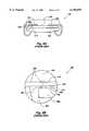
- FIG. 5Ais a cross-sectional side view of a prior art packaged SOJ semiconductor device
- FIG. 5Bis an enlarged cross-sectional side view of a prior art packaged SOJ semiconductor device
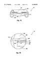
- FIG. 6Ais a cross-sectional side view of a packaged SOJ semiconductor device of the invention.
- FIG. 6Bis an enlarged cross-sectional side view of the packaged SOJ semiconductor device of FIG. 6A;
- FIG. 7Ais a cross-sectional side view of another embodiment of a packaged SOJ semiconductor device of the invention.
- FIG. 7Bis an enlarged cross-sectional side view of the packaged SOJ semiconductor device of FIG. 7A;
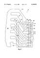
- FIG. 8is a plan view of a die-lead frame assembly of a semiconductor device of the invention.
- FIG. 9is a plan view of another embodiment of a die-lead frame assembly of a semiconductor device of the invention.
- transfer moldingis descriptive of this process as the molding compound (encapsulant), once melted, is transferred under pressure to a plurality of remotely-located mold cavities containing die assemblies to be encapsulated.
- FIG. 1depicts the typical process sequence for plastic package molding. It should be noted that the solder dip/plate operation has been shown as one step for brevity; normally coating would occur prior to the "trim and form” step.
- FIGS. 2A and 2Bshow pre-molding and post-molding positions of encapsulant 30 during a transfer molding operation using a typical mold apparatus 24 comprising upper and lower mold halves 10 and 12, each mold half including a platen 14 or 16 with its associated chase 18 or 20. Heating elements 22 are employed in the platens 14, 16 to maintain an elevated and relatively uniform temperature in the runners 38, 40 and mold cavities 44 during the molding operation.
- FIG. 3is a top view showing one side of the transfer mold apparatus 24 of FIGS. 2A and 2B.
- a die assembly 100is placed in each mold cavity 44 for encapsulation.
- the encapsulant (resin mold compound) 30flows into each mold cavity 44 through the short end.
- each die assembly 100is within a mold cavity 44, and comprises a die 102 with an attached lead frame 104.
- the die assemblies 100are typically disposed in strips so that a strip of e.g. six lead frames 104 (see FIGS. 4A, 4B) may be cut and placed in and across the six cavities 44 shown in FIG. 3.
- Air in the primary runners 38, secondary runners 40 and mold cavities 44is vented to the atmosphere through vents 46 and 48.
- the encapsulant 30is "packed" by application of a higher pressure to eliminate voids and reduce non-uniformities of the encapsulant in the mold cavities 44.
- the encapsulated die assemblies 60are ejected from the cavities 44 by ejector pins 50, after which they are post-cured at an elevated temperature to complete cross-linking of the encapsulating thermoset resin, followed by other operations as known in the art and set forth in FIG. 1 by way of example.
- the flow of encapsulant 30 in the mold cavities 44is demonstrably non-uniform.
- the presence of the die assembly 100comprising a die 102 with lead frame 104 disposed across the mid-section of a cavity 44 splits the viscous encapsulant flow front 54 into upper 56 and lower 58 components.
- the presence of the (relatively) large die 102 with its relatively lower temperature in the middle of a cavity 44permits the flow front 54 on each side of the die 102 to advance ahead of the front which passes over and under the die 102.
- FIG. 4A and 4Bshow two mold cavity encapsulant flow scenarios where, respectively, the lower flow front 58 and the upper flow front 56 lead the overall encapsulant flow front 54 in the cavity 44 containing the die assembly 100.
- FIG. 4Cdepicts the advance of a typical flow front 54 from above, before and after a die 102 is encountered, the flow being depicted as time-separated instantaneous flow fronts 54A, 54B, 54C, 54D, 54E and 54F.
- FIGS. 5A and 5Bdepict a packaged LOC assembly 60 formed by transfer molding, wherein hard filler particles 130 incorporated in the encapsulant become lodged between lead ends 122 and the underlying die surfaces 116 of the die 102.
- the non-uniform flow characteristics of the viscous encapsulant 30, as described above,may cause (in addition to other phenomena such as wire sweep, which this invention does not address) particles 130 to be more forcefully driven into the spaces 126 between the leads 112 and the die 102 and wedged or jammed in place in low-clearance areas.
- the encapsulant flow front 54advances (see FIG. 4C) and the mold operation is completed by packing the cavities or spaces 126, pressure in substantially all portions of the cavities reaches hydrostatic.
- FIG. 5Adepicts a prior art packaged LOC assembly 60 wherein a single lead 112 extends over a die 102, with a segment of dielectric adhesive 114, in this instance a piece of polyimide tape, adhered to both the lead 112 and the active surface 116 of the die.
- a segment of dielectric adhesive 114in this instance a piece of polyimide tape
- filler particle 130which is part of the packaging material 134, is lodged between lead 112 and die surface 116. It is clear that the lead end 122 is tightly constrained from movement by the inflexibility of the attachment of the lead end 122 to the die 102 by adhesive 114.
- the relative closeness of the lead 112 to the active surface 116 and the inability of the lead 112 to flex or relax to reduce stress occasioned by the presence of the filler particle 130may continue even after the encapsulant has reached hydrostatic balance such that the filler particle may become tightly lodged and wedged between the lead 112 and the active surface 116.
- the present invention described belowprovides relief from the particle caused stresses in the die, as well as in the lead 112.
- a packaged LOC semiconductor device 70 of the inventioncomprises at least one lead end 122 of lead 112, the lead end extending over, and spaced from die 102.
- a single bond wire 106 between a bond site 108 on a lead end 122 and a bond pad 110 on the active surface 116 of die 102is shown.
- each of a plurality of lead ends 122is conductively attached to a bond pad 110 by an e.g. thin gold bond wire 106.
- the conductive connections between the die 102 and the lead ends 122may be by tape automated bonding (TAB), whereby the lead ends are bonded directly to bond pads 110 by methods known in the art.
- TABtape automated bonding
- Each of the lead ends 122is shown attached to the die 102 by an intervening layer 114 of dielectric adhesive, which may be e.g. a polyimide film or adhesive tape such as KAPTONTM tape, a trademark of DuPont.
- dielectric adhesivemay be e.g. a polyimide film or adhesive tape such as KAPTONTM tape, a trademark of DuPont.
- the undersurface 128 of the lead end 122is relatively hard when compared to the die surface 116 which is typically a glass.
- particles 130 of filler material in the encapsulantare forced by the flow front of encapsulant into the initial space or recess 126 between the lead end 122 and the die surface 116 along the outer edge 136 of the die 102. Pressure of the hard particles 130 against the die surface 116 occasionally leads to damage of the die 102.
- a displaceable stress relief layer 140also called a displaceable layer herein
- the stress relief layer 140need only extend from the outer edge 138 of the dielectric adhesive 114 to the outer edge 136 of the die 102, it may extend further inward to the inner ends 144 of the leads 112, and be an intervening layer between the lead undersurface 128 and the layer 114 of dielectric adhesive.
- an advantage of such extensionis that when the stress relief layer 140 is formed of elemental silver or similar metal/alloy, the bond between the lead ends 122 and the dielectric adhesive layer 114 is believed to be significantly enhanced, thus avoiding debonding which occasionally occurs in the prior art.
- the stress relief layer 140may also extend outwardly away from the outer edge 136 of the die 102 to ensure full coverage over the space or recess 126. However, such extension is preferably only a short distance, particularly when the layer 140 comprises a costly metal. Thus, at one extreme, the stress relief layer 140 may cover the undersurface 128 of the lead end 122 adjacent the space or recess 126 only. At the other extreme, the stress relief layer 140 may cover the entire undersurface 128 of the lead 112. Depending upon the particular application and the composition of the stress relief layer 140, a preferred embodiment typically includes a soft material layer covering the undersurface 128 adjacent both space or recess 126 and the dielectric adhesive layer 114.
- the stress relief layer 140comprises soft material on the undersurface 128 of the lead end 122.
- the stress relief layer 140absorbs the energy of impinging filler particles 130.
- a particle or particles 130 forcibly entering the space 126 between the die 102 and the lead end 122will preferentially penetrate the soft material layer 140.
- the soft material of the stress relief layer 140has preferentially less than about 1/2 the hardness value of the opposing surface, e.g. die surface 116, contacted by the hard filler particles 130.
- the stress relief layer 140must have a hardness value sufficient to prevent sloughing off of soft material therefrom.
- a hardness of about 0.05 to about 0.5 times that of the die surface 116is preferred.
- the Brinell hardness of the compression layer 140will be less than about 40-50 but at least about 5-10 Brinnel units.
- the particular desired property of the stress relief layer 140is, in actuality, the ease with which it may be penetrated by a hard object. Hardness, as measured by the Brinell or other scale, is a convenient and fairly accurate measure of this property, but other properties which reflect penetrability may be alternatively specified.
- the material of the stress relief layer 140may be a soft metal such as essentially pure silver or other relatively inert metal, or an alloy thereof with a generally low hardness, including pure metals such as palladium and platinum and their alloys.
- the soft materialmust be generally inert under manufacturing, encapsulating and post-encapsulation conditions to avoid detrimental chemical reactions with other chemical species during and following encapsulation. Because of this restriction, together with cost considerations, the number of possible metals which may find practical use as a stress relief layer 140 is limited. However, silver has been found to be an excellent material for the stress relief layer 140 in terms of hardness (about 25-35 Brinell units), chemical resistance, and cost.
- silver platingis typically used as an external protective layer over the e.g. aluminum lead frame following its manufacture and prior to bonding it to the die 102.
- most or all of the silveris removed by e.g. etching prior to die-to-lead frame bonding to enhance bonding and/or for silver recovery.
- silvermay be left on the wire bond sites to enhance electrical connection, a silver oxide layer may form on the silver, resulting in wire bonds of lower strength.
- all of the silver coatingmay be removed prior to die-to-lead frame bonding.
- the very thin layer of silver oxide on the silver platedoes not significantly increase the hardness value for the purposes of this invention.
- the preferred methodincludes removal of all (or nearly all) silver from the lead frame 104 except that which is to form the stress relief layer 140.
- the thickness of the silver stress relief layer 140is generally about one to five microns, which is sufficient to provide the opportunity for relatively deep penetration by filler particles 130. Of course, the preferred thickness is the minimum which will provide the desired protection of the die 102.
- the metal stress relief layer 140may also be attached to the undersurface 128 of the lead end 122 by adhesive.
- the soft material of the stress relief layer 140may be a polymer designed to have a low hardness, at least during the encapsulation process.
- polymersare known and include epoxies, polyimides, acrylics, and silicones.
- the polymeric material hardness prior to encapsulationis less than about one-half the hardness of the die 102 or the coating thereon.
- the polymeric stress relief layer 140may subsequently harden further by, e.g., post-encapsulation thermal treatment, but will have served its purpose in absorbing forces exerted by filler particles 130 during the encapsulant injection step. The preferential penetration of filler particles 130 into the stress relief layer 140 protects the die surface from both immediate and subsequent damage.
- An additional advantage of using a stress relief layer 140 formed of a soft polymeris the additional electrical insulation provided thereby. Use of such a stress relief layer 140 may make possible a decrease in the required thickness of the adhesive layer 114, e.g. dielectric tape.
- FIGS. 7A and 7Bdiffers from that of FIGS. 6A and 6B only in that a coating 148 of adhesive dielectric material is applied to non-wirebonding areas of the surface 116 of die 102 prior to attachment of the dielectric adhesive layer 114 thereto. While this coating 148 provides a degree of protection to the die surface 116, it has been found that the hard filler particles 130 nevertheless may penetrate the coating or high forces transmitted through the coating and damage the die surface.
- a stress relief layer 140is fixed on the undersurface 128 of the leads 112 and absorbs stresses which are otherwise placed upon and through the coating 148 to the die surface 116.
- the stress relief layer 140has a hardness value of less than about 1/2 of the hardness value of the coating 148.
- FIG. 8shows a portion of a LOC semiconductor device 70 as described above in relation to FIGS. 7A and 7B, including die 102 with bond pads 110 and a lead frame 104 with leads 112 extending over peripheral portions of the die. Conductive wires 106 are shown connecting bond pads 110 with bond sites 108 on the lead ends 122.
- the outer edge 136 of the die 102, the outer edge 146 of the coating 148, the outer edge 138 of adhesive layer 114 overlying the coating 148, and the outer edge 124 of the stress relief layer 140 (on the undersurface of the leads 112)are shown as typically configured.
- the portion of the leads 112 having a stress relief layer 140 on the undersurface thereofis shown as hatched, in both FIGS. 8 and 9.
- a stress relief layer 140 of the inventionis useful for any device configuration in which at least one lead overlies, faces, and is spaced from the die surface to create a recess therebetween.
- FIG. 9depicts a different LOC semiconductor device 70 in which the leads 112A overlying the die 102 are in the central portion of the die, while leads 112B not adhered to the die are connected by wires to peripheral bond pads 110B.
- leads 112Acomprise bus bars.
- the outer edge 136 of the die 102, the outer edge 146 of the coating 148, the outer edge 138 of adhesive layer 114 overlying the coating 148, and the outer edge 124 of the stress relief layer 140 (on the undersurface of the leads 112)are shown as typically configured for this type of LOC die-to-lead frame attach.
- a pyramidal indenterwas impinged onto the sample at a peak load of 5 grams.
- the polyimide layerwas penetrated to about 0.7 microns and the silver plate sample was penetrated to about 1.1 microns. Calculation of microhardness by the Vickers method indicated that the hardness of the polyimide surface was about 2.5 times that of the silver plate.
- f.may offer improved adhesion between the lead frame and the die attach material.
Landscapes
- Engineering & Computer Science (AREA)
- Computer Hardware Design (AREA)
- Microelectronics & Electronic Packaging (AREA)
- Power Engineering (AREA)
- Physics & Mathematics (AREA)
- Condensed Matter Physics & Semiconductors (AREA)
- General Physics & Mathematics (AREA)
- Structures Or Materials For Encapsulating Or Coating Semiconductor Devices Or Solid State Devices (AREA)
Abstract
Description
Claims (30)
Priority Applications (3)
| Application Number | Priority Date | Filing Date | Title |
|---|---|---|---|
| US09/298,301US6140695A (en) | 1997-05-15 | 1999-04-23 | Compression layer on the leadframe to reduce stress defects |
| US09/699,918US6486539B1 (en) | 1997-05-15 | 2000-10-30 | Compression layer on the leadframe to reduce stress defects |
| US10/222,103US6657288B2 (en) | 1997-05-15 | 2002-08-16 | Compression layer on the lead frame to reduce stress defects |
Applications Claiming Priority (2)
| Application Number | Priority Date | Filing Date | Title |
|---|---|---|---|
| US08/857,200US5923081A (en) | 1997-05-15 | 1997-05-15 | Compression layer on the leadframe to reduce stress defects |
| US09/298,301US6140695A (en) | 1997-05-15 | 1999-04-23 | Compression layer on the leadframe to reduce stress defects |
Related Parent Applications (1)
| Application Number | Title | Priority Date | Filing Date |
|---|---|---|---|
| US08/857,200ContinuationUS5923081A (en) | 1997-05-15 | 1997-05-15 | Compression layer on the leadframe to reduce stress defects |
Related Child Applications (1)
| Application Number | Title | Priority Date | Filing Date |
|---|---|---|---|
| US09/699,918ContinuationUS6486539B1 (en) | 1997-05-15 | 2000-10-30 | Compression layer on the leadframe to reduce stress defects |
Publications (1)
| Publication Number | Publication Date |
|---|---|
| US6140695Atrue US6140695A (en) | 2000-10-31 |
Family
ID=25325433
Family Applications (5)
| Application Number | Title | Priority Date | Filing Date |
|---|---|---|---|
| US08/857,200Expired - LifetimeUS5923081A (en) | 1997-05-15 | 1997-05-15 | Compression layer on the leadframe to reduce stress defects |
| US09/207,438Expired - LifetimeUS6221695B1 (en) | 1997-05-15 | 1998-12-08 | Method for fabricating a compression layer on the dead frame to reduce stress defects |
| US09/298,301Expired - LifetimeUS6140695A (en) | 1997-05-15 | 1999-04-23 | Compression layer on the leadframe to reduce stress defects |
| US09/699,918Expired - LifetimeUS6486539B1 (en) | 1997-05-15 | 2000-10-30 | Compression layer on the leadframe to reduce stress defects |
| US10/222,103Expired - LifetimeUS6657288B2 (en) | 1997-05-15 | 2002-08-16 | Compression layer on the lead frame to reduce stress defects |
Family Applications Before (2)
| Application Number | Title | Priority Date | Filing Date |
|---|---|---|---|
| US08/857,200Expired - LifetimeUS5923081A (en) | 1997-05-15 | 1997-05-15 | Compression layer on the leadframe to reduce stress defects |
| US09/207,438Expired - LifetimeUS6221695B1 (en) | 1997-05-15 | 1998-12-08 | Method for fabricating a compression layer on the dead frame to reduce stress defects |
Family Applications After (2)
| Application Number | Title | Priority Date | Filing Date |
|---|---|---|---|
| US09/699,918Expired - LifetimeUS6486539B1 (en) | 1997-05-15 | 2000-10-30 | Compression layer on the leadframe to reduce stress defects |
| US10/222,103Expired - LifetimeUS6657288B2 (en) | 1997-05-15 | 2002-08-16 | Compression layer on the lead frame to reduce stress defects |
Country Status (1)
| Country | Link |
|---|---|
| US (5) | US5923081A (en) |
Cited By (12)
| Publication number | Priority date | Publication date | Assignee | Title |
|---|---|---|---|---|
| US6297546B1 (en)* | 1996-05-21 | 2001-10-02 | Micron Technology, Inc. | Underfill coating for LOC package |
| US20030094704A1 (en)* | 2001-01-26 | 2003-05-22 | Gann Keith D. | Method of fabricating known good dies from packaged integrated circuits |
| US6657288B2 (en) | 1997-05-15 | 2003-12-02 | Micron Technology, Inc. | Compression layer on the lead frame to reduce stress defects |
| US20030221313A1 (en)* | 2001-01-26 | 2003-12-04 | Gann Keith D. | Method for making stacked integrated circuits (ICs) using prepackaged parts |
| US6706971B2 (en)* | 2001-01-26 | 2004-03-16 | Irvine Sensors Corporation | Stackable microcircuit layer formed from a plastic encapsulated microcircuit |
| US20040089717A1 (en)* | 2002-11-13 | 2004-05-13 | Sandisk Corporation | Universal non-volatile memory card used with various different standard cards containing a memory controller |
| US20040103234A1 (en)* | 2002-11-21 | 2004-05-27 | Aviad Zer | Combination non-volatile memory and input-output card with direct memory access |
| US20040210715A1 (en)* | 2003-04-17 | 2004-10-21 | Eliyahou Harari | Memory cards including a standard security function |
| US20050055479A1 (en)* | 2002-11-21 | 2005-03-10 | Aviad Zer | Multi-module circuit card with inter-module direct memory access |
| US20050125584A1 (en)* | 2003-12-09 | 2005-06-09 | Yosi Pinto | Efficient connection between modules of removable electronic circuit cards |
| US7107378B1 (en) | 2000-09-01 | 2006-09-12 | Sandisk Corporation | Cooperative interconnection and operation of a non-volatile memory card and an input-output card |
| US7440774B2 (en) | 2002-04-08 | 2008-10-21 | Socket Mobile, Inc. | Wireless enabled memory module |
Families Citing this family (10)
| Publication number | Priority date | Publication date | Assignee | Title |
|---|---|---|---|---|
| US6384333B1 (en) | 1996-05-21 | 2002-05-07 | Micron Technology, Inc. | Underfill coating for LOC package |
| US6005286A (en)* | 1997-10-06 | 1999-12-21 | Micron Technology, Inc. | Increasing the gap between a lead frame and a semiconductor die |
| TW540123B (en)* | 2002-06-14 | 2003-07-01 | Siliconware Precision Industries Co Ltd | Flip-chip semiconductor package with lead frame as chip carrier |
| DE102005051811A1 (en)* | 2005-10-27 | 2007-05-03 | Infineon Technologies Ag | Semiconductor component with semiconductor chip in surface conductive frame technology has chip carrier on chip connection surface with metallic buffer layer and cover layer |
| US20080067646A1 (en)* | 2006-09-18 | 2008-03-20 | Texas Instruments Incorporated | Semiconductor leadframe for uniform mold compound flow |
| JP4338144B2 (en)* | 2006-12-28 | 2009-10-07 | 財団法人山形県産業技術振興機構 | Organic EL light emitting device and method for manufacturing the same |
| TWI456707B (en)* | 2008-01-28 | 2014-10-11 | Renesas Electronics Corp | Semiconductor device and method of manufacturing same |
| US7564123B1 (en)* | 2008-05-19 | 2009-07-21 | Powertech Technology Inc. | Semiconductor package with fastened leads |
| US8058677B2 (en)* | 2008-06-26 | 2011-11-15 | Texas Instruments Incorporated | Stress buffer layer for ferroelectric random access memory |
| US8963343B1 (en)* | 2013-09-27 | 2015-02-24 | Cypress Semiconductor Corporation | Ferroelectric memories with a stress buffer |
Citations (39)
| Publication number | Priority date | Publication date | Assignee | Title |
|---|---|---|---|---|
| US3750277A (en)* | 1970-10-23 | 1973-08-07 | Texas Instruments Inc | Method of making lead frames for semiconductor devices |
| US4209355A (en)* | 1978-07-26 | 1980-06-24 | National Semiconductor Corporation | Manufacture of bumped composite tape for automatic gang bonding of semiconductor devices |
| JPH01207939A (en)* | 1988-02-16 | 1989-08-21 | Seiko Epson Corp | Integrated circuit device assembly tape |
| US4862245A (en)* | 1985-04-18 | 1989-08-29 | International Business Machines Corporation | Package semiconductor chip |
| US4942454A (en)* | 1987-08-05 | 1990-07-17 | Mitsubishi Denki Kabushiki Kaisha | Resin sealed semiconductor device |
| US4984059A (en)* | 1982-10-08 | 1991-01-08 | Fujitsu Limited | Semiconductor device and a method for fabricating the same |
| US5016084A (en)* | 1988-12-08 | 1991-05-14 | Mitsubishi Denki Kabushiki Kaisha | Semiconductor device |
| US5068712A (en)* | 1988-09-20 | 1991-11-26 | Hitachi, Ltd. | Semiconductor device |
| US5126820A (en)* | 1985-02-01 | 1992-06-30 | Advanced Micro Devices, Inc. | Thermal expansion compensated metal lead frame for integrated circuit package |
| US5184208A (en)* | 1987-06-30 | 1993-02-02 | Hitachi, Ltd. | Semiconductor device |
| US5227661A (en)* | 1990-09-24 | 1993-07-13 | Texas Instruments Incorporated | Integrated circuit device having an aminopropyltriethoxysilane coating |
| US5231303A (en)* | 1990-05-08 | 1993-07-27 | Seiko Epson Corporation | Semiconductor device with incorporated stress reducing means |
| US5233220A (en)* | 1989-06-30 | 1993-08-03 | Texas Instruments Incorporated | Balanced capacitance lead frame for integrated circuits and integrated circuit device with separate conductive layer |
| US5250841A (en)* | 1992-04-06 | 1993-10-05 | Motorola, Inc. | Semiconductor device with test-only leads |
| US5252853A (en)* | 1991-09-19 | 1993-10-12 | Mitsubishi Denki Kabushiki Kaisha | Packaged semiconductor device having tab tape and particular power distribution lead structure |
| US5260234A (en)* | 1990-12-20 | 1993-11-09 | Vlsi Technology, Inc. | Method for bonding a lead to a die pad using an electroless plating solution |
| US5266834A (en)* | 1989-03-13 | 1993-11-30 | Hitachi Ltd. | Semiconductor device and an electronic device with the semiconductor devices mounted thereon |
| JPH05326814A (en)* | 1992-05-22 | 1993-12-10 | Dainippon Printing Co Ltd | Lead frame for mounting electronic circuit device |
| DE4313797A1 (en)* | 1992-08-06 | 1994-02-10 | Mitsubishi Electric Corp | Conductor for bonding in semiconductor chip - has perforated end section through conducting layer for connection to contact bumps on semiconductor chip |
| US5286679A (en)* | 1993-03-18 | 1994-02-15 | Micron Technology, Inc. | Method for attaching a semiconductor die to a leadframe using a patterned adhesive layer |
| US5304842A (en)* | 1990-10-24 | 1994-04-19 | Micron Technology, Inc. | Dissimilar adhesive die attach for semiconductor devices |
| US5357139A (en)* | 1990-02-28 | 1994-10-18 | Hitachi, Ltd. | Plastic encapsulated semiconductor device and lead frame |
| US5381037A (en)* | 1993-06-03 | 1995-01-10 | Advanced Micro Devices, Inc. | Lead frame with selected inner leads coupled to an inner frame member for an integrated circuit package assemblies |
| US5384487A (en)* | 1993-05-05 | 1995-01-24 | Lsi Logic Corporation | Off-axis power branches for interior bond pad arrangements |
| US5436410A (en)* | 1992-06-22 | 1995-07-25 | Vlsi Technology, Inc. | Method and structure for suppressing stress-induced defects in integrated circuit conductive lines |
| US5461255A (en)* | 1992-09-18 | 1995-10-24 | Texas Instruments Incorporated | Multi-layered lead frame assembly for integrated circuits |
| US5466888A (en)* | 1991-03-20 | 1995-11-14 | Hitachi, Ltd. | Packaged semiconductor device having stress absorbing film |
| US5474958A (en)* | 1993-05-04 | 1995-12-12 | Motorola, Inc. | Method for making semiconductor device having no die supporting surface |
| US5521432A (en)* | 1991-10-14 | 1996-05-28 | Fujitsu Limited | Semiconductor device having improved leads comprising palladium plated nickel |
| US5531860A (en)* | 1993-09-22 | 1996-07-02 | Qpl Limited | Structure and method for providing a lead frame with enhanced solder wetting leads |
| US5545921A (en)* | 1994-11-04 | 1996-08-13 | International Business Machines, Corporation | Personalized area leadframe coining or half etching for reduced mechanical stress at device edge |
| US5561320A (en)* | 1992-06-04 | 1996-10-01 | Texas Instruments Incorporated | Silver spot/palladium plate lead frame finish |
| US5608260A (en)* | 1994-12-30 | 1997-03-04 | International Business Machines Corporation | Leadframe having contact pads defined by a polymer insulating film |
| US5616953A (en)* | 1994-09-01 | 1997-04-01 | Micron Technology, Inc. | Lead frame surface finish enhancement |
| US5619065A (en)* | 1991-09-11 | 1997-04-08 | Gold Star Electron Co., Ltd. | Semiconductor package and method for assembling the same |
| US5684328A (en)* | 1992-07-29 | 1997-11-04 | Samsung Electronics Co., Ltd. | Semiconductor chip package using improved tape mounting |
| US5760468A (en)* | 1994-09-14 | 1998-06-02 | Micron Technology, Inc. | Adhesion enhanced semiconductor die for mold compound packaging |
| US5789804A (en)* | 1995-04-17 | 1998-08-04 | Yamaichi Electronics Co., Ltd. | Contact agency interposed between IC and IC receptacle |
| US5886399A (en)* | 1995-09-20 | 1999-03-23 | Sony Corporation | Lead frame and integrated circuit package |
Family Cites Families (4)
| Publication number | Priority date | Publication date | Assignee | Title |
|---|---|---|---|---|
| JPH04210150A (en)* | 1990-11-30 | 1992-07-31 | San Le-Tsu Kk | Driving device for reciprocating motion |
| US5259841A (en)* | 1991-02-25 | 1993-11-09 | Gemini Trade Overseas Ltd. | Safety syringe |
| US5733800A (en)* | 1996-05-21 | 1998-03-31 | Micron Technology, Inc. | Underfill coating for LOC package |
| US5923081A (en) | 1997-05-15 | 1999-07-13 | Micron Technology, Inc. | Compression layer on the leadframe to reduce stress defects |
- 1997
- 1997-05-15USUS08/857,200patent/US5923081A/ennot_activeExpired - Lifetime
- 1998
- 1998-12-08USUS09/207,438patent/US6221695B1/ennot_activeExpired - Lifetime
- 1999
- 1999-04-23USUS09/298,301patent/US6140695A/ennot_activeExpired - Lifetime
- 2000
- 2000-10-30USUS09/699,918patent/US6486539B1/ennot_activeExpired - Lifetime
- 2002
- 2002-08-16USUS10/222,103patent/US6657288B2/ennot_activeExpired - Lifetime
Patent Citations (41)
| Publication number | Priority date | Publication date | Assignee | Title |
|---|---|---|---|---|
| US3750277A (en)* | 1970-10-23 | 1973-08-07 | Texas Instruments Inc | Method of making lead frames for semiconductor devices |
| US4209355A (en)* | 1978-07-26 | 1980-06-24 | National Semiconductor Corporation | Manufacture of bumped composite tape for automatic gang bonding of semiconductor devices |
| US4984059A (en)* | 1982-10-08 | 1991-01-08 | Fujitsu Limited | Semiconductor device and a method for fabricating the same |
| US5126820A (en)* | 1985-02-01 | 1992-06-30 | Advanced Micro Devices, Inc. | Thermal expansion compensated metal lead frame for integrated circuit package |
| US4862245A (en)* | 1985-04-18 | 1989-08-29 | International Business Machines Corporation | Package semiconductor chip |
| US5184208A (en)* | 1987-06-30 | 1993-02-02 | Hitachi, Ltd. | Semiconductor device |
| US4942454A (en)* | 1987-08-05 | 1990-07-17 | Mitsubishi Denki Kabushiki Kaisha | Resin sealed semiconductor device |
| JPH01207939A (en)* | 1988-02-16 | 1989-08-21 | Seiko Epson Corp | Integrated circuit device assembly tape |
| US5068712A (en)* | 1988-09-20 | 1991-11-26 | Hitachi, Ltd. | Semiconductor device |
| US5016084A (en)* | 1988-12-08 | 1991-05-14 | Mitsubishi Denki Kabushiki Kaisha | Semiconductor device |
| US5266834A (en)* | 1989-03-13 | 1993-11-30 | Hitachi Ltd. | Semiconductor device and an electronic device with the semiconductor devices mounted thereon |
| US5233220A (en)* | 1989-06-30 | 1993-08-03 | Texas Instruments Incorporated | Balanced capacitance lead frame for integrated circuits and integrated circuit device with separate conductive layer |
| US5357139A (en)* | 1990-02-28 | 1994-10-18 | Hitachi, Ltd. | Plastic encapsulated semiconductor device and lead frame |
| US5231303A (en)* | 1990-05-08 | 1993-07-27 | Seiko Epson Corporation | Semiconductor device with incorporated stress reducing means |
| US5227661A (en)* | 1990-09-24 | 1993-07-13 | Texas Instruments Incorporated | Integrated circuit device having an aminopropyltriethoxysilane coating |
| US5418189A (en)* | 1990-09-24 | 1995-05-23 | Texas Instruments Incorporated | Integrated circuit device and method to prevent cracking during surface mount |
| US5304842A (en)* | 1990-10-24 | 1994-04-19 | Micron Technology, Inc. | Dissimilar adhesive die attach for semiconductor devices |
| US5260234A (en)* | 1990-12-20 | 1993-11-09 | Vlsi Technology, Inc. | Method for bonding a lead to a die pad using an electroless plating solution |
| US5466888A (en)* | 1991-03-20 | 1995-11-14 | Hitachi, Ltd. | Packaged semiconductor device having stress absorbing film |
| US5619065A (en)* | 1991-09-11 | 1997-04-08 | Gold Star Electron Co., Ltd. | Semiconductor package and method for assembling the same |
| US5252853A (en)* | 1991-09-19 | 1993-10-12 | Mitsubishi Denki Kabushiki Kaisha | Packaged semiconductor device having tab tape and particular power distribution lead structure |
| US5521432A (en)* | 1991-10-14 | 1996-05-28 | Fujitsu Limited | Semiconductor device having improved leads comprising palladium plated nickel |
| US5250841A (en)* | 1992-04-06 | 1993-10-05 | Motorola, Inc. | Semiconductor device with test-only leads |
| JPH05326814A (en)* | 1992-05-22 | 1993-12-10 | Dainippon Printing Co Ltd | Lead frame for mounting electronic circuit device |
| US5561320A (en)* | 1992-06-04 | 1996-10-01 | Texas Instruments Incorporated | Silver spot/palladium plate lead frame finish |
| US5436410A (en)* | 1992-06-22 | 1995-07-25 | Vlsi Technology, Inc. | Method and structure for suppressing stress-induced defects in integrated circuit conductive lines |
| US5684328A (en)* | 1992-07-29 | 1997-11-04 | Samsung Electronics Co., Ltd. | Semiconductor chip package using improved tape mounting |
| DE4313797A1 (en)* | 1992-08-06 | 1994-02-10 | Mitsubishi Electric Corp | Conductor for bonding in semiconductor chip - has perforated end section through conducting layer for connection to contact bumps on semiconductor chip |
| US5461255A (en)* | 1992-09-18 | 1995-10-24 | Texas Instruments Incorporated | Multi-layered lead frame assembly for integrated circuits |
| US5286679A (en)* | 1993-03-18 | 1994-02-15 | Micron Technology, Inc. | Method for attaching a semiconductor die to a leadframe using a patterned adhesive layer |
| US5474958A (en)* | 1993-05-04 | 1995-12-12 | Motorola, Inc. | Method for making semiconductor device having no die supporting surface |
| US5384487A (en)* | 1993-05-05 | 1995-01-24 | Lsi Logic Corporation | Off-axis power branches for interior bond pad arrangements |
| US5381037A (en)* | 1993-06-03 | 1995-01-10 | Advanced Micro Devices, Inc. | Lead frame with selected inner leads coupled to an inner frame member for an integrated circuit package assemblies |
| US5531860A (en)* | 1993-09-22 | 1996-07-02 | Qpl Limited | Structure and method for providing a lead frame with enhanced solder wetting leads |
| US5616953A (en)* | 1994-09-01 | 1997-04-01 | Micron Technology, Inc. | Lead frame surface finish enhancement |
| US5760468A (en)* | 1994-09-14 | 1998-06-02 | Micron Technology, Inc. | Adhesion enhanced semiconductor die for mold compound packaging |
| US5545921A (en)* | 1994-11-04 | 1996-08-13 | International Business Machines, Corporation | Personalized area leadframe coining or half etching for reduced mechanical stress at device edge |
| US5576246A (en)* | 1994-11-04 | 1996-11-19 | International Business Machines, Corporation | Personalized area leadframe coining or half etching for reduced mechanical stress at device edge |
| US5608260A (en)* | 1994-12-30 | 1997-03-04 | International Business Machines Corporation | Leadframe having contact pads defined by a polymer insulating film |
| US5789804A (en)* | 1995-04-17 | 1998-08-04 | Yamaichi Electronics Co., Ltd. | Contact agency interposed between IC and IC receptacle |
| US5886399A (en)* | 1995-09-20 | 1999-03-23 | Sony Corporation | Lead frame and integrated circuit package |
Non-Patent Citations (4)
| Title |
|---|
| Caroline A. Kovac et al.; "Plastic Package Fabrication"; Electronic Materials Handbook, vol. 1 Packaging; 1989; pp. 470-482. |
| Caroline A. Kovac et al.; Plastic Package Fabrication ; Electronic Materials Handbook, vol. 1 Packaging; 1989; pp. 470 482.* |
| Loius T. Manzione; "AT&T Plastic Packaging of Microelectronic Devices"; 1990; pp. 156-347. |
| Loius T. Manzione; AT&T Plastic Packaging of Microelectronic Devices ; 1990; pp. 156 347.* |
Cited By (29)
| Publication number | Priority date | Publication date | Assignee | Title |
|---|---|---|---|---|
| US6297546B1 (en)* | 1996-05-21 | 2001-10-02 | Micron Technology, Inc. | Underfill coating for LOC package |
| US6657288B2 (en) | 1997-05-15 | 2003-12-02 | Micron Technology, Inc. | Compression layer on the lead frame to reduce stress defects |
| US7107378B1 (en) | 2000-09-01 | 2006-09-12 | Sandisk Corporation | Cooperative interconnection and operation of a non-volatile memory card and an input-output card |
| US7680974B2 (en) | 2000-09-01 | 2010-03-16 | Sandisk Corporation | Cooperative interconnection and operation of a non-volatile memory card and an input-output card |
| US20060264109A1 (en)* | 2000-09-01 | 2006-11-23 | Brewer Wesley G | Cooperative Interconnection and Operation of a Non-Volatile Memory Card and an Input-Output Card |
| US20030094704A1 (en)* | 2001-01-26 | 2003-05-22 | Gann Keith D. | Method of fabricating known good dies from packaged integrated circuits |
| US20030221313A1 (en)* | 2001-01-26 | 2003-12-04 | Gann Keith D. | Method for making stacked integrated circuits (ICs) using prepackaged parts |
| US6706971B2 (en)* | 2001-01-26 | 2004-03-16 | Irvine Sensors Corporation | Stackable microcircuit layer formed from a plastic encapsulated microcircuit |
| US7174627B2 (en) | 2001-01-26 | 2007-02-13 | Irvine Sensors Corporation | Method of fabricating known good dies from packaged integrated circuits |
| US7440774B2 (en) | 2002-04-08 | 2008-10-21 | Socket Mobile, Inc. | Wireless enabled memory module |
| US8023998B2 (en) | 2002-04-08 | 2011-09-20 | Socket Mobile, Inc. | Wireless enabled memory module |
| US20040089717A1 (en)* | 2002-11-13 | 2004-05-13 | Sandisk Corporation | Universal non-volatile memory card used with various different standard cards containing a memory controller |
| US7114659B2 (en) | 2002-11-13 | 2006-10-03 | Sandisk Corporation | Universal non-volatile memory card used with various different standard cards containing a memory controller |
| US20050198424A1 (en)* | 2002-11-13 | 2005-09-08 | Eliyahou Harari | Universal non-volatile memory card used with various different standard cards containing a memory controller |
| US8752765B2 (en) | 2002-11-13 | 2014-06-17 | Sandisk Technologies Inc. | Universal non-volatile memory card used with various different standard cards containing a memory controller |
| US7367503B2 (en) | 2002-11-13 | 2008-05-06 | Sandisk Corporation | Universal non-volatile memory card used with various different standard cards containing a memory controller |
| US8745299B2 (en) | 2002-11-21 | 2014-06-03 | Sandisk Technologies Inc. | Combination non-volatile memory and input-output card with direct memory access |
| US8037229B2 (en) | 2002-11-21 | 2011-10-11 | Sandisk Technologies Inc. | Combination non-volatile memory and input-output card with direct memory access |
| US20050055479A1 (en)* | 2002-11-21 | 2005-03-10 | Aviad Zer | Multi-module circuit card with inter-module direct memory access |
| US20040103234A1 (en)* | 2002-11-21 | 2004-05-27 | Aviad Zer | Combination non-volatile memory and input-output card with direct memory access |
| US20040210715A1 (en)* | 2003-04-17 | 2004-10-21 | Eliyahou Harari | Memory cards including a standard security function |
| US20080067255A1 (en)* | 2003-04-17 | 2008-03-20 | Eliyahou Harari | Memory Cards Including a Standard Security Function |
| US8019942B2 (en) | 2003-04-17 | 2011-09-13 | SanDisk Technologies, Inc. | Memory cards including a standard security function |
| US7305535B2 (en) | 2003-04-17 | 2007-12-04 | Sandisk Corporation | Memory cards including a standard security function |
| US8539183B2 (en) | 2003-04-17 | 2013-09-17 | Sandisk Technologies Inc. | Memory cards including a standard security function |
| US7467249B2 (en) | 2003-12-09 | 2008-12-16 | Sandisk Corporation | Efficient connection between modules of removable electronic circuit cards |
| US7209995B2 (en) | 2003-12-09 | 2007-04-24 | Sandisk Corporation | Efficient connection between modules of removable electronic circuit cards |
| US20060095627A1 (en)* | 2003-12-09 | 2006-05-04 | Yosi Pinto | Efficient connection between modules of removable electronic circuit cards |
| US20050125584A1 (en)* | 2003-12-09 | 2005-06-09 | Yosi Pinto | Efficient connection between modules of removable electronic circuit cards |
Also Published As
| Publication number | Publication date |
|---|---|
| US5923081A (en) | 1999-07-13 |
| US20030001246A1 (en) | 2003-01-02 |
| US6486539B1 (en) | 2002-11-26 |
| US6221695B1 (en) | 2001-04-24 |
| US6657288B2 (en) | 2003-12-02 |
Similar Documents
| Publication | Publication Date | Title |
|---|---|---|
| US6140695A (en) | Compression layer on the leadframe to reduce stress defects | |
| US6297546B1 (en) | Underfill coating for LOC package | |
| US6005286A (en) | Increasing the gap between a lead frame and a semiconductor die | |
| US20070000599A1 (en) | Assembly method for semiconductor die and lead frame | |
| US6590277B1 (en) | Reduced stress LOC assembly | |
| EP1335428B1 (en) | Resin-moulded semiconductor device and method for manufacturing the same | |
| US6373132B2 (en) | Semiconductor die with attached heat sink and transfer mold | |
| KR19990005508A (en) | Semiconductor chip package with double bent tie bar and small die pad | |
| CN115380376A (en) | Copper wire bonds on gold bumps on semiconductor die bonding pads | |
| US5759875A (en) | Reduced filler particle size encapsulant for reduction in die surface damage in LOC packages and method of use | |
| US6538200B2 (en) | Underfill coating for LOC package | |
| JP2771475B2 (en) | Semiconductor device | |
| JPH08125089A (en) | Lead frame, semiconductor device using the same, and method of manufacturing the same |
Legal Events
| Date | Code | Title | Description |
|---|---|---|---|
| STCF | Information on status: patent grant | Free format text:PATENTED CASE | |
| FEPP | Fee payment procedure | Free format text:PAYOR NUMBER ASSIGNED (ORIGINAL EVENT CODE: ASPN); ENTITY STATUS OF PATENT OWNER: LARGE ENTITY | |
| FPAY | Fee payment | Year of fee payment:4 | |
| CC | Certificate of correction | ||
| FPAY | Fee payment | Year of fee payment:8 | |
| FPAY | Fee payment | Year of fee payment:12 | |
| AS | Assignment | Owner name:U.S. BANK NATIONAL ASSOCIATION, AS COLLATERAL AGENT, CALIFORNIA Free format text:SECURITY INTEREST;ASSIGNOR:MICRON TECHNOLOGY, INC.;REEL/FRAME:038669/0001 Effective date:20160426 Owner name:U.S. BANK NATIONAL ASSOCIATION, AS COLLATERAL AGEN Free format text:SECURITY INTEREST;ASSIGNOR:MICRON TECHNOLOGY, INC.;REEL/FRAME:038669/0001 Effective date:20160426 | |
| AS | Assignment | Owner name:MORGAN STANLEY SENIOR FUNDING, INC., AS COLLATERAL AGENT, MARYLAND Free format text:PATENT SECURITY AGREEMENT;ASSIGNOR:MICRON TECHNOLOGY, INC.;REEL/FRAME:038954/0001 Effective date:20160426 Owner name:MORGAN STANLEY SENIOR FUNDING, INC., AS COLLATERAL Free format text:PATENT SECURITY AGREEMENT;ASSIGNOR:MICRON TECHNOLOGY, INC.;REEL/FRAME:038954/0001 Effective date:20160426 | |
| AS | Assignment | Owner name:U.S. BANK NATIONAL ASSOCIATION, AS COLLATERAL AGENT, CALIFORNIA Free format text:CORRECTIVE ASSIGNMENT TO CORRECT THE REPLACE ERRONEOUSLY FILED PATENT #7358718 WITH THE CORRECT PATENT #7358178 PREVIOUSLY RECORDED ON REEL 038669 FRAME 0001. ASSIGNOR(S) HEREBY CONFIRMS THE SECURITY INTEREST;ASSIGNOR:MICRON TECHNOLOGY, INC.;REEL/FRAME:043079/0001 Effective date:20160426 Owner name:U.S. BANK NATIONAL ASSOCIATION, AS COLLATERAL AGEN Free format text:CORRECTIVE ASSIGNMENT TO CORRECT THE REPLACE ERRONEOUSLY FILED PATENT #7358718 WITH THE CORRECT PATENT #7358178 PREVIOUSLY RECORDED ON REEL 038669 FRAME 0001. ASSIGNOR(S) HEREBY CONFIRMS THE SECURITY INTEREST;ASSIGNOR:MICRON TECHNOLOGY, INC.;REEL/FRAME:043079/0001 Effective date:20160426 | |
| AS | Assignment | Owner name:MICRON TECHNOLOGY, INC., IDAHO Free format text:RELEASE BY SECURED PARTY;ASSIGNOR:U.S. BANK NATIONAL ASSOCIATION, AS COLLATERAL AGENT;REEL/FRAME:047243/0001 Effective date:20180629 | |
| AS | Assignment | Owner name:MICRON TECHNOLOGY, INC., IDAHO Free format text:RELEASE BY SECURED PARTY;ASSIGNOR:MORGAN STANLEY SENIOR FUNDING, INC., AS COLLATERAL AGENT;REEL/FRAME:050937/0001 Effective date:20190731 |