US6139972A - Solder paste containment device - Google Patents
Solder paste containment deviceDownload PDFInfo
- Publication number
- US6139972A US6139972AUS09/179,245US17924598AUS6139972AUS 6139972 AUS6139972 AUS 6139972AUS 17924598 AUS17924598 AUS 17924598AUS 6139972 AUS6139972 AUS 6139972A
- Authority
- US
- United States
- Prior art keywords
- donor substrate
- solder
- paste
- containment
- substrate
- Prior art date
- Legal status (The legal status is an assumption and is not a legal conclusion. Google has not performed a legal analysis and makes no representation as to the accuracy of the status listed.)
- Expired - Fee Related
Links
Images


Classifications
- B—PERFORMING OPERATIONS; TRANSPORTING
- B23—MACHINE TOOLS; METAL-WORKING NOT OTHERWISE PROVIDED FOR
- B23K—SOLDERING OR UNSOLDERING; WELDING; CLADDING OR PLATING BY SOLDERING OR WELDING; CUTTING BY APPLYING HEAT LOCALLY, e.g. FLAME CUTTING; WORKING BY LASER BEAM
- B23K3/00—Tools, devices, or special appurtenances for soldering, e.g. brazing, or unsoldering, not specially adapted for particular methods
- B23K3/06—Solder feeding devices; Solder melting pans
- B23K3/0607—Solder feeding devices
- B23K3/0638—Solder feeding devices for viscous material feeding, e.g. solder paste feeding
- H—ELECTRICITY
- H05—ELECTRIC TECHNIQUES NOT OTHERWISE PROVIDED FOR
- H05K—PRINTED CIRCUITS; CASINGS OR CONSTRUCTIONAL DETAILS OF ELECTRIC APPARATUS; MANUFACTURE OF ASSEMBLAGES OF ELECTRICAL COMPONENTS
- H05K3/00—Apparatus or processes for manufacturing printed circuits
- H05K3/30—Assembling printed circuits with electric components, e.g. with resistor
- H05K3/32—Assembling printed circuits with electric components, e.g. with resistor electrically connecting electric components or wires to printed circuits
- H05K3/34—Assembling printed circuits with electric components, e.g. with resistor electrically connecting electric components or wires to printed circuits by soldering
- H05K3/3457—Solder materials or compositions; Methods of application thereof
- H05K3/3485—Applying solder paste, slurry or powder
- B—PERFORMING OPERATIONS; TRANSPORTING
- B23—MACHINE TOOLS; METAL-WORKING NOT OTHERWISE PROVIDED FOR
- B23K—SOLDERING OR UNSOLDERING; WELDING; CLADDING OR PLATING BY SOLDERING OR WELDING; CUTTING BY APPLYING HEAT LOCALLY, e.g. FLAME CUTTING; WORKING BY LASER BEAM
- B23K2101/00—Articles made by soldering, welding or cutting
- B23K2101/36—Electric or electronic devices
- B23K2101/40—Semiconductor devices
- H—ELECTRICITY
- H05—ELECTRIC TECHNIQUES NOT OTHERWISE PROVIDED FOR
- H05K—PRINTED CIRCUITS; CASINGS OR CONSTRUCTIONAL DETAILS OF ELECTRIC APPARATUS; MANUFACTURE OF ASSEMBLAGES OF ELECTRICAL COMPONENTS
- H05K2203/00—Indexing scheme relating to apparatus or processes for manufacturing printed circuits covered by H05K3/00
- H05K2203/01—Tools for processing; Objects used during processing
- H05K2203/0104—Tools for processing; Objects used during processing for patterning or coating
- H05K2203/0113—Female die used for patterning or transferring, e.g. temporary substrate having recessed pattern
- H—ELECTRICITY
- H05—ELECTRIC TECHNIQUES NOT OTHERWISE PROVIDED FOR
- H05K—PRINTED CIRCUITS; CASINGS OR CONSTRUCTIONAL DETAILS OF ELECTRIC APPARATUS; MANUFACTURE OF ASSEMBLAGES OF ELECTRICAL COMPONENTS
- H05K2203/00—Indexing scheme relating to apparatus or processes for manufacturing printed circuits covered by H05K3/00
- H05K2203/03—Metal processing
- H05K2203/0338—Transferring metal or conductive material other than a circuit pattern, e.g. bump, solder, printed component
- Y—GENERAL TAGGING OF NEW TECHNOLOGICAL DEVELOPMENTS; GENERAL TAGGING OF CROSS-SECTIONAL TECHNOLOGIES SPANNING OVER SEVERAL SECTIONS OF THE IPC; TECHNICAL SUBJECTS COVERED BY FORMER USPC CROSS-REFERENCE ART COLLECTIONS [XRACs] AND DIGESTS
- Y10—TECHNICAL SUBJECTS COVERED BY FORMER USPC
- Y10T—TECHNICAL SUBJECTS COVERED BY FORMER US CLASSIFICATION
- Y10T428/00—Stock material or miscellaneous articles
- Y10T428/31504—Composite [nonstructural laminate]
- Y10T428/31678—Of metal
- Y10T428/31681—Next to polyester, polyamide or polyimide [e.g., alkyd, glue, or nylon, etc.]
- Y—GENERAL TAGGING OF NEW TECHNOLOGICAL DEVELOPMENTS; GENERAL TAGGING OF CROSS-SECTIONAL TECHNOLOGIES SPANNING OVER SEVERAL SECTIONS OF THE IPC; TECHNICAL SUBJECTS COVERED BY FORMER USPC CROSS-REFERENCE ART COLLECTIONS [XRACs] AND DIGESTS
- Y10—TECHNICAL SUBJECTS COVERED BY FORMER USPC
- Y10T—TECHNICAL SUBJECTS COVERED BY FORMER US CLASSIFICATION
- Y10T428/00—Stock material or miscellaneous articles
- Y10T428/31504—Composite [nonstructural laminate]
- Y10T428/31721—Of polyimide
Definitions
- This inventionrelates to integrated circuit packaging, and more particularly to solder bumps as interconnections for integrated circuits and packages. Most particularly, this invention relates to solder bump deposition useful in flip-chip and surface mount technology.
- Solder bumpsprovide electrical and/or mechanical connection between two or more substrates.
- Contained paste depositionis a method of depositing solder bumps in which solder paste occupies a containment region or cavity in a so-called containment structure, and where the solder paste containment assembly remains substantially unmoved through the reflow portion of the solder bump formation process.
- the process solder bump formation via contained paste depositionfurther includes dispensing or depositing solder paste into deposition regions (hereinafter also referred to as cavities) in a donor substrate.
- the donor substrate with the solder paste-filled cavitiesmay be flipped over, and is aligned and in contact with or in close proximity to a receiving substrate with patterns of solderable metallization corresponding to the cavities.
- solder paste containment assemblyincluding the donor substrate, receiving substrate and solder paste is heated in a controlled manner, or reflowed.
- the solder powder in the solder pastemelts and, within each containment region on the donor substrate, coalesces into a single solder ball or bump per cavity. As the molten solder ball or bump coalesces, it pushes against the bottom and sides of the paste containment cavity until it reaches an equilibrium position.
- Hard maskstypically made of silicon, ceramic or metal, are the most promising donor substrates because of their versatility and ability to withstand high reflow temperatures.
- Photoimageable polymer maskscommence to burn around 250° C. and are useful only for deposition of low temperature solders.
- polymer film processing equipmentis not a common fixture in semiconductor fabrication facilities.
- photoimageable polymer masksmust be made thin (no more than about 0.5 mm thick) in order to be properly exposed and developed.
- Hard maskscan damage the surface of the substrate being bumped (the receiving substrate) especially if the receiving substrate is a semiconductor wafer or an integrated circuit (IC). Mechanical damage to the receiving substrate surface can occur any time that the hard mask (donor substrate) makes direct contact with the surface of the receiving substrate.
- a solution to the problem of mechanical damage to the receiving substrateis a paste containment apparatus that does not require direct contact between the donor substrate and the surface of the receiving substrate.
- the donor substratetypically a hard mask with paste containment cavities on its surface, is aligned face-to-face with and positioned in close proximity to the receiving substrate.
- One challenge with this approachis transferring the solder bumps across the gap between the donor substrate and the receiving substrate. Moreover, it is necessary that a sufficient solder volume have been deposited and that alignment between the two substrates be maintained.
- volume of the solder bumpKey factors in determining volume of the solder bump are the volumetric metal loading of the solder paste (limited by the random close packing of spherical solder particles), and the volume of the paste containment region or cavity.
- the volume of a solder bump formed by contained paste depositiontends to be no more than about half of the volume of the paste containment cavity in which the solder bump is formed.
- a solder bumpmust protrude out of the containment cavity so that the bump reaches across or bridges the gap and makes contact with solderable metallization on the receiving substrate. If the solder bump, while molten, does not make contact with solderable metallization on the receiving substrate, it will not transfer but rather remain in the cavity, thereby resulting in a defect on the receiving substrate.
- Deep paste containment cavitiesmay provide adequate solder volume, but may not force the solder bump to protrude out of the cavity.
- Shallow paste containment cavitiesmay force the bump to protrude, but may not provide adequate solder volume.
- Large, shallow cavitiesalso may permit the solder bump to move around in the cavity, possibly out of alignment with the solderable metallization on the receiving substrate, such misalignment resulting in defects on the receiving substrate.
- solder paste containment apparatusthat provides that the reflowed solder bump protrude above the surface plane of the donor substrate so as to enable proximity transfer of the solder bumps from a donor to a receiving substrate.
- solder paste containment apparatusthat provides for deposition of adequate solder paste volume on the donor substrate, and, in turn, adequate solder bump volume resulting therefrom.
- solder paste containment apparatusthat provides for alignment between the donor and receiving substrate such that transfer of the solder bumps from the donor to the receiving substrate is facilitated.
- the inventionprovides an improved solder paste containment apparatus that enables proximity (non-contact) bumping of a receiving substrate by urging molten solder bumps to, during reflow, protrude a substantial distance above the surface plane of the donor substrate. Further provided is a solder paste containment apparatus that provides for deposition of adequate solder paste volume on the donor substrate, and, in turn, adequate solder bump volume resulting therefrom. The invention also provides a contained paste deposition apparatus that maintains alignment between the donor and receiving substrate such that transfer of the solder bumps from the donor to the receiving substrate is facilitated.
- the inventionprovides a fractal-like containment cavity wherein the cavity shape promotes protrusion of the solder bump out of the cavity thereby enabling transfer of the solder bump to a receiving substrate with little or no contact between the donor substrate and the receiving substrate. Moreover, the invention provides for solder bumps of increased volume, producing larger solder bumps at a given bump pitch than otherwise produceable.
- solder paste containment apparatusand in particular, the donor substrate and the configuration of the solder paste deposition regions or paste containment cavities within which the solder bump are formed and from which the solder bumps are transferred.
- FIG. 1schematically represents a cross-section of a contained paste deposition assembly.
- FIG. 2depicts a portion of a donor substrate bearing a solder containment region or cavity according to the invention taught herein.
- FIGS. 3, 3A and 3B inclusiveillustrates a donor substrate as in FIG. 2, bearing a solder containment cavity of a predetermined shape and a cross section of a solder bump formed within said solder containment cavity in accordance with the invention taught herein.
- FIGS. 4, 4A through 4E inclusiveillustrates the preferred and some alternative embodiments of the improved donor substrate according to the invention taught herein.
- FIGS. 5, 5A and 5B inclusiveillustrates an alternate embodiment of the invention taught herein.
- FIG. 1schematically represents a cross-section of a contained paste deposition assembly 9 including a donor substrate 10 and a receiving substrate 14.
- the contained paste deposition bump formation or donor substrate 10has a surface bearing solder bumps 12, such donor substrate 10 surface D is alignably placed in close proximity to a receiving substrate 14, said receiving substrate having a receiving surface R. Said receiving surface R further having wettable regions to receive solder bumps transferred from the donor substrate 10 by virtue of the alignable placement of the donor surface D and receiving surface R of the respective donor 10 and receiving 14 substrates.
- the assembly 9may include spacers interposed between the donor substrate 10 and receiving substrate 14, said spacers may encourage close proximity P while discouraging surface contact that could damage the surface of the receiving substrate.
- FIG. 2depicts a portion of a donor substrate 10 bearing an improved solder containment region, referred to, herein as a cavity or bump formation region, 17 according to the invention taught herein.
- the present inventionprovides for an improved contained paste deposition apparatus, said improvement including the provision of a donor substrate 10 bearing a solder containment cavity 17 wherein the geometric characteristics of the containment region, including the cavity, operate to urge the molten solder bump to protrude from the containment cavity and above the surface of the donor substrate.
- FIGS. 3, 3A and 3B inclusiveillustrates a portion of a donor substrate 10 featuring a solder paste containment region or cavity having a predetermined shape 21.
- a representative cross section along axis AA of FIG. 3Ais depicted in FIG. 3B.
- FIG. 3Billustrates the shape of the containment cavity 21 and a solder bump 22 formed within said cavity in accordance with the invention taught herein.
- the solder paste containment region or cavity 21describes a fractal-like shape with two or more stub walls 20 jutting in from the perimeter of the containment cavity.
- any molten solder bump in a donor substrate 10 according to the present inventionremains substantially centered in the containment cavity ensuring that it remains aligned in the appropriate position for consistent transfer.
- Donor substrate 10 containment region or cavity 17, 21 characteristicsare selected to maximize protrusion of the solder bump above the surface of the donor substrate.
- the area of the cavity(as depicted, viewed from a point of view perpendicular to the surface D) was maximized, an operative constraint being each cavity would be tiled up against its nearest neighbors.
- Tilerefers to assembling a repeated two dimensional geometry composed of a single shape and a single size, adjacently, so that a predetermined area is completely covered. Only triangles, hexagons and squares tile in two dimensions. Hexagons provide the maximum containment cavity area for staggered array tiling, while square cavities provide maximum cavity area for regular array tiling.
- the preferred embodimentis square with three or more stub walls (See FIGS. 4 A and B).
- Each solder bumpmust be substantially centered in its respective containment region or cavity to ensure alignment with the solderable metallization on the receiving substrate.
- centering of the solder bumpis encouraged.
- at least three stub wallsare useful in providing centering for the solder bump.
- a pair of stub wallsmay prove useful.
- three stub wallsis the preferred embodiment.
- the preferred embodimentincludes an outer dimension, that is a dimension or distance across the flat, of the containment region of within the range of about 200-250 ⁇ m, although the general functional range for typical applications may suggest dimensions of from about 25 ⁇ m to 2.5 mm arcoss flats.
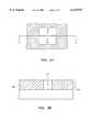
- FIGS. 4, 4A through 4E inclusiveillustrates alternate embodiments of the invention taught herein. More particularly, 4A and 4B illustrate hexagonal solder containment deposition regions or cavities 25 useful in staggered array tiling. 4C and 4D illustrate square solder deposition regions 26 for regular array tiling. 4E illustrates a round solder containment region 27.
- the addition of filleted internal corners and rounded external cornersprovide enhanced mechanical strength and facilitate cleaning of the donor substrate which may be reusable.
- the donor and receiving substratesmay have substantially matching coefficients of thermal expansion and thereby maintain good alignment during reflow. It is also possible to use the same material for both the donor and receiving substrates. Suitable materials for donor substrate include silicon wafer, metal plate, including aluminum, or ceramic, sapphire or glass.
- the containment regionsmay be formed by reactive ion etching, conventional milling or electrical discharge machining.
- the donor substrate 110is a laminate structure of a polymer film, such as, for example, polyimide, over a rigid backer 109, with a solder paste containment region 117 formed in the polymer film by photolithography or laser ablation or some similar manner.
- a polymer filmsuch as, for example, polyimide
Landscapes
- Engineering & Computer Science (AREA)
- Manufacturing & Machinery (AREA)
- Microelectronics & Electronic Packaging (AREA)
- Mechanical Engineering (AREA)
- Electric Connection Of Electric Components To Printed Circuits (AREA)
Abstract
Description
Claims (14)
Priority Applications (3)
| Application Number | Priority Date | Filing Date | Title |
|---|---|---|---|
| US09/179,245US6139972A (en) | 1998-10-26 | 1998-10-26 | Solder paste containment device |
| SG9902918ASG73651A1 (en) | 1998-10-26 | 1999-06-15 | Improved solder paste containment device |
| TW088110091ATW436349B (en) | 1998-10-26 | 1999-06-16 | Solder paste containment device |
Applications Claiming Priority (1)
| Application Number | Priority Date | Filing Date | Title |
|---|---|---|---|
| US09/179,245US6139972A (en) | 1998-10-26 | 1998-10-26 | Solder paste containment device |
Publications (1)
| Publication Number | Publication Date |
|---|---|
| US6139972Atrue US6139972A (en) | 2000-10-31 |
Family
ID=22655800
Family Applications (1)
| Application Number | Title | Priority Date | Filing Date |
|---|---|---|---|
| US09/179,245Expired - Fee RelatedUS6139972A (en) | 1998-10-26 | 1998-10-26 | Solder paste containment device |
Country Status (3)
| Country | Link |
|---|---|
| US (1) | US6139972A (en) |
| SG (1) | SG73651A1 (en) |
| TW (1) | TW436349B (en) |
Cited By (10)
| Publication number | Priority date | Publication date | Assignee | Title |
|---|---|---|---|---|
| US6285081B1 (en)* | 1999-07-13 | 2001-09-04 | Micron Technology, Inc. | Deflectable interconnect |
| US6612027B2 (en) | 1999-09-02 | 2003-09-02 | Micron Technology, Inc. | Method for forming metal contacts on a substrate |
| US6728449B2 (en) | 2002-02-14 | 2004-04-27 | Agilent Technologies, Inc. | Fiber assembly alignment using fiducials |
| US20050161490A1 (en)* | 1999-09-02 | 2005-07-28 | Salman Akram | Method and apparatus for forming metal contacts on a substrate |
| US20110186617A1 (en)* | 2010-02-03 | 2011-08-04 | Hartnett Amanda M | Solder preform |
| US20140053899A1 (en)* | 2012-08-22 | 2014-02-27 | International Business Machines Corporation | Increasing the Efficiency of Solar Cells By Transfer of Solder |
| JP2014151353A (en)* | 2013-02-12 | 2014-08-25 | Calsonic Kansei Corp | Method for manufacturing solder sheet |
| US8993379B2 (en) | 2013-01-21 | 2015-03-31 | International Business Machines Corporation | Chip stack with electrically insulating walls |
| US20170156211A1 (en)* | 2015-11-30 | 2017-06-01 | Cree Fayetteville, Inc. | Method and Device for a High Temperature Vacuum-Safe Solder Stop Utilizing Laser Processing of Solderable Surfaces for an Electronic Module Assembly |
| US10667387B2 (en)* | 2013-04-15 | 2020-05-26 | Ams Sensors Singapore Pte. Ltd. | Accurate positioning and alignment of a component during processes such as reflow soldering |
Families Citing this family (1)
| Publication number | Priority date | Publication date | Assignee | Title |
|---|---|---|---|---|
| US7628871B2 (en) | 2005-08-12 | 2009-12-08 | Intel Corporation | Bulk metallic glass solder material |
Citations (11)
| Publication number | Priority date | Publication date | Assignee | Title |
|---|---|---|---|---|
| US5162257A (en)* | 1991-09-13 | 1992-11-10 | Mcnc | Solder bump fabrication method |
| US5217597A (en)* | 1991-04-01 | 1993-06-08 | Motorola, Inc. | Solder bump transfer method |
| US5307983A (en)* | 1993-04-27 | 1994-05-03 | At&T Bell Laboratories | Method of making an article comprising solder bump bonding |
| US5400950A (en)* | 1994-02-22 | 1995-03-28 | Delco Electronics Corporation | Method for controlling solder bump height for flip chip integrated circuit devices |
| US5447264A (en)* | 1994-07-01 | 1995-09-05 | Mcnc | Recessed via apparatus for testing, burn-in, and/or programming of integrated circuit chips, and for placing solder bumps thereon |
| US5539153A (en)* | 1994-08-08 | 1996-07-23 | Hewlett-Packard Company | Method of bumping substrates by contained paste deposition |
| US5643831A (en)* | 1994-01-20 | 1997-07-01 | Fujitsu Limited | Process for forming solder balls on a plate having apertures using solder paste and transferring the solder balls to semiconductor device |
| US5762259A (en)* | 1995-07-13 | 1998-06-09 | Motorola Inc. | Method for forming bumps on a substrate |
| US5775569A (en)* | 1996-10-31 | 1998-07-07 | Ibm Corporation | Method for building interconnect structures by injection molded solder and structures built |
| US5889326A (en)* | 1996-02-27 | 1999-03-30 | Nec Corporation | Structure for bonding semiconductor device to substrate |
| US6008071A (en)* | 1995-09-20 | 1999-12-28 | Fujitsu Limited | Method of forming solder bumps onto an integrated circuit device |
- 1998
- 1998-10-26USUS09/179,245patent/US6139972A/ennot_activeExpired - Fee Related
- 1999
- 1999-06-15SGSG9902918Apatent/SG73651A1/enunknown
- 1999-06-16TWTW088110091Apatent/TW436349B/ennot_activeIP Right Cessation
Patent Citations (14)
| Publication number | Priority date | Publication date | Assignee | Title |
|---|---|---|---|---|
| US5217597A (en)* | 1991-04-01 | 1993-06-08 | Motorola, Inc. | Solder bump transfer method |
| US5162257A (en)* | 1991-09-13 | 1992-11-10 | Mcnc | Solder bump fabrication method |
| US5307983A (en)* | 1993-04-27 | 1994-05-03 | At&T Bell Laboratories | Method of making an article comprising solder bump bonding |
| US5643831A (en)* | 1994-01-20 | 1997-07-01 | Fujitsu Limited | Process for forming solder balls on a plate having apertures using solder paste and transferring the solder balls to semiconductor device |
| US5400950A (en)* | 1994-02-22 | 1995-03-28 | Delco Electronics Corporation | Method for controlling solder bump height for flip chip integrated circuit devices |
| US5447264A (en)* | 1994-07-01 | 1995-09-05 | Mcnc | Recessed via apparatus for testing, burn-in, and/or programming of integrated circuit chips, and for placing solder bumps thereon |
| US5586715A (en)* | 1994-08-08 | 1996-12-24 | Hewlett-Packard Company | Method of making solder balls by contained paste deposition |
| US5539153A (en)* | 1994-08-08 | 1996-07-23 | Hewlett-Packard Company | Method of bumping substrates by contained paste deposition |
| US5672542A (en)* | 1994-08-08 | 1997-09-30 | Hewlett Packard Company | Method of making solder balls by contained paste deposition |
| US5880017A (en)* | 1994-08-08 | 1999-03-09 | Hewlett-Packard Co. | Method of bumping substrates by contained paste deposition |
| US5762259A (en)* | 1995-07-13 | 1998-06-09 | Motorola Inc. | Method for forming bumps on a substrate |
| US6008071A (en)* | 1995-09-20 | 1999-12-28 | Fujitsu Limited | Method of forming solder bumps onto an integrated circuit device |
| US5889326A (en)* | 1996-02-27 | 1999-03-30 | Nec Corporation | Structure for bonding semiconductor device to substrate |
| US5775569A (en)* | 1996-10-31 | 1998-07-07 | Ibm Corporation | Method for building interconnect structures by injection molded solder and structures built |
Cited By (30)
| Publication number | Priority date | Publication date | Assignee | Title |
|---|---|---|---|---|
| US6664131B2 (en) | 1999-07-13 | 2003-12-16 | Micron Technology, Inc. | Method of making ball grid array package with deflectable interconnect |
| US6501176B2 (en) | 1999-07-13 | 2002-12-31 | Micron Technology, Inc. | Deflectable interconnect |
| US6503777B2 (en) | 1999-07-13 | 2003-01-07 | Micron Technology, Inc. | Deflectable interconnect |
| US20030089985A1 (en)* | 1999-07-13 | 2003-05-15 | Jackson Timothy L. | Deflectable interconnect |
| US20030092218A1 (en)* | 1999-07-13 | 2003-05-15 | Jackson Timothy L. | Deflectable interconnect |
| US6285081B1 (en)* | 1999-07-13 | 2001-09-04 | Micron Technology, Inc. | Deflectable interconnect |
| US6630738B2 (en)* | 1999-07-13 | 2003-10-07 | Micron Technology, Inc | Deflectable interconnect |
| US7131195B2 (en) | 1999-09-02 | 2006-11-07 | Micron Technology, Inc. | Method for forming metal contacts on a substrate |
| US20040031145A1 (en)* | 1999-09-02 | 2004-02-19 | Salman Akram | Method for forming metal contacts on a substrate |
| US20050085063A1 (en)* | 1999-09-02 | 2005-04-21 | Salman Akram | Method for forming metal contacts on a substrate |
| US20050161490A1 (en)* | 1999-09-02 | 2005-07-28 | Salman Akram | Method and apparatus for forming metal contacts on a substrate |
| US20060027632A1 (en)* | 1999-09-02 | 2006-02-09 | Salman Akram | Method for forming metal contacts on a substrate |
| US20060027728A1 (en)* | 1999-09-02 | 2006-02-09 | Salman Akram | Method and apparatus for forming metal contacts on a substrate |
| US6612027B2 (en) | 1999-09-02 | 2003-09-02 | Micron Technology, Inc. | Method for forming metal contacts on a substrate |
| US7156362B2 (en) | 1999-09-02 | 2007-01-02 | Micron Technology, Inc. | Method and apparatus for forming metal contacts on a substrate |
| US7157364B2 (en) | 1999-09-02 | 2007-01-02 | Micron Technology, Inc. | Method for forming metal contacts on a substrate |
| US7156361B1 (en)* | 1999-09-02 | 2007-01-02 | Micron Technology, Inc. | Method and apparatus for forming metal contacts on a substrate |
| US6728449B2 (en) | 2002-02-14 | 2004-04-27 | Agilent Technologies, Inc. | Fiber assembly alignment using fiducials |
| US20110186617A1 (en)* | 2010-02-03 | 2011-08-04 | Hartnett Amanda M | Solder preform |
| US8061578B2 (en)* | 2010-02-03 | 2011-11-22 | Indium Corporation | Solder preform |
| US20140053899A1 (en)* | 2012-08-22 | 2014-02-27 | International Business Machines Corporation | Increasing the Efficiency of Solar Cells By Transfer of Solder |
| US9227259B2 (en)* | 2012-08-22 | 2016-01-05 | International Business Machines Corporation | Increasing the efficiency of solar cells by transfer of solder |
| US8993379B2 (en) | 2013-01-21 | 2015-03-31 | International Business Machines Corporation | Chip stack with electrically insulating walls |
| US9093446B2 (en) | 2013-01-21 | 2015-07-28 | International Business Machines Corporation | Chip stack with electrically insulating walls |
| US9418976B2 (en) | 2013-01-21 | 2016-08-16 | International Business Machines Corporation | Chip stack with electrically insulating walls |
| JP2014151353A (en)* | 2013-02-12 | 2014-08-25 | Calsonic Kansei Corp | Method for manufacturing solder sheet |
| US10667387B2 (en)* | 2013-04-15 | 2020-05-26 | Ams Sensors Singapore Pte. Ltd. | Accurate positioning and alignment of a component during processes such as reflow soldering |
| US20170156211A1 (en)* | 2015-11-30 | 2017-06-01 | Cree Fayetteville, Inc. | Method and Device for a High Temperature Vacuum-Safe Solder Stop Utilizing Laser Processing of Solderable Surfaces for an Electronic Module Assembly |
| US10076800B2 (en)* | 2015-11-30 | 2018-09-18 | Cree Fayetteville, Inc. | Method and device for a high temperature vacuum-safe solder stop utilizing laser processing of solderable surfaces for an electronic module assembly |
| US11135669B2 (en) | 2015-11-30 | 2021-10-05 | Cree, Inc. | Method and device for a high temperature vacuum-safe solder resist utilizing laser ablation of solderable surfaces for an electronic module assembly |
Also Published As
| Publication number | Publication date |
|---|---|
| SG73651A1 (en) | 2001-04-17 |
| TW436349B (en) | 2001-05-28 |
Similar Documents
| Publication | Publication Date | Title |
|---|---|---|
| US5219117A (en) | Method of transferring solder balls onto a semiconductor device | |
| US6139972A (en) | Solder paste containment device | |
| KR100192766B1 (en) | Solder ball planarization method and substrate structure of ball grid array semiconductor package using solder ball as input / output terminals | |
| US5641990A (en) | Laminated solder column | |
| US6020561A (en) | Printed circuit substrate with solder formed on pad-on-via and pad-off-via contacts thereof | |
| US7007833B2 (en) | Forming solder balls on substrates | |
| US7837083B2 (en) | Forming solder balls on substrates | |
| CA1083261A (en) | Method for making conduction-cooled circuit package | |
| US6832747B2 (en) | Hybrid molds for molten solder screening process | |
| US3869787A (en) | Method for precisely aligning circuit devices coarsely positioned on a substrate | |
| US8607446B2 (en) | Method of manufacturing an electronic component | |
| US7560374B2 (en) | Mold for forming conductive bump, method of fabricating the mold, and method of forming bump on wafer using the mold | |
| CN101656216A (en) | Method of manufacturing electronic components having bump | |
| US20140103522A1 (en) | Semiconductor substrate, semiconductor device, and method of manfacturing semiconductor substrate | |
| JPH01109757A (en) | Assembly of integrated circuit chip | |
| US7745321B2 (en) | Solder contacts and methods of forming same | |
| US20070158395A1 (en) | Method for preparing and assembling a soldered substrate | |
| US20070018335A1 (en) | Polygonal, rounded, and circular flip chip ball grid array board | |
| US20050035453A1 (en) | Bump transfer fixture | |
| US20060011712A1 (en) | Improved decal solder transfer method | |
| US6476461B2 (en) | Arrangement of stacked, spherically-shaped semiconductors | |
| WO2013091257A1 (en) | Method for preparing solder lug | |
| JP2002507845A (en) | Method and apparatus for forming solder balls on a substrate | |
| US20050017371A1 (en) | Electronic assembly having a die with rounded corner edge portions and a method of fabricating the same | |
| CN117747582A (en) | Substrate bonding pad for preventing solder ball from shifting |
Legal Events
| Date | Code | Title | Description |
|---|---|---|---|
| AS | Assignment | Owner name:HEWLETT-PACKARD COMPANY, CALIFORNIA Free format text:ASSIGNMENT OF ASSIGNORS INTEREST;ASSIGNORS:TROTT, GARY R.;CHEW, GEARY L.;SHCHWIEBERT, MATTHEW K.;REEL/FRAME:010306/0018;SIGNING DATES FROM 19981029 TO 19981109 | |
| AS | Assignment | Owner name:HEWLETT-PACKARD COMPANY, COLORADO Free format text:MERGER;ASSIGNOR:HEWLETT-PACKARD COMPANY;REEL/FRAME:010759/0049 Effective date:19980520 | |
| AS | Assignment | Owner name:AGILENT TECHNOLOGIES INC, CALIFORNIA Free format text:ASSIGNMENT OF ASSIGNORS INTEREST;ASSIGNOR:HEWLETT-PACKARD COMPANY;REEL/FRAME:010977/0540 Effective date:19991101 | |
| FEPP | Fee payment procedure | Free format text:PAYOR NUMBER ASSIGNED (ORIGINAL EVENT CODE: ASPN); ENTITY STATUS OF PATENT OWNER: LARGE ENTITY | |
| FPAY | Fee payment | Year of fee payment:4 | |
| FPAY | Fee payment | Year of fee payment:8 | |
| REMI | Maintenance fee reminder mailed | ||
| LAPS | Lapse for failure to pay maintenance fees | ||
| STCH | Information on status: patent discontinuation | Free format text:PATENT EXPIRED DUE TO NONPAYMENT OF MAINTENANCE FEES UNDER 37 CFR 1.362 | |
| FP | Lapsed due to failure to pay maintenance fee | Effective date:20121031 |