US6137662A - Magnetoresistive sensor with pinned SAL - Google Patents
Magnetoresistive sensor with pinned SALDownload PDFInfo
- Publication number
- US6137662A US6137662AUS09/055,730US5573098AUS6137662AUS 6137662 AUS6137662 AUS 6137662AUS 5573098 AUS5573098 AUS 5573098AUS 6137662 AUS6137662 AUS 6137662A
- Authority
- US
- United States
- Prior art keywords
- layer
- sal
- antiferromagnetic
- sensing element
- magnetoresistive
- Prior art date
- Legal status (The legal status is an assumption and is not a legal conclusion. Google has not performed a legal analysis and makes no representation as to the accuracy of the status listed.)
- Expired - Lifetime
Links
Images

Classifications
- B—PERFORMING OPERATIONS; TRANSPORTING
- B82—NANOTECHNOLOGY
- B82Y—SPECIFIC USES OR APPLICATIONS OF NANOSTRUCTURES; MEASUREMENT OR ANALYSIS OF NANOSTRUCTURES; MANUFACTURE OR TREATMENT OF NANOSTRUCTURES
- B82Y25/00—Nanomagnetism, e.g. magnetoimpedance, anisotropic magnetoresistance, giant magnetoresistance or tunneling magnetoresistance
- G—PHYSICS
- G01—MEASURING; TESTING
- G01R—MEASURING ELECTRIC VARIABLES; MEASURING MAGNETIC VARIABLES
- G01R33/00—Arrangements or instruments for measuring magnetic variables
- G01R33/02—Measuring direction or magnitude of magnetic fields or magnetic flux
- G01R33/06—Measuring direction or magnitude of magnetic fields or magnetic flux using galvano-magnetic devices
- G01R33/09—Magnetoresistive devices
- G01R33/093—Magnetoresistive devices using multilayer structures, e.g. giant magnetoresistance sensors
- B—PERFORMING OPERATIONS; TRANSPORTING
- B82—NANOTECHNOLOGY
- B82Y—SPECIFIC USES OR APPLICATIONS OF NANOSTRUCTURES; MEASUREMENT OR ANALYSIS OF NANOSTRUCTURES; MANUFACTURE OR TREATMENT OF NANOSTRUCTURES
- B82Y10/00—Nanotechnology for information processing, storage or transmission, e.g. quantum computing or single electron logic
- G—PHYSICS
- G01—MEASURING; TESTING
- G01R—MEASURING ELECTRIC VARIABLES; MEASURING MAGNETIC VARIABLES
- G01R33/00—Arrangements or instruments for measuring magnetic variables
- G01R33/02—Measuring direction or magnitude of magnetic fields or magnetic flux
- G01R33/06—Measuring direction or magnitude of magnetic fields or magnetic flux using galvano-magnetic devices
- G01R33/09—Magnetoresistive devices
- G01R33/096—Magnetoresistive devices anisotropic magnetoresistance sensors
- G—PHYSICS
- G11—INFORMATION STORAGE
- G11B—INFORMATION STORAGE BASED ON RELATIVE MOVEMENT BETWEEN RECORD CARRIER AND TRANSDUCER
- G11B5/00—Recording by magnetisation or demagnetisation of a record carrier; Reproducing by magnetic means; Record carriers therefor
- G11B5/127—Structure or manufacture of heads, e.g. inductive
- G11B5/33—Structure or manufacture of flux-sensitive heads, i.e. for reproduction only; Combination of such heads with means for recording or erasing only
- G11B5/39—Structure or manufacture of flux-sensitive heads, i.e. for reproduction only; Combination of such heads with means for recording or erasing only using magneto-resistive devices or effects
- G11B5/3903—Structure or manufacture of flux-sensitive heads, i.e. for reproduction only; Combination of such heads with means for recording or erasing only using magneto-resistive devices or effects using magnetic thin film layers or their effects, the films being part of integrated structures
- G11B5/3906—Details related to the use of magnetic thin film layers or to their effects
- G11B5/3929—Disposition of magnetic thin films not used for directly coupling magnetic flux from the track to the MR film or for shielding
- G11B5/3932—Magnetic biasing films
- G—PHYSICS
- G11—INFORMATION STORAGE
- G11B—INFORMATION STORAGE BASED ON RELATIVE MOVEMENT BETWEEN RECORD CARRIER AND TRANSDUCER
- G11B5/00—Recording by magnetisation or demagnetisation of a record carrier; Reproducing by magnetic means; Record carriers therefor
- G11B5/127—Structure or manufacture of heads, e.g. inductive
- G11B5/33—Structure or manufacture of flux-sensitive heads, i.e. for reproduction only; Combination of such heads with means for recording or erasing only
- G11B5/39—Structure or manufacture of flux-sensitive heads, i.e. for reproduction only; Combination of such heads with means for recording or erasing only using magneto-resistive devices or effects
- G11B2005/3996—Structure or manufacture of flux-sensitive heads, i.e. for reproduction only; Combination of such heads with means for recording or erasing only using magneto-resistive devices or effects large or giant magnetoresistive effects [GMR], e.g. as generated in spin-valve [SV] devices
Definitions
- This inventionrelates generally to magnetoresistive (MR) read heads, and more particularly to methods and apparatus for providing a SAL bias for a MR sensing element.
- MRmagnetoresistive
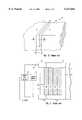
- Magnetic disk drivesare used to store and retrieve data for digital electronic apparatus such as computers.
- a magnetic disk drive D of the prior artincludes a sealed enclosure 1, a disk drive motor 2, a magnetic disk 3, supported for rotation by a spindle S1 of motor 2, an actuator 4 and an arm 5 attached to a spindle S2 of actuator 4.
- a suspension 6is coupled at one end to the arm 5, and at its other end to a read/write head or transducer 7.
- the transducer 7is typically an inductive write element with a sensor read element.
- an air bearingis formed under the transducer 7 to lift it off the surface of the disk 3.
- Various magnetic "tracks" of informationcan be read from the magnetic disk 3 as the actuator 4 is caused to pivot in a short arc as indicate by the arrows P.
- the design and manufacture of magnetic disk drivesis well known to those skilled in the art.
- a magnetoresistive (MR) sensoris used to detect magnetic field signals by means of a changing resistance in a read element.
- a conventional MR sensorutilizes the anisotropic magnetoresistive (AMR) effect for such detection, where the read element resistance varies in proportion to the square of the cosine of the angle between the magnetization in the read element and the direction of a sense current flowing through the read element.
- AMRanisotropic magnetoresistive
- MR sensorsexhibit a number of desirable characteristics. For example, an MR sensor exhibits good linear density resolution and has an output signal strength that is independent of the relative velocity between sensor and medium.
- the longitudinal biasis used to suppress Barkhausen noise which is generated by multi-domain activities within the MR element and to improve the magnetic stability in the presence of high magnetic field excitation.
- the transverse bias fieldis used to bias the MR material so that its response to a magnetic field is in a linear range and of a high differential magnitude.
- the transverse bias fieldis normal to the plane of the magnetic media and parallel to the surface of the planar MR element, and is usually provided by a layer of soft magnetic material deposited proximate to the MR element and magnetized by a magnetic field generated by a current flow in the MR element.
- the soft magnetic materialis often referred to as a "Soft Adjacent Layer” or “SAL” and, as such, this form of biasing is often referred to as "SAL biasing.”
- SAL of the prior artis separated from the MR element by a thin nonmagnetic layer.
- MR sensors using a SAL for transverse biasoften exhibit magnetic instability in the sensor end or tail region and significant side-track reading.
- the height of the MR elementis relatively small, e.g. less than 1 micrometer (um).
- the unsaturated soft magnetic layermay also cause Barkhausen noise in the sensor. What is needed then, is a method for stabilizing the soft magnetic layer and insuring that it is saturated.
- One method for achieving the above-stated goalis the use of the phenomenon of exchange anisotropy. It occurs as a result of the interaction of a ferromagnetic material in contact with an antiferromagnetic material, and can be described in terms of an exchange interaction between magnetic moments on each side of the interface between the two materials.
- exchange coupling between thin layers of ferromagnetic nickel-iron (NiFe) and antiferromagnetic iron-manganese (FeMn)produces a unidirectional anisotropy.
- Improved transverse bias schemes for AMR sensors in which a SAL is stabilized by exchange coupling to an antiferromagnetic (AF) layerwas proposed by Hardayal S. Gill et al. in U.S. Pat. No. 5,508,866.
- GMRgiant magnetoresistance
- a CIP GMR ML sensorprovides a "current-in-plane" (CIP) sensing current as is well known to those skilled in the art.
- a shielded magnetoresistive head (MRH) 10includes a first shield 12, a second shield 14, and a MR sensor 16 disposed within a gap (G) between shields 12 and 14.
- the MR sensormay be centered in the gap G, or may be offset to provide a self-bias, as is well known to those skilled in the art. Lines of magnetic flux impinging upon the MR sensor to create a detectable change in resistance.
- An air bearing surface Sis defined by the MRH 10.
- the MR sensorcan be an AMR sensor or a GMR sensor.
- the design and manufacture of magnetoresistive heads, such as MRH 10is well known to those skilled in the art.
- FIG. 2a cross-sectional view taken along line 2--2 of FIG. 1C illustrates the structure of a MR sensor 16 of the prior art.
- the MR sensor 16includes an MR sensing element 18, a spacer layer 20, a SAL layer 22, and antiferromagnetic (AFM) layer 24.
- the MR element 18can be either an AMR element or a GMR element.
- the SAL layeris typically made from a high resistivity, soft ferromagnetic material such as doped Permalloy. As is well known to those skilled in the art, Permalloy is a magnetic material nominally including 81% nickel (Ni) and 19% iron (Fe).
- the spacer layer 20is typically a nonmagnetic metal such as tantalum for AMR, and copper for GMR.
- the AFM layer 24is used to set the magnetic direction of the SAL 22, as will be discussed in greater detail below.
- the MR sensor 16is supported by a substrate 17 and a buffer layer 19. Ferromagnetic end regions 21 abut the ends of the sensor 16. Leads 25, typically made from gold or other low resistance material, bring the current to the sensor 16. A capping layer 27 is provided over the AFM layer 24. A current source 29 provides a current I b to flow through the various layers of the sensor 16, and signal detection circuitry 31 detects changes in resistance of the sensor 16 as it encounters magnetic fields.
- the MR element 18can have a total magnetization as illustrated by the arrow 26, while the SAL 22 is magnetized as indicated by the arrow 28. Absent the magnetic coupling of the SAL, the MR sensor may have a magnetization as indicated by the dashed arrow 30.
- the actual magnetic angle 26is the sum of the magnetic angle 30 and the magnetostatically coupled magnetic field 28 of the SAL.
- the magnetization 28 of the SAL 22 at a right angle to the magnetization 30 of the MR element 18biases the free element to a point 32 (with a 45° angle) on a R vrs.
- H curve 34that is relatively linear as indicated by the dashed line 36, and which has a relatively large slope m. Linearity is, of course, desirable to provide a linear response, and the relatively large slope is desirable in that it produces large resistance changes in response to the changes in the magnetic field.
- the SAL biasing methodhas a shortcoming in that a relatively high current (e.g. >10 7 amp/cm 2 ) is needed to saturate the SAL to obtain an adequate biasing level. This becomes very pronounced as the height of the AMR element is reduced to 1 micron or less. Additionally, as noted previously, AMR sensors using a SAL transverse bias often exhibit magnetic instability in the sensor or tail region and significant side-track reading. Further, for GMR ML, GMR magnitude was observed to decrease with increasing sense current due to a rise in the temperature of the sensor elements and, therefore, GMR must be optimized for a realistic sense current.
- a relatively high currente.g. >10 7 amp/cm 2
- an improved exchange coupled SAL transverse bias schemeis used to bias AMR and CIP GMR ML sensors. More particularly, for AMR sensors, the SAL is made from a soft magnetic material with a high magnetic moment, and is separated from the magnetoresistive element by a spacer layer.
- a magnetoresistive sensor in accordance with the present inventionincludes a magnetoresistive sensing element, a nonmagnetic layer ("spacer") contacting the magnetoresistive sensing element; an antiferromagnetic (AFM) layer contacting the nonmagnetic layer such that the nonmagnetic layer is sandwiched between the magnetoresistive sensing element and the antiferromagnetic layer; and a ferromagnetic soft adjacent layer (SAL) contacting the antiferromagnetic layer such that the antiferromagnetic layer is sandwiched between the nonmagnetic layer and the soft adjacent layer.
- AFMantiferromagnetic
- SALferromagnetic soft adjacent layer
- the magnetoresistive sensing elementis a magnetoresistive (AMR) sensing element comprising a soft ferromagnetic layer.
- the magnetoresistive sensing elementis giant magnetoresistive (GMR) sensing element comprising a plurality of layers.
- the material of the soft adjacent layeris preferably made from NiFeRh, NiFeNb or a Co-based alloy.
- the material of the antiferromagnetic layeris preferably made from FeMn, RhMn, IrMn, NiO or NiCoO.
- the nonmagnetic layeris preferably made from Ti or Ta.
- the bias schemecan be non-symmetric, or may be symmetric around the magnetoresistive sensing element.
- a second antiferromagnetic layercan be provided to be a second pinning layer for the "pinned" SAL layer.
- the exchange biased bilayercan further have a multilayered structure such as AFM/SAL/AFM/SAL. . . .
- the SAL layercan be thin, so that a high exchange field with a high resistance can be obtained.
- An advantage of this structureis that the provision of pinning layers on both sides of the pinned layer results in the strengthening of the pinning of the pinned layer. Furthermore, the symmetric and multiple-layer configurations provide a more uniform bias field and a large bias magnitude at the price of some additional fabrication complexity.
- FIG. 1Ais a partially sectioned, front elevational view of a magnetic disk drive assembly
- FIG. 1Bis a cross section taken along line 1B--1B of FIG. 1A;
- FIG. 1Cis a perspective view of a prior art shielded vertical magnetoresistive (MR) read head
- FIG. 2is a cross-sectional view of the magnetoresistive (MR) sensor taken along line 2--2 of FIG. 1C;
- FIG. 3illustrates the magnetization of the magnetoresistive MR sensing element and of the soft adjacent layer (SAL) of the MR sensor of FIG. 2;
- FIG. 4is a graph illustrating the resistance versus magnetic field relationship of the MR sensor
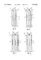
- FIG. 5is a cross section view of an improved MR sensor of the present invention having an exchange biased bilayer of an AFM layer and a SAL layer in a non-symmetrical arrangement with the MR sensing element and a second AFM layer abutting the exchange biased bilayer;
- FIG. 6is a cross sectional view of an improved MR sensor of the present invention with a symmetrical arrangement of the exchange biased bilayers and without the second AFM layer;
- FIG. 7is a cross sectional view of an improved MR sensor of the present invention similar to that of FIG. 5, but with a symmetrical arrangement of the exchange biased bilayers and the AFM layers;
- FIG. 8is a cross sectional view of an improved MR sensor of the present invention having a symmetrical arrangement of AFM and SAL layers.
- a magnetoresistive (MR) sensor 56includes a magnetoresistive (MR) sensing element 42, a nonmagnetic layer (“spacer") 44, an antiferromagnetic (AFM) or “pinning” layer 46, a soft adjacent layer (SAL) or “pinned” layer 48, and a second AFM layer 58.
- This second AFM layer 58provides an additional "pinning" layer for the "pinned” SAL layer 48, which results in a stronger pinning of the SAL layer.
- This MR sensor 56(and the other MR sensors of the present invention described subsequently) preferably form a part of the larger structure and system as illustrated in FIG. 2, where the MR sensors (such as MR sensor 56) of the present invention take the place of the MR sensor 16 of the prior art.
- the nominal direction of the magnetic field in the MR sensing element 42is indicated by arrow 50, while the pinned direction of the magnetic field in the SAL layer is indicated by arrow 52.
- the fringing field from the pinned SALis indicated by arrow 54.
- a magnetoresistive sensor in accordance with the present inventionincludes a magnetoresistive sensing element 42, a nonmagnetic layer 44 contacting the magnetoresistive sensing element 42; an antiferromagnetic layer 46 contacting the nonmagnetic layer 44 such that the nonmagnetic layer 44 is sandwiched between the magnetoresistive sensing element 42 and the antiferromagnetic layer 46; a ferromagnetic soft adjacent layer 48 contacting the antiferromagnetic layer 46 such that the antiferromagnetic layer 46 is sandwiched between the nonmagnetic layer 44 and the soft adjacent layer 48, and a second antiferromagnetic layer 58 contacting the soft adjacent layer 48 such that the soft adjacent layer 48 is sandwiched between the first antiferromagnetic layer 46 and the second antiferromagnetic layer 58.
- the magnetoresistive sensing element 42is a magnetoresistive (AMR) sensing element comprising a soft ferromagnetic layer.
- the magnetoresistive sensing elementis giant magnetoresistive (GMR) sensing element comprising a plurality of layers.
- AMR sensing elements and GMR sensing elementsare well known to those skilled in the art.
- nonmagnetic, SAL, and AFM layersare well known to those skilled in the art.
- an AFM/SAL exchange biased bilayeris the combination of the AFM layer 46 and the SAL layer 48.
- the dual pinning layer structure of the present inventionprovides an enhanced pinning of the pinned layer compared to providing only a single pinning layer. Enhancing the pinning of the pinned layer, in turn, enhances the performance of the sensor.
- an optional additional SAL layer 59Shown in broken lines in FIG. 5 is an optional additional SAL layer 59.
- This additional SAL layerforms a second exchange biased bilayer 53A from the AFM layer 58 and the SAL layer 59. Therefore, a multilayered structure AFM/SAL/AFM/SAL is formed from layers 46/48/58/59, respectively. Further exchange biased bilayers AFM/SAL can also be added, as in AFM/SAL/AFM/SAL AFM/SAL. . . .
- the SAL layercan be made thin, e.g. 20-80 Angstroms, resulting in a high exchange field "H ex " and high resistance "R" SAL layer, thereby reducing the shunting in the sensor.
- FIG. 6Another MR sensor 60 of the present invention is shown in FIG. 6.
- This designis a symmetrical version of the MR sensor 56 of FIG. 5 with the omission of the second antiferromagnetic layer 58, where symmetrical elements are indicated by a prime on the element numbers.
- this symmetrical designproduces both the fringing field 54 from the SAL 48 and a fringing field 54' from the SAL 48'.
- the dual fringing fieldsprovide a more uniform bias field and a large bias magnitude.
- FIG. 7A still further MR sensor 62 of the present invention is shown in FIG. 7.
- This designis a symmetrical version of the MR sensor 56 of FIG. 5 including the second AFM layer 58, where symmetrical elements are indicated by a prime on the element numbers.
- this symmetrical designproduces both the fringing field 54 from the SAL 48 and a fringing field 54' from the SAL 48'.
- the dual fringing fieldsprovide a more uniform bias field and a large bias magnitude, as before.
- the additional AFM layers 58 and 58'provide additional pinning for the SAL layers 48 and 48', as discussed previously.
- An alternate embodiment for an MR sensor 64 of the present inventionis illustrated in FIG. 8.
- the MR sensor 64is of symmetrical design (as were the MR sensors 60 of FIG. 6 and 62 of FIG. 7) but, in this instance, the position of the SAL layers and the AFM layers have been reversed. Therefore, the SAL and AFM layers do not form an exchange biased bilayer, as defined previously.
- the MR sensor 64includes an MR sensing element 66, a nonmagnetic or "spacer” layer 68, a soft adjacent layer or “SAL” 70, and an antiferromagnetic or “AFM” layer 72. Since this is a symmetrical structure, the MR sensor further includes a symmetrically located (with respect to the MR sensing element 66) spacer layer 68', SAL layer 70', and AFM layer 72'.
- the AFM layer 72is the pinning layer for the "pinned" SAL layer 70, while the AFM layer 72' is the pinning layer for the "pinned" SAL layer 70'.
- the magnetic field of the MR sensor 64is shown by arrow 74, while the magnetic fields of the SAL layers 70 and 70' are shown by arrows 76 and 76', respectively.
- the fringing field from the pinned SAL layer 70is shown by arrow 78, and the fringing field from the pinned SAL layer 70' is shown by the arrow 78'.
- the SAL layerwill be in full saturation, and will not become unsaturated under normal operating conditions due to the very strong pinning effect described previously.
- the soft adjacent layers (SALs) or “biasing” layersare made from a soft magnetic material with high magnetic moments. These materials include NiFeRh, NiFeNb or Co-based alloys.
- the biasing layersare exchange coupled with high resistivity or dielectric antiferromagnetic (AFM) layers such as FeMn, RhMn, IrMn, NiO or NiCoO.
- AFMdielectric antiferromagnetic
- the nonmagnetic layers separating the AMR or GMR multilayer elements from the AFM layersare made from a nonmagnetic layer such as Ti or Ta.
- thickness of the nonmagnetic spacer layersis preferably in the range of 10 to 80 Angstroms.
- the thickness of the AFM layersis preferably in the range of 60 to 120 Angstroms.
- the thickness the SAL layersis preferably in the range of 30 to 100 Angstroms.
- the thickness of the MR elementsare dependent upon the technology used for the sensing element.
- the AFM pinning films, the pinned SAL layers, and the nonmagnetic spacer materialsshould be insulating or be made from a material that has a higher resistivity (e.g. at least three times the resistivity) than the resistivity of the AMR or GMR ML sensing elements.
- the SALshould also have a very low magnetoresistive effect.
- the low biasing efficiency of a larger spacer (e.g. 280 Angstroms) between the AMR or GMR ML sensor and the SALcan be compensated by using a thinner SAL (e.g. less than 30 Angstroms) with high magnetic moment, such as the Co-based alloys.
- the oriented magnetic fieldcan be applied to the transverse direction to achieve transverse pinning effect for SAL and the oriented field can be rotated later to 90 degrees when depositing AMR or GMR ML elements to induce the unidirectional anistotropy along the longitudinal direction (i.e. the current flow direction).
Landscapes
- Engineering & Computer Science (AREA)
- Physics & Mathematics (AREA)
- Chemical & Material Sciences (AREA)
- Nanotechnology (AREA)
- Condensed Matter Physics & Semiconductors (AREA)
- General Physics & Mathematics (AREA)
- Crystallography & Structural Chemistry (AREA)
- Manufacturing & Machinery (AREA)
- Mathematical Physics (AREA)
- Theoretical Computer Science (AREA)
- Magnetic Heads (AREA)
- Measuring Magnetic Variables (AREA)
Abstract
Description
Claims (3)
Priority Applications (2)
| Application Number | Priority Date | Filing Date | Title |
|---|---|---|---|
| US09/055,730US6137662A (en) | 1998-04-07 | 1998-04-07 | Magnetoresistive sensor with pinned SAL |
| JP11100147AJPH11316918A (en) | 1998-04-07 | 1999-04-07 | Magnetoresistive sensor, magnetic disk system and reading out/writing head assembly |
Applications Claiming Priority (1)
| Application Number | Priority Date | Filing Date | Title |
|---|---|---|---|
| US09/055,730US6137662A (en) | 1998-04-07 | 1998-04-07 | Magnetoresistive sensor with pinned SAL |
Publications (1)
| Publication Number | Publication Date |
|---|---|
| US6137662Atrue US6137662A (en) | 2000-10-24 |
Family
ID=21999779
Family Applications (1)
| Application Number | Title | Priority Date | Filing Date |
|---|---|---|---|
| US09/055,730Expired - LifetimeUS6137662A (en) | 1998-04-07 | 1998-04-07 | Magnetoresistive sensor with pinned SAL |
Country Status (2)
| Country | Link |
|---|---|
| US (1) | US6137662A (en) |
| JP (1) | JPH11316918A (en) |
Cited By (152)
| Publication number | Priority date | Publication date | Assignee | Title |
|---|---|---|---|---|
| US6396660B1 (en)* | 1999-08-23 | 2002-05-28 | Read-Rite Corporation | Magnetic write element having a thermally dissipative structure |
| US6501271B1 (en)* | 1998-05-11 | 2002-12-31 | Koninkiljke Philips Electronics N.V. | Robust giant magnetoresistive effect type multilayer sensor |
| US20030042903A1 (en)* | 2001-08-29 | 2003-03-06 | Alps Electric Co., Ltd. | Magnetic detection device adapted to control magnetization of free magnetic layer by using antiferromagnetic layer, and manufacturing method for the same |
| US6563681B1 (en)* | 1999-05-31 | 2003-05-13 | Tdk Corporation | Magnetoresistance effect film and magnetoresistance effect type head |
| US6603642B1 (en)* | 2000-03-15 | 2003-08-05 | Tdk Corporation | Magnetic transducer having a plurality of magnetic layers stacked alternately with a plurality of nonmagnetic layers and a fixed-orientation-of-magnetization layer and thin film magnetic head including the magnetic transducer |
| WO2002073226A3 (en)* | 2001-03-14 | 2003-10-16 | Ibm | Tunnel junction and charge perpendicular-to-plane magnetic recording sensors and method of manufacture |
| US20050052788A1 (en)* | 2000-09-11 | 2005-03-10 | Kabushiki Kaisha Toshiba | Magnetoresistance effect element, magnetic head and magnetic recording and/or reproducing system |
| US20060018057A1 (en)* | 2004-07-26 | 2006-01-26 | Yiming Huai | Magnetic tunnel junction having diffusion stop layer |
| US7035062B1 (en)* | 2001-11-29 | 2006-04-25 | Seagate Technology Llc | Structure to achieve sensitivity and linear density in tunneling GMR heads using orthogonal magnetic alignments |
| US7224601B2 (en) | 2005-08-25 | 2007-05-29 | Grandis Inc. | Oscillating-field assisted spin torque switching of a magnetic tunnel junction memory element |
| US20070171694A1 (en)* | 2005-12-23 | 2007-07-26 | Yiming Huai | Current-switched spin-transfer magnetic devices with reduced spin-transfer switching current density |
| US20070246787A1 (en)* | 2006-03-29 | 2007-10-25 | Lien-Chang Wang | On-plug magnetic tunnel junction devices based on spin torque transfer switching |
| US20080061388A1 (en)* | 2006-09-13 | 2008-03-13 | Zhitao Diao | Devices and circuits based on magnetic tunnel junctions utilizing a multilayer barrier |
| US20080239591A1 (en)* | 2007-03-30 | 2008-10-02 | Kabushiki Kaisha Toshiba | Magneto-resistance effect element, and method for manufacturing the same |
| US20090050991A1 (en)* | 2007-08-22 | 2009-02-26 | Hide Nagai | Magnetic Element Having Low Saturation Magnetization |
| US20090190264A1 (en)* | 2008-01-30 | 2009-07-30 | Kabushiki Kaisha Toshiba | Magnetoresistive element and method of manufacturing the same |
| US20100072524A1 (en)* | 2005-09-20 | 2010-03-25 | Yiming Huai | Magnetic Devices Having Oxide Antiferromagnetic Layer Next To Free Ferromagnetic Layer |
| US7777261B2 (en) | 2005-09-20 | 2010-08-17 | Grandis Inc. | Magnetic device having stabilized free ferromagnetic layer |
| US7894248B2 (en) | 2008-09-12 | 2011-02-22 | Grandis Inc. | Programmable and redundant circuitry based on magnetic tunnel junction (MTJ) |
| US7957179B2 (en) | 2007-06-27 | 2011-06-07 | Grandis Inc. | Magnetic shielding in magnetic multilayer structures |
| US7973349B2 (en) | 2005-09-20 | 2011-07-05 | Grandis Inc. | Magnetic device having multilayered free ferromagnetic layer |
| US8184408B2 (en) | 2008-01-30 | 2012-05-22 | Kabushiki Kaisha Toshiba | Magnetoresistive element and method of manufacturing the same |
| US8830628B1 (en) | 2009-02-23 | 2014-09-09 | Western Digital (Fremont), Llc | Method and system for providing a perpendicular magnetic recording head |
| US8879207B1 (en) | 2011-12-20 | 2014-11-04 | Western Digital (Fremont), Llc | Method for providing a side shield for a magnetic recording transducer using an air bridge |
| US8883017B1 (en) | 2013-03-12 | 2014-11-11 | Western Digital (Fremont), Llc | Method and system for providing a read transducer having seamless interfaces |
| US8917581B1 (en) | 2013-12-18 | 2014-12-23 | Western Digital Technologies, Inc. | Self-anneal process for a near field transducer and chimney in a hard disk drive assembly |
| US8923102B1 (en) | 2013-07-16 | 2014-12-30 | Western Digital (Fremont), Llc | Optical grating coupling for interferometric waveguides in heat assisted magnetic recording heads |
| US8947985B1 (en) | 2013-07-16 | 2015-02-03 | Western Digital (Fremont), Llc | Heat assisted magnetic recording transducers having a recessed pole |
| US8953422B1 (en) | 2014-06-10 | 2015-02-10 | Western Digital (Fremont), Llc | Near field transducer using dielectric waveguide core with fine ridge feature |
| US8958272B1 (en) | 2014-06-10 | 2015-02-17 | Western Digital (Fremont), Llc | Interfering near field transducer for energy assisted magnetic recording |
| US8970988B1 (en) | 2013-12-31 | 2015-03-03 | Western Digital (Fremont), Llc | Electric gaps and method for making electric gaps for multiple sensor arrays |
| US8971160B1 (en) | 2013-12-19 | 2015-03-03 | Western Digital (Fremont), Llc | Near field transducer with high refractive index pin for heat assisted magnetic recording |
| US8976635B1 (en) | 2014-06-10 | 2015-03-10 | Western Digital (Fremont), Llc | Near field transducer driven by a transverse electric waveguide for energy assisted magnetic recording |
| US8982508B1 (en) | 2011-10-31 | 2015-03-17 | Western Digital (Fremont), Llc | Method for providing a side shield for a magnetic recording transducer |
| US8980109B1 (en) | 2012-12-11 | 2015-03-17 | Western Digital (Fremont), Llc | Method for providing a magnetic recording transducer using a combined main pole and side shield CMP for a wraparound shield scheme |
| US8988812B1 (en) | 2013-11-27 | 2015-03-24 | Western Digital (Fremont), Llc | Multi-sensor array configuration for a two-dimensional magnetic recording (TDMR) operation |
| US8988825B1 (en) | 2014-02-28 | 2015-03-24 | Western Digital (Fremont, LLC | Method for fabricating a magnetic writer having half-side shields |
| US8984740B1 (en) | 2012-11-30 | 2015-03-24 | Western Digital (Fremont), Llc | Process for providing a magnetic recording transducer having a smooth magnetic seed layer |
| US8993217B1 (en) | 2013-04-04 | 2015-03-31 | Western Digital (Fremont), Llc | Double exposure technique for high resolution disk imaging |
| US8995087B1 (en) | 2006-11-29 | 2015-03-31 | Western Digital (Fremont), Llc | Perpendicular magnetic recording write head having a wrap around shield |
| US9001467B1 (en) | 2014-03-05 | 2015-04-07 | Western Digital (Fremont), Llc | Method for fabricating side shields in a magnetic writer |
| US9001628B1 (en) | 2013-12-16 | 2015-04-07 | Western Digital (Fremont), Llc | Assistant waveguides for evaluating main waveguide coupling efficiency and diode laser alignment tolerances for hard disk |
| US8997832B1 (en) | 2010-11-23 | 2015-04-07 | Western Digital (Fremont), Llc | Method of fabricating micrometer scale components |
| US9007725B1 (en) | 2014-10-07 | 2015-04-14 | Western Digital (Fremont), Llc | Sensor with positive coupling between dual ferromagnetic free layer laminates |
| US9007879B1 (en) | 2014-06-10 | 2015-04-14 | Western Digital (Fremont), Llc | Interfering near field transducer having a wide metal bar feature for energy assisted magnetic recording |
| US9007719B1 (en) | 2013-10-23 | 2015-04-14 | Western Digital (Fremont), Llc | Systems and methods for using double mask techniques to achieve very small features |
| US9013836B1 (en) | 2013-04-02 | 2015-04-21 | Western Digital (Fremont), Llc | Method and system for providing an antiferromagnetically coupled return pole |
| US9042052B1 (en) | 2014-06-23 | 2015-05-26 | Western Digital (Fremont), Llc | Magnetic writer having a partially shunted coil |
| US9042208B1 (en) | 2013-03-11 | 2015-05-26 | Western Digital Technologies, Inc. | Disk drive measuring fly height by applying a bias voltage to an electrically insulated write component of a head |
| US9042057B1 (en) | 2013-01-09 | 2015-05-26 | Western Digital (Fremont), Llc | Methods for providing magnetic storage elements with high magneto-resistance using Heusler alloys |
| US9042051B2 (en) | 2013-08-15 | 2015-05-26 | Western Digital (Fremont), Llc | Gradient write gap for perpendicular magnetic recording writer |
| US9042058B1 (en) | 2013-10-17 | 2015-05-26 | Western Digital Technologies, Inc. | Shield designed for middle shields in a multiple sensor array |
| US9053735B1 (en) | 2014-06-20 | 2015-06-09 | Western Digital (Fremont), Llc | Method for fabricating a magnetic writer using a full-film metal planarization |
| US9064507B1 (en) | 2009-07-31 | 2015-06-23 | Western Digital (Fremont), Llc | Magnetic etch-stop layer for magnetoresistive read heads |
| US9064527B1 (en) | 2013-04-12 | 2015-06-23 | Western Digital (Fremont), Llc | High order tapered waveguide for use in a heat assisted magnetic recording head |
| US9065043B1 (en) | 2012-06-29 | 2015-06-23 | Western Digital (Fremont), Llc | Tunnel magnetoresistance read head with narrow shield-to-shield spacing |
| US9064528B1 (en) | 2013-05-17 | 2015-06-23 | Western Digital Technologies, Inc. | Interferometric waveguide usable in shingled heat assisted magnetic recording in the absence of a near-field transducer |
| US9070381B1 (en) | 2013-04-12 | 2015-06-30 | Western Digital (Fremont), Llc | Magnetic recording read transducer having a laminated free layer |
| US9082423B1 (en) | 2013-12-18 | 2015-07-14 | Western Digital (Fremont), Llc | Magnetic recording write transducer having an improved trailing surface profile |
| US9087527B1 (en) | 2014-10-28 | 2015-07-21 | Western Digital (Fremont), Llc | Apparatus and method for middle shield connection in magnetic recording transducers |
| US9087534B1 (en) | 2011-12-20 | 2015-07-21 | Western Digital (Fremont), Llc | Method and system for providing a read transducer having soft and hard magnetic bias structures |
| US9093639B2 (en) | 2012-02-21 | 2015-07-28 | Western Digital (Fremont), Llc | Methods for manufacturing a magnetoresistive structure utilizing heating and cooling |
| US9104107B1 (en) | 2013-04-03 | 2015-08-11 | Western Digital (Fremont), Llc | DUV photoresist process |
| US9111558B1 (en) | 2014-03-14 | 2015-08-18 | Western Digital (Fremont), Llc | System and method of diffractive focusing of light in a waveguide |
| US9111564B1 (en) | 2013-04-02 | 2015-08-18 | Western Digital (Fremont), Llc | Magnetic recording writer having a main pole with multiple flare angles |
| US9111550B1 (en) | 2014-12-04 | 2015-08-18 | Western Digital (Fremont), Llc | Write transducer having a magnetic buffer layer spaced between a side shield and a write pole by non-magnetic layers |
| US9123359B1 (en) | 2010-12-22 | 2015-09-01 | Western Digital (Fremont), Llc | Magnetic recording transducer with sputtered antiferromagnetic coupling trilayer between plated ferromagnetic shields and method of fabrication |
| US9123362B1 (en) | 2011-03-22 | 2015-09-01 | Western Digital (Fremont), Llc | Methods for assembling an electrically assisted magnetic recording (EAMR) head |
| US9123358B1 (en) | 2012-06-11 | 2015-09-01 | Western Digital (Fremont), Llc | Conformal high moment side shield seed layer for perpendicular magnetic recording writer |
| US9123374B1 (en) | 2015-02-12 | 2015-09-01 | Western Digital (Fremont), Llc | Heat assisted magnetic recording writer having an integrated polarization rotation plate |
| US9135937B1 (en) | 2014-05-09 | 2015-09-15 | Western Digital (Fremont), Llc | Current modulation on laser diode for energy assisted magnetic recording transducer |
| US9135930B1 (en) | 2014-03-06 | 2015-09-15 | Western Digital (Fremont), Llc | Method for fabricating a magnetic write pole using vacuum deposition |
| US9142233B1 (en) | 2014-02-28 | 2015-09-22 | Western Digital (Fremont), Llc | Heat assisted magnetic recording writer having a recessed pole |
| US9147408B1 (en) | 2013-12-19 | 2015-09-29 | Western Digital (Fremont), Llc | Heated AFM layer deposition and cooling process for TMR magnetic recording sensor with high pinning field |
| US9147404B1 (en) | 2015-03-31 | 2015-09-29 | Western Digital (Fremont), Llc | Method and system for providing a read transducer having a dual free layer |
| US9153255B1 (en) | 2014-03-05 | 2015-10-06 | Western Digital (Fremont), Llc | Method for fabricating a magnetic writer having an asymmetric gap and shields |
| US9183854B2 (en) | 2014-02-24 | 2015-11-10 | Western Digital (Fremont), Llc | Method to make interferometric taper waveguide for HAMR light delivery |
| US9190085B1 (en) | 2014-03-12 | 2015-11-17 | Western Digital (Fremont), Llc | Waveguide with reflective grating for localized energy intensity |
| US9190079B1 (en) | 2014-09-22 | 2015-11-17 | Western Digital (Fremont), Llc | Magnetic write pole having engineered radius of curvature and chisel angle profiles |
| US9194692B1 (en) | 2013-12-06 | 2015-11-24 | Western Digital (Fremont), Llc | Systems and methods for using white light interferometry to measure undercut of a bi-layer structure |
| US9202493B1 (en) | 2014-02-28 | 2015-12-01 | Western Digital (Fremont), Llc | Method of making an ultra-sharp tip mode converter for a HAMR head |
| US9202480B2 (en) | 2009-10-14 | 2015-12-01 | Western Digital (Fremont), LLC. | Double patterning hard mask for damascene perpendicular magnetic recording (PMR) writer |
| US9214172B2 (en) | 2013-10-23 | 2015-12-15 | Western Digital (Fremont), Llc | Method of manufacturing a magnetic read head |
| US9213322B1 (en) | 2012-08-16 | 2015-12-15 | Western Digital (Fremont), Llc | Methods for providing run to run process control using a dynamic tuner |
| US9214169B1 (en) | 2014-06-20 | 2015-12-15 | Western Digital (Fremont), Llc | Magnetic recording read transducer having a laminated free layer |
| US9214165B1 (en) | 2014-12-18 | 2015-12-15 | Western Digital (Fremont), Llc | Magnetic writer having a gradient in saturation magnetization of the shields |
| US9230565B1 (en) | 2014-06-24 | 2016-01-05 | Western Digital (Fremont), Llc | Magnetic shield for magnetic recording head |
| US9236560B1 (en) | 2014-12-08 | 2016-01-12 | Western Digital (Fremont), Llc | Spin transfer torque tunneling magnetoresistive device having a laminated free layer with perpendicular magnetic anisotropy |
| US9245545B1 (en) | 2013-04-12 | 2016-01-26 | Wester Digital (Fremont), Llc | Short yoke length coils for magnetic heads in disk drives |
| US9245562B1 (en) | 2015-03-30 | 2016-01-26 | Western Digital (Fremont), Llc | Magnetic recording writer with a composite main pole |
| US9245543B1 (en) | 2010-06-25 | 2016-01-26 | Western Digital (Fremont), Llc | Method for providing an energy assisted magnetic recording head having a laser integrally mounted to the slider |
| US9251813B1 (en) | 2009-04-19 | 2016-02-02 | Western Digital (Fremont), Llc | Method of making a magnetic recording head |
| US9263071B1 (en) | 2015-03-31 | 2016-02-16 | Western Digital (Fremont), Llc | Flat NFT for heat assisted magnetic recording |
| US9263067B1 (en) | 2013-05-29 | 2016-02-16 | Western Digital (Fremont), Llc | Process for making PMR writer with constant side wall angle |
| US9269382B1 (en) | 2012-06-29 | 2016-02-23 | Western Digital (Fremont), Llc | Method and system for providing a read transducer having improved pinning of the pinned layer at higher recording densities |
| US9275657B1 (en) | 2013-08-14 | 2016-03-01 | Western Digital (Fremont), Llc | Process for making PMR writer with non-conformal side gaps |
| US9280990B1 (en) | 2013-12-11 | 2016-03-08 | Western Digital (Fremont), Llc | Method for fabricating a magnetic writer using multiple etches |
| US9287494B1 (en) | 2013-06-28 | 2016-03-15 | Western Digital (Fremont), Llc | Magnetic tunnel junction (MTJ) with a magnesium oxide tunnel barrier |
| US9286919B1 (en) | 2014-12-17 | 2016-03-15 | Western Digital (Fremont), Llc | Magnetic writer having a dual side gap |
| US9305583B1 (en) | 2014-02-18 | 2016-04-05 | Western Digital (Fremont), Llc | Method for fabricating a magnetic writer using multiple etches of damascene materials |
| US9312064B1 (en) | 2015-03-02 | 2016-04-12 | Western Digital (Fremont), Llc | Method to fabricate a magnetic head including ion milling of read gap using dual layer hard mask |
| US9318130B1 (en) | 2013-07-02 | 2016-04-19 | Western Digital (Fremont), Llc | Method to fabricate tunneling magnetic recording heads with extended pinned layer |
| US9336814B1 (en) | 2013-03-12 | 2016-05-10 | Western Digital (Fremont), Llc | Inverse tapered waveguide for use in a heat assisted magnetic recording head |
| US9343087B1 (en) | 2014-12-21 | 2016-05-17 | Western Digital (Fremont), Llc | Method for fabricating a magnetic writer having half shields |
| US9343086B1 (en) | 2013-09-11 | 2016-05-17 | Western Digital (Fremont), Llc | Magnetic recording write transducer having an improved sidewall angle profile |
| US9343098B1 (en) | 2013-08-23 | 2016-05-17 | Western Digital (Fremont), Llc | Method for providing a heat assisted magnetic recording transducer having protective pads |
| US9349392B1 (en) | 2012-05-24 | 2016-05-24 | Western Digital (Fremont), Llc | Methods for improving adhesion on dielectric substrates |
| US9349394B1 (en) | 2013-10-18 | 2016-05-24 | Western Digital (Fremont), Llc | Method for fabricating a magnetic writer having a gradient side gap |
| US9361913B1 (en) | 2013-06-03 | 2016-06-07 | Western Digital (Fremont), Llc | Recording read heads with a multi-layer AFM layer methods and apparatuses |
| US9361914B1 (en) | 2014-06-18 | 2016-06-07 | Western Digital (Fremont), Llc | Magnetic sensor with thin capping layer |
| US9368134B1 (en) | 2010-12-16 | 2016-06-14 | Western Digital (Fremont), Llc | Method and system for providing an antiferromagnetically coupled writer |
| US9384765B1 (en) | 2015-09-24 | 2016-07-05 | Western Digital (Fremont), Llc | Method and system for providing a HAMR writer having improved optical efficiency |
| US9384763B1 (en) | 2015-03-26 | 2016-07-05 | Western Digital (Fremont), Llc | Dual free layer magnetic reader having a rear bias structure including a soft bias layer |
| US9396742B1 (en) | 2012-11-30 | 2016-07-19 | Western Digital (Fremont), Llc | Magnetoresistive sensor for a magnetic storage system read head, and fabrication method thereof |
| US9396743B1 (en) | 2014-02-28 | 2016-07-19 | Western Digital (Fremont), Llc | Systems and methods for controlling soft bias thickness for tunnel magnetoresistance readers |
| US9406331B1 (en) | 2013-06-17 | 2016-08-02 | Western Digital (Fremont), Llc | Method for making ultra-narrow read sensor and read transducer device resulting therefrom |
| US9424866B1 (en) | 2015-09-24 | 2016-08-23 | Western Digital (Fremont), Llc | Heat assisted magnetic recording write apparatus having a dielectric gap |
| US9431038B1 (en) | 2015-06-29 | 2016-08-30 | Western Digital (Fremont), Llc | Method for fabricating a magnetic write pole having an improved sidewall angle profile |
| US9431039B1 (en) | 2013-05-21 | 2016-08-30 | Western Digital (Fremont), Llc | Multiple sensor array usable in two-dimensional magnetic recording |
| US9431031B1 (en) | 2015-03-24 | 2016-08-30 | Western Digital (Fremont), Llc | System and method for magnetic transducers having multiple sensors and AFC shields |
| US9431047B1 (en) | 2013-05-01 | 2016-08-30 | Western Digital (Fremont), Llc | Method for providing an improved AFM reader shield |
| US9431032B1 (en) | 2013-08-14 | 2016-08-30 | Western Digital (Fremont), Llc | Electrical connection arrangement for a multiple sensor array usable in two-dimensional magnetic recording |
| US9437251B1 (en) | 2014-12-22 | 2016-09-06 | Western Digital (Fremont), Llc | Apparatus and method having TDMR reader to reader shunts |
| US9443541B1 (en) | 2015-03-24 | 2016-09-13 | Western Digital (Fremont), Llc | Magnetic writer having a gradient in saturation magnetization of the shields and return pole |
| US9441938B1 (en) | 2013-10-08 | 2016-09-13 | Western Digital (Fremont), Llc | Test structures for measuring near field transducer disc length |
| US9449625B1 (en) | 2014-12-24 | 2016-09-20 | Western Digital (Fremont), Llc | Heat assisted magnetic recording head having a plurality of diffusion barrier layers |
| US9449621B1 (en) | 2015-03-26 | 2016-09-20 | Western Digital (Fremont), Llc | Dual free layer magnetic reader having a rear bias structure having a high aspect ratio |
| US9472216B1 (en) | 2015-09-23 | 2016-10-18 | Western Digital (Fremont), Llc | Differential dual free layer magnetic reader |
| US9484051B1 (en) | 2015-11-09 | 2016-11-01 | The Provost, Fellows, Foundation Scholars and the other members of Board, of the College of the Holy and Undivided Trinity of Queen Elizabeth near Dublin | Method and system for reducing undesirable reflections in a HAMR write apparatus |
| US9508363B1 (en) | 2014-06-17 | 2016-11-29 | Western Digital (Fremont), Llc | Method for fabricating a magnetic write pole having a leading edge bevel |
| US9508365B1 (en) | 2015-06-24 | 2016-11-29 | Western Digital (Fremont), LLC. | Magnetic reader having a crystal decoupling structure |
| US9508372B1 (en) | 2015-06-03 | 2016-11-29 | Western Digital (Fremont), Llc | Shingle magnetic writer having a low sidewall angle pole |
| US9530443B1 (en) | 2015-06-25 | 2016-12-27 | Western Digital (Fremont), Llc | Method for fabricating a magnetic recording device having a high aspect ratio structure |
| US9564150B1 (en) | 2015-11-24 | 2017-02-07 | Western Digital (Fremont), Llc | Magnetic read apparatus having an improved read sensor isolation circuit |
| US9595273B1 (en) | 2015-09-30 | 2017-03-14 | Western Digital (Fremont), Llc | Shingle magnetic writer having nonconformal shields |
| US9646639B2 (en) | 2015-06-26 | 2017-05-09 | Western Digital (Fremont), Llc | Heat assisted magnetic recording writer having integrated polarization rotation waveguides |
| US9666214B1 (en) | 2015-09-23 | 2017-05-30 | Western Digital (Fremont), Llc | Free layer magnetic reader that may have a reduced shield-to-shield spacing |
| US9721595B1 (en) | 2014-12-04 | 2017-08-01 | Western Digital (Fremont), Llc | Method for providing a storage device |
| US9741366B1 (en) | 2014-12-18 | 2017-08-22 | Western Digital (Fremont), Llc | Method for fabricating a magnetic writer having a gradient in saturation magnetization of the shields |
| US9740805B1 (en) | 2015-12-01 | 2017-08-22 | Western Digital (Fremont), Llc | Method and system for detecting hotspots for photolithographically-defined devices |
| US9754611B1 (en) | 2015-11-30 | 2017-09-05 | Western Digital (Fremont), Llc | Magnetic recording write apparatus having a stepped conformal trailing shield |
| US9767831B1 (en) | 2015-12-01 | 2017-09-19 | Western Digital (Fremont), Llc | Magnetic writer having convex trailing surface pole and conformal write gap |
| US9786301B1 (en) | 2014-12-02 | 2017-10-10 | Western Digital (Fremont), Llc | Apparatuses and methods for providing thin shields in a multiple sensor array |
| US9799351B1 (en) | 2015-11-30 | 2017-10-24 | Western Digital (Fremont), Llc | Short yoke length writer having assist coils |
| US9812155B1 (en) | 2015-11-23 | 2017-11-07 | Western Digital (Fremont), Llc | Method and system for fabricating high junction angle read sensors |
| US9842615B1 (en) | 2015-06-26 | 2017-12-12 | Western Digital (Fremont), Llc | Magnetic reader having a nonmagnetic insertion layer for the pinning layer |
| US9858951B1 (en) | 2015-12-01 | 2018-01-02 | Western Digital (Fremont), Llc | Method for providing a multilayer AFM layer in a read sensor |
| US9881638B1 (en) | 2014-12-17 | 2018-01-30 | Western Digital (Fremont), Llc | Method for providing a near-field transducer (NFT) for a heat assisted magnetic recording (HAMR) device |
| US9934811B1 (en) | 2014-03-07 | 2018-04-03 | Western Digital (Fremont), Llc | Methods for controlling stray fields of magnetic features using magneto-elastic anisotropy |
| US9953670B1 (en) | 2015-11-10 | 2018-04-24 | Western Digital (Fremont), Llc | Method and system for providing a HAMR writer including a multi-mode interference device |
| US10037770B1 (en) | 2015-11-12 | 2018-07-31 | Western Digital (Fremont), Llc | Method for providing a magnetic recording write apparatus having a seamless pole |
| US10074387B1 (en) | 2014-12-21 | 2018-09-11 | Western Digital (Fremont), Llc | Method and system for providing a read transducer having symmetric antiferromagnetically coupled shields |
Families Citing this family (1)
| Publication number | Priority date | Publication date | Assignee | Title |
|---|---|---|---|---|
| KR100803204B1 (en)* | 2005-03-16 | 2008-02-14 | 삼성전자주식회사 | Digital magnetoresistive sensor |
Citations (5)
| Publication number | Priority date | Publication date | Assignee | Title |
|---|---|---|---|---|
| JPH0836715A (en)* | 1994-07-25 | 1996-02-06 | Sony Corp | Magnetoresistance effect-type magnetic head |
| US5492720A (en)* | 1994-08-15 | 1996-02-20 | International Business Machines Corporation | Method of manufacturing a magnetoresistive sensor |
| US5705973A (en)* | 1996-08-26 | 1998-01-06 | Read-Rite Corporation | Bias-free symmetric dual spin valve giant magnetoresistance transducer |
| US5715120A (en)* | 1996-10-09 | 1998-02-03 | International Business Machines Corporation | Magnetoresistance sensor with enhanced magnetoresistive effect |
| US5923505A (en)* | 1997-03-17 | 1999-07-13 | Read-Rite Corporation | Magnetoresistive sensor having a pinned soft magnetic layer |
- 1998
- 1998-04-07USUS09/055,730patent/US6137662A/ennot_activeExpired - Lifetime
- 1999
- 1999-04-07JPJP11100147Apatent/JPH11316918A/enactivePending
Patent Citations (6)
| Publication number | Priority date | Publication date | Assignee | Title |
|---|---|---|---|---|
| JPH0836715A (en)* | 1994-07-25 | 1996-02-06 | Sony Corp | Magnetoresistance effect-type magnetic head |
| US5492720A (en)* | 1994-08-15 | 1996-02-20 | International Business Machines Corporation | Method of manufacturing a magnetoresistive sensor |
| US5508866A (en)* | 1994-08-15 | 1996-04-16 | International Business Machines Corporation | Magnetoresistive sensor having exchange-coupled stabilization for transverse bias layer |
| US5705973A (en)* | 1996-08-26 | 1998-01-06 | Read-Rite Corporation | Bias-free symmetric dual spin valve giant magnetoresistance transducer |
| US5715120A (en)* | 1996-10-09 | 1998-02-03 | International Business Machines Corporation | Magnetoresistance sensor with enhanced magnetoresistive effect |
| US5923505A (en)* | 1997-03-17 | 1999-07-13 | Read-Rite Corporation | Magnetoresistive sensor having a pinned soft magnetic layer |
Non-Patent Citations (2)
| Title |
|---|
| M. Uneno and S. Tanoue, "Properties of the Magnetoresistive Elements for NiFe/Cu Multilayers Using the SAL Biasing Method", J. of the Magnetics Society of Japan (in Japanese), vol. 19; pp. 401-404, (1995). |
| M. Uneno and S. Tanoue, Properties of the Magnetoresistive Elements for NiFe/Cu Multilayers Using the SAL Biasing Method , J. of the Magnetics Society of Japan (in Japanese), vol. 19; pp. 401 404, (1995).* |
Cited By (186)
| Publication number | Priority date | Publication date | Assignee | Title |
|---|---|---|---|---|
| US6501271B1 (en)* | 1998-05-11 | 2002-12-31 | Koninkiljke Philips Electronics N.V. | Robust giant magnetoresistive effect type multilayer sensor |
| US6563681B1 (en)* | 1999-05-31 | 2003-05-13 | Tdk Corporation | Magnetoresistance effect film and magnetoresistance effect type head |
| US6396660B1 (en)* | 1999-08-23 | 2002-05-28 | Read-Rite Corporation | Magnetic write element having a thermally dissipative structure |
| US6603642B1 (en)* | 2000-03-15 | 2003-08-05 | Tdk Corporation | Magnetic transducer having a plurality of magnetic layers stacked alternately with a plurality of nonmagnetic layers and a fixed-orientation-of-magnetization layer and thin film magnetic head including the magnetic transducer |
| US7483245B2 (en) | 2000-09-11 | 2009-01-27 | Kabushiki Kaisha Toshiba | Magnetoresistance effect element, and magnetic head and magnetic recording and/or reproducing system utilizing the magnetoresistance element |
| US20050052788A1 (en)* | 2000-09-11 | 2005-03-10 | Kabushiki Kaisha Toshiba | Magnetoresistance effect element, magnetic head and magnetic recording and/or reproducing system |
| US20080088981A1 (en)* | 2000-09-11 | 2008-04-17 | Kabushiki Kaisha Toshiba | Magnetoresistance effect element, magnetic head and magnetic recording and/or reproducing system |
| US20080158737A1 (en)* | 2000-09-11 | 2008-07-03 | Kabushiki Kaisha Toshiba | Magnetoresistance effect element, magnetic head and magnetic recording and/or reproducing system |
| US7359162B2 (en)* | 2000-09-11 | 2008-04-15 | Kabushiki Kaisha Toshiba | Magnetoresistance effect element, magnetic head and magnetic recording and/or reproducing system |
| US7542248B2 (en) | 2000-09-11 | 2009-06-02 | Kabushiki Kaisha Toshiba | Magnetoresistance effect element, magnetic head and magnetic recording and/or reproducing system |
| WO2002073226A3 (en)* | 2001-03-14 | 2003-10-16 | Ibm | Tunnel junction and charge perpendicular-to-plane magnetic recording sensors and method of manufacture |
| US20040095690A1 (en)* | 2001-03-14 | 2004-05-20 | Beach Robert S. | Method of simultaneously initializing two antiferromagnetic layers in a magnetic sensor |
| US7166173B2 (en) | 2001-03-14 | 2007-01-23 | Hitachi Global Storage Technologies Netherlands B.V. | Method of simultaneously initializing two antiferromagnetic layers in a magnetic sensor |
| US6791320B2 (en)* | 2001-08-29 | 2004-09-14 | Alps Electric Co., Ltd. | Magnetic detection device adapted to control magnetization of free magnetic layer by using antiferromagnetic layer, and manufacturing method for the same |
| US20030042903A1 (en)* | 2001-08-29 | 2003-03-06 | Alps Electric Co., Ltd. | Magnetic detection device adapted to control magnetization of free magnetic layer by using antiferromagnetic layer, and manufacturing method for the same |
| US7035062B1 (en)* | 2001-11-29 | 2006-04-25 | Seagate Technology Llc | Structure to achieve sensitivity and linear density in tunneling GMR heads using orthogonal magnetic alignments |
| US7576956B2 (en) | 2004-07-26 | 2009-08-18 | Grandis Inc. | Magnetic tunnel junction having diffusion stop layer |
| US20060018057A1 (en)* | 2004-07-26 | 2006-01-26 | Yiming Huai | Magnetic tunnel junction having diffusion stop layer |
| US7224601B2 (en) | 2005-08-25 | 2007-05-29 | Grandis Inc. | Oscillating-field assisted spin torque switching of a magnetic tunnel junction memory element |
| US20100072524A1 (en)* | 2005-09-20 | 2010-03-25 | Yiming Huai | Magnetic Devices Having Oxide Antiferromagnetic Layer Next To Free Ferromagnetic Layer |
| US7859034B2 (en) | 2005-09-20 | 2010-12-28 | Grandis Inc. | Magnetic devices having oxide antiferromagnetic layer next to free ferromagnetic layer |
| US7973349B2 (en) | 2005-09-20 | 2011-07-05 | Grandis Inc. | Magnetic device having multilayered free ferromagnetic layer |
| US7777261B2 (en) | 2005-09-20 | 2010-08-17 | Grandis Inc. | Magnetic device having stabilized free ferromagnetic layer |
| US7430135B2 (en) | 2005-12-23 | 2008-09-30 | Grandis Inc. | Current-switched spin-transfer magnetic devices with reduced spin-transfer switching current density |
| US20070171694A1 (en)* | 2005-12-23 | 2007-07-26 | Yiming Huai | Current-switched spin-transfer magnetic devices with reduced spin-transfer switching current density |
| US20070246787A1 (en)* | 2006-03-29 | 2007-10-25 | Lien-Chang Wang | On-plug magnetic tunnel junction devices based on spin torque transfer switching |
| US7851840B2 (en) | 2006-09-13 | 2010-12-14 | Grandis Inc. | Devices and circuits based on magnetic tunnel junctions utilizing a multilayer barrier |
| US20080061388A1 (en)* | 2006-09-13 | 2008-03-13 | Zhitao Diao | Devices and circuits based on magnetic tunnel junctions utilizing a multilayer barrier |
| US8995087B1 (en) | 2006-11-29 | 2015-03-31 | Western Digital (Fremont), Llc | Perpendicular magnetic recording write head having a wrap around shield |
| US8542466B2 (en) | 2007-03-30 | 2013-09-24 | Kabushiki Kaisha Toshiba | Magneto-resistance effect element, and method for manufacturing the same |
| US8379351B2 (en) | 2007-03-30 | 2013-02-19 | Kabushiki Kaisha Toshiba | Magneto-resistance effect element, and method for manufacturing the same |
| US20080239591A1 (en)* | 2007-03-30 | 2008-10-02 | Kabushiki Kaisha Toshiba | Magneto-resistance effect element, and method for manufacturing the same |
| US8213221B2 (en) | 2007-06-27 | 2012-07-03 | Grandis, Inc. | Magnetic shielding in magnetic multilayer structures |
| US7957179B2 (en) | 2007-06-27 | 2011-06-07 | Grandis Inc. | Magnetic shielding in magnetic multilayer structures |
| US8476723B2 (en) | 2007-08-22 | 2013-07-02 | Grandis, Inc. | Magnetic element having low saturation magnetization |
| US7982275B2 (en) | 2007-08-22 | 2011-07-19 | Grandis Inc. | Magnetic element having low saturation magnetization |
| US20090050991A1 (en)* | 2007-08-22 | 2009-02-26 | Hide Nagai | Magnetic Element Having Low Saturation Magnetization |
| US8184408B2 (en) | 2008-01-30 | 2012-05-22 | Kabushiki Kaisha Toshiba | Magnetoresistive element and method of manufacturing the same |
| US20090190264A1 (en)* | 2008-01-30 | 2009-07-30 | Kabushiki Kaisha Toshiba | Magnetoresistive element and method of manufacturing the same |
| US9028909B2 (en) | 2008-01-30 | 2015-05-12 | Kabushiki Kaisha Toshiba | Magnetoresistive element and method of manufacturing the same |
| US7894248B2 (en) | 2008-09-12 | 2011-02-22 | Grandis Inc. | Programmable and redundant circuitry based on magnetic tunnel junction (MTJ) |
| US8830628B1 (en) | 2009-02-23 | 2014-09-09 | Western Digital (Fremont), Llc | Method and system for providing a perpendicular magnetic recording head |
| US9251813B1 (en) | 2009-04-19 | 2016-02-02 | Western Digital (Fremont), Llc | Method of making a magnetic recording head |
| US9064507B1 (en) | 2009-07-31 | 2015-06-23 | Western Digital (Fremont), Llc | Magnetic etch-stop layer for magnetoresistive read heads |
| US9202480B2 (en) | 2009-10-14 | 2015-12-01 | Western Digital (Fremont), LLC. | Double patterning hard mask for damascene perpendicular magnetic recording (PMR) writer |
| US9245543B1 (en) | 2010-06-25 | 2016-01-26 | Western Digital (Fremont), Llc | Method for providing an energy assisted magnetic recording head having a laser integrally mounted to the slider |
| US9159345B1 (en) | 2010-11-23 | 2015-10-13 | Western Digital (Fremont), Llc | Micrometer scale components |
| US9672847B2 (en) | 2010-11-23 | 2017-06-06 | Western Digital (Fremont), Llc | Micrometer scale components |
| US8997832B1 (en) | 2010-11-23 | 2015-04-07 | Western Digital (Fremont), Llc | Method of fabricating micrometer scale components |
| US9368134B1 (en) | 2010-12-16 | 2016-06-14 | Western Digital (Fremont), Llc | Method and system for providing an antiferromagnetically coupled writer |
| US9123359B1 (en) | 2010-12-22 | 2015-09-01 | Western Digital (Fremont), Llc | Magnetic recording transducer with sputtered antiferromagnetic coupling trilayer between plated ferromagnetic shields and method of fabrication |
| US9123362B1 (en) | 2011-03-22 | 2015-09-01 | Western Digital (Fremont), Llc | Methods for assembling an electrically assisted magnetic recording (EAMR) head |
| US8982508B1 (en) | 2011-10-31 | 2015-03-17 | Western Digital (Fremont), Llc | Method for providing a side shield for a magnetic recording transducer |
| US9087534B1 (en) | 2011-12-20 | 2015-07-21 | Western Digital (Fremont), Llc | Method and system for providing a read transducer having soft and hard magnetic bias structures |
| US8879207B1 (en) | 2011-12-20 | 2014-11-04 | Western Digital (Fremont), Llc | Method for providing a side shield for a magnetic recording transducer using an air bridge |
| US9093639B2 (en) | 2012-02-21 | 2015-07-28 | Western Digital (Fremont), Llc | Methods for manufacturing a magnetoresistive structure utilizing heating and cooling |
| US9349392B1 (en) | 2012-05-24 | 2016-05-24 | Western Digital (Fremont), Llc | Methods for improving adhesion on dielectric substrates |
| US9940950B2 (en) | 2012-05-24 | 2018-04-10 | Western Digital (Fremont), Llc | Methods for improving adhesion on dielectric substrates |
| US9123358B1 (en) | 2012-06-11 | 2015-09-01 | Western Digital (Fremont), Llc | Conformal high moment side shield seed layer for perpendicular magnetic recording writer |
| US9065043B1 (en) | 2012-06-29 | 2015-06-23 | Western Digital (Fremont), Llc | Tunnel magnetoresistance read head with narrow shield-to-shield spacing |
| US9412400B2 (en) | 2012-06-29 | 2016-08-09 | Western Digital (Fremont), Llc | Tunnel magnetoresistance read head with narrow shield-to-shield spacing |
| US9269382B1 (en) | 2012-06-29 | 2016-02-23 | Western Digital (Fremont), Llc | Method and system for providing a read transducer having improved pinning of the pinned layer at higher recording densities |
| US9213322B1 (en) | 2012-08-16 | 2015-12-15 | Western Digital (Fremont), Llc | Methods for providing run to run process control using a dynamic tuner |
| US8984740B1 (en) | 2012-11-30 | 2015-03-24 | Western Digital (Fremont), Llc | Process for providing a magnetic recording transducer having a smooth magnetic seed layer |
| US9396742B1 (en) | 2012-11-30 | 2016-07-19 | Western Digital (Fremont), Llc | Magnetoresistive sensor for a magnetic storage system read head, and fabrication method thereof |
| US8980109B1 (en) | 2012-12-11 | 2015-03-17 | Western Digital (Fremont), Llc | Method for providing a magnetic recording transducer using a combined main pole and side shield CMP for a wraparound shield scheme |
| US9042057B1 (en) | 2013-01-09 | 2015-05-26 | Western Digital (Fremont), Llc | Methods for providing magnetic storage elements with high magneto-resistance using Heusler alloys |
| US9042208B1 (en) | 2013-03-11 | 2015-05-26 | Western Digital Technologies, Inc. | Disk drive measuring fly height by applying a bias voltage to an electrically insulated write component of a head |
| US9336814B1 (en) | 2013-03-12 | 2016-05-10 | Western Digital (Fremont), Llc | Inverse tapered waveguide for use in a heat assisted magnetic recording head |
| US8883017B1 (en) | 2013-03-12 | 2014-11-11 | Western Digital (Fremont), Llc | Method and system for providing a read transducer having seamless interfaces |
| US9111564B1 (en) | 2013-04-02 | 2015-08-18 | Western Digital (Fremont), Llc | Magnetic recording writer having a main pole with multiple flare angles |
| US9013836B1 (en) | 2013-04-02 | 2015-04-21 | Western Digital (Fremont), Llc | Method and system for providing an antiferromagnetically coupled return pole |
| US9104107B1 (en) | 2013-04-03 | 2015-08-11 | Western Digital (Fremont), Llc | DUV photoresist process |
| US8993217B1 (en) | 2013-04-04 | 2015-03-31 | Western Digital (Fremont), Llc | Double exposure technique for high resolution disk imaging |
| US9064527B1 (en) | 2013-04-12 | 2015-06-23 | Western Digital (Fremont), Llc | High order tapered waveguide for use in a heat assisted magnetic recording head |
| US9245545B1 (en) | 2013-04-12 | 2016-01-26 | Wester Digital (Fremont), Llc | Short yoke length coils for magnetic heads in disk drives |
| US9070381B1 (en) | 2013-04-12 | 2015-06-30 | Western Digital (Fremont), Llc | Magnetic recording read transducer having a laminated free layer |
| US9431047B1 (en) | 2013-05-01 | 2016-08-30 | Western Digital (Fremont), Llc | Method for providing an improved AFM reader shield |
| US9064528B1 (en) | 2013-05-17 | 2015-06-23 | Western Digital Technologies, Inc. | Interferometric waveguide usable in shingled heat assisted magnetic recording in the absence of a near-field transducer |
| US9431039B1 (en) | 2013-05-21 | 2016-08-30 | Western Digital (Fremont), Llc | Multiple sensor array usable in two-dimensional magnetic recording |
| US9263067B1 (en) | 2013-05-29 | 2016-02-16 | Western Digital (Fremont), Llc | Process for making PMR writer with constant side wall angle |
| US9361913B1 (en) | 2013-06-03 | 2016-06-07 | Western Digital (Fremont), Llc | Recording read heads with a multi-layer AFM layer methods and apparatuses |
| US9406331B1 (en) | 2013-06-17 | 2016-08-02 | Western Digital (Fremont), Llc | Method for making ultra-narrow read sensor and read transducer device resulting therefrom |
| US9287494B1 (en) | 2013-06-28 | 2016-03-15 | Western Digital (Fremont), Llc | Magnetic tunnel junction (MTJ) with a magnesium oxide tunnel barrier |
| US9318130B1 (en) | 2013-07-02 | 2016-04-19 | Western Digital (Fremont), Llc | Method to fabricate tunneling magnetic recording heads with extended pinned layer |
| US8923102B1 (en) | 2013-07-16 | 2014-12-30 | Western Digital (Fremont), Llc | Optical grating coupling for interferometric waveguides in heat assisted magnetic recording heads |
| US8947985B1 (en) | 2013-07-16 | 2015-02-03 | Western Digital (Fremont), Llc | Heat assisted magnetic recording transducers having a recessed pole |
| US9431032B1 (en) | 2013-08-14 | 2016-08-30 | Western Digital (Fremont), Llc | Electrical connection arrangement for a multiple sensor array usable in two-dimensional magnetic recording |
| US9275657B1 (en) | 2013-08-14 | 2016-03-01 | Western Digital (Fremont), Llc | Process for making PMR writer with non-conformal side gaps |
| US9042051B2 (en) | 2013-08-15 | 2015-05-26 | Western Digital (Fremont), Llc | Gradient write gap for perpendicular magnetic recording writer |
| US9343098B1 (en) | 2013-08-23 | 2016-05-17 | Western Digital (Fremont), Llc | Method for providing a heat assisted magnetic recording transducer having protective pads |
| US9343086B1 (en) | 2013-09-11 | 2016-05-17 | Western Digital (Fremont), Llc | Magnetic recording write transducer having an improved sidewall angle profile |
| US9441938B1 (en) | 2013-10-08 | 2016-09-13 | Western Digital (Fremont), Llc | Test structures for measuring near field transducer disc length |
| US9042058B1 (en) | 2013-10-17 | 2015-05-26 | Western Digital Technologies, Inc. | Shield designed for middle shields in a multiple sensor array |
| US9349394B1 (en) | 2013-10-18 | 2016-05-24 | Western Digital (Fremont), Llc | Method for fabricating a magnetic writer having a gradient side gap |
| US9007719B1 (en) | 2013-10-23 | 2015-04-14 | Western Digital (Fremont), Llc | Systems and methods for using double mask techniques to achieve very small features |
| US9830936B2 (en) | 2013-10-23 | 2017-11-28 | Western Digital (Fremont), Llc | Magnetic read head with antiferromagentic layer |
| US9214172B2 (en) | 2013-10-23 | 2015-12-15 | Western Digital (Fremont), Llc | Method of manufacturing a magnetic read head |
| US8988812B1 (en) | 2013-11-27 | 2015-03-24 | Western Digital (Fremont), Llc | Multi-sensor array configuration for a two-dimensional magnetic recording (TDMR) operation |
| US9194692B1 (en) | 2013-12-06 | 2015-11-24 | Western Digital (Fremont), Llc | Systems and methods for using white light interferometry to measure undercut of a bi-layer structure |
| US9280990B1 (en) | 2013-12-11 | 2016-03-08 | Western Digital (Fremont), Llc | Method for fabricating a magnetic writer using multiple etches |
| US9001628B1 (en) | 2013-12-16 | 2015-04-07 | Western Digital (Fremont), Llc | Assistant waveguides for evaluating main waveguide coupling efficiency and diode laser alignment tolerances for hard disk |
| US9082423B1 (en) | 2013-12-18 | 2015-07-14 | Western Digital (Fremont), Llc | Magnetic recording write transducer having an improved trailing surface profile |
| US8917581B1 (en) | 2013-12-18 | 2014-12-23 | Western Digital Technologies, Inc. | Self-anneal process for a near field transducer and chimney in a hard disk drive assembly |
| US9147408B1 (en) | 2013-12-19 | 2015-09-29 | Western Digital (Fremont), Llc | Heated AFM layer deposition and cooling process for TMR magnetic recording sensor with high pinning field |
| US8971160B1 (en) | 2013-12-19 | 2015-03-03 | Western Digital (Fremont), Llc | Near field transducer with high refractive index pin for heat assisted magnetic recording |
| US8970988B1 (en) | 2013-12-31 | 2015-03-03 | Western Digital (Fremont), Llc | Electric gaps and method for making electric gaps for multiple sensor arrays |
| US9305583B1 (en) | 2014-02-18 | 2016-04-05 | Western Digital (Fremont), Llc | Method for fabricating a magnetic writer using multiple etches of damascene materials |
| US9183854B2 (en) | 2014-02-24 | 2015-11-10 | Western Digital (Fremont), Llc | Method to make interferometric taper waveguide for HAMR light delivery |
| US9202493B1 (en) | 2014-02-28 | 2015-12-01 | Western Digital (Fremont), Llc | Method of making an ultra-sharp tip mode converter for a HAMR head |
| US9142233B1 (en) | 2014-02-28 | 2015-09-22 | Western Digital (Fremont), Llc | Heat assisted magnetic recording writer having a recessed pole |
| US9396743B1 (en) | 2014-02-28 | 2016-07-19 | Western Digital (Fremont), Llc | Systems and methods for controlling soft bias thickness for tunnel magnetoresistance readers |
| US8988825B1 (en) | 2014-02-28 | 2015-03-24 | Western Digital (Fremont, LLC | Method for fabricating a magnetic writer having half-side shields |
| US9153255B1 (en) | 2014-03-05 | 2015-10-06 | Western Digital (Fremont), Llc | Method for fabricating a magnetic writer having an asymmetric gap and shields |
| US9001467B1 (en) | 2014-03-05 | 2015-04-07 | Western Digital (Fremont), Llc | Method for fabricating side shields in a magnetic writer |
| US9349393B2 (en) | 2014-03-05 | 2016-05-24 | Western Digital (Fremont), Llc | Magnetic writer having an asymmetric gap and shields |
| US9135930B1 (en) | 2014-03-06 | 2015-09-15 | Western Digital (Fremont), Llc | Method for fabricating a magnetic write pole using vacuum deposition |
| US9934811B1 (en) | 2014-03-07 | 2018-04-03 | Western Digital (Fremont), Llc | Methods for controlling stray fields of magnetic features using magneto-elastic anisotropy |
| US9190085B1 (en) | 2014-03-12 | 2015-11-17 | Western Digital (Fremont), Llc | Waveguide with reflective grating for localized energy intensity |
| US9495984B2 (en) | 2014-03-12 | 2016-11-15 | Western Digital (Fremont), Llc | Waveguide with reflective grating for localized energy intensity |
| US9111558B1 (en) | 2014-03-14 | 2015-08-18 | Western Digital (Fremont), Llc | System and method of diffractive focusing of light in a waveguide |
| US9135937B1 (en) | 2014-05-09 | 2015-09-15 | Western Digital (Fremont), Llc | Current modulation on laser diode for energy assisted magnetic recording transducer |
| US9311952B2 (en) | 2014-06-10 | 2016-04-12 | Western Digital (Fremont), Llc | Interfering near field transducer for energy assisted magnetic recording |
| US9007879B1 (en) | 2014-06-10 | 2015-04-14 | Western Digital (Fremont), Llc | Interfering near field transducer having a wide metal bar feature for energy assisted magnetic recording |
| US8953422B1 (en) | 2014-06-10 | 2015-02-10 | Western Digital (Fremont), Llc | Near field transducer using dielectric waveguide core with fine ridge feature |
| US8976635B1 (en) | 2014-06-10 | 2015-03-10 | Western Digital (Fremont), Llc | Near field transducer driven by a transverse electric waveguide for energy assisted magnetic recording |
| US9159346B1 (en) | 2014-06-10 | 2015-10-13 | Western Digital (Fremont), Llc | Near field transducer using dielectric waveguide core with fine ridge feature |
| US8958272B1 (en) | 2014-06-10 | 2015-02-17 | Western Digital (Fremont), Llc | Interfering near field transducer for energy assisted magnetic recording |
| US9508363B1 (en) | 2014-06-17 | 2016-11-29 | Western Digital (Fremont), Llc | Method for fabricating a magnetic write pole having a leading edge bevel |
| US9361914B1 (en) | 2014-06-18 | 2016-06-07 | Western Digital (Fremont), Llc | Magnetic sensor with thin capping layer |
| US9053735B1 (en) | 2014-06-20 | 2015-06-09 | Western Digital (Fremont), Llc | Method for fabricating a magnetic writer using a full-film metal planarization |
| US9214169B1 (en) | 2014-06-20 | 2015-12-15 | Western Digital (Fremont), Llc | Magnetic recording read transducer having a laminated free layer |
| US9042052B1 (en) | 2014-06-23 | 2015-05-26 | Western Digital (Fremont), Llc | Magnetic writer having a partially shunted coil |
| US9230565B1 (en) | 2014-06-24 | 2016-01-05 | Western Digital (Fremont), Llc | Magnetic shield for magnetic recording head |
| US9190079B1 (en) | 2014-09-22 | 2015-11-17 | Western Digital (Fremont), Llc | Magnetic write pole having engineered radius of curvature and chisel angle profiles |
| US9007725B1 (en) | 2014-10-07 | 2015-04-14 | Western Digital (Fremont), Llc | Sensor with positive coupling between dual ferromagnetic free layer laminates |
| US9087527B1 (en) | 2014-10-28 | 2015-07-21 | Western Digital (Fremont), Llc | Apparatus and method for middle shield connection in magnetic recording transducers |
| US9786301B1 (en) | 2014-12-02 | 2017-10-10 | Western Digital (Fremont), Llc | Apparatuses and methods for providing thin shields in a multiple sensor array |
| US9111550B1 (en) | 2014-12-04 | 2015-08-18 | Western Digital (Fremont), Llc | Write transducer having a magnetic buffer layer spaced between a side shield and a write pole by non-magnetic layers |
| US9721595B1 (en) | 2014-12-04 | 2017-08-01 | Western Digital (Fremont), Llc | Method for providing a storage device |
| US9236560B1 (en) | 2014-12-08 | 2016-01-12 | Western Digital (Fremont), Llc | Spin transfer torque tunneling magnetoresistive device having a laminated free layer with perpendicular magnetic anisotropy |
| US9705072B2 (en) | 2014-12-08 | 2017-07-11 | Western Digital (Fremont), Llc | Spin transfer torque tunneling magnetoresistive device having a laminated free layer with perpendicular magnetic anisotropy |
| US9881638B1 (en) | 2014-12-17 | 2018-01-30 | Western Digital (Fremont), Llc | Method for providing a near-field transducer (NFT) for a heat assisted magnetic recording (HAMR) device |
| US10553241B2 (en) | 2014-12-17 | 2020-02-04 | Western Digital Technologies, Inc. | Near-field transducer (NFT) for a heat assisted magnetic recording (HAMR) device |
| US9286919B1 (en) | 2014-12-17 | 2016-03-15 | Western Digital (Fremont), Llc | Magnetic writer having a dual side gap |
| US9741366B1 (en) | 2014-12-18 | 2017-08-22 | Western Digital (Fremont), Llc | Method for fabricating a magnetic writer having a gradient in saturation magnetization of the shields |
| US9214165B1 (en) | 2014-12-18 | 2015-12-15 | Western Digital (Fremont), Llc | Magnetic writer having a gradient in saturation magnetization of the shields |
| US9343087B1 (en) | 2014-12-21 | 2016-05-17 | Western Digital (Fremont), Llc | Method for fabricating a magnetic writer having half shields |
| US10074387B1 (en) | 2014-12-21 | 2018-09-11 | Western Digital (Fremont), Llc | Method and system for providing a read transducer having symmetric antiferromagnetically coupled shields |
| US9437251B1 (en) | 2014-12-22 | 2016-09-06 | Western Digital (Fremont), Llc | Apparatus and method having TDMR reader to reader shunts |
| US9449625B1 (en) | 2014-12-24 | 2016-09-20 | Western Digital (Fremont), Llc | Heat assisted magnetic recording head having a plurality of diffusion barrier layers |
| US9123374B1 (en) | 2015-02-12 | 2015-09-01 | Western Digital (Fremont), Llc | Heat assisted magnetic recording writer having an integrated polarization rotation plate |
| US9312064B1 (en) | 2015-03-02 | 2016-04-12 | Western Digital (Fremont), Llc | Method to fabricate a magnetic head including ion milling of read gap using dual layer hard mask |
| US9443541B1 (en) | 2015-03-24 | 2016-09-13 | Western Digital (Fremont), Llc | Magnetic writer having a gradient in saturation magnetization of the shields and return pole |
| US9431031B1 (en) | 2015-03-24 | 2016-08-30 | Western Digital (Fremont), Llc | System and method for magnetic transducers having multiple sensors and AFC shields |
| US9384763B1 (en) | 2015-03-26 | 2016-07-05 | Western Digital (Fremont), Llc | Dual free layer magnetic reader having a rear bias structure including a soft bias layer |
| US9449621B1 (en) | 2015-03-26 | 2016-09-20 | Western Digital (Fremont), Llc | Dual free layer magnetic reader having a rear bias structure having a high aspect ratio |
| US9922672B1 (en) | 2015-03-26 | 2018-03-20 | Western Digital (Fremont), Llc | Dual free layer magnetic reader having a rear bias structure having a high aspect ratio |
| US9245562B1 (en) | 2015-03-30 | 2016-01-26 | Western Digital (Fremont), Llc | Magnetic recording writer with a composite main pole |
| US9263071B1 (en) | 2015-03-31 | 2016-02-16 | Western Digital (Fremont), Llc | Flat NFT for heat assisted magnetic recording |
| US9147404B1 (en) | 2015-03-31 | 2015-09-29 | Western Digital (Fremont), Llc | Method and system for providing a read transducer having a dual free layer |
| US9508372B1 (en) | 2015-06-03 | 2016-11-29 | Western Digital (Fremont), Llc | Shingle magnetic writer having a low sidewall angle pole |
| US9508365B1 (en) | 2015-06-24 | 2016-11-29 | Western Digital (Fremont), LLC. | Magnetic reader having a crystal decoupling structure |
| US9530443B1 (en) | 2015-06-25 | 2016-12-27 | Western Digital (Fremont), Llc | Method for fabricating a magnetic recording device having a high aspect ratio structure |
| US10242700B2 (en) | 2015-06-26 | 2019-03-26 | Western Digital (Fremont), Llc | Magnetic reader having a nonmagnetic insertion layer for the pinning layer |
| US9842615B1 (en) | 2015-06-26 | 2017-12-12 | Western Digital (Fremont), Llc | Magnetic reader having a nonmagnetic insertion layer for the pinning layer |
| US9646639B2 (en) | 2015-06-26 | 2017-05-09 | Western Digital (Fremont), Llc | Heat assisted magnetic recording writer having integrated polarization rotation waveguides |
| US9431038B1 (en) | 2015-06-29 | 2016-08-30 | Western Digital (Fremont), Llc | Method for fabricating a magnetic write pole having an improved sidewall angle profile |
| US9472216B1 (en) | 2015-09-23 | 2016-10-18 | Western Digital (Fremont), Llc | Differential dual free layer magnetic reader |
| US9666214B1 (en) | 2015-09-23 | 2017-05-30 | Western Digital (Fremont), Llc | Free layer magnetic reader that may have a reduced shield-to-shield spacing |
| US9384765B1 (en) | 2015-09-24 | 2016-07-05 | Western Digital (Fremont), Llc | Method and system for providing a HAMR writer having improved optical efficiency |
| US9424866B1 (en) | 2015-09-24 | 2016-08-23 | Western Digital (Fremont), Llc | Heat assisted magnetic recording write apparatus having a dielectric gap |
| US9595273B1 (en) | 2015-09-30 | 2017-03-14 | Western Digital (Fremont), Llc | Shingle magnetic writer having nonconformal shields |
| US9484051B1 (en) | 2015-11-09 | 2016-11-01 | The Provost, Fellows, Foundation Scholars and the other members of Board, of the College of the Holy and Undivided Trinity of Queen Elizabeth near Dublin | Method and system for reducing undesirable reflections in a HAMR write apparatus |
| US9953670B1 (en) | 2015-11-10 | 2018-04-24 | Western Digital (Fremont), Llc | Method and system for providing a HAMR writer including a multi-mode interference device |
| US10381029B2 (en) | 2015-11-10 | 2019-08-13 | Western Digital (Fremont), Llc | Method and system for providing a HAMR writer including a multi-mode interference device |
| US10037770B1 (en) | 2015-11-12 | 2018-07-31 | Western Digital (Fremont), Llc | Method for providing a magnetic recording write apparatus having a seamless pole |
| US9812155B1 (en) | 2015-11-23 | 2017-11-07 | Western Digital (Fremont), Llc | Method and system for fabricating high junction angle read sensors |
| US9564150B1 (en) | 2015-11-24 | 2017-02-07 | Western Digital (Fremont), Llc | Magnetic read apparatus having an improved read sensor isolation circuit |
| US9799351B1 (en) | 2015-11-30 | 2017-10-24 | Western Digital (Fremont), Llc | Short yoke length writer having assist coils |
| US10121495B2 (en) | 2015-11-30 | 2018-11-06 | Western Digital (Fremont), Llc | Magnetic recording write apparatus having a stepped conformal trailing shield |
| US9754611B1 (en) | 2015-11-30 | 2017-09-05 | Western Digital (Fremont), Llc | Magnetic recording write apparatus having a stepped conformal trailing shield |
| US9997177B2 (en) | 2015-12-01 | 2018-06-12 | Western Digital (Fremont), Llc | Magnetic writer having convex trailing surface pole and conformal write gap |
| US9740805B1 (en) | 2015-12-01 | 2017-08-22 | Western Digital (Fremont), Llc | Method and system for detecting hotspots for photolithographically-defined devices |
| US9858951B1 (en) | 2015-12-01 | 2018-01-02 | Western Digital (Fremont), Llc | Method for providing a multilayer AFM layer in a read sensor |
| US9767831B1 (en) | 2015-12-01 | 2017-09-19 | Western Digital (Fremont), Llc | Magnetic writer having convex trailing surface pole and conformal write gap |
Also Published As
| Publication number | Publication date |
|---|---|
| JPH11316918A (en) | 1999-11-16 |
Similar Documents
| Publication | Publication Date | Title |
|---|---|---|
| US6137662A (en) | Magnetoresistive sensor with pinned SAL | |
| US6801411B1 (en) | Dual stripe spin valve sensor without antiferromagnetic pinning layer | |
| US6185077B1 (en) | Spin valve sensor with antiferromagnetic and magnetostatically coupled pinning structure | |
| US6108166A (en) | Current-pinned spin valve sensor | |
| US6327122B1 (en) | Spin valve sensor having antiparallel (AP) pinned layer with high resistance and low coercivity | |
| JP3266550B2 (en) | Orthogonal spin valve read head, combination head and magnetic disk drive | |
| US8514525B2 (en) | Current-perpendicular-to-the-plane (CPP) magnetoresistive (MR) sensor with reference layer integrated in magnetic shield | |
| US7330339B2 (en) | Structure providing enhanced self-pinning for CPP GMR and tunnel valve heads | |
| US6636389B2 (en) | GMR magnetic transducer with nano-oxide exchange coupled free layers | |
| JPH10149517A (en) | Magneto-resistance type converter | |
| CN1099178A (en) | The magnetoresistive spin valve sensor that has nonmagnetic back layer | |
| JP2003152239A (en) | Magnetoresistive element, and read head and drive having the same | |
| US20050013061A1 (en) | Sensor with improved self-pinned structure | |
| US7872837B2 (en) | Method and apparatus for providing a magnetic read sensor having a thin pinning layer and improved magnetoreistive coefficient | |
| US7466524B2 (en) | Self-pinned spin valve sensor having its first AP pinned layer thicker than its second AP pinned layer to reduce the likelihood of amplitude flip | |
| US6456469B1 (en) | Buffer layer of a spin valve structure | |
| US7245463B2 (en) | Apparatus for extended self-pinned layer for a current perpendicular to plane head | |
| US7038889B2 (en) | Method and apparatus for enhanced dual spin valve giant magnetoresistance effects having second spin valve self-pinned composite layer | |
| WO2008020817A1 (en) | Read head and magnetic device comprising the same | |
| US6650512B1 (en) | GMR coefficient enhancement of a spin valve structure | |
| US7593196B2 (en) | Method and apparatus for providing a magnetic read sensor having a thin pinning layer and improved magnetoresistive coefficient ΔR/R | |
| US7171741B2 (en) | Method for extended self-pinned layer for a current perpendicular to plane head | |
| US7268986B2 (en) | Double tunnel junction using self-pinned center ferromagnet | |
| US7268979B2 (en) | Head with thin AFM with high positive magnetostrictive pinned layer | |
| US7119997B2 (en) | Spin valve sensor having an antiparallel (AP) self-pinned layer structure comprising cobalt for high magnetostriction |
Legal Events
| Date | Code | Title | Description |
|---|---|---|---|
| AS | Assignment | Owner name:READ-RITE CORPORATION, CALIFORNIA Free format text:ASSIGNMENT OF ASSIGNORS INTEREST;ASSIGNORS:HUAI, YIMING;NEPELA, DANIEL;RAVIPATI, DURGA;AND OTHERS;REEL/FRAME:009107/0787 Effective date:19980320 | |
| AS | Assignment | Owner name:CANADIAN IMPERIAL BANK OF COMMERCE, NEW YORK AGENC Free format text:SECURITY AGREEMENT;ASSIGNOR:READ-RITE CORPORATION A DE. CORP.;REEL/FRAME:009528/0822 Effective date:19980814 | |
| STCF | Information on status: patent grant | Free format text:PATENTED CASE | |
| AS | Assignment | Owner name:READ-RITE CORPORATION, CALIFORNIA Free format text:ASSIGNMENT AND RELEASE OF INTELLECTUAL PROPERTY SECURITY AGREEMENT;ASSIGNOR:CANADIAN IMPERIAL BANK OF COMMERCE, NEW YORK AGENCY, AS AGENT;REEL/FRAME:011680/0538 Effective date:20010326 | |
| AS | Assignment | Owner name:TENNENBAUM CAPITAL PARTNERS, LLC, CALIFORNIA Free format text:SECURITY INTEREST;ASSIGNOR:READ-RITE CORPORATION;REEL/FRAME:013616/0399 Effective date:20021224 | |
| AS | Assignment | Owner name:WESTERN DIGITAL (FREMONT), INC., CALIFORNIA Free format text:ASSIGNMENT OF ASSIGNORS INTEREST;ASSIGNOR:READ-RITE CORPORATION;REEL/FRAME:014506/0765 Effective date:20030731 | |
| AS | Assignment | Owner name:READ-RITE CORPORATION, CALIFORNIA Free format text:RELEASE OF SECURITY INTEREST;ASSIGNOR:TENNENBAUM CAPITAL PARTNERS, LLC;REEL/FRAME:014499/0476 Effective date:20030731 | |
| FPAY | Fee payment | Year of fee payment:4 | |
| AS | Assignment | Owner name:GENERAL ELECTRIC CAPITAL CORPORATION, AS AGENT, CA Free format text:SECURITY INTEREST;ASSIGNORS:WESTERN DIGITAL TECHNOLOGIES, INC.;WESTERN DIGITAL (FREMONT), INC.;REEL/FRAME:014830/0957 Effective date:20030919 | |
| FEPP | Fee payment procedure | Free format text:PAYER NUMBER DE-ASSIGNED (ORIGINAL EVENT CODE: RMPN); ENTITY STATUS OF PATENT OWNER: LARGE ENTITY Free format text:PAYOR NUMBER ASSIGNED (ORIGINAL EVENT CODE: ASPN); ENTITY STATUS OF PATENT OWNER: LARGE ENTITY | |
| FPAY | Fee payment | Year of fee payment:8 | |
| AS | Assignment | Owner name:WESTERN DIGITAL (FREMONT), INC., CALIFORNIA Free format text:RELEASE BY SECURED PARTY;ASSIGNOR:GENERAL ELECTRIC CAPITAL CORPORATION, AS AGENT;REEL/FRAME:020599/0489 Effective date:20070809 Owner name:WESTERN DIGITAL TECHNOLOGIES, INC., CALIFORNIA Free format text:RELEASE BY SECURED PARTY;ASSIGNOR:GENERAL ELECTRIC CAPITAL CORPORATION, AS AGENT;REEL/FRAME:020599/0489 Effective date:20070809 | |
| FPAY | Fee payment | Year of fee payment:12 | |
| AS | Assignment | Owner name:JPMORGAN CHASE BANK, N.A., AS COLLATERAL AGENT, IL Free format text:SECURITY AGREEMENT;ASSIGNOR:WESTERN DIGITAL (FREMONT), LLC;REEL/FRAME:038710/0845 Effective date:20160512 Owner name:JPMORGAN CHASE BANK, N.A., AS COLLATERAL AGENT, IL Free format text:SECURITY AGREEMENT;ASSIGNOR:WESTERN DIGITAL (FREMONT), LLC;REEL/FRAME:038744/0755 Effective date:20160512 Owner name:U.S. BANK NATIONAL ASSOCIATION, AS COLLATERAL AGEN Free format text:SECURITY AGREEMENT;ASSIGNOR:WESTERN DIGITAL (FREMONT), LLC;REEL/FRAME:038744/0675 Effective date:20160512 | |
| AS | Assignment | Owner name:WESTERN DIGITAL (FREMONT), LLC, CALIFORNIA Free format text:RELEASE BY SECURED PARTY;ASSIGNOR:U.S. BANK NATIONAL ASSOCIATION, AS COLLATERAL AGENT;REEL/FRAME:045501/0158 Effective date:20180227 | |
| AS | Assignment | Owner name:WESTERN DIGITAL (FREMONT), LLC, CALIFORNIA Free format text:ENTITY CONVERSION FROM INC TO LLC;ASSIGNOR:WESTERN DIGITAL (FREMONT), INC;REEL/FRAME:048501/0925 Effective date:20070629 | |
| AS | Assignment | Owner name:WESTERN DIGITAL TECHNOLOGIES, INC., CALIFORNIA Free format text:ASSIGNMENT OF ASSIGNORS INTEREST;ASSIGNOR:WESTERN DIGITAL (FREMONT), LLC;REEL/FRAME:050450/0582 Effective date:20190508 | |
| AS | Assignment | Owner name:WESTERN DIGITAL TECHNOLOGIES, INC., CALIFORNIA Free format text:RELEASE OF SECURITY INTEREST AT REEL 038710 FRAME 0845;ASSIGNOR:JPMORGAN CHASE BANK, N.A.;REEL/FRAME:058965/0445 Effective date:20220203 Owner name:WESTERN DIGITAL (FREMONT), LLC, CALIFORNIA Free format text:RELEASE OF SECURITY INTEREST AT REEL 038710 FRAME 0845;ASSIGNOR:JPMORGAN CHASE BANK, N.A.;REEL/FRAME:058965/0445 Effective date:20220203 |