US6137623A - Modulatable reflectors and methods for using same - Google Patents
Modulatable reflectors and methods for using sameDownload PDFInfo
- Publication number
- US6137623A US6137623AUS09/042,836US4283698AUS6137623AUS 6137623 AUS6137623 AUS 6137623AUS 4283698 AUS4283698 AUS 4283698AUS 6137623 AUS6137623 AUS 6137623A
- Authority
- US
- United States
- Prior art keywords
- radiation signal
- reflective
- reflective surface
- reflector
- microfabricated
- Prior art date
- Legal status (The legal status is an assumption and is not a legal conclusion. Google has not performed a legal analysis and makes no representation as to the accuracy of the status listed.)
- Expired - Lifetime
Links
Images


Classifications
- G—PHYSICS
- G01—MEASURING; TESTING
- G01S—RADIO DIRECTION-FINDING; RADIO NAVIGATION; DETERMINING DISTANCE OR VELOCITY BY USE OF RADIO WAVES; LOCATING OR PRESENCE-DETECTING BY USE OF THE REFLECTION OR RERADIATION OF RADIO WAVES; ANALOGOUS ARRANGEMENTS USING OTHER WAVES
- G01S13/00—Systems using the reflection or reradiation of radio waves, e.g. radar systems; Analogous systems using reflection or reradiation of waves whose nature or wavelength is irrelevant or unspecified
- G01S13/74—Systems using reradiation of radio waves, e.g. secondary radar systems; Analogous systems
- G01S13/76—Systems using reradiation of radio waves, e.g. secondary radar systems; Analogous systems wherein pulse-type signals are transmitted
- G01S13/78—Systems using reradiation of radio waves, e.g. secondary radar systems; Analogous systems wherein pulse-type signals are transmitted discriminating between different kinds of targets, e.g. IFF-radar, i.e. identification of friend or foe
- G—PHYSICS
- G01—MEASURING; TESTING
- G01S—RADIO DIRECTION-FINDING; RADIO NAVIGATION; DETERMINING DISTANCE OR VELOCITY BY USE OF RADIO WAVES; LOCATING OR PRESENCE-DETECTING BY USE OF THE REFLECTION OR RERADIATION OF RADIO WAVES; ANALOGOUS ARRANGEMENTS USING OTHER WAVES
- G01S17/00—Systems using the reflection or reradiation of electromagnetic waves other than radio waves, e.g. lidar systems
- G01S17/74—Systems using reradiation of electromagnetic waves other than radio waves, e.g. IFF, i.e. identification of friend or foe
- G—PHYSICS
- G02—OPTICS
- G02B—OPTICAL ELEMENTS, SYSTEMS OR APPARATUS
- G02B5/00—Optical elements other than lenses
- G02B5/12—Reflex reflectors
- G02B5/122—Reflex reflectors cube corner, trihedral or triple reflector type
- G—PHYSICS
- G02—OPTICS
- G02B—OPTICAL ELEMENTS, SYSTEMS OR APPARATUS
- G02B6/00—Light guides; Structural details of arrangements comprising light guides and other optical elements, e.g. couplings
- G02B6/24—Coupling light guides
- G02B6/255—Splicing of light guides, e.g. by fusion or bonding
- G—PHYSICS
- G01—MEASURING; TESTING
- G01S—RADIO DIRECTION-FINDING; RADIO NAVIGATION; DETERMINING DISTANCE OR VELOCITY BY USE OF RADIO WAVES; LOCATING OR PRESENCE-DETECTING BY USE OF THE REFLECTION OR RERADIATION OF RADIO WAVES; ANALOGOUS ARRANGEMENTS USING OTHER WAVES
- G01S13/00—Systems using the reflection or reradiation of radio waves, e.g. radar systems; Analogous systems using reflection or reradiation of waves whose nature or wavelength is irrelevant or unspecified
- G01S13/74—Systems using reradiation of radio waves, e.g. secondary radar systems; Analogous systems
- G01S13/75—Systems using reradiation of radio waves, e.g. secondary radar systems; Analogous systems using transponders powered from received waves, e.g. using passive transponders, or using passive reflectors
- G01S13/751—Systems using reradiation of radio waves, e.g. secondary radar systems; Analogous systems using transponders powered from received waves, e.g. using passive transponders, or using passive reflectors wherein the responder or reflector radiates a coded signal
- G01S13/756—Systems using reradiation of radio waves, e.g. secondary radar systems; Analogous systems using transponders powered from received waves, e.g. using passive transponders, or using passive reflectors wherein the responder or reflector radiates a coded signal using a signal generator for modifying the reflectivity of the reflector
Definitions
- the present inventiongenerally relates to radiation reflectors, and moire particularly, to electromagnetic and optical reflectors having a modulatable reflective surface.
- retroreflectorsIn the field of electromagnetic and optical radiation, retroreflectors are well known devices which are often used as transponders. Retroreflectors receive electromagnetic energy and reflect such energy back in the direction from whence it came. A passive retroreflector returns a signal with the same general characteristics of the incident signal, preferably with relatively high directional gain and relatively little spreading of the incident beam.
- an active retroreflectormay include an emitting device that can generate a user definable signal in response to the incident radiation beam.
- Retroreflectorshave found a wide variety of applications in numerous fields including communications systems, monitoring systems, and in-flight refueling systems. Examples of different types of retroreflector structures include a corner-cube reflector, a horn reflector, a parabolic dish reflector, and a parabolic cylinder reflector. Illustrations of these and other retroreflector configurations can be found in numerous publications including, for example, U.S. Pat. No. 4,517,569 to Gerharz. Another type of well known retroreflector is a cassegrain reflector, as disclosed by Gordan E. Peckham and Robert A.
- IFF tasksare a delicate comprise between secure, ambiguous identification and the maintenance of stealth positions.
- an interrogation unitsuch as a plane or tank and a corresponding signal is returned by the targeted unit. This is normally achieved by a transponder on the targeted unit that emits a coded return signal when the interrogation request is received.
- the interrogation unitthen deciphers the received signal to determine if the targeted unit is a friend or foe. However, by emitting (i.e., reflecting) a broadly directed response that is designed to have a sufficient strength to reach the interrogation unit, some of the radiation may be detected by other units of the opposing force which may reveal the position of the targeted unit.
- Buser et alis directed to a laser retroreflection system with a high power laser interrogator and a dedicated receiver that sends a laser pulse with a cryptic interrogation message that can be decoded by a friendly target.
- the friendly targethas a retroreflector that reflects the laser light only when the correct preselected cryptic interrogation message is detected.
- An acousto-optic modulatormodulates the reflected signal with a preassigned intensity modulation.
- the targetis deemed friendly.
- the system of Buser et al.requires over 100 watts to operate, which in even short burst modes may be too high for many light weight applications.
- RFradio frequency
- leakagemay make an acousto-optic device such as the one disclosed in Buser et al. easily detectable by hostile forces.
- the system of Buser et al.may require precise spatial registration of the source lens and the receiver lens to ensure retroreflection of the incident laser pulse.
- the patent to Carbonneau et al.is directed to an optical system wherein all vehicles are provided with a radiation transmitter and a receiver.
- the receiverincludes a detector for detecting radiation transmitted by other vehicles.
- an unblocking signalis produced to clear the radiation transmission path, thereby allowing a reflector to reflect the received signal back to the source of the transmission.
- the reflectorfurther adds a predetermined code to the reflected signal so that the vehicle receiving the reflected signal can identify the further predetermined code.
- the reflector in Carbonneau et al.is a retroreflector that utilizes a rotating disk to add the predetermined code to the reflected signal.
- the information encoded on the reflected signaldepends upon the disk, the total amount of information which can be transmitted is limited by the particular disk utilized, and how fast the disk can be made to rotate on the spindle.
- a reflector in accordance with the present inventionwill have many advantageous applications including the following.
- a first applicationmay be as a field installed communications unit that is capable of communicating with a remote system where it may be too costly, too difficult, or undesirable to communicate using traditional forms of communication. An example may be tracking the movements of military troops about a battlefield.
- a second applicationmay be as an emergency location device which has low power consumption. In this application, where ground clutter and other obstacles may reduce visibility and introduce noise, a retroreflector that modulates an interrogation signal so as to return a distinctive reflected signal may aid in the location of a lost person or vehicle.
- a third applicationmay be in security verification of distant objects such as is currently done with proximate objects using magnetic badges and bar codes.
- a fourth applicationmay be in establishing secure optical communications between a low mass robot configured to interrogate a mine field and a central site surveyor.
- the surveyorscans the mine filed with an optical signal that may be reflected by a reflector located on the robot.
- the robotmay be equipped with a propulsion system that spatially displaces the robot in a periodical basis.
- the robotmay have the opportunity to reflect the optical scan signal of the surveyor in a distinctive manner using reflectors in accordance with the present invention to indicate the detection of a detonation byproduct or an explosive material.
- a reflector having a selectively deformable portion in accordance with the present inventioncan be fabricated using micro- electromechanical systems (MEMS) technology.
- MEMSmicro- electromechanical systems
- This technologyhas been recently developed by the assignee of the present invention.
- a reflector fabricated utilizing MEMS technologymay be potentially a low cost device due to the use of microelectronic fabrication techniques. Further, such a reflector may be much smaller than conventional devices.
- a microfabricated reflectorthat can receive an incident radiation signal from a radiation source and alter a reflectivity thereof comprises a reflective structure which reflects the incident radiation signal to produce the reflected radiation signal, wherein the reflective structure comprises at least one reflective surface.
- the reflectormay further include means associated with a portion of the reflective surface for selectively introducing discontinuity in the portion of the reflective surface to selectively alter the reflectivity thereof and reduce (or scatter) the reflected radiation signal.
- the means for selectively introducing discontinuitymay passively encode data on the reflected radiation signal.
- the reflective structuremay include a second reflective surface with means for introducing discontinuity associated with the second reflective surface.
- the reflectoris a retroreflector such that the incident radiation signal is reflected in a direction substantially toward the radiation source.
- the retroreflectormay be a comer-cube reflector, horn reflector, or parabolic reflector.
- the means for introducing discontinuitymay comprise at least one moveable structure, such as a plate.
- the moveable platemay take virtually any regular shape such as rectangular, triangular, circular, polygonal, or any non-regular shape.
- the moveable platemay be actuated by numerous methods such as electrostatically, thermally or magnetically.
- the moveable platesmay include a plate member having a first material layer of a first residual stress value and a second material layer disposed opposite the first layer, wherein the second layer is of a second residual stress value that is different than the first residual stress value causing the plate member to move in a non-planar manner, such as in an arching or curling fashion.
- the plate membercreates discontinuity in a portion of the reflective surface.
- the platemay comprise a single layer of a material such as polysilicon, which has a non-planarity caused by the residual stress of the polysilicon, as well known.
- the moveable platesmay be individually actuated.
- the means for introducing discontinuitycomprises a plurality of moveable plates
- the moveable platesmay be located on the reflective surface in a non-regular pattern.
- the means for introducing discontinuitymay be controllably actuated to vary an amount of the incident radiation signal that is reflected.
- the means for introducing discontinuitymay comprise a structure such as a beam that is rigidly mounted in at least one place.
- the beammay take virtually any regular or non-regular shape.
- the beammay be actuated electrostatically, thermally or magnetically.
- the beam structurecomprises a single layer of polysilicon that is stressed so that the beam structure exhibits non-planarity, thereby creating discontinuity in a portion of the reflective surface.
- the beammay also include a three-dimensional pattern on the reflective surface thereof for passively encoding data on the reflected signal.
- the microelectronic reflectormay further comprise a radiation emitter associated with the reflective structure.
- the radiation emittermay be mounted to a reflective surface of the reflective structure.
- the microelectronic reflectormay also comprise a radiation detector associated with the reflective structure. The radiation detector may be mounted to a reflective surface of the reflective structure.
- a microelectronic reflector for passively encoding data on a reflected radiation signalcomprises a reflective structure having at least one reflective surface that reflects an incident radiation signal towards a source thereof, and a selectively actuatable plate located on at least a portion of the reflective surface of the reflective structure.
- the actuatable plateis for introducing discontinuity in a portion of the reflective surface for scattering the incident radiation signal, thereby encoding data on the reflected radiation signal in accordance with selective actuation of the plate.
- the platemay be actuated by numerous methods such as electrostatically, thermally or electromagnetically.
- the microelectronic reflectormay further comprise a radiation emitter and/or a radiation detector associated with the reflective structure.
- the reflectormay include a second actuatable plate, wherein the plate and the second plate may be individually actuatable in order to reduce the distinctiveness of the signature of the reflected signal.
- the reflective surfaceincludes a plurality of plates, the plates may be disposed in a non-regular pattern in order to reduce the distinctiveness of the signature of the reflected signal.
- a method for modulating a radiation signal utilizing a reflectorcomprises the steps of receiving an incident radiation signal by the reflector, and selectively mechanically deforming a portion of a surface of the reflector to cause discontinuity in the surface and to reduce an amount of the incident radiation signal reflected by the reflector.
- the step of deforming the portion of the surfacemay include the step of modulating the reflected incident radiation signal.
- the step of deforming the portion of the surfacemay also include the step of varying the degree of deformation over time.
- the step of mechanically deforming the portion of the surfacemay also include the step of applying an electrostatic charge to a plate mechanism.
- the methodmay include the step of generating a second radiation signal by the emitter in response to the received radiation signal.
- the methodmay include the step of detecting the radiation signal by the detector.
- the methodmay further include the step of mechanically deforming a second portion of the surface of the reflector to a different degree than the deformation of the portion so as to cause non-regular discontinuity in the surface.
- the degree of deformation of the second portion of the surface of the reflectoralso may be varied over time.
- the reflectormay comprise a moveable plate mechanism that includes a plate member and an actuation mechanism, in which case the step of mechanically deforming a portion of the surface may include the step of moving the plate member relative to the surface of the reflector by the actuation mechanisms. If the reflector includes a plurality of electrostatic plate mechanisms, then the step of mechanically deforming a portion of the surface may include the step of individually moving each of the plate members independently. The step of mechanically deforming the portion of the surface may include the step of deforming the surface in response to a signal from the actuation mechanism for encoding data on the reflected signal. Further, step of encoding may include amplitude modulation, frequency modulation, or phase modulation of the reflected signal.
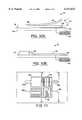
- FIG. 1is a perspective view of a corner-cube retroreflector having electrostatic plates in accordance with the present invention, wherein the electrostatic plates are shown in a substantially flat or planar position.
- FIG. 2Ais an elevational view of an electrostatic plate in a flat or planar position.
- FIG. 2Bis an elevational view of the electrostatic plate of FIG. 2A in a curled position.
- FIG. 3is a perspective view of the corner-cube retroreflector of FIG. 1, wherein the electrostatic plates are in a raised position as illustrated in FIG. 2B.
- FIG. 4is a perspective view of a corner-cube retroreflector having plates disposed in a non-regular pattern on one or more reflective surfaces thereof
- FIG. 5is an elevational view of an electrostatic plate showing varying degrees of actuation.
- FIG. 6is a cross-sectional view of a horn retroreflector having electrostatic plates in accordance with the present invention.
- FIG. 7is a perspective view of a parabolic retroreflector having electrostatic plates in accordance with a present invention.
- FIG. 8is a perspective view of a corner-cube retroreflector having electrostatic plates in accordance with a present invention, and further including electronic devices on the reflected surfaces thereof
- FIG. 9is a perspective view of a beam structure in accordance with the present invention.
- FIG. 10Ais an elevational view of the beam structure of FIG. 9 in a non-planar position.
- FIG. 10Bis an elevational view of the beam structure of FIG. 9 in a planar position.
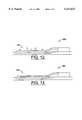
- FIG. 11is a top plan view of a group of beam structures which are collectively configured to form a reflective surface in accordance with the present invention.
- FIG. 12is a cross-sectional view taken along line 12'--12' of FIG. 11.
- FIG. 13is a cross-sectional view taken along line 13'--13' of FIG. 11.
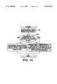
- FIG. 14is a flow chart of the operation of the corner-cube retroreflector of FIG. 8 in accordance with the present invention.
- the corner-cube retroreflector 10comprises a first microelectronic, substrate 14, a second microelectronic substrate 16, and a third microelectronic substrate 18.
- the microelectronic substrates 14, 16, and 18are interconnected to form a microelectronic retroreflector as shown. Though the microelectronic substrates 14, 16, and 18 maybe interconnected by a number of different methods as will be recognized by those skilled in the art, a preferred method is using the arch solder interconnect technique.
- an arch solder interconnect techniqueincludes the formation of a plurality of solder bumps along an edge of a first substrate which is then positioned adjacent to a second substrate.
- the solder bumpsare expanded by reflowing additional solder into the plurality of solder bumps so that the solder bumps become superhemispherical and contact the second substrate forming the arch solder interconnect.
- the additional soldermay be provided from an elongated, narrow solder-containing region adjacent into the solder bump. Surface tension from the elongated solder-containing region causes the solder to flow from the elongated solder-containing region into the solder bump, thereby expanding the volume of the solder bump causing it to expand to and contact the second substrate.
- microelectronic substrates 14, 16, 18are shown as substantially square or rectangular, those skilled in the art will recognized that the microelectronic substrates 14, 16, 18 can have other shapes such as triangles so as to form a pyramid for frustum structure. Alternative configurations of the microelectronic substrates 14, 16, and 18 may be advantageous for improving the packaging or mounting of the corner-cube retroreflector 10.
- the corner-cube retroreflector 10is configured to receive an incident radiation signal 20 and produce a reflected radiation signal 22 directed substantially parallel to the incident radiation signal 20.
- the reflected radiation signal 22is reflected back in the direction from whence it came.
- thistypically entails the incident radiation signal 20 being reflecting off two or more surfaces that have a combine reflected angle of approximately 180°. Therefore, a substantial portion of the incident radiation signal is returned to its source with the same general characteristics and relatively little spreading or scattering.
- retroreflectorssuch as the corner-cube retroreflector 10 are self-aligning, such that regardless of the incident angle of the radiation signal 20, the reflected radiation signal 22 is substantially parallel thereto.
- the electrostatic plates 12are provided on a portion of the substrate IS of the corner-cube retroreflector 10, as shown in FIG. 1.
- the electrostatic plates 12are provided to selectively introduce discontinuity in the reflective surface 24, thereby causing attenuation in the reflected radiation signal which essentially reduces the amount or strength of the incident radiation signal that is reflected back to the source of the radiation.
- the electrostatic plates 12are substantially flat (or planar) as illustrated in FIG. 2A. In this position, as also illustrated in FIG. 1, the electrostatic plates 12 do not introduce any significant amount of discontinuity into the reflective surface 24. Thus, the corner-cube retroreflector 10 operates as though the electrostatic plates 12 were not present, and substantially all the incident radiation 20 is reflected back to its source.
- the electrostatic platesare curled away from the reflective surface 24, as illustrated in FIG. 2B.
- the electrostatic plates 12introduce discontinuity in the reflective surface 24 which causes scattering of the incident radiation signal 20, as shown in FIG. 3.
- the incident radiation 20may be reflected back toward the radiation source as indicated by signal R1, and a portion of the incident radiation 20 is scattered as indicated by signal R2.
- the resultant scatteringattenuates the reflected signal R1, and thus, only a portion of the incident radiation signal is reflected back to its source.
- corner-cube retroreflector 10is designed to reflect the incident radiation back towards its source
- other reflectors in accordance with the present inventionmay be designed to reflect the incident radiation signal in a predetermined direction not toward its source.
- the radiation signal incident such a reflectormay be selectively scattered so that only a portion of the incident signal is reflected in the predetermined direction. This substantially equivalent to the operation of the corner-cube retroreflector described herein, and is within the scope of the present invention.
- the electrostatic plate 12can be formed in the microelectronic substrate 18 utilizing microelectromechanical systems (MEMs) technology.
- MEMsmicroelectromechanical systems
- a plate member 30can be formed by depositing and patterning a thin polysilicon conductive layer 32 on a substrate for operating as a lower electrode. A sacrificial layer of oxide may then deposited over the lower electrode 32 and a polysilicon layer deposited thereover. The polysilicon layer is then patterned and etched to form the plate member 30. The plate member 30 is released by removing the sacrificial layer of oxide. A metal layer 34 (preferable titanium or chromium) that is tensile in nature is deposited and patterned over the plate member 30.
- the residual stress distribution from the composite bilayer constructionwill cause the plate member 30 to curl away from or move relative to the reflective surface 24, as shown in FIG. 2B.
- the plate member 30is curled away from the substrate 18.
- the plate member 30By placing a pre-determined voltage charge on the lower electrode 32 via an actuation mechanism 36 such as a microprocessor, the plate member 30 is drawn toward the lower electrode 32 such that the plate member 30 is substantially flat in its fully actuated state, as shown in FIG. 2A.
- actuation mechanism 36such as a microprocessor
- a voltage charge of approximately less than 150 voltsshould be sufficient to fully actuate a plate 2 microns thick, and 20 microns wide.
- electrostatic plates 12 described hereinare rectangular in shape, it will be understood by those skilled in the art that the electrostatic plates may take other regular shapes such as triangular, circular, polygonal, or virtually any regular or nonregular shape. Further, methods of actuating the plate members other than electrostatically may be utilized in accordance with the present invention. For example, the plate members may be thermally actuated using thermal bimorphs or shape memory alloys.
- thermally actuated platescan be found, for example, in Manabu Ataka, et al., "A Biomimetic Micro Motion System--A Ciliary Motion System," The 7th International Conference on Solid-State Sensors and Actuators-Transducers '93, Yokohama, Japan, June, 1993, pp. 38-41 (ISBN 4-9900247-2-9).
- one type of thermally actuated platemay comprise a heater layer sandwiched between two polymer layers, wherein the polymer layers have different coefficient of thermal expansion so that the plate curls when heated. The curl is generally in the direction of the layer having the higher coefficient of thermal expansion.
- the heaterpreferably comprises a metallic layer of gold and/or nickel.
- the plateBy passing a current in the heater layer, the plate uncurls and becomes substantially planar.
- the platemay be electromagnetically actuated.
- coilscan be integrated in the substrate opposite the plaite, and the plate may include a magnetic material. The plate members can then be deformed by passing a current through the coil which creates an electric filed that may either attract or repel the plate member so as to deform the plate.
- datacan be encoded on the reflected radiation signal using a variety of modulation schemes such as amplitude modulation, phase modulation, or frequency modulation. For instance, if the incident radiation signal is a direct current (DC) signal, then the plate member; 30 can be actuated in time so that the reflected radiation signal oscillates between essentially two power levels. Thus, binary data may be encoded on the reflected radiation signal.
- DCdirect current
- the electrostatic plates 12 described abovecan achieve modulation frequencies in the kilohertz range.
- An inhibitor to even higher frequency operationis air dampening or resistance.
- the problem of air dampeningmay be reduced by fabricating narrower plate members 30, and/or fabricating ventilation holes through the plate members 310.
- the structurecan be fabricated in a vacuum package that is hermetically sealed to substantially eliminate the problem of air dampening when actuating; the electrostatic plates.
- the amount of attenuation imposed upon the incident radiation signalcan be controlled.
- the attenuationcan be controlled by the amount of the reflective surface(s) that is covered by the electrostatic plates. If only a small portion of the reflective surface is covered by one or more electrostatic plate, then a corresponding portion of the incident radiation signal is scattered when the electrostatic plates are in a curled position (i.e., an unactuated position as illustrated in FIG. 2B).
- a correspondingly larger portion of the incident radiation signalis scattered, and therefore, less of the incident radiation signal is reflected back by the retroreflector.
- the characteristics of the reflected radiation signalcan be partially controlled by designing a retroreflector having a defined portion of its reflective surface(s) covered by electrostatic plates. If a sufficient portion of the reflective surface(s) is covered by electrostatic plates, then substantially all of the incident radiation signal may be scattered and essentially none of the radiation signal will be reflected back to the radiation source. Such a configuration may be particularly advantageous in certain applications such as in a battlefield where it may be desirable not to reflect any of the incident radiation beam until verification can be made that the incident beam is from a friendly interrogation unit.
- the electrostatic platesmay be disposed in a non-regular pattern on one or more reflective surfaces of the comer-cube retroreflector, as illustrated in FIG. 4.
- the non-regular pattern of the electrostatic plates on the corner-cube retroreflector 40is less likely to produce a recognizable reflection when the electrostatic plates are in a curled position, which may prevent the reflection from being detected as a recognizable signal. This may be particularly advantageous when the corner-cube retroreflector 40 is being used in IFF tasks, wherein the retroreflector 40 is mounted on a targeted object that does not want to reflect a radiation signal having a distinguishable signature that may be identified by unfriendly forces. Therefore, the electrostatic plates may be configured in a non-regular pattern as shown in FIG. 4 so that any reflected radiation is substantially random in nature. Furthermore, the individual electrostatic plates can be selectively actuated to further increase the randomness of the reflected radiation.
- the individual plate members 30can be partially actuated to introduce a controllable degree of discontinuity in the reflective surface 24.
- the plate member 30may be drawn toward the substrate 18 in varying degrees by applying a variable actuation voltage to the lower electrode 32.
- the plateIn a first position 50, the plate is in an unactuated position and is significantly curled away from the reflective surface 24.
- the plateIn a second position 52, the plate is partially actuated and the electrostatic pull of the lower electrode 32 draws the plate member 30 toward the reflective surface 24, and thereby, may cause less scattering of the incident radiation than when in position 50.
- a third position 54the plate is partially actuated to a greater degree than position 52, drawing plate member 30 relatively closer to the reflective surface 24, and thereby, may cause even less scattering than when in position 52. Accordingly, by selectively controlling the degree of actuation (i.e., the amount of curl of plate member 20), the scattering caused by an electrostatic late can be controlled.
- the degree of actuationi.e., the amount of curl of plate member 20
- a plurality of electrostatic membersan be individually actuated at varying degrees in order to further increase the andomness with which the incident radiation signal is scattered, and to decrease the signature of the reflection.
- FIG. 6shown is a horn retroreflector 60 incorporating electrostatic plates 62 in accordance with the present invention. It is noted that the electrostatic plates 62 also can be located on a curved surface 64 of the horn reitroreflector 60. In another configuration, as illustrated in FIG. 7, a parabolic retroreflector 70 incorporates the electrostatic plates 72 on the reflector surface 74.
- the retroreflectors of FIGS. 6 and 7may operate in substantially the same manner as the corner-cube retroreflector 10 described above.
- the electrostatic plateswhen actuated, may reflect a substantial portion of the incident radiation so that the retroreflec;tors operate as intended, that is, a substantial portion of the reflective radiation signal is directed back in the direction from whence it came.
- the electrostatic platesWhen in an unactuated state, the electrostatic plates scatter the incident radiation so that a relatively smaller portion of the incident radiation is reflected back in the direction from whence it came.
- a corner-cube retroreflector 80incorporating electrostatic plates 82 in accordance with the present invention and microelectronic devices such as emitters/detectors 84 disposed on the surfaces of the corner-cube retroreflector 80.
- the microelectronic devicesmay be memory devices, microprocessors, drivers, or other conventional microelectronic circuitry.
- the corner-cube retroreflector 80may include a centrally located microelectronic device such as a detector/emitter 86 positioned at the apex of the cornercube retroreflector 80.
- the emitters/detectors 84, 86may be configured to operate in a particular frequency range so as to limit the bandwidth of sensitivity.
- emitter/detectors 84, 86may be radio transmitters, radio receivers, laser diodes, or light emitting diodes (LEDs).
- the incident radiation signalmay be received and processed by associated systems for determining if or what reflective signal would be appropriate.
- additional signalsmay be transmitted in a predetermined direction, or alternatively, the emitter may provide other particular functionalities as may be desirable.
- a plate 12is one embodiment of a deformable structure in accordance with the present invention for introducing discontinuity in a reflective surface
- other means suitable for selectively altering the reflectivity of a reflectormay be utilized.
- a beammay be utilized.
- the beammay be rigidly mounted at one or more edges, and may be actuated in substantially the same manner as the plate embodiment.
- An illustrative embodiment of a beam in accordance with the present inventionis described below.
- a beam structure 92comprises a reflective plate 94 that is attached to a substrate 104 by a substrate connection 96 in at least one location.
- An actuation mechanism 102is preferably integrated in the substrate 104.
- the reflective plate 94preferably comprises polysilicon with controlled residual stress so that the reflective plate 94 is substantially non-planar.
- the reflective plate 94may include a curl or bend 106 which operates to scatter, in an incoherent manner, the radiation incident the beam structure 92.
- the reflective plate 94may be rigidly planar as compared to the substrate connection 96 which may contain residual stress, and therefore, the deformation of the beam structure 92 may primarily take place at the substrate connection 96.
- the beam structure 94can be actuated by numerous methods including electrostatically, thermally or magnetically.
- the beam structureis electrostatically activated.
- implementation of a thermally or magnetically actuated beam structurecan be achieved in substantially the same manner as a thermally or magnetically actuated plate, as described above and as will be appreciated by those skilled in the art.
- the actuation mechanism 102comprises an electrode 107 that can be selectively charged to create an electrostatic force for attracting the reflective plate 94 to the substrate 104, as illustrated in FIGS. 10A and 10B.
- the reflective plate 94is preferably positioned at least 100 nanometer from the substrate 104, as represented by reference numeral 108.
- the separation distance 108will be a major determinant of the necessary actuation voltage, and can be tailored to suit the operational need of the device.
- the reflective plate 94preferably includes a curl or bend 106 with a radius of curvature between 10 centimeters and 1 meter.
- the amount of curl 106should be large enough to scatter of the incident radiation, but as small as possible so as to reduce the voltage necessary to deform the reflective plate 94 into the position shown in FIG. 10B.
- engineering the amount curl 110 and the distance 108may reduce the power consumption and increase the efficiency of the beam structure 92.
- Another determinant to be considered in the designis the trade-off between providing a larger reflecting surface area, while minimizing the voltage necessary to actuate the beam or plate.
- the respective beam structurescan be individually actuated as may be desired to produce a distinctive reflected signal.
- the frequency of the encoded reflected signal and the power consumption of the beam structuresmight be improved by utilizing smaller beam structures to create a larger collective reflective surface or area.
- the reflective surfaces of the respective beam structures 92a-92c of FIG. 1Iinclude illustrative examples of threedimensional patterns 122 for passively encoding data onto a reflected signal, much like a barcode pattern.
- the three-dimensional patterns 122may comprise projections fabricated on the reflective surface as illustrated in FIG. 12, or indentions (i.e., holes) whether filled or left empty, integrated in the reflected surfaces as illustrated in FIG. 13.
- the projections and indentionscan be fabricated using MEMS technology as is known to those skilled in the art.
- the structures comprising the three-dimensional pattern 122may have optical characteristics different than that of the reflective surface of the respective beam structures.
- one methodmay comprise a series of gold structures that are produced on the reflecting surface through the use of a polymer plating template and electroplated gold. Those skilled in the art will recognize that there are numerous other methods by which these three-dimensional patterns can be formed.
- each beam structuremay be individually actuated into either an "off" or “on” mode (i.e., actuated or unactuated position). In this position, each beam structure is capable of reflecting an incident radiation signal in a distinctive manner so as to encode a specific message to the recipient of a reflected signal.
- four beam structurescan encode at least four distinctive messages onto a reflected signal. This not only reduces the logic necessary to create a data message, but it also reduces the energy necessary for encoding the data since the beam structure does not have to be modulated in a repetitive fashion.
- the electrostatic plates 82 of the cornercube retroreflector 80are initially in a normal, unactuated position such that only a small portion, if any, of a radiation signal is reflected back to the radiation source.
- the appropriate processing of the received incident radiation signaldetermines whether the electrostatic plates 82 should be actuated so as to respond to the incident radiation signal, as indicated by block 132.
- the corner-cube retroreflector 80selectively mechanically deforms a portion of the reflective surface by actuating one or more plate members to selectively reflect a portion of the incident radiation signal as indicated by block 134.
- the plate memberremains in a normal, unactuated position, as indicated by block 136.
- one or more of the emitters/detectors 84, 86may emit a radiation signal which can be received by the source of the incident radiation signal.
- the retroreflector structures described hereincan be manufactured using microelectronic substrates, it is noted that electronic circuitry for driving or controlling the operation of the electrostatic plates and/or the emitter/detectors can be fabricated on the microelectronic substrates comprising the retroreflector. Furthermore the emitter/detectors may be mounted to the microelectronic substrates in a variety of known methods including Surface Mount Technology (SMT) through-hole, flip-chip and Multi-chip Module (MCM) constructions.
- SMTSurface Mount Technology
- MCMMulti-chip Module
Landscapes
- Physics & Mathematics (AREA)
- Engineering & Computer Science (AREA)
- Remote Sensing (AREA)
- Radar, Positioning & Navigation (AREA)
- General Physics & Mathematics (AREA)
- Electromagnetism (AREA)
- Computer Networks & Wireless Communication (AREA)
- Optics & Photonics (AREA)
- Plasma & Fusion (AREA)
- Mechanical Light Control Or Optical Switches (AREA)
- Aerials With Secondary Devices (AREA)
- Optical Elements Other Than Lenses (AREA)
- Radar Systems Or Details Thereof (AREA)
- Optical Radar Systems And Details Thereof (AREA)
Abstract
Description
Claims (30)
Priority Applications (7)
| Application Number | Priority Date | Filing Date | Title |
|---|---|---|---|
| US09/042,836US6137623A (en) | 1998-03-17 | 1998-03-17 | Modulatable reflectors and methods for using same |
| AU31067/99AAU3106799A (en) | 1998-03-17 | 1999-03-16 | Modulatable reflectors and methods for using same |
| EP99912763AEP1064571A2 (en) | 1998-03-17 | 1999-03-16 | Modulatable reflectors and methods for using same |
| KR1020007010295AKR20010041970A (en) | 1998-03-17 | 1999-03-16 | Modulatable reflectors and methods for using same |
| JP2000537092AJP4458665B2 (en) | 1998-03-17 | 1999-03-16 | Modulatable reflector and method for using the same |
| PCT/US1999/006152WO1999047950A2 (en) | 1998-03-17 | 1999-03-16 | Modulatable reflectors and methods for using same |
| US09/636,141US6233088B1 (en) | 1998-03-17 | 2000-08-10 | Methods for modulating a radiation signal |
Applications Claiming Priority (1)
| Application Number | Priority Date | Filing Date | Title |
|---|---|---|---|
| US09/042,836US6137623A (en) | 1998-03-17 | 1998-03-17 | Modulatable reflectors and methods for using same |
Related Child Applications (1)
| Application Number | Title | Priority Date | Filing Date |
|---|---|---|---|
| US09/636,141DivisionUS6233088B1 (en) | 1998-03-17 | 2000-08-10 | Methods for modulating a radiation signal |
Publications (1)
| Publication Number | Publication Date |
|---|---|
| US6137623Atrue US6137623A (en) | 2000-10-24 |
Family
ID=21924006
Family Applications (2)
| Application Number | Title | Priority Date | Filing Date |
|---|---|---|---|
| US09/042,836Expired - LifetimeUS6137623A (en) | 1998-03-17 | 1998-03-17 | Modulatable reflectors and methods for using same |
| US09/636,141Expired - LifetimeUS6233088B1 (en) | 1998-03-17 | 2000-08-10 | Methods for modulating a radiation signal |
Family Applications After (1)
| Application Number | Title | Priority Date | Filing Date |
|---|---|---|---|
| US09/636,141Expired - LifetimeUS6233088B1 (en) | 1998-03-17 | 2000-08-10 | Methods for modulating a radiation signal |
Country Status (6)
| Country | Link |
|---|---|
| US (2) | US6137623A (en) |
| EP (1) | EP1064571A2 (en) |
| JP (1) | JP4458665B2 (en) |
| KR (1) | KR20010041970A (en) |
| AU (1) | AU3106799A (en) |
| WO (1) | WO1999047950A2 (en) |
Cited By (29)
| Publication number | Priority date | Publication date | Assignee | Title |
|---|---|---|---|---|
| US6233088B1 (en)* | 1998-03-17 | 2001-05-15 | Mcnc | Methods for modulating a radiation signal |
| US6300619B1 (en)* | 1997-12-22 | 2001-10-09 | Lucent Technologies Inc. | Micro-electro-mechanical optical device |
| US6299462B1 (en)* | 1999-11-15 | 2001-10-09 | Xerox Corporation | Self positioning, passive MEMS mirror structures |
| US6392221B1 (en)* | 1997-12-22 | 2002-05-21 | Agere Systems Guardian Corp. | Micro-electro-mechanical optical device |
| US20030002738A1 (en)* | 2001-07-02 | 2003-01-02 | Trw Inc. | Vehicle occupant sensor apparatus and method including scanned, phased beam transmission for occupant characteristic determination |
| EP1341025A1 (en)* | 2002-03-01 | 2003-09-03 | Microsoft Corporation | Reflective microelectrical mechanical structure (mems) optical modulator and optical display system |
| US20030184189A1 (en)* | 2002-03-29 | 2003-10-02 | Sinclair Michael J. | Electrostatic bimorph actuator |
| US20040125432A1 (en)* | 2002-01-09 | 2004-07-01 | Tohru Ishizuya | Optical element, thin film structure, optical switch, and method of manufacturing optical element |
| WO2004056547A2 (en) | 2002-12-20 | 2004-07-08 | Koninklijke Philips Electronics N.V. | Micro-mechanical thermo structure and method for manufacturing such micro-mechanical structure |
| US20040233498A1 (en)* | 2000-10-31 | 2004-11-25 | Microsoft Corporation | Microelectrical mechanical structure (MEMS) optical modulator and optical display system |
| US20040252005A1 (en)* | 2003-06-10 | 2004-12-16 | The Boeing Company | Shape memory alloy MEMS component deposited by chemical vapor deposition |
| US20050011191A1 (en)* | 2001-12-31 | 2005-01-20 | Microsoft Corporation | Unilateral thermal buckle beam actuator |
| US20050099261A1 (en)* | 2003-11-06 | 2005-05-12 | Steven Walak | Two way composite nitinol actuation |
| US20050105153A1 (en)* | 2003-11-18 | 2005-05-19 | Youngner Daniel W. | Dynamic reflector array and method of making the same |
| US20050105914A1 (en)* | 2003-11-17 | 2005-05-19 | Chen Chungte W. | Method for identifying an interrogated object using a dynamic optical tag identification system |
| RU2254596C2 (en)* | 2003-08-11 | 2005-06-20 | ОАО "Уральское проектно-конструкторское бюро "Деталь" | System of identification of mobile objects |
| US20050135812A1 (en)* | 2003-12-18 | 2005-06-23 | Pease David M. | Laser-based communications with a remote information source |
| WO2005075605A1 (en)* | 2004-02-04 | 2005-08-18 | Koninklijke Philips Electronics N.V. | Flexible foil moveable by non-mechanical means |
| US20060072224A1 (en)* | 2000-04-07 | 2006-04-06 | Microsoft Corporation | Magnetically actuated microelectromechanical systems actuator |
| US20060072079A1 (en)* | 2004-10-06 | 2006-04-06 | Lg Electronics Inc | Projection display system with micro-mirror light modulator |
| US7249859B1 (en)* | 2003-12-18 | 2007-07-31 | United States Of America As Represented By The Secretary Of The Navy | Corner cube chemical-biological agent sensor |
| US20080030828A1 (en)* | 2006-08-07 | 2008-02-07 | Samsung Electronics Co., Ltd. | Display device and method of manufacturing the same |
| US20090128589A1 (en)* | 2007-11-19 | 2009-05-21 | Microsoft Corporation | Display device and pixel therefor |
| US8224189B1 (en) | 2007-02-02 | 2012-07-17 | Sunlight Photonics Inc. | Retro-directive target for free-space optical communication and method of producing the same |
| RU2543514C2 (en)* | 2013-07-15 | 2015-03-10 | Российская Федерация, от имени которой выступает Министерство обороны Российской Федерации | Formation method of signals and information transmission in backward channel of radar identification system |
| WO2018039558A1 (en) | 2016-08-26 | 2018-03-01 | Filo Andrew Simon | Modulating retroreflective piezoelectric multilayer film |
| WO2020088755A1 (en)* | 2018-10-31 | 2020-05-07 | Nokia Technologies Oy | Apparatus for Reflecting Electromagnetic Waves and Method of Operating such Apparatus |
| US11630207B2 (en) | 2017-06-28 | 2023-04-18 | Mitsubishi Heavy Industries, Ltd. | Flying body |
| EP4415174A1 (en)* | 2023-02-08 | 2024-08-14 | Siemens Aktiengesellschaft | A communication system for wireless transmitting a data signal from a transmission device of the communication system to at least a first receiving device of the communication system |
Families Citing this family (19)
| Publication number | Priority date | Publication date | Assignee | Title |
|---|---|---|---|---|
| US6535318B1 (en)* | 1999-11-12 | 2003-03-18 | Jds Uniphase Corporation | Integrated optoelectronic devices having pop-up mirrors therein and methods of forming and operating same |
| US6456420B1 (en)* | 2000-07-27 | 2002-09-24 | Mcnc | Microelectromechanical elevating structures |
| US7035546B2 (en)* | 2000-09-20 | 2006-04-25 | Texas Instruments Incorporated | Optical wireless multiport hub |
| US6586738B2 (en) | 2001-04-13 | 2003-07-01 | Mcnc | Electromagnetic radiation detectors having a micromachined electrostatic chopper device |
| US7026602B2 (en)* | 2001-04-13 | 2006-04-11 | Research Triangle Institute | Electromagnetic radiation detectors having a microelectromechanical shutter device |
| US6669145B1 (en) | 2002-12-30 | 2003-12-30 | The Boeing Company | Apparatus, method and system for fluid-motion-powered modulation of a retroreflector for remote position sensing |
| US7112463B2 (en) | 2003-11-13 | 2006-09-26 | Honeywell International Inc. | Method for making devices using ink jet printing |
| WO2005086585A2 (en)* | 2004-03-15 | 2005-09-22 | Iralink Ltd | Retromodulation-based data communication |
| US7484857B2 (en)* | 2004-11-30 | 2009-02-03 | Massachusetts Institute Of Technology | Light modulating mirror device and array |
| SE528004C2 (en)* | 2004-12-17 | 2006-08-01 | Totalfoersvarets Forskningsins | Device for optical remote listening and systems including such device |
| US7950812B2 (en) | 2006-01-11 | 2011-05-31 | Cubic Corporation | Shutters for infra red communication at moderate bandwidths |
| DE102008009215A1 (en)* | 2008-02-13 | 2009-08-20 | Universität Kassel | Component for displaying symbols and optical display device produced therewith |
| JP2009258511A (en)* | 2008-04-18 | 2009-11-05 | Toyota Central R&D Labs Inc | Optical element and optical device |
| US8023175B2 (en)* | 2009-02-06 | 2011-09-20 | The United States Of America As Represented By The Secretary Of The Army | Dynamic imaging and/or identification apparatus and method thereof |
| KR101041886B1 (en)* | 2009-10-14 | 2011-06-15 | 국방과학연구소 | Corner cube retroreflector and its manufacturing method |
| JP2016151496A (en)* | 2015-02-18 | 2016-08-22 | ローム株式会社 | Position detection device, electric apparatus using the same, and position detection method |
| US10222265B2 (en)* | 2016-08-19 | 2019-03-05 | Obsidian Sensors, Inc. | Thermomechanical device for measuring electromagnetic radiation |
| US10908328B2 (en)* | 2016-09-20 | 2021-02-02 | Apple Inc. | Retroreflectors |
| JPWO2020044411A1 (en)* | 2018-08-27 | 2021-08-10 | 光トライオード株式会社 | Laser beam search system |
Citations (27)
| Publication number | Priority date | Publication date | Assignee | Title |
|---|---|---|---|---|
| US3917196A (en)* | 1974-02-11 | 1975-11-04 | Boeing Co | Apparatus suitable for use in orienting aircraft flight for refueling or other purposes |
| US4025193A (en)* | 1974-02-11 | 1977-05-24 | The Boeing Company | Apparatus suitable for use in orienting aircraft in-flight for refueling or other purposes |
| US4143946A (en)* | 1977-12-05 | 1979-03-13 | The United States Of America As Represented By The Secretary Of The Navy | Impingement cooled deformable laser mirror |
| US4209689A (en)* | 1969-06-04 | 1980-06-24 | Hughes Aircraft Company | Laser secure communications system |
| US4361911A (en)* | 1981-05-21 | 1982-11-30 | The United States Of American As Represented By The Secretary Of The Army | Laser retroreflector system for identification of friend or foe |
| DE3230159C1 (en)* | 1982-08-13 | 1983-04-07 | Messerschmitt-Bölkow-Blohm GmbH, 8000 München | Piezoelectrically excitable cube-corner retroreflector |
| GB2123248A (en)* | 1982-07-02 | 1984-01-25 | Xerox Corp | Dual mode facsimile apparatus |
| US4447723A (en)* | 1981-09-03 | 1984-05-08 | Excellon Industries | Scanning beam reference employing a retroreflective code means |
| US4517569A (en)* | 1982-02-17 | 1985-05-14 | The United States Of America As Represented By The Secretary Of The Army | Passive retroreflective doppler shift system |
| US4727593A (en)* | 1981-03-25 | 1988-02-23 | Pinchas Goldstein | Passive line-of-sight optical switching apparatus |
| US4731869A (en)* | 1985-02-18 | 1988-03-15 | Plessey Overseas Limited | Target tracking transmitter having two levels of power operation |
| US4762426A (en)* | 1986-12-19 | 1988-08-09 | Honeywell Inc. | Remote passive temperature sensor |
| US4777660A (en)* | 1984-11-06 | 1988-10-11 | Optelecom Incorporated | Retroreflective optical communication system |
| US4887310A (en)* | 1986-08-01 | 1989-12-12 | Thomson Csf | Identification system using a laser retro-reflecting and modulating set |
| US4983021A (en)* | 1988-08-10 | 1991-01-08 | Fergason James L | Modulated retroreflector system |
| US5274379A (en)* | 1991-11-08 | 1993-12-28 | Her Majesty The Queen As Represented By The Minister Of National Defence Of Her Majesty's Canadian Government | Optical identification friend-or-foe |
| US5311360A (en)* | 1992-04-28 | 1994-05-10 | The Board Of Trustees Of The Leland Stanford, Junior University | Method and apparatus for modulating a light beam |
| US5355241A (en)* | 1991-12-09 | 1994-10-11 | Kelley Clifford W | Identification friend or foe discriminator |
| CA2094174A1 (en)* | 1993-04-16 | 1994-10-17 | Raja Singh Tuli | Miniature high resolution viewscreen cantilever i.c. |
| US5438449A (en)* | 1987-11-25 | 1995-08-01 | Raytheon Company | Beam pointing switch |
| WO1995023352A1 (en)* | 1994-02-23 | 1995-08-31 | Aura Systems, Inc. | Thin film actuated mirror array |
| US5568307A (en)* | 1995-02-07 | 1996-10-22 | Mcdonnell Douglas Corporation | Apparatus for controlling the reflectance of an object surface |
| US5583507A (en)* | 1995-04-19 | 1996-12-10 | Martin Marietta Corporation | Passive identification of friend vs. foe apparatus and method |
| GB2307762A (en)* | 1995-11-28 | 1997-06-04 | George Stylios | Bar codes |
| US5661592A (en)* | 1995-06-07 | 1997-08-26 | Silicon Light Machines | Method of making and an apparatus for a flat diffraction grating light valve |
| EP0807841A2 (en)* | 1996-05-13 | 1997-11-19 | Lucent Technologies Inc. | Improved optical modulator/switch |
| US5757562A (en)* | 1996-01-31 | 1998-05-26 | Compagnie Industrielle Des Lasers Cilas | Mirror with reflection coefficient variable spatially in amplitude and in phase |
Family Cites Families (10)
| Publication number | Priority date | Publication date | Assignee | Title |
|---|---|---|---|---|
| US3886310A (en)* | 1973-08-22 | 1975-05-27 | Westinghouse Electric Corp | Electrostatically deflectable light valve with improved diffraction properties |
| DE3328335C2 (en) | 1983-08-05 | 1987-01-22 | Messerschmitt-Bölkow-Blohm GmbH, 8012 Ottobrunn | Remote data monitoring system |
| US5072239A (en)* | 1989-12-21 | 1991-12-10 | Texas Instruments Incorporated | Spatial light modulator exposure unit and method of operation |
| US5159498A (en)* | 1990-03-01 | 1992-10-27 | The Charles Stark Draper Laboratory, Inc. | Active mirror assembly |
| US5966230A (en)* | 1990-05-29 | 1999-10-12 | Symbol Technologies, Inc. | Integrated scanner on a common substrate |
| US5233459A (en)* | 1991-03-06 | 1993-08-03 | Massachusetts Institute Of Technology | Electric display device |
| JP3092989B2 (en)* | 1991-08-20 | 2000-09-25 | 俊弘 津村 | Light modulator |
| US5221987A (en)* | 1992-04-10 | 1993-06-22 | Laughlin Richard H | FTIR modulator |
| US6137623A (en)* | 1998-03-17 | 2000-10-24 | Mcnc | Modulatable reflectors and methods for using same |
| US6057520A (en)* | 1999-06-30 | 2000-05-02 | Mcnc | Arc resistant high voltage micromachined electrostatic switch |
- 1998
- 1998-03-17USUS09/042,836patent/US6137623A/ennot_activeExpired - Lifetime
- 1999
- 1999-03-16AUAU31067/99Apatent/AU3106799A/ennot_activeAbandoned
- 1999-03-16EPEP99912763Apatent/EP1064571A2/ennot_activeWithdrawn
- 1999-03-16KRKR1020007010295Apatent/KR20010041970A/ennot_activeWithdrawn
- 1999-03-16JPJP2000537092Apatent/JP4458665B2/ennot_activeExpired - Fee Related
- 1999-03-16WOPCT/US1999/006152patent/WO1999047950A2/ennot_activeApplication Discontinuation
- 2000
- 2000-08-10USUS09/636,141patent/US6233088B1/ennot_activeExpired - Lifetime
Patent Citations (27)
| Publication number | Priority date | Publication date | Assignee | Title |
|---|---|---|---|---|
| US4209689A (en)* | 1969-06-04 | 1980-06-24 | Hughes Aircraft Company | Laser secure communications system |
| US3917196A (en)* | 1974-02-11 | 1975-11-04 | Boeing Co | Apparatus suitable for use in orienting aircraft flight for refueling or other purposes |
| US4025193A (en)* | 1974-02-11 | 1977-05-24 | The Boeing Company | Apparatus suitable for use in orienting aircraft in-flight for refueling or other purposes |
| US4143946A (en)* | 1977-12-05 | 1979-03-13 | The United States Of America As Represented By The Secretary Of The Navy | Impingement cooled deformable laser mirror |
| US4727593A (en)* | 1981-03-25 | 1988-02-23 | Pinchas Goldstein | Passive line-of-sight optical switching apparatus |
| US4361911A (en)* | 1981-05-21 | 1982-11-30 | The United States Of American As Represented By The Secretary Of The Army | Laser retroreflector system for identification of friend or foe |
| US4447723A (en)* | 1981-09-03 | 1984-05-08 | Excellon Industries | Scanning beam reference employing a retroreflective code means |
| US4517569A (en)* | 1982-02-17 | 1985-05-14 | The United States Of America As Represented By The Secretary Of The Army | Passive retroreflective doppler shift system |
| GB2123248A (en)* | 1982-07-02 | 1984-01-25 | Xerox Corp | Dual mode facsimile apparatus |
| DE3230159C1 (en)* | 1982-08-13 | 1983-04-07 | Messerschmitt-Bölkow-Blohm GmbH, 8000 München | Piezoelectrically excitable cube-corner retroreflector |
| US4777660A (en)* | 1984-11-06 | 1988-10-11 | Optelecom Incorporated | Retroreflective optical communication system |
| US4731869A (en)* | 1985-02-18 | 1988-03-15 | Plessey Overseas Limited | Target tracking transmitter having two levels of power operation |
| US4887310A (en)* | 1986-08-01 | 1989-12-12 | Thomson Csf | Identification system using a laser retro-reflecting and modulating set |
| US4762426A (en)* | 1986-12-19 | 1988-08-09 | Honeywell Inc. | Remote passive temperature sensor |
| US5438449A (en)* | 1987-11-25 | 1995-08-01 | Raytheon Company | Beam pointing switch |
| US4983021A (en)* | 1988-08-10 | 1991-01-08 | Fergason James L | Modulated retroreflector system |
| US5274379A (en)* | 1991-11-08 | 1993-12-28 | Her Majesty The Queen As Represented By The Minister Of National Defence Of Her Majesty's Canadian Government | Optical identification friend-or-foe |
| US5355241A (en)* | 1991-12-09 | 1994-10-11 | Kelley Clifford W | Identification friend or foe discriminator |
| US5311360A (en)* | 1992-04-28 | 1994-05-10 | The Board Of Trustees Of The Leland Stanford, Junior University | Method and apparatus for modulating a light beam |
| CA2094174A1 (en)* | 1993-04-16 | 1994-10-17 | Raja Singh Tuli | Miniature high resolution viewscreen cantilever i.c. |
| WO1995023352A1 (en)* | 1994-02-23 | 1995-08-31 | Aura Systems, Inc. | Thin film actuated mirror array |
| US5568307A (en)* | 1995-02-07 | 1996-10-22 | Mcdonnell Douglas Corporation | Apparatus for controlling the reflectance of an object surface |
| US5583507A (en)* | 1995-04-19 | 1996-12-10 | Martin Marietta Corporation | Passive identification of friend vs. foe apparatus and method |
| US5661592A (en)* | 1995-06-07 | 1997-08-26 | Silicon Light Machines | Method of making and an apparatus for a flat diffraction grating light valve |
| GB2307762A (en)* | 1995-11-28 | 1997-06-04 | George Stylios | Bar codes |
| US5757562A (en)* | 1996-01-31 | 1998-05-26 | Compagnie Industrielle Des Lasers Cilas | Mirror with reflection coefficient variable spatially in amplitude and in phase |
| EP0807841A2 (en)* | 1996-05-13 | 1997-11-19 | Lucent Technologies Inc. | Improved optical modulator/switch |
Non-Patent Citations (18)
| Title |
|---|
| "A Large-Aperture Electro-Optic Diffraction Modulator", J. Appl.Phys. 50(11), Nov. 1979, pp. 6691-6693. |
| "Dry-Released Process for Aluminum Electrostatic Actuators", Christopher W. Storment et al., Solid-State Sensor and Actuator Workshop, Hilton Head, South Carolina, Jun. 13-16, 1994. |
| "Large Aperture Stark Modulated Retroreflector at 10.8 μm", M.B. Klein and R.H. Sipman, J. Appl. Phys., 51(12), Dec. 1980, pp. 1601-1604. |
| "Microwave Reflection Properties of a Rotating Corrugated Metallic Plate Used as a Reflection Modulator", Gordon E. Peckham and Robert A. Suttie, IEEE Transactions on Antennas and Propagation, vol. 36, No. 7, Jul. 1988, pp. 1000-1006. |
| A Large Aperture Electro Optic Diffraction Modulator , J. Appl.Phys . 50(11), Nov. 1979, pp. 6691 6693.* |
| Deformable Grating Light Valves for High Resolution Displays Apte et al., Ginzton Laboratory, Stanford University, Solid State Sensor and Actuator Workshop, Hilton Head, South Carolina, Jun. 13 16, 1994.* |
| Deformable Grating Light Valves for High Resolution Displays Apte et al., Ginzton Laboratory, Stanford University, Solid-State Sensor and Actuator Workshop, Hilton Head, South Carolina, Jun. 13-16, 1994. |
| Devi S. Gunawan et al., Micromachined Corner Cube Reflectors As A Communication Link, Sensors and Actuators A , vol. A47, No. 1/03, Mar. 1, 1995, pp. 580 583, XP000516324.* |
| Devi S. Gunawan et al., Micromachined Corner Cube Reflectors As A Communication Link, Sensors and Actuators A, vol. A47, No. 1/03, Mar. 1, 1995, pp. 580-583, XP000516324. |
| Dry Released Process for Aluminum Electrostatic Actuators , Christopher W. Storment et al., Solid State Sensor and Actuator Workshop, Hilton Head, South Carolina, Jun. 13 16, 1994.* |
| Large Aperture Stark Modulated Retroreflector at 10.8 m , M.B. Klein and R.H. Sipman, J. Appl. Phys ., 51(12), Dec. 1980, pp. 1601 1604.* |
| M. Edward Motamedi et al., Development of Micro Electro Mechanical Optical Scanner, Optical Engineering , vol. 36, No. 5, May 1, 1997, pp. 1346 1352, XP000692364.* |
| M. Edward Motamedi et al., Development of Micro-Electro-Mechanical Optical Scanner, Optical Engineering, vol. 36, No. 5, May 1, 1997, pp. 1346-1352, XP000692364. |
| Manabu Ataka et al., "A Biomimetic Micro Motion System--a Ciliary Motion System", The 7th International Conference on Solid-State Sensors and Actuators--Transducers '93, Yokohama, Japan, Jun., 1993, pp. 38-41 (ISBN 4-9900247-2-9). |
| Manabu Ataka et al., A Biomimetic Micro Motion System a Ciliary Motion System , The 7th International Conference on Solid State Sensors and Actuators Transducers 93, Yokohama, Japan, Jun., 1993, pp. 38 41 (ISBN 4 9900247 2 9).* |
| Microwave Reflection Properties of a Rotating Corrugated Metallic Plate Used as a Reflection Modulator , Gordon E. Peckham and Robert A. Suttie, IEEE Transactions on Antennas and Propagation , vol. 36, No. 7, Jul. 1988, pp. 1000 1006.* |
| W. Benecke, "Silicon--Microactuators: Activation Mechanisms and Scaling Problems", 1991 IEEE International Conference on Solid-State Sensors and Actuators Proceedings, San Francisco, Jun., 1991, pp. 46-49 (ISBN 0-87942-585-3). |
| W. Benecke, Silicon Microactuators: Activation Mechanisms and Scaling Problems , 1991 IEEE International Conference on Solid State Sensors and Actuators Proceedings, San Francisco, Jun., 1991, pp. 46 49 (ISBN 0 87942 585 3).* |
Cited By (71)
| Publication number | Priority date | Publication date | Assignee | Title |
|---|---|---|---|---|
| US6300619B1 (en)* | 1997-12-22 | 2001-10-09 | Lucent Technologies Inc. | Micro-electro-mechanical optical device |
| US6392221B1 (en)* | 1997-12-22 | 2002-05-21 | Agere Systems Guardian Corp. | Micro-electro-mechanical optical device |
| US6233088B1 (en)* | 1998-03-17 | 2001-05-15 | Mcnc | Methods for modulating a radiation signal |
| US6299462B1 (en)* | 1999-11-15 | 2001-10-09 | Xerox Corporation | Self positioning, passive MEMS mirror structures |
| US7221247B2 (en) | 2000-04-07 | 2007-05-22 | Microsoft Corporation | Magnetically actuated microelectromechanical systems actuator |
| US7064879B1 (en) | 2000-04-07 | 2006-06-20 | Microsoft Corporation | Magnetically actuated microelectrochemical systems actuator |
| US20070176719A1 (en)* | 2000-04-07 | 2007-08-02 | Microsoft Corporation | Magnetically Actuated Microelectromechanical Systems Actuator |
| US20060072224A1 (en)* | 2000-04-07 | 2006-04-06 | Microsoft Corporation | Magnetically actuated microelectromechanical systems actuator |
| US7782161B2 (en) | 2000-04-07 | 2010-08-24 | Microsoft Corporation | Magnetically actuated microelectromechanical systems actuator |
| US20060070379A1 (en)* | 2000-10-31 | 2006-04-06 | Microsoft Corporation | Microelectrical mechanical structure (MEMS) optical modulator and optical display system |
| US7168249B2 (en) | 2000-10-31 | 2007-01-30 | Microsoft Corporation | Microelectrical mechanical structure (MEMS) optical modulator and optical display system |
| US20040233498A1 (en)* | 2000-10-31 | 2004-11-25 | Microsoft Corporation | Microelectrical mechanical structure (MEMS) optical modulator and optical display system |
| US6990811B2 (en) | 2000-10-31 | 2006-01-31 | Microsoft Corporation | Microelectrical mechanical structure (MEMS) optical modulator and optical display system |
| US20050002086A1 (en)* | 2000-10-31 | 2005-01-06 | Microsoft Corporation | Microelectrical mechanical structure (MEMS) optical modulator and optical display system |
| US20050172625A1 (en)* | 2000-10-31 | 2005-08-11 | Microsoft Corporation | Microelectrical mechanical structure (MEMS) optical modulator and optical display system |
| US7151627B2 (en) | 2000-10-31 | 2006-12-19 | Microsoft Corporation | Microelectrical mechanical structure (MEMS) optical modulator and optical display system |
| US6967761B2 (en) | 2000-10-31 | 2005-11-22 | Microsoft Corporation | Microelectrical mechanical structure (MEMS) optical modulator and optical display system |
| US7016537B2 (en)* | 2001-07-02 | 2006-03-21 | Trw Inc. | Vehicle occupant sensor apparatus and method including scanned, phased beam transmission for occupant characteristic determination |
| US20030002738A1 (en)* | 2001-07-02 | 2003-01-02 | Trw Inc. | Vehicle occupant sensor apparatus and method including scanned, phased beam transmission for occupant characteristic determination |
| US20050011191A1 (en)* | 2001-12-31 | 2005-01-20 | Microsoft Corporation | Unilateral thermal buckle beam actuator |
| US7007471B2 (en) | 2001-12-31 | 2006-03-07 | Microsoft Corporation | Unilateral thermal buckle beam actuator |
| US20040125432A1 (en)* | 2002-01-09 | 2004-07-01 | Tohru Ishizuya | Optical element, thin film structure, optical switch, and method of manufacturing optical element |
| US7177065B2 (en)* | 2002-01-09 | 2007-02-13 | Nikon Corporation | Optical element, thin film structure, optical switch, and method of manufacturing optical element |
| EP1341025A1 (en)* | 2002-03-01 | 2003-09-03 | Microsoft Corporation | Reflective microelectrical mechanical structure (mems) optical modulator and optical display system |
| US7283112B2 (en)* | 2002-03-01 | 2007-10-16 | Microsoft Corporation | Reflective microelectrical mechanical structure (MEMS) optical modulator and optical display system |
| US20030164814A1 (en)* | 2002-03-01 | 2003-09-04 | Starkweather Gary K. | Reflective microelectrical mechanical structure (MEMS) optical modulator and optical display system |
| US7053519B2 (en) | 2002-03-29 | 2006-05-30 | Microsoft Corporation | Electrostatic bimorph actuator |
| US20030184189A1 (en)* | 2002-03-29 | 2003-10-02 | Sinclair Michael J. | Electrostatic bimorph actuator |
| US20040227428A1 (en)* | 2002-03-29 | 2004-11-18 | Microsoft Corporation | Electrostatic bimorph actuator |
| US7249856B2 (en) | 2002-03-29 | 2007-07-31 | Microsoft Corporation | Electrostatic bimorph actuator |
| US20070053051A1 (en)* | 2002-12-20 | 2007-03-08 | Broer Dirk J | Micro-mechanical thermo structure and method for manufacturing such micro-mechanical structure |
| US7538930B2 (en) | 2002-12-20 | 2009-05-26 | Koninklijke Philips Electronics N.V. | Micro-mechanical thermo structure and method for manufacturing such micro-mechanical structure |
| WO2004056547A2 (en) | 2002-12-20 | 2004-07-08 | Koninklijke Philips Electronics N.V. | Micro-mechanical thermo structure and method for manufacturing such micro-mechanical structure |
| CN1729086B (en)* | 2002-12-20 | 2010-10-13 | 皇家飞利浦电子股份有限公司 | Micro-mechanical thermal structure and method for manufacturing the same |
| WO2004056547A3 (en)* | 2002-12-20 | 2005-01-13 | Koninkl Philips Electronics Nv | Micro-mechanical thermo structure and method for manufacturing such micro-mechanical structure |
| US20040252005A1 (en)* | 2003-06-10 | 2004-12-16 | The Boeing Company | Shape memory alloy MEMS component deposited by chemical vapor deposition |
| RU2254596C2 (en)* | 2003-08-11 | 2005-06-20 | ОАО "Уральское проектно-конструкторское бюро "Деталь" | System of identification of mobile objects |
| US20050099261A1 (en)* | 2003-11-06 | 2005-05-12 | Steven Walak | Two way composite nitinol actuation |
| US20050105914A1 (en)* | 2003-11-17 | 2005-05-19 | Chen Chungte W. | Method for identifying an interrogated object using a dynamic optical tag identification system |
| US7308207B2 (en) | 2003-11-17 | 2007-12-11 | Raytheon Company | Method for identifying an interrogated object using a dynamic optical tag identification system |
| US7187482B2 (en) | 2003-11-18 | 2007-03-06 | Honeywell International, Inc. | Dynamic reflector array and method of making the same |
| US7038824B2 (en) | 2003-11-18 | 2006-05-02 | Honeywell International Inc. | Dynamic reflector array and method of making the same |
| US20070025002A1 (en)* | 2003-11-18 | 2007-02-01 | Honeywell International Inc. | Dynamic reflector array and method of making the same |
| US20050105153A1 (en)* | 2003-11-18 | 2005-05-19 | Youngner Daniel W. | Dynamic reflector array and method of making the same |
| US7249859B1 (en)* | 2003-12-18 | 2007-07-31 | United States Of America As Represented By The Secretary Of The Navy | Corner cube chemical-biological agent sensor |
| US20050135812A1 (en)* | 2003-12-18 | 2005-06-23 | Pease David M. | Laser-based communications with a remote information source |
| US7693426B2 (en)* | 2003-12-18 | 2010-04-06 | Hewlett-Packard Development Company, L.P. | Laser-based communications with a remote information source |
| US7708413B1 (en)* | 2003-12-18 | 2010-05-04 | The United States Of America As Represented By The Secretary Of The Navy | Corner cube chemical-biological agent sensor |
| US20080264058A1 (en)* | 2004-02-04 | 2008-10-30 | Koninklijke Philips Electronic, N.V. | Flexible Foil Moveable by Non-Mechanical Means |
| WO2005075605A1 (en)* | 2004-02-04 | 2005-08-18 | Koninklijke Philips Electronics N.V. | Flexible foil moveable by non-mechanical means |
| US7578949B2 (en)* | 2004-02-04 | 2009-08-25 | Koninklijke Philips Electronics, N.V. | Flexible foil moveable by non-mechanical means |
| US20060072079A1 (en)* | 2004-10-06 | 2006-04-06 | Lg Electronics Inc | Projection display system with micro-mirror light modulator |
| US7517096B2 (en)* | 2004-10-06 | 2009-04-14 | Lg Electronics Inc. | Projection display system with micro-mirror light modulator |
| US7957048B2 (en) | 2006-08-07 | 2011-06-07 | Samsung Electronics Co., Ltd. | Display device and method of manufacturing the same |
| US20080030828A1 (en)* | 2006-08-07 | 2008-02-07 | Samsung Electronics Co., Ltd. | Display device and method of manufacturing the same |
| US8224189B1 (en) | 2007-02-02 | 2012-07-17 | Sunlight Photonics Inc. | Retro-directive target for free-space optical communication and method of producing the same |
| US20090128589A1 (en)* | 2007-11-19 | 2009-05-21 | Microsoft Corporation | Display device and pixel therefor |
| US8508447B2 (en)* | 2007-11-19 | 2013-08-13 | Microsoft Corporation | Display device and pixel therefor |
| RU2543514C2 (en)* | 2013-07-15 | 2015-03-10 | Российская Федерация, от имени которой выступает Министерство обороны Российской Федерации | Formation method of signals and information transmission in backward channel of radar identification system |
| US11719926B2 (en) | 2016-08-26 | 2023-08-08 | Andrew Simon Filo | Modulating retroreflective piezoelectric multilayer film |
| US11079590B2 (en) | 2016-08-26 | 2021-08-03 | Andrew Simon FILO | Modulating retroreflective piezoelectric multilayer film |
| EP4180858A1 (en) | 2016-08-26 | 2023-05-17 | Filo, Andrew Simon | Modulating retroreflective piezoelectric multilayer film |
| WO2018039558A1 (en) | 2016-08-26 | 2018-03-01 | Filo Andrew Simon | Modulating retroreflective piezoelectric multilayer film |
| US11630207B2 (en) | 2017-06-28 | 2023-04-18 | Mitsubishi Heavy Industries, Ltd. | Flying body |
| WO2020088755A1 (en)* | 2018-10-31 | 2020-05-07 | Nokia Technologies Oy | Apparatus for Reflecting Electromagnetic Waves and Method of Operating such Apparatus |
| CN112510378A (en)* | 2018-10-31 | 2021-03-16 | 诺基亚技术有限公司 | Apparatus for reflecting electromagnetic wave and method of operating the same |
| CN112970148A (en)* | 2018-10-31 | 2021-06-15 | 诺基亚技术有限公司 | Device for reflecting electromagnetic waves and method for operating such a device |
| US11923617B2 (en)* | 2018-10-31 | 2024-03-05 | Nokia Technologies Oy | Apparatus for reflecting electromagnetic waves and method of operating such apparatus |
| US12107339B2 (en) | 2018-10-31 | 2024-10-01 | Nokia Technologies Oy | Apparatus for reflecting electromagnetic waves and method of operating such apparatus preliminary class |
| EP4415174A1 (en)* | 2023-02-08 | 2024-08-14 | Siemens Aktiengesellschaft | A communication system for wireless transmitting a data signal from a transmission device of the communication system to at least a first receiving device of the communication system |
| WO2024165461A1 (en)* | 2023-02-08 | 2024-08-15 | Siemens Aktiengesellschaft | A communication system for wireless transmitting a data signal from a transmission device of the communication system to at least a first receiving device of the communication system |
Also Published As
| Publication number | Publication date |
|---|---|
| EP1064571A2 (en) | 2001-01-03 |
| WO1999047950A2 (en) | 1999-09-23 |
| JP2002507759A (en) | 2002-03-12 |
| AU3106799A (en) | 1999-10-11 |
| KR20010041970A (en) | 2001-05-25 |
| WO1999047950A3 (en) | 2000-03-09 |
| JP4458665B2 (en) | 2010-04-28 |
| US6233088B1 (en) | 2001-05-15 |
Similar Documents
| Publication | Publication Date | Title |
|---|---|---|
| US6137623A (en) | Modulatable reflectors and methods for using same | |
| US5355241A (en) | Identification friend or foe discriminator | |
| CN109906398B (en) | Modulated Retroreflective Piezoelectric Multilayers | |
| US7142348B2 (en) | Conformal retro-modulator optical devices | |
| US5909296A (en) | Effective wide angle beam steering using spherical laser diode arrays | |
| US7929195B2 (en) | MEMS based retroreflector | |
| JP2937977B2 (en) | Mobile tracking antenna fabricated by semiconductor processing techniques | |
| JP3730083B2 (en) | Articles including deformable mirrors | |
| KR20190112173A (en) | Lidar scanning system | |
| CN108089174B (en) | Double-scanning view field sharing window laser radar system based on micro-mirror | |
| JP2009512891A (en) | Light modulation | |
| US5424737A (en) | Communications retro-reflector | |
| US7308207B2 (en) | Method for identifying an interrogated object using a dynamic optical tag identification system | |
| WO2005050284A1 (en) | Dynamic reflector array and method of making the same | |
| US11378661B2 (en) | Method for providing a self-assembled extended field of view receiver for a lidar system | |
| Zhou et al. | Assembled corner-cube retroreflector quadruplet | |
| US7484857B2 (en) | Light modulating mirror device and array | |
| US7187482B2 (en) | Dynamic reflector array and method of making the same | |
| JP2022140128A (en) | mirror actuator | |
| US7201485B1 (en) | Corner cube retroreflector | |
| Agarwal et al. | Corner cube retroreflector | |
| GB2104677A (en) | Oscillating retroreflector |
Legal Events
| Date | Code | Title | Description |
|---|---|---|---|
| AS | Assignment | Owner name:MCNC, NORTH CAROLINA Free format text:ASSIGNMENT OF ASSIGNORS INTEREST;ASSIGNORS:MARKUS, KAREN W.;ROBERSON, MARK W.;RINNE, GLENN A.;AND OTHERS;REEL/FRAME:009108/0581;SIGNING DATES FROM 19980312 TO 19980316 | |
| STCF | Information on status: patent grant | Free format text:PATENTED CASE | |
| CC | Certificate of correction | ||
| FPAY | Fee payment | Year of fee payment:4 | |
| AS | Assignment | Owner name:MCNC RESEARCH AND DEVELOPMENT INSTITUTE, NORTH CAR Free format text:ASSIGNMENT OF ASSIGNORS INTEREST;ASSIGNOR:MCNC;REEL/FRAME:016323/0779 Effective date:20030101 Owner name:RESEARCH TRIANGLE INSTITUTE, NORTH CAROLINA Free format text:ASSIGNMENT OF ASSIGNORS INTEREST;ASSIGNOR:MCNC RESEARCH AND DEVELOPMENT INSTITUTE;REEL/FRAME:016323/0730 Effective date:20050208 | |
| FPAY | Fee payment | Year of fee payment:8 | |
| FPAY | Fee payment | Year of fee payment:12 | |
| AS | Assignment | Owner name:ALLY BANK, NEW YORK Free format text:GRANT OF SECURITY INTEREST IN PATENTS;ASSIGNOR:MICROSS ADVANCED INTERCONNECT TECHNOLOGY LLC;REEL/FRAME:040229/0512 Effective date:20161003 | |
| AS | Assignment | Owner name:MICROSS ADVANCED INTERCONNECT TECHNOLOGY LLC, NORT Free format text:ASSIGNMENT OF ASSIGNORS INTEREST;ASSIGNOR:RESEARCH TRIANGLE INSTITUTE;REEL/FRAME:040387/0745 Effective date:20161003 | |
| FEPP | Fee payment procedure | Free format text:PAYOR NUMBER ASSIGNED (ORIGINAL EVENT CODE: ASPN); ENTITY STATUS OF PATENT OWNER: LARGE ENTITY | |
| AS | Assignment | Owner name:MIDCAP FINANCIAL TRUST, MARYLAND Free format text:SECURITY INTEREST;ASSIGNOR:MICROSS ADVANCED INTERCONNECT TECHNOLOGY LLC;REEL/FRAME:043476/0302 Effective date:20170807 Owner name:MICROSS ADVANCED INTERCONNECT TECHNOLOGY LLC, NORT Free format text:RELEASE BY SECURED PARTY;ASSIGNOR:ALLY BANK;REEL/FRAME:043479/0071 Effective date:20170807 | |
| AS | Assignment | Owner name:MICROSS ADVANCED INTERCONNECT TECHNOLOGY LLC, NORTH CAROLINA Free format text:RELEASE BY SECURED PARTY;ASSIGNOR:MIDCAP FINANCIAL TRUST;REEL/FRAME:051834/0394 Effective date:20200203 | |
| AS | Assignment | Owner name:MICROSS ADVANCED INTERCONNECT TECHNOLOGY, LLC, NORTH CAROLINA Free format text:ASSIGNMENT OF ASSIGNORS INTEREST;ASSIGNOR:RESEARCH TRIANGLE INSTITUTE;REEL/FRAME:052133/0362 Effective date:20161003 |