US6137606A - Optical wavelength router - Google Patents
Optical wavelength routerDownload PDFInfo
- Publication number
- US6137606A US6137606AUS09/411,935US41193599AUS6137606AUS 6137606 AUS6137606 AUS 6137606AUS 41193599 AUS41193599 AUS 41193599AUS 6137606 AUS6137606 AUS 6137606A
- Authority
- US
- United States
- Prior art keywords
- signal
- polarization
- channels
- spectral band
- optical
- Prior art date
- Legal status (The legal status is an assumption and is not a legal conclusion. Google has not performed a legal analysis and makes no representation as to the accuracy of the status listed.)
- Expired - Fee Related
Links
- 230000003287optical effectEffects0.000titleclaimsabstractdescription79
- 230000010287polarizationEffects0.000claimsdescription64
- 230000003595spectral effectEffects0.000claimsdescription31
- 230000005540biological transmissionEffects0.000claimsdescription14
- 230000001419dependent effectEffects0.000claimsdescription6
- 239000000463materialSubstances0.000claimsdescription6
- 238000000034methodMethods0.000claimsdescription6
- 229910021532CalciteInorganic materials0.000claimsdescription4
- 229910009372YVO4Inorganic materials0.000claimsdescription4
- GWEVSGVZZGPLCZ-UHFFFAOYSA-Ntitanium dioxideInorganic materialsO=[Ti]=OGWEVSGVZZGPLCZ-UHFFFAOYSA-N0.000claimsdescription4
- 229910003327LiNbO3Inorganic materials0.000claims3
- 230000000295complement effectEffects0.000claims3
- 230000004044responseEffects0.000abstractdescription13
- 238000010586diagramMethods0.000description13
- 238000001228spectrumMethods0.000description12
- 241001270131Agaricus moelleriSpecies0.000description9
- 238000013461designMethods0.000description9
- 239000013307optical fiberSubstances0.000description7
- 238000004891communicationMethods0.000description6
- 238000010276constructionMethods0.000description6
- 238000005516engineering processMethods0.000description5
- ORQBXQOJMQIAOY-UHFFFAOYSA-NnobeliumChemical compound[No]ORQBXQOJMQIAOY-UHFFFAOYSA-N0.000description5
- 238000010168coupling processMethods0.000description4
- 230000000717retained effectEffects0.000description4
- 230000006835compressionEffects0.000description3
- 238000007906compressionMethods0.000description3
- 230000008878couplingEffects0.000description3
- 238000005859coupling reactionMethods0.000description3
- 238000001914filtrationMethods0.000description3
- 238000012545processingMethods0.000description3
- 238000013459approachMethods0.000description2
- 239000013078crystalSubstances0.000description2
- 239000000835fiberSubstances0.000description2
- 239000004973liquid crystal related substanceSubstances0.000description2
- 230000008569processEffects0.000description2
- 239000004988Nematic liquid crystalSubstances0.000description1
- 230000004075alterationEffects0.000description1
- 230000008901benefitEffects0.000description1
- 230000008859changeEffects0.000description1
- 230000000694effectsEffects0.000description1
- 239000005262ferroelectric liquid crystals (FLCs)Substances0.000description1
- 230000036039immunityEffects0.000description1
- 238000003780insertionMethods0.000description1
- 230000037431insertionEffects0.000description1
- 230000010354integrationEffects0.000description1
- GQYHUHYESMUTHG-UHFFFAOYSA-Nlithium niobateChemical compound[Li+].[O-][Nb](=O)=OGQYHUHYESMUTHG-UHFFFAOYSA-N0.000description1
- 238000012986modificationMethods0.000description1
- 230000004048modificationEffects0.000description1
- 238000005070samplingMethods0.000description1
- 239000007787solidSubstances0.000description1
- 230000007704transitionEffects0.000description1
Images


Classifications
- H—ELECTRICITY
- H04—ELECTRIC COMMUNICATION TECHNIQUE
- H04J—MULTIPLEX COMMUNICATION
- H04J14/00—Optical multiplex systems
- H04J14/02—Wavelength-division multiplex systems
- H04J14/0287—Protection in WDM systems
- H04J14/0289—Optical multiplex section protection
- G—PHYSICS
- G02—OPTICS
- G02B—OPTICAL ELEMENTS, SYSTEMS OR APPARATUS
- G02B6/00—Light guides; Structural details of arrangements comprising light guides and other optical elements, e.g. couplings
- G02B6/24—Coupling light guides
- G02B6/26—Optical coupling means
- G02B6/27—Optical coupling means with polarisation selective and adjusting means
- G02B6/2706—Optical coupling means with polarisation selective and adjusting means as bulk elements, i.e. free space arrangements external to a light guide, e.g. polarising beam splitters
- G02B6/2713—Optical coupling means with polarisation selective and adjusting means as bulk elements, i.e. free space arrangements external to a light guide, e.g. polarising beam splitters cascade of polarisation selective or adjusting operations
- G02B6/272—Optical coupling means with polarisation selective and adjusting means as bulk elements, i.e. free space arrangements external to a light guide, e.g. polarising beam splitters cascade of polarisation selective or adjusting operations comprising polarisation means for beam splitting and combining
- G—PHYSICS
- G02—OPTICS
- G02B—OPTICAL ELEMENTS, SYSTEMS OR APPARATUS
- G02B6/00—Light guides; Structural details of arrangements comprising light guides and other optical elements, e.g. couplings
- G02B6/24—Coupling light guides
- G02B6/26—Optical coupling means
- G02B6/28—Optical coupling means having data bus means, i.e. plural waveguides interconnected and providing an inherently bidirectional system by mixing and splitting signals
- G02B6/293—Optical coupling means having data bus means, i.e. plural waveguides interconnected and providing an inherently bidirectional system by mixing and splitting signals with wavelength selective means
- G02B6/29302—Optical coupling means having data bus means, i.e. plural waveguides interconnected and providing an inherently bidirectional system by mixing and splitting signals with wavelength selective means based on birefringence or polarisation, e.g. wavelength dependent birefringence, polarisation interferometers
- G—PHYSICS
- G02—OPTICS
- G02B—OPTICAL ELEMENTS, SYSTEMS OR APPARATUS
- G02B6/00—Light guides; Structural details of arrangements comprising light guides and other optical elements, e.g. couplings
- G02B6/24—Coupling light guides
- G02B6/26—Optical coupling means
- G02B6/28—Optical coupling means having data bus means, i.e. plural waveguides interconnected and providing an inherently bidirectional system by mixing and splitting signals
- G02B6/293—Optical coupling means having data bus means, i.e. plural waveguides interconnected and providing an inherently bidirectional system by mixing and splitting signals with wavelength selective means
- G02B6/29379—Optical coupling means having data bus means, i.e. plural waveguides interconnected and providing an inherently bidirectional system by mixing and splitting signals with wavelength selective means characterised by the function or use of the complete device
- G02B6/29395—Optical coupling means having data bus means, i.e. plural waveguides interconnected and providing an inherently bidirectional system by mixing and splitting signals with wavelength selective means characterised by the function or use of the complete device configurable, e.g. tunable or reconfigurable
- G—PHYSICS
- G02—OPTICS
- G02F—OPTICAL DEVICES OR ARRANGEMENTS FOR THE CONTROL OF LIGHT BY MODIFICATION OF THE OPTICAL PROPERTIES OF THE MEDIA OF THE ELEMENTS INVOLVED THEREIN; NON-LINEAR OPTICS; FREQUENCY-CHANGING OF LIGHT; OPTICAL LOGIC ELEMENTS; OPTICAL ANALOGUE/DIGITAL CONVERTERS
- G02F1/00—Devices or arrangements for the control of the intensity, colour, phase, polarisation or direction of light arriving from an independent light source, e.g. switching, gating or modulating; Non-linear optics
- G02F1/29—Devices or arrangements for the control of the intensity, colour, phase, polarisation or direction of light arriving from an independent light source, e.g. switching, gating or modulating; Non-linear optics for the control of the position or the direction of light beams, i.e. deflection
- G02F1/31—Digital deflection, i.e. optical switching
- H—ELECTRICITY
- H04—ELECTRIC COMMUNICATION TECHNIQUE
- H04J—MULTIPLEX COMMUNICATION
- H04J14/00—Optical multiplex systems
- H04J14/02—Wavelength-division multiplex systems
- H04J14/0201—Add-and-drop multiplexing
- H04J14/0202—Arrangements therefor
- H04J14/0209—Multi-stage arrangements, e.g. by cascading multiplexers or demultiplexers
- H—ELECTRICITY
- H04—ELECTRIC COMMUNICATION TECHNIQUE
- H04Q—SELECTING
- H04Q11/00—Selecting arrangements for multiplex systems
- H04Q11/0001—Selecting arrangements for multiplex systems using optical switching
- H04Q11/0003—Details
- H—ELECTRICITY
- H04—ELECTRIC COMMUNICATION TECHNIQUE
- H04Q—SELECTING
- H04Q11/00—Selecting arrangements for multiplex systems
- H04Q11/0001—Selecting arrangements for multiplex systems using optical switching
- H04Q11/0005—Switch and router aspects
- G—PHYSICS
- G02—OPTICS
- G02B—OPTICAL ELEMENTS, SYSTEMS OR APPARATUS
- G02B6/00—Light guides; Structural details of arrangements comprising light guides and other optical elements, e.g. couplings
- G02B6/24—Coupling light guides
- G02B6/26—Optical coupling means
- G02B6/28—Optical coupling means having data bus means, i.e. plural waveguides interconnected and providing an inherently bidirectional system by mixing and splitting signals
- G02B6/293—Optical coupling means having data bus means, i.e. plural waveguides interconnected and providing an inherently bidirectional system by mixing and splitting signals with wavelength selective means
- G02B6/29379—Optical coupling means having data bus means, i.e. plural waveguides interconnected and providing an inherently bidirectional system by mixing and splitting signals with wavelength selective means characterised by the function or use of the complete device
- G02B6/2938—Optical coupling means having data bus means, i.e. plural waveguides interconnected and providing an inherently bidirectional system by mixing and splitting signals with wavelength selective means characterised by the function or use of the complete device for multiplexing or demultiplexing, i.e. combining or separating wavelengths, e.g. 1xN, NxM
- G02B6/29386—Interleaving or deinterleaving, i.e. separating or mixing subsets of optical signals, e.g. combining even and odd channels into a single optical signal
- H—ELECTRICITY
- H04—ELECTRIC COMMUNICATION TECHNIQUE
- H04J—MULTIPLEX COMMUNICATION
- H04J14/00—Optical multiplex systems
- H04J14/02—Wavelength-division multiplex systems
- H04J14/0201—Add-and-drop multiplexing
- H—ELECTRICITY
- H04—ELECTRIC COMMUNICATION TECHNIQUE
- H04J—MULTIPLEX COMMUNICATION
- H04J14/00—Optical multiplex systems
- H04J14/02—Wavelength-division multiplex systems
- H04J14/0287—Protection in WDM systems
- H04J14/0289—Optical multiplex section protection
- H04J14/0291—Shared protection at the optical multiplex section (1:1, n:m)
- H—ELECTRICITY
- H04—ELECTRIC COMMUNICATION TECHNIQUE
- H04J—MULTIPLEX COMMUNICATION
- H04J14/00—Optical multiplex systems
- H04J14/06—Polarisation multiplex systems
- H—ELECTRICITY
- H04—ELECTRIC COMMUNICATION TECHNIQUE
- H04Q—SELECTING
- H04Q11/00—Selecting arrangements for multiplex systems
- H04Q11/0001—Selecting arrangements for multiplex systems using optical switching
- H04Q11/0005—Switch and router aspects
- H04Q2011/0007—Construction
- H04Q2011/0026—Construction using free space propagation (e.g. lenses, mirrors)
- H—ELECTRICITY
- H04—ELECTRIC COMMUNICATION TECHNIQUE
- H04Q—SELECTING
- H04Q11/00—Selecting arrangements for multiplex systems
- H04Q11/0001—Selecting arrangements for multiplex systems using optical switching
- H04Q11/0005—Switch and router aspects
- H04Q2011/0007—Construction
- H04Q2011/0032—Construction using static wavelength routers (e.g. arrayed waveguide grating router [AWGR] )
- H—ELECTRICITY
- H04—ELECTRIC COMMUNICATION TECHNIQUE
- H04Q—SELECTING
- H04Q11/00—Selecting arrangements for multiplex systems
- H04Q11/0001—Selecting arrangements for multiplex systems using optical switching
- H04Q11/0005—Switch and router aspects
- H04Q2011/0007—Construction
- H04Q2011/0035—Construction using miscellaneous components, e.g. circulator, polarisation, acousto/thermo optical
Definitions
- the present inventionrelates, in general, to communication systems, and, more particularly, to a programmable wavelength router for wavelength division multiplex (WDM) optical communication.
- WDMwavelength division multiplex
- WDMoptical wavelength division multiplexing
- multiplexinginvolves the process of combining multiple channels each defined by its own frequency spectrum into a single WDM signal.
- Demultiplexingis the opposite process in which a single WDM signal is decomposed into the individual channels. The individual channels are spatially separated and coupled to specific output ports. Routing differs from demultiplexing in that a router spatially separates the input optical channels into output ports and permutes these channels according to control signals to a desired coupling between an input channel and an output port.
- One prior approach to wavelength routinghas been to demultiplex the WDM signal into a number of component signals using a prism or diffraction grating.
- the component signalsare each coupled to a plurality of 2 ⁇ 2 optical switches which are usually implemented as opto-mechanical switches.
- a signal to be added to the WDM signalis also coupled to one of the 2 ⁇ 2 switches.
- One output of each 2 ⁇ 2 optical switchescoupled to a retained output multiplexer which combines the retained signals, and including the added signal, and couples them into a retained signal output port.
- a second signal for each 2 ⁇ 2 optical switchis coupled to a dropped signal multiplexer.
- This structureis also known as a add-drop optical filter. The structure is complicated, relies on opto-mechanical switches, and interconnections tend to be difficult.
- a "passive star" type of wavelength space switchhas been used in some WDM networks, for example the LAMBDANET and the RAINBOW network.
- This passive star networkhas the broadest capability and the control structure and this implementation is notably simple.
- the splitting loss of the broadcast starcan be quite high when the number of users is large.
- the wavelength space switches usedare based on tunable filters either Fabry-Perot type or acousto-optic based filters, which typically have narrow resonant peak or small side lobe compression ratio.
- a third type of wavelength selectable space switchis shown in U.S. Pat. No. 5,488,500 issued to Glance.
- the Glance filterprovides the advantage of arbitrary channel arrangement but suffers significant optical coupling loss because of the two array waveguide grading demultiplexers and two couplers used in the structure.
- Cross-talkoccurs when optical energy from one channel causes a signal or noise to appear on another channel. Cross-talk must be minimized to provide reliable communication.
- filters used in optical routingare often polarization dependent. The polarization dependency usually causes higher cross-talk as optical energy of particular polarization orientations may leak between channels or be difficult to spatially orient so that it can be properly launched into a selected output port.
- optical filtersprovide imperfect pass band performance in that they provide too much attenuation or signal compression at side lobes of the pass band is not high enough. All of these features lead to imperfect or inefficient data communication using optical signals.
- What is neededis a routing structure that provides low cross-talk to eliminate the unnecessary interference from other channels in a large network, a flat pass band response in the optical spectrum of interest so that the wavelength router can tolerate small wavelength variations due to the laser wavelength drift, polarization insensitivity, and moderate to fast switching speed for network routing. Also, a router with low insertion loss is desirable so the router minimally impacts the network and limits the need for optical amplifiers.
- a digitally programmable wavelength routerthat can demultiplex any number of channels from a WDM signal and simultaneously spatially separate the channels and perform wavelength routing.
- Using optical switching elements to conventional logic level signalsprovides rapid switching and minimum power consumption during operation.
- Employing filters with wide flat band spectral responselimits distortion and signal attenuation while providing desirable channel selectivity.
- Reliable low cross-talk routingis achieved with high immunity to polarization of the incoming WDM signal or any of the channels in the incoming WDM signal.
- any number of channelscan be placed in the WDM signal depending on the transmitter/detector technology and the optical fiber available.
- the present inventioninvolves a programmable wavelength router having a plurality of cascaded stages where each stage receives one or more optical signals comprising a plurality of wavelength division multiplexed (WDM) channels.
- Each stagedivides the received optical signals into divided optical signals comprising a subset of the channels and spatially positions the divided optical signals in response to a control signal applied to each stage.
- Preferably each stagedivides a received WDM signal into two subsets that are either single channel or WDM signals.
- a final stageoutputs multiplexed optical signals at desired locations. In this manner, 2 N optical signals in a WDM signal can be spatially separated and routed to 2 N output lines using N control signals.
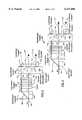
- FIG. 1illustrates in block diagram form the functionality of the optical router in accordance with the present invention
- FIG. 2 and FIG. 3illustrate in simplified schematic form a portion of a router in accordance with the present invention
- FIG. 4illustrates a spectral diagram of wavelength versus energy of a WDM signal
- FIG. 5illustrates a spectral diagram of an intermediate signal resulting from horizontally polarized input energy
- FIG. 6illustrates a spectral diagram of an intermediate optical signal resulting from vertically polarized input
- FIG. 7-FIG. 10illustrate spectral diagrams of various horizontal and vertically polarized intermediate signals after filtering in accordance with the present invention
- FIG. 11 and FIG. 12illustrate spectral diagrams of the spatially separated and routed output signals in accordance with the present invention
- FIG. 13illustrates in block diagram form a multi-stage programmable router in accordance with one embodiment of the present invention
- FIG. 14illustrates spectral diagrams of the pass band of each stage of the multi-stage filter shown in FIG. 13;
- FIG. 15illustrates in detail a portion of the wavelength filter of FIG. 2 and FIG. 3 in accordance with the present invention.
- FIG. 16A and FIG. 16Billustrates a computer simulated pass band of a flat top filter implementation in accordance with the present invention.
- FIG. 1illustrates in block diagram form the general funtionality of the present invention.
- a WDM signal 101comprising multiple channels each channel with its own range of wavelengths or frequencies.
- channelrefers to a particular range of frequencies or wavelengths that define a unique information signal.
- Each channelis ideally evenly spaced from adjacent channels, although this is not necessary. Uneven spacing may result in some inefficiency or complexity in design, but, as will be seen, the present invention can be adapted to such a channel system. This flexibility is important in that the channel placement is driven largely by the technical capabilities of transmitters (i.e., laser diodes) and detectors and so flexibility is of significant importance.
- each of the multiplexed input channelscan be selectively routed to any of the available output lines and all of the input channels can be placed on some line.
- the routerinclude at least the same number of outputs as the number of channels in the input signal, unless some of the output signals remain multiplexed as they leave the router.
- the present inventionis scaleable and so supports a greater number of output lines than the number of input channels in the multiplexed input signal. In such cases, some of the output lines will not carry any signal which increases routing flexibility but is a less efficient use of hardware.
- the WDM signalis fed as an input using conventional optical signal coupling techniques to 1 ⁇ 2 N router 1300.
- Router 1300receives N control signals C 1 -C N .
- Nis 3, however any number of control signals can be received by router 1300 due to the highly scaleable nature of the present invention.
- Router 1300generates 2 N unique output signals on output ports P 1 -P 2 N such as optical fibers or other suitable optical transmission means.
- Router 1300serves to spatially separate each channel in WDM signal 101. Each channel is programmably placed on one of the output ports as selected by the configuration bits C 1 -C N .
- configuration bits C 1 -C Nare conventional TTL compatible logic-level signals allowing easy integration with conventional electronic systems.
- the three output diagrams shown in FIG. 1are examples of channel locations output on each of the eight output ports of router 1300.
- the eight channels in WDM signal 101, as shown separately in FIG. 1will be referred to as channel 1-8 with channel 1 being the lowest wavelength and channel 8 being the highest wavelength grouping.
- With a (0,0,0) input on configuration bits C 1 -C Nthe lowest wavelength channel (i.e., channel 1) is coupled to output port P 1 .
- channel 1is presented to output port P 1 , channel 2 to output port P 2 , and channel 8 to output port P 2 N .
- configuration bitsare set to (0,0,1) channel 2 is coupled to output port P 1
- channel 1is coupled to output port P 2 and the remaining channels are coupled as shown in FIG. 1.
- configuration bitsare set to (1,0,0) channel 1 is coupled to port P 5
- channel 2 to port P 6channel 3 to port P 7 and channel 4 to port p 2 N and the remaining channels are coupled as shown in FIG. 1.
- channels 1-8are illustrated as evenly spaced, the channels may be unevenly spaced or one or more channels may be missing if transmitter/detectors are unavailable or the channel is not needed.
- the channelsmay also be more closely spaced. More or less channels may be provided.
- Current systemsare implemented with up to eight WDM channels in signal 101 and sixteen and sixty-four channel optical transceivers are available.
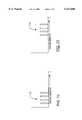
- FIG. 2 and FIG. 3illustrate a basic channel routing element 100 in schematic form in two control positions.
- each basic elementis under binary control from one of control bits C 1 -C N and hence, has two states.
- Each basic element 100serves to separate various portions of the frequency spectrum applied to an input port to select which of two output ports each of the separated signals are coupled to. As discussed later, these basic elements are cascaded to form the 1 ⁇ 2 N router 1300 in accordance with the present invention.
- each of the subsetsmay comprise more than one channel and may itself be a WDM signal although having a smaller bandwidth than the original WDM signal 101.
- Each of the linesare labeled as H indicating horizontal polarization, V indicating vertical polarization, or HV indicating mixed horizontal and vertical polarization in the optical signal at that point.
- WDM signal 101enters a birefringent element 102 that spatially separates horizontal and vertically polarized components of signal 101.
- Birefringent element 102comprises a material that allows the vertically polarized portion of the optical signal to pass through without changing course because they are ordinary waves in element 102.
- horizontally polarized wavesare redirected at an angle because of the birefringent walk-off effect. The angle of redirection is a well-known function of the particular materials chosen. Examples of materials suitable for construction of the birefringent elements used in the preferred embodiments include calcite, rutile, lithium niobate, YVO 4 based crystals, and the like.
- the horizontal componenttravels along path 103 as an extraordinary signal in birefringent element 102 while vertical component 104 travels as an ordinary signal and passes through without spatial reorientation.
- Signals 103 and 104both comprise the full spectrum of WDM signal 101.
- Both the horizontally and vertically polarized components 103 and 104are coupled to a programmable polarization rotator 106 under control of a control bit such as C 1 -C N shown in FIG. 1.
- Polarization rotator 106serves to selectively rotate the polarization state of each of signals 103 and 104 by a predefined amount. In the preferred embodiment, rotator 106 rotates the signals by either 0° (i.e., no rotation) or 90°.
- the polarization converter or rotator 106comprises one or more types of known elements including twisted nematic liquid crystal rotators, ferroelectric liquid crystal rotators, pi-cell based liquid crystal rotators, magneto-optic based Faraday rotators, acousto-optic and electro-optic based polarization rotators.
- Commercially available rotators having liquid crystal based technologyare preferred, although other rotator technologies may be applied to meet the needs of a particular application.
- the switching speed of these elementsranges from a few milliseconds to nanoseconds, therefore can be applied to a wide variety of systems to meet the needs of a particular application.
- FIG. 2illustrates the condition where the signals are rotated by 0° such that the signals exiting rotator 106 do not change polarization.
- FIG. 3illustrates the second case where polarization is rotated by 90° and the horizontally polarized component entering rotator 106 exits vertical polarization and the vertically polarized component exits with horizontal polarization. Again, at this stage, both the horizontal and vertical components comprise the entire spectrum of channels in WDM signal 101.
- Element 107comprises a plurality of birefringent waveplates (107a-107n in FIG. 15) at selected orientations.
- the combinationbecomes a polarization interference filter that serves to pass selected frequencies with horizontal polarization and a complimentary set of frequencies with vertical polarization.
- the polarization interference filterhas a comb filter response curve with substantially flat top or square wave spectral response.
- the polarization interference filteris sensitive to the polarization of the incoming optical signal.
- the spectral response to a horizontally polarized input signal when viewed at the same output point of birefringent element 108is complimentary to the spectral response of a vertically polarized input signal.
- Optical signals 105 and 115are coupled to birefringent element 108.
- Birefringent element 108has similar construction to birefringent element 102 and serves to spatially separate horizontally and vertically polarized components of the input optical signals 105 and 115.
- optical signal 115is broken into a vertical component 111 comprising the first set of channels and a horizontal component 112 comprising the second set of frequencies.
- optical signal 105is broken down into a vertical component 113 comprising the second set of frequencies and a horizontal component 114 comprising the first set of frequencies.
- birefringent element 108is selected such that the horizontal component 112 joins with the vertical component 113 and is output as optical signal 116 comprising the second set of frequencies.
- Optical signal 116includes both horizontal and vertical components.
- Optical combining means 109 and 110serve to combine the vertical component 111 with the horizontal component 114 to produce an output signal 117 comprising the first set of frequencies.
- Combining elements 109 and 110can take a variety of known forms including a retro-reflector, mirror, prism, or other optical signal combining means.
- Output signals 116 and 117must be physically aligned with an output port such as an optical fiber or a subsequent optical processing element.
- the vertical component 111comprises the second set of channels while the horizontal channel 112 comprises the first set of channels.
- the vertical component 113comprises the first set of channels and the horizontal component 114 comprises the second set of channels.
- Combining means 109 and 110operate in a manner similar to that described in FIG. 2 to provide a first output signal 116 comprising the first set of frequencies and a second output signal 117 comprising the second set of frequencies. In this manner, a single control signal applied to rotator 106 optically routes the subdivided WDM input signal.
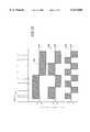
- FIG. 4illustrates eight channels making up WDM signal 101.
- wavelengthis illustrated on the horizontal axis while signal amplitude is illustrated on the vertical axis. While each channel is illustrated as a neatly separated square, it should be understood that in practice that the channels may comprise a range of frequencies having various amplitudes throughout the range of frequencies. The particular range of frequencies may be larger or smaller than shown in FIG. 4.
- FIG. 5the functionality of horizontally polarized input of the stacked birefringent waveplates 107 (shown in FIG. 2) is illustrated.
- the dashed line boxindicates the portion of the horizontally polarized input that is passed with vertical polarization.
- the portion of the signal outside of the dashed line boxis passed with horizontal (i.e., non-rotated) orientation.
- channels 1-4exit with vertical polarization if they enter stacked birefringent waveplates 107 with horizontal polarization.
- channels 5-8exit stacked birefringent waveplates 107 with horizontal polarization if they enter with horizontal polarization.
- FIG. 6illustrates a spectrum diagram when the input to stacked birefringent waveplates 107 has vertical polarization. This is shown in FIG. 2 by the lower signal and in FIG. 3 by the upper signal exiting rotator 106.
- the dashed lineindicates rotated wavelengths (i.e., wavelengths that will exit stacked birefringent waveplates 107 with horizontal polarization).
- channels 1-4are rotated and exit stacked birefringent waveplates 107 with horizontal polarization while channels 5-8 are not rotated and exit with their original vertical polarization.
- distinct sets of frequenciescan be distinguished although they still travel in the same optical paths 105 and 115 shown in FIG. 2 and FIG. 3.
- the construction of a filter to accomplish the function shown by the dotted line in FIG. 5 and FIG. 6will be described in greater detail hereinafter.
- FIG. 7-FIG. 10illustrate the various components as they are separated in birefringent element 108.
- FIG. 7shows the vertically polarized component 111 comprising channels 1-4. If the control signal applied to rotator 106 were inverted, signal 111 would comprise vertically polarized components of channels 5-8.
- component 112comprises horizontally polarized portions of channels 5-8 while if the control bit were inverted, signal 112 would comprise the horizontally polarized components of channels 1-4.
- FIG. 9illustrates signal 114 which comprises the horizontally polarized component of channels 1-4 while the inverse would be true if the control bit were inverted.
- signal component 113comprises the vertically polarized portions of channels 5-8 while if the configuration bit were inverted component 113 would comprise the vertically polarized components of channels 1-4.
- Signals 111 and 114are optically combined as illustrated in FIG. 2 to form output signal 117 comprising the horizontally and vertically polarized components of channels 1-4. If the control bit were inverted, output signal 117 would comprise the horizontally and vertically polarized components of channels 5-8. Conversely, components 112 and 113 are optically combined as the exit birefringent element 108 to form output signal 116 comprising the horizontally and vertically polarized components of channels 5-8. If the control bit were inverted, output signal 116 would comprise the horizontally and vertically polarized components of channels 1-4.
- One feature in accordance with the present inventionis that the routing is accomplished while conserving substantially all optical energy available in WDM signal 101. That is to say, regardless of the polarization of the signals in WDM signal 101 both the horizontal and vertically polarized components are used and recombined into output signal 116 and output signal 117 resulting in very low loss through router 1300 in accordance with the present invention.
- output signals 116 and 117comprise more than one channel and so themselves are WDM signals. Routing groups of channels may be useful in some circumstances, however, the preferred embodiment of the present invention uses multiple stage design to further decompose WDM signals 116 and 117 as shown in FIG. 11 and FIG. 12 into individual channel components that are spatially separated.
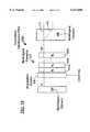
- FIG. 13illustrates in block diagram form router 1300 in accordance with the present invention.
- Router 1300is a three-stage router each stage accepting one control bit C 1 -C N .
- First stage 100comprises a single 1 ⁇ 2 router such as router 100 shown in FIG. 2 and FIG. 3.
- First stage 100is responsible for dividing WDM signal 101 into two groups.
- Second stage 200comprises two substantially identical routers that are similar to router 100 in stage 1.
- Routers 200also divide the WDM signals received on lines 116 and 117 into two output signals.
- Routers 200differ from router 100 in that the pass band of their polarization interference filter has narrower "tines" and more frequent tines.
- the pass band of stages 200is half the width of the pass band of stage 100 and has twice the frequency. This is accomplished by adding additional waveplates or increasing the retardation of the waveplates in the element 107 shown in FIG. 2 and FIG. 3.
- the third stagecomprises four router elements 300 that are similar in construction to router elements 200 and 100 discussed above.
- Each output from stage 200comprises two WDM channels.
- Each stage 300further divides the two WDM channels that are received into two single channel outputs on outputs P 1 -P 2 N .
- Each router element 300is coupled to a single configuration bit C 1 which selects the binary state.
- the cascaded design of binary router elements 100, 200, and 300 shown in FIG. 13allows three control bits to implement any of 2 N routing arrangements of the WDM signal 101 onto outputs P 1 -P 2 N .
- each of routing elements 100, 200, and 300could be individually controlled or programmed or some may receive no configuration bit and have a fixed demultiplexing function to meet the needs of a particular application.
- FIG. 14illustrates how the pass bands of router stages 100, 200, and 300 differ with respect to WDM signal 101 illustrated at the top of FIG. 14.
- a pass band of stage 100 indicated by the shaded portions in FIG. 14passes channels 1-4 if they enter with horizontal orientation without changing the orientation.
- Optical energy that enters with vertical polarization into stage 100will be passed without rotation if it was within channels 5-8. It is advantageous to have substantially flat pass band performance of each stage 100, 200, and 300 as shown in FIG. 14.
- stage 200 shown in FIG. 14it can be seen that channels 1-2 and 5-6 are passed if they enter with horizontal polarization while channels 3-4 and 7-8 are passed if they enter with vertical polarization.
- the channels that are not passedare rotated to have the opposite polarization as described hereinbefore.
- stage 300defines a pass band in which channels 1, 3, 5, and 7 are passed with horizontal polarization and channels 2, 4, 6, and 8 are passed with vertical polarization.
- FIG. 15illustrates in greater detail the construction of a flat top polarization interference filter controlled by polarization converter 106.
- Filter 205comprises N cascaded birefringent elements 107 sandwiched by polarization rotator 106 and birefringent elements 104 and 108.
- Conventional filter designcreates a shaped spectral response by sandwiching birefringent elements such as 107A-107N between two polarizers.
- the conventional designdoes not offer control which is provided by polarization converter.
- the conventional designalso wastes optical energy by filtering out all energy of a particular polarization at an output polarizer.
- the present inventionconserves this energy using birefringent elements 104 and 108 rather than a conventional polarizer.
- Each birefringent element 107A-107Nare oriented at a unique optic axis angle with respect to the optical axis of polarization converter 106.
- Any optical transmission functioncan be approximated by N terms of a Fourier series. From the coefficients of the approximating Fourier series the impulse response of the filter can be estimated.
- a filter of N elementsallows the approximation of the desired function by N+1 terms of a Fourier exponential series.
- An example of using five waveplates to synthesize the flat-top spectrumis shown in FIG. 16. By properly orienting the optical axis of the waveplates a relatively flat-top is achieved with a side-lobe compression ratio of 30 dB.
- FIG. 16A and FIG. 16Bthe flat top spectra are shown before and after the polarization converter 106 is switched.
- the vertical axisrepresents normalized transmission and the horizontal axis represents wavelength.
- the two spectraare complimentary to each other, which is one of the key factors in designing the wavelength router. It is because of this orthogonal characteristic that polarization rotator 106 can select either of the spectra and spatially separate them later using birefringent crystals. By increasing the sampling points or the number of waveplates a better transmission function that more closely approximates a flat top transmission with steep transitions is obtained.
- this transmission functioncan be a perfect square wave shape in the desired spectral bandwidth. Minimum side slopes, 100% transmission, and flat top response are possible. Practically, however, the physical size limits the number of stages a practical device will sacrifice some of the features such as ripple on the top, shallower slope, and side lobe fluctuation.
Landscapes
- Physics & Mathematics (AREA)
- General Physics & Mathematics (AREA)
- Optics & Photonics (AREA)
- Engineering & Computer Science (AREA)
- Computer Networks & Wireless Communication (AREA)
- Nonlinear Science (AREA)
- Signal Processing (AREA)
- Optical Communication System (AREA)
Abstract
Description
TABLE 1 ______________________________________ Control Spectral Control Spectral State Response State Response (C.sub.3,C.sub.2,C.sub.1) (P.sub.1 -P.sub.2.sup.N) (C.sub.3,C.sub.2,C.sub.1) (P.sub.1 -P.sub.2.sup.N) ______________________________________ (0,0,0) 1,2,3,4,5,6,7,8 (1,0,0) 5,6,7,8,1,2,3,4 (0,0,1) 2,1,4,3,6,5,8,7 (1,0,1) 6,5,8,7,2,1,4,3 (0,1,0) 3,4,1,2,7,8,5,6 (1,1,0) 8,7,5,6,3,4,1,2 (0,1,1) 4,3,2,1,8,7,6,5 (1,1,1) 7,8,6,5,4,3,2,1 ______________________________________
Claims (9)
Priority Applications (2)
| Application Number | Priority Date | Filing Date | Title |
|---|---|---|---|
| US09/411,935US6137606A (en) | 1996-10-29 | 1999-10-04 | Optical wavelength router |
| US09/659,524US6288807B1 (en) | 1996-10-29 | 2000-09-12 | Optical wavelength router |
Applications Claiming Priority (3)
| Application Number | Priority Date | Filing Date | Title |
|---|---|---|---|
| US08/739,424US5867291A (en) | 1996-10-29 | 1996-10-29 | Programmable wavelength router |
| US09/240,550US5978116A (en) | 1996-10-29 | 1999-01-29 | Programmable wavelength router |
| US09/411,935US6137606A (en) | 1996-10-29 | 1999-10-04 | Optical wavelength router |
Related Parent Applications (1)
| Application Number | Title | Priority Date | Filing Date |
|---|---|---|---|
| US09/240,550ContinuationUS5978116A (en) | 1996-10-29 | 1999-01-29 | Programmable wavelength router |
Related Child Applications (1)
| Application Number | Title | Priority Date | Filing Date |
|---|---|---|---|
| US09/659,524ContinuationUS6288807B1 (en) | 1996-10-29 | 2000-09-12 | Optical wavelength router |
Publications (1)
| Publication Number | Publication Date |
|---|---|
| US6137606Atrue US6137606A (en) | 2000-10-24 |
Family
ID=24972248
Family Applications (4)
| Application Number | Title | Priority Date | Filing Date |
|---|---|---|---|
| US08/739,424Expired - Fee RelatedUS5867291A (en) | 1996-07-23 | 1996-10-29 | Programmable wavelength router |
| US09/240,550Expired - Fee RelatedUS5978116A (en) | 1996-10-29 | 1999-01-29 | Programmable wavelength router |
| US09/411,935Expired - Fee RelatedUS6137606A (en) | 1996-10-29 | 1999-10-04 | Optical wavelength router |
| US09/659,524Expired - Fee RelatedUS6288807B1 (en) | 1996-10-29 | 2000-09-12 | Optical wavelength router |
Family Applications Before (2)
| Application Number | Title | Priority Date | Filing Date |
|---|---|---|---|
| US08/739,424Expired - Fee RelatedUS5867291A (en) | 1996-07-23 | 1996-10-29 | Programmable wavelength router |
| US09/240,550Expired - Fee RelatedUS5978116A (en) | 1996-10-29 | 1999-01-29 | Programmable wavelength router |
Family Applications After (1)
| Application Number | Title | Priority Date | Filing Date |
|---|---|---|---|
| US09/659,524Expired - Fee RelatedUS6288807B1 (en) | 1996-10-29 | 2000-09-12 | Optical wavelength router |
Country Status (7)
| Country | Link |
|---|---|
| US (4) | US5867291A (en) |
| EP (1) | EP0937346A4 (en) |
| JP (1) | JP2001503160A (en) |
| CN (1) | CN1235721A (en) |
| AU (1) | AU731680B2 (en) |
| CA (1) | CA2268131A1 (en) |
| WO (1) | WO1998019415A1 (en) |
Cited By (20)
| Publication number | Priority date | Publication date | Assignee | Title |
|---|---|---|---|---|
| US6288807B1 (en)* | 1996-10-29 | 2001-09-11 | Chorum Technologies Lp | Optical wavelength router |
| US6353467B1 (en) | 1998-01-06 | 2002-03-05 | Chorum Technologies Inc. | Acute twist nematic (ATN) liquid crystal device for optical communication applications |
| US6396609B1 (en) | 1999-12-20 | 2002-05-28 | Chorum Technologies, Lp | Dispersion compensation for optical systems |
| WO2002046815A1 (en)* | 2000-12-07 | 2002-06-13 | Alcatel | Device for frequency band demultiplexing |
| US6455841B2 (en)* | 2000-03-02 | 2002-09-24 | Chorum Technologies Lp | Optical wavelength router based on polarization interferometer |
| US6519060B1 (en)* | 1999-06-04 | 2003-02-11 | Chorum Technologies Lp | Synchronous optical network in frequency domain |
| US20030058497A1 (en)* | 2001-09-27 | 2003-03-27 | Nortel Networks Limited | All-optical switching sites for an agile optical network |
| US6552833B2 (en) | 1997-04-15 | 2003-04-22 | Macro-Vision Communications, Inc. | Programmable optical add/drop multiplexer |
| US6559992B2 (en) | 2000-03-27 | 2003-05-06 | Chorum Technologies Lp | Adjustable chromatic dispersion compensation |
| US20030113055A1 (en)* | 2001-12-18 | 2003-06-19 | Jing Zhao | Solid-state optical wavelength switches |
| US6594049B1 (en)* | 1999-10-29 | 2003-07-15 | Lucent Technologies Inc. | Optical router |
| US6600582B1 (en) | 1997-03-24 | 2003-07-29 | Chorum Technologies Lp | Optical add/drop wavelength switch |
| US6614573B1 (en) | 2001-01-30 | 2003-09-02 | Avanex Corporation | Switchable interleaved channel separator devices and systems |
| US6680470B1 (en) | 2001-11-14 | 2004-01-20 | Dicon Fiberoptics, Inc. | Interleaver with thermal and chromatic dispersion compensation |
| US6766074B1 (en) | 2001-08-15 | 2004-07-20 | Corning Incorporated | Demultiplexer/multiplexer with a controlled variable path length device |
| US6791753B1 (en) | 2002-03-18 | 2004-09-14 | Alliance Fiber Optic Products, Inc. | Retro-reflective fiber optic interleaver |
| US20040247312A1 (en)* | 2001-12-03 | 2004-12-09 | Fujitsu Limited | Optical communication system |
| US20050111785A1 (en)* | 2003-10-09 | 2005-05-26 | Jing Zhao | Multi-port optical switches |
| US20090097251A1 (en)* | 2007-10-04 | 2009-04-16 | Samsung Electro-Mechanics Co., Ltd. | Light homogenizing device and display apparatus including the same |
| US10439302B2 (en) | 2017-06-08 | 2019-10-08 | Pct International, Inc. | Connecting device for connecting and grounding coaxial cable connectors |
Families Citing this family (114)
| Publication number | Priority date | Publication date | Assignee | Title |
|---|---|---|---|---|
| US5978125A (en)* | 1995-11-30 | 1999-11-02 | Yao; X. Steve | Compact programmable photonic variable delay devices |
| US6005697A (en)* | 1996-07-23 | 1999-12-21 | Macro-Vision Communications, L.L.C. | Multi-wavelength cross-connect optical network |
| US6847786B2 (en) | 1996-10-29 | 2005-01-25 | Ec-Optics Technology, Inc. | Compact wavelength filter using optical birefringence and reflective elements |
| US6208444B1 (en)* | 1996-10-29 | 2001-03-27 | Chorum Technologies Inc. | Apparatus for wavelength demultiplexing using a multi-cavity etalon |
| US6163393A (en)* | 1996-10-29 | 2000-12-19 | Chorum Technologies Inc. | Method and apparatus for wavelength multipexing/demultiplexing |
| US6545783B1 (en) | 1996-10-29 | 2003-04-08 | Chorum Technologies Lp | Optical wavelength add/drop multiplexer |
| US6498680B1 (en) | 1996-10-29 | 2002-12-24 | Chorum Technologies Lp | Compact tunable optical wavelength interleaver |
| US6115155A (en) | 1996-10-29 | 2000-09-05 | Chorum Technologies Inc. | System for dealing with faults in an optical link |
| US6208442B1 (en) | 1998-03-26 | 2001-03-27 | Chorum Technologies, Inc. | Programmable optical multiplexer |
| US6049404A (en)* | 1997-04-02 | 2000-04-11 | Macro-Vision Communications Inc. | N+M digitally programmable optical routing switch |
| US6519022B1 (en)* | 1997-04-02 | 2003-02-11 | Chorum Technologies Lp | Optical routing switch using symmetric liquid crystal cells |
| JP3737628B2 (en)* | 1998-03-20 | 2006-01-18 | 富士通株式会社 | Gain equalizer and optical amplifier |
| JP3567763B2 (en)* | 1998-06-12 | 2004-09-22 | Kddi株式会社 | Optical transmitter |
| US6519064B1 (en)* | 1998-06-19 | 2003-02-11 | Lucent Technologies Inc. | Scalable add/drop architecture for lightwave communication system |
| US6370286B1 (en) | 1998-08-21 | 2002-04-09 | Corning Incorporated | Tunable periodic filter |
| US6134358A (en) | 1998-08-27 | 2000-10-17 | Chorum Technologies Inc. | N x N switch array with reduced components |
| US6721508B1 (en) | 1998-12-14 | 2004-04-13 | Tellabs Operations Inc. | Optical line terminal arrangement, apparatus and methods |
| US6160665A (en)* | 1999-06-04 | 2000-12-12 | Chorum Technologies Inc. | High extinction ratio polarization beamsplitter |
| US6275322B1 (en) | 1999-06-08 | 2001-08-14 | Jds Uniphase Corporation | Michelson phase shifter interleaver/deinterleavers |
| US6341040B1 (en) | 1999-06-08 | 2002-01-22 | Jds Uniphase Corporation | Multi-plate comb filter and applications therefor |
| US6154585A (en)* | 1999-06-17 | 2000-11-28 | Jds Fitel Inc. | 11/2×2 optical switch |
| US6285500B1 (en) | 1999-06-29 | 2001-09-04 | Corning Incorporated | Wavelength selective switch |
| US7194161B1 (en) | 1999-06-30 | 2007-03-20 | The Regents Of The University Of California | Wavelength-conserving grating router for intermediate wavelength density |
| WO2001013079A1 (en)* | 1999-08-18 | 2001-02-22 | Swinburne University | Method and apparatus for the resolution of beams of electromagnetic radiation |
| US6735016B1 (en) | 1999-09-15 | 2004-05-11 | Spectraswitch, Inc. | Electro-optically controllable polarization insensitive optical device |
| US6594063B1 (en) | 1999-09-15 | 2003-07-15 | Spectraswitch, Inc. | Birefringent optical device |
| US6236506B1 (en)* | 1999-09-23 | 2001-05-22 | Avanex Corporation | Reflection-type optical circulation utilizing a lens and birefringent plates |
| US6853488B1 (en) | 1999-09-23 | 2005-02-08 | Avanex Corporation | Reflection-type optical circulator utilizing a lens and birefringent plates |
| US6560015B1 (en)* | 1999-09-23 | 2003-05-06 | Avanex Corporation | High-isolation dense wavelength division multiplexer utilizing birefringent plates and a non-linear interferometer |
| EP1163751B1 (en)* | 1999-10-01 | 2011-03-30 | Finisar Corporation | Otpical mux/demux |
| US6373604B1 (en)* | 1999-10-01 | 2002-04-16 | New Focus, Inc. | Optical MUX/DEMUX |
| WO2001031818A1 (en)* | 1999-10-28 | 2001-05-03 | Fujitsu Limited | Transmission system |
| US6301046B1 (en) | 1999-12-31 | 2001-10-09 | Jds Uniphase Corporation | Interleaver/deinterleavers causing little or no dispersion of optical signals |
| US6335830B1 (en) | 1999-12-31 | 2002-01-01 | Jds Uniphase Corporation | Double-pass folded interleaver/deinterleavers |
| US6342968B1 (en) | 1999-12-31 | 2002-01-29 | Jds Uniphase Corporation | Frequency tuning of optical devices |
| US6337770B1 (en)* | 1999-12-31 | 2002-01-08 | Jds Uniphase Corporation | Single-pass folded interleaver/deinterleavers |
| GB2363675B (en)* | 2000-01-19 | 2004-05-26 | Advantest Corp | Wideband optical amplifier and wideband variable wavelength optical source |
| US6687462B1 (en) | 2000-02-01 | 2004-02-03 | Oplink Communications, Inc. | Wavelength slicer for optical signal switching |
| US6498872B2 (en)* | 2000-02-17 | 2002-12-24 | Jds Uniphase Inc. | Optical configuration for a dynamic gain equalizer and a configurable add/drop multiplexer |
| GB2359434B (en)* | 2000-02-18 | 2002-09-11 | Marconi Comm Ltd | Optical communication system |
| EP1126650A3 (en)* | 2000-02-18 | 2007-01-03 | Ericsson AB | Optical communication system |
| US6463189B1 (en) | 2000-02-24 | 2002-10-08 | Avanex Corporation | Method and apparatus for optical switching devices utilizing a bi-morphic piezoelectric apparatus |
| US6421177B1 (en) | 2000-03-03 | 2002-07-16 | Arroyo Optics, Inc. | Interleaving optical filter |
| US6333816B1 (en) | 2000-03-03 | 2001-12-25 | Jds Uniphase Corporation | Apparatus capable of operating as interleaver/deinterleavers or filters |
| US6252711B1 (en)* | 2000-03-21 | 2001-06-26 | Lucent Technologies, Inc | Polarization diversity for birefingent filters |
| US6441960B1 (en)* | 2000-04-20 | 2002-08-27 | Oplink Communications, Inc. | Optical interleavers with minimized dispersion |
| US6310715B1 (en)* | 2000-04-26 | 2001-10-30 | The United States Of America As Represented By The United States Air Force | Crystal stack for coherent optical beam combination |
| US6426816B1 (en)* | 2000-05-01 | 2002-07-30 | Chorum Technologies, Lp | Wide transmission optical comb filter with wide pass band and wide stop band |
| WO2001091342A2 (en)* | 2000-05-24 | 2001-11-29 | Purdue Research Foundation | Method and system for polarization control and polarization mode dispersion compensation for wideband optical signals |
| US6781754B2 (en) | 2000-06-07 | 2004-08-24 | Cirvine Corporation | Interleaver using spatial birefringent elements |
| US6693743B2 (en) | 2000-06-07 | 2004-02-17 | Cirvine Corporation | Birefringent devices |
| US6687054B2 (en) | 2000-06-07 | 2004-02-03 | Cirvine Corporation | Apparatus and method for low dispersion in communications |
| US6731430B2 (en) | 2000-06-07 | 2004-05-04 | Cirvine Corporation | Low crosstalk flat band filter |
| US6452546B1 (en)* | 2000-06-14 | 2002-09-17 | Hrl Laboratories, Llc | Wavelength division multiplexing methods and apparatus for constructing photonic beamforming networks |
| US6628449B2 (en) | 2000-11-01 | 2003-09-30 | Cirvine Corporation | Tandem comb filter |
| WO2002001773A2 (en)* | 2000-06-23 | 2002-01-03 | Cirvine Corporation | Channel multiplexer and demultiplexer for optical communications |
| US6563641B2 (en) | 2000-06-23 | 2003-05-13 | Cirvine Corporation | Fold interleaver |
| WO2002027370A1 (en)* | 2000-06-30 | 2002-04-04 | Nortel Networks (Photonics) Pty Ltd | Optical filter for frequency dependent filtering |
| CA2354361A1 (en)* | 2000-08-01 | 2002-02-01 | Jds Uniphase Inc. | Virtual waveplate and optical channel interleaver formed therewith |
| US6396629B1 (en)* | 2000-08-24 | 2002-05-28 | Avanex Corporation | Multi-functional optical device utilizing multiple birefringent plates and a non-linear interferometer |
| US6459487B1 (en) | 2000-09-05 | 2002-10-01 | Gang Paul Chen | System and method for fabricating components of precise optical path length |
| WO2002021195A2 (en) | 2000-09-07 | 2002-03-14 | Terra-Op Ltd. | Method and system for ultra-fast switching of optical signals |
| US6466704B1 (en) | 2000-09-13 | 2002-10-15 | Nortel Networks (Photonics) Pty Ltd. | Optical filtering method and device |
| US6687428B2 (en) | 2000-09-21 | 2004-02-03 | Tera Op (Usa) Inc. | Optical switch |
| US6459827B1 (en) | 2000-10-02 | 2002-10-01 | John N. Hait | Polarization-stabilizing, phase-and-polarization-insensitive, photonic data router |
| US6477287B1 (en) | 2000-10-02 | 2002-11-05 | John N. Hait | Polarization-preserving, phase-and-polarization-insensitive, photonic data router |
| US6427033B1 (en) | 2000-10-02 | 2002-07-30 | John N. Hait | Photonic image router |
| US6704143B1 (en) | 2000-10-23 | 2004-03-09 | Adc Telecommunications, Inc. | Method and apparatus for adjusting an optical element to achieve a precise length |
| WO2002039176A1 (en)* | 2000-11-10 | 2002-05-16 | Sumitomo Electric Industries, Ltd. | Interleaver, filter included therein, and interleaver system |
| US6762876B2 (en)* | 2000-11-20 | 2004-07-13 | Terraop Ltd. | Optical converter with a designated output wavelength |
| US6535335B2 (en) | 2000-11-22 | 2003-03-18 | Optellios, Inc. | Optical polarization encoder |
| US7127179B2 (en)* | 2000-11-22 | 2006-10-24 | Optellios, Inc. | Polarization encoder device |
| US6429962B1 (en)* | 2000-12-05 | 2002-08-06 | Chorum Technologies Lp | Dynamic gain equalizer for optical amplifiers |
| US7031060B2 (en) | 2001-01-19 | 2006-04-18 | Jds Uniphase Corporation | Non-moving parts add/drop device |
| US6907167B2 (en) | 2001-01-19 | 2005-06-14 | Gazillion Bits, Inc. | Optical interleaving with enhanced spectral response and reduced polarization sensitivity |
| US20020131142A1 (en)* | 2001-01-31 | 2002-09-19 | Chi-Hao Cheng | System and method for tailoring dispersion within an optical communication system |
| US6694066B2 (en) | 2001-02-14 | 2004-02-17 | Finisar Corporation | Method and apparatus for an optical filter |
| US6684002B2 (en) | 2001-02-14 | 2004-01-27 | Finisar Corporation | Method and apparatus for an optical filter |
| US7006279B2 (en)* | 2001-02-16 | 2006-02-28 | Ec-Optics Technology Inc. | Optical harmonic equalization control systems and methods |
| US6885821B2 (en)* | 2001-02-27 | 2005-04-26 | Avanex Corporation | Full-duplex optical add/drop communications system utilizing central light sources |
| US6690846B2 (en)* | 2001-03-01 | 2004-02-10 | Chorum Technologies Lp | Dispersion-compensated optical wavelength router |
| US20020131125A1 (en)* | 2001-03-16 | 2002-09-19 | Myers Michael H. | Replicated-spectrum photonic transceiving |
| US6407846B1 (en) | 2001-03-16 | 2002-06-18 | All Optical Networks, Inc. | Photonic wavelength shifting method |
| US20020131100A1 (en)* | 2001-03-16 | 2002-09-19 | Myers Michael H. | Method for photonic wavelength error detection |
| US6809863B2 (en) | 2001-06-07 | 2004-10-26 | Cirvine Corporation | Low dispersion filters |
| US20020191913A1 (en)* | 2001-06-08 | 2002-12-19 | Honeywell International Inc. | Apparatus and method for processing light |
| US7106508B2 (en)* | 2001-06-11 | 2006-09-12 | Finisar Corporation | Hybrid cell |
| US6529326B2 (en) | 2001-06-13 | 2003-03-04 | Jds Uniphase Corporation | Tunable optical filter |
| JP4697917B2 (en)* | 2001-06-18 | 2011-06-08 | 大日本印刷株式会社 | IC card whose operating system can be switched by an optical sensor and IC card reader / writer |
| US6639707B2 (en) | 2001-06-25 | 2003-10-28 | Cirvine Corporation | Tandem interleaver |
| US6900938B2 (en) | 2001-06-25 | 2005-05-31 | Bin Zhao | Low dispersion interleaver |
| US7154668B2 (en) | 2001-07-10 | 2006-12-26 | Optellios, Inc. | Wavelength dependent optical attenuator and variable attenuation profile controller |
| JP2003035892A (en)* | 2001-07-25 | 2003-02-07 | Fdk Corp | Optical shutter |
| US6515786B1 (en) | 2001-08-03 | 2003-02-04 | Chorum Technologies Lp | Bandwidth variable wavelength router and method of operation |
| GB2378594A (en)* | 2001-08-10 | 2003-02-12 | Marconi Caswell Ltd | Polarisation splitting wavelength router |
| WO2003017537A1 (en)* | 2001-08-16 | 2003-02-27 | Telefonaktiebolaget Lm Ericsson (Publ) | Optical amplifier |
| US6717719B1 (en)* | 2001-10-01 | 2004-04-06 | The United States Of America As Represented By The Secretary Of The Air Force | Coherent optical beam combination using double-coated glass mirrors/mirror pairs |
| US20030076568A1 (en)* | 2001-10-22 | 2003-04-24 | Adc Telecommunications, Inc. | Light frequency stabilizer |
| US6798951B2 (en)* | 2001-11-12 | 2004-09-28 | Pts Corporation | Wavelength router with a transmissive dispersive element |
| US6665463B2 (en) | 2002-04-02 | 2003-12-16 | Tera Op, Inc. | Optical switching system |
| US7154659B1 (en)* | 2002-04-18 | 2006-12-26 | General Photonics Corporation | Optical depolarizers and DGD generators based on optical delay |
| US6850364B2 (en) | 2002-06-12 | 2005-02-01 | Finisar Corporation | Method and apparatus for an optical multiplexer and demultiplexer with an optical processing loop |
| US7268944B2 (en)* | 2002-06-12 | 2007-09-11 | Finisar Corporation | Optical interleaver, filter cell, and component design with reduced chromatic dispersion |
| US20040223222A1 (en)* | 2002-06-12 | 2004-11-11 | Schott Daniel Philip | Hermetically sealed collimator and optical interleaver design |
| US7173763B2 (en)* | 2002-06-12 | 2007-02-06 | Finisar Corporation | Optical interleaver and filter cell design with enhanced clear aperture |
| US20040227996A1 (en)* | 2002-06-12 | 2004-11-18 | Tengda Du | Optical interleaver and filter cell design with enhanced thermal stability |
| US7057716B2 (en)* | 2003-10-28 | 2006-06-06 | Hrl Laboratories, Llc | White cell antenna beamformers |
| US9530132B2 (en)* | 2004-01-27 | 2016-12-27 | George Chester Cox | System and method for customer video authentication to prevent identity theft |
| US7218451B2 (en)* | 2004-02-05 | 2007-05-15 | Oplink Communications, Inc. | Integrated optical multiplexer and demultiplexer |
| US7723670B1 (en) | 2007-03-26 | 2010-05-25 | General Photonics Corporation | Optical differential group delay module with folded optical path |
| CN102045127B (en)* | 2009-10-23 | 2014-12-10 | 华为技术有限公司 | Receiving device, sending device, system and method for photolytic polarization multiplexing |
| JP5459020B2 (en)* | 2010-03-31 | 2014-04-02 | 富士通オプティカルコンポーネンツ株式会社 | Optical receiver and communication system |
| JP7589259B2 (en)* | 2020-12-29 | 2024-11-25 | モノクロム エス.エル. | Spectral splitting device |
| CN118033809A (en)* | 2022-11-14 | 2024-05-14 | 武汉光迅科技股份有限公司 | Splicing filter, splicing method and electronic equipment |
Citations (12)
| Publication number | Priority date | Publication date | Assignee | Title |
|---|---|---|---|---|
| US4919522A (en)* | 1988-02-25 | 1990-04-24 | Geo-Centers, Inc. | Optical switch having birefringent element |
| US5136671A (en)* | 1991-08-21 | 1992-08-04 | At&T Bell Laboratories | Optical switch, multiplexer, and demultiplexer |
| US5363228A (en)* | 1993-03-05 | 1994-11-08 | General Electric Company | Optical device with spatial light modulators for switching arbitrarily polarized light |
| US5381250A (en)* | 1992-11-06 | 1995-01-10 | Displaytech, Inc. | Electro-optical switch with 4 port modules with electro-optic polarization rotators |
| US5414541A (en)* | 1993-06-01 | 1995-05-09 | Bell Communications Research, Inc. | Optical switch employing first and second ferroelectric cells with alignment layers having alignment directions offset by 45° |
| US5488500A (en)* | 1994-08-31 | 1996-01-30 | At&T Corp. | Tunable add drop optical filtering method and apparatus |
| US5596661A (en)* | 1994-12-28 | 1997-01-21 | Lucent Technologies Inc. | Monolithic optical waveguide filters based on Fourier expansion |
| US5606439A (en)* | 1996-04-10 | 1997-02-25 | Macro-Vision Technology , Inc. | Tunable add/drop optical filter |
| US5680490A (en)* | 1995-09-08 | 1997-10-21 | Lucent Technologies Inc. | Comb splitting system and method for a multichannel optical fiber communication network |
| US5694233A (en)* | 1996-07-23 | 1997-12-02 | Macro-Vision Communications, Llc | Switchable wavelength router |
| US5809190A (en)* | 1996-11-13 | 1998-09-15 | Applied Fiber Optics, Inc. | Apparatus and method of making a fused dense wavelength-division multiplexer |
| US5978116A (en)* | 1996-10-29 | 1999-11-02 | Chorum Technologies Inc. | Programmable wavelength router |
Family Cites Families (9)
| Publication number | Priority date | Publication date | Assignee | Title |
|---|---|---|---|---|
| US3503670A (en)* | 1967-01-16 | 1970-03-31 | Ibm | Multifrequency light processor and digital deflector |
| US4461543A (en)* | 1982-03-26 | 1984-07-24 | Sperry Corporation | Electro optic switch |
| US4566761A (en) | 1984-09-13 | 1986-01-28 | Gte Laboratories Incorporated | Birefringent optical wavelength multiplexer/demultiplexer |
| US4685773A (en)* | 1984-09-13 | 1987-08-11 | Gte Laboratories Incorporated | Birefringent optical multiplexer with flattened bandpass |
| WO1989002614A1 (en)* | 1987-09-11 | 1989-03-23 | British Telecommunications Public Limited Company | An optical space switch |
| US4987567A (en)* | 1988-11-21 | 1991-01-22 | Gte Laboratories Incorporated | Optical wavelength multiplexer/demultiplexer and demultiplexer/remultiplexer |
| US5912748A (en)* | 1996-07-23 | 1999-06-15 | Chorum Technologies Inc. | Switchable wavelength router |
| US6097518A (en)* | 1996-10-29 | 2000-08-01 | Chorum Technologies Inc. | N x M optical wavelength routing switch |
| US6005518A (en)* | 1997-12-31 | 1999-12-21 | Kallina; Henry D. | Coaxial cable RF leakage detector |
- 1996
- 1996-10-29USUS08/739,424patent/US5867291A/ennot_activeExpired - Fee Related
- 1997
- 1997-10-15JPJP10520505Apatent/JP2001503160A/ennot_activeCeased
- 1997-10-15CACA002268131Apatent/CA2268131A1/ennot_activeAbandoned
- 1997-10-15CNCN97199305Apatent/CN1235721A/enactivePending
- 1997-10-15WOPCT/US1997/018417patent/WO1998019415A1/ennot_activeApplication Discontinuation
- 1997-10-15AUAU46743/97Apatent/AU731680B2/ennot_activeCeased
- 1997-10-15EPEP97945575Apatent/EP0937346A4/ennot_activeWithdrawn
- 1999
- 1999-01-29USUS09/240,550patent/US5978116A/ennot_activeExpired - Fee Related
- 1999-10-04USUS09/411,935patent/US6137606A/ennot_activeExpired - Fee Related
- 2000
- 2000-09-12USUS09/659,524patent/US6288807B1/ennot_activeExpired - Fee Related
Patent Citations (12)
| Publication number | Priority date | Publication date | Assignee | Title |
|---|---|---|---|---|
| US4919522A (en)* | 1988-02-25 | 1990-04-24 | Geo-Centers, Inc. | Optical switch having birefringent element |
| US5136671A (en)* | 1991-08-21 | 1992-08-04 | At&T Bell Laboratories | Optical switch, multiplexer, and demultiplexer |
| US5381250A (en)* | 1992-11-06 | 1995-01-10 | Displaytech, Inc. | Electro-optical switch with 4 port modules with electro-optic polarization rotators |
| US5363228A (en)* | 1993-03-05 | 1994-11-08 | General Electric Company | Optical device with spatial light modulators for switching arbitrarily polarized light |
| US5414541A (en)* | 1993-06-01 | 1995-05-09 | Bell Communications Research, Inc. | Optical switch employing first and second ferroelectric cells with alignment layers having alignment directions offset by 45° |
| US5488500A (en)* | 1994-08-31 | 1996-01-30 | At&T Corp. | Tunable add drop optical filtering method and apparatus |
| US5596661A (en)* | 1994-12-28 | 1997-01-21 | Lucent Technologies Inc. | Monolithic optical waveguide filters based on Fourier expansion |
| US5680490A (en)* | 1995-09-08 | 1997-10-21 | Lucent Technologies Inc. | Comb splitting system and method for a multichannel optical fiber communication network |
| US5606439A (en)* | 1996-04-10 | 1997-02-25 | Macro-Vision Technology , Inc. | Tunable add/drop optical filter |
| US5694233A (en)* | 1996-07-23 | 1997-12-02 | Macro-Vision Communications, Llc | Switchable wavelength router |
| US5978116A (en)* | 1996-10-29 | 1999-11-02 | Chorum Technologies Inc. | Programmable wavelength router |
| US5809190A (en)* | 1996-11-13 | 1998-09-15 | Applied Fiber Optics, Inc. | Apparatus and method of making a fused dense wavelength-division multiplexer |
Non-Patent Citations (16)
| Title |
|---|
| Ammann, "Synthesis of Electro-Optic Shutters havin g a Prescribed Transmission vs Voltage Characteristics", Journal of the Optical Society of America (vol. 56, No. 8, pp. 1081-1088, Aug. 1996). |
| Ammann, Synthesis of Electro Optic Shutters havin g a Prescribed Transmission vs Voltage Characteristics , Journal of the Optical Society of America (vol. 56, No. 8, pp. 1081 1088, Aug. 1996).* |
| Chung et al., "Analysis of a Tunable Multichannel Two-Mode-Interference Wavelength Division Mutliplexer/Demultiplexer", Journal of Lightwave Technology (vol. 7, No. 5, May 1989). |
| Chung et al., Analysis of a Tunable Multichannel Two Mode Interference Wavelength Division Mutliplexer/Demultiplexer , Journal of Lightwave Technology (vol. 7, No. 5, May 1989).* |
| Damask et al., "Wavelength-Division Multiplexing using Channel-Dropping Filters", Journal of Lightwave Technology (vol. 11, No. 3, Mar. 1993). |
| Damask et al., Wavelength Division Multiplexing using Channel Dropping Filters , Journal of Lightwave Technology (vol. 11, No. 3, Mar. 1993).* |
| Dingel and Izutsu, "Multifunction Optical Filter with a Michelson-Gires-Tournois Interferometer for Wavelength-Division-Multiplexed Network System Applications", Optical Letters (vol. 23, p. 1099, Jul. 1998). |
| Dingel and Izutsu, Multifunction Optical Filter with a Michelson Gires Tournois Interferometer for Wavelength Division Multiplexed Network System Applications , Optical Letters (vol. 23, p. 1099, Jul. 1998).* |
| Harris et al., "Optical Network Synthesis Using Birefringent Crystals. *I. Synthesis of Lossless Networks of Equal-Length Crystals", Journal of the Optical Society of America (vol. 54, No. 10, pp. 1267-1279, Oct. 1964). |
| Harris et al., Optical Network Synthesis Using Birefringent Crystals. *I. Synthesis of Lossless Networks of Equal Length Crystals , Journal of the Optical Society of America (vol. 54, No. 10, pp. 1267 1279, Oct. 1964).* |
| Inoue et al., "A Four-Channel Optical Waveguide Multi/Demultiplexer foe 5-GHz Spaced Optical FDM Transmission", Journal of Lightwave Technology (vol. 6, No. 2, Feb. 1988). |
| Inoue et al., A Four Channel Optical Waveguide Multi/Demultiplexer foe 5 GHz Spaced Optical FDM Transmission , Journal of Lightwave Technology (vol. 6, No. 2, Feb. 1988).* |
| Nosu et al., "Optical FDM Transmission Technique", Journal of Lightwave Technology (vol. LT-5, No. 9, Sep. 1987). |
| Nosu et al., Optical FDM Transmission Technique , Journal of Lightwave Technology (vol. LT 5, No. 9, Sep. 1987).* |
| Senior et al., "Devices for Wavelength-Multiplexing and Demultiplexing", IEE Proceedings (vol. 136, Pt. J, No. 3, Jun. 1989). |
| Senior et al., Devices for Wavelength Multiplexing and Demultiplexing , IEE Proceedings (vol. 136, Pt. J, No. 3, Jun. 1989).* |
Cited By (26)
| Publication number | Priority date | Publication date | Assignee | Title |
|---|---|---|---|---|
| US6288807B1 (en)* | 1996-10-29 | 2001-09-11 | Chorum Technologies Lp | Optical wavelength router |
| US6600582B1 (en) | 1997-03-24 | 2003-07-29 | Chorum Technologies Lp | Optical add/drop wavelength switch |
| US6552833B2 (en) | 1997-04-15 | 2003-04-22 | Macro-Vision Communications, Inc. | Programmable optical add/drop multiplexer |
| US6353467B1 (en) | 1998-01-06 | 2002-03-05 | Chorum Technologies Inc. | Acute twist nematic (ATN) liquid crystal device for optical communication applications |
| US6519060B1 (en)* | 1999-06-04 | 2003-02-11 | Chorum Technologies Lp | Synchronous optical network in frequency domain |
| US6594049B1 (en)* | 1999-10-29 | 2003-07-15 | Lucent Technologies Inc. | Optical router |
| US6396609B1 (en) | 1999-12-20 | 2002-05-28 | Chorum Technologies, Lp | Dispersion compensation for optical systems |
| US6455841B2 (en)* | 2000-03-02 | 2002-09-24 | Chorum Technologies Lp | Optical wavelength router based on polarization interferometer |
| US6559992B2 (en) | 2000-03-27 | 2003-05-06 | Chorum Technologies Lp | Adjustable chromatic dispersion compensation |
| US20030002102A1 (en)* | 2000-12-07 | 2003-01-02 | Sabry Khalfallah | Device for frequency band demultiplexing |
| FR2818059A1 (en)* | 2000-12-07 | 2002-06-14 | Cit Alcatel | DEVICE FOR DEMULTIPLEXING FREQUENCY BANDS |
| WO2002046815A1 (en)* | 2000-12-07 | 2002-06-13 | Alcatel | Device for frequency band demultiplexing |
| US6614573B1 (en) | 2001-01-30 | 2003-09-02 | Avanex Corporation | Switchable interleaved channel separator devices and systems |
| US6721078B1 (en) | 2001-01-30 | 2004-04-13 | Avanex Corporation | Switchable interleaved channel separator devices and systems |
| US6766074B1 (en) | 2001-08-15 | 2004-07-20 | Corning Incorporated | Demultiplexer/multiplexer with a controlled variable path length device |
| US20030058497A1 (en)* | 2001-09-27 | 2003-03-27 | Nortel Networks Limited | All-optical switching sites for an agile optical network |
| US6680470B1 (en) | 2001-11-14 | 2004-01-20 | Dicon Fiberoptics, Inc. | Interleaver with thermal and chromatic dispersion compensation |
| US20040247312A1 (en)* | 2001-12-03 | 2004-12-09 | Fujitsu Limited | Optical communication system |
| US6718082B2 (en) | 2001-12-18 | 2004-04-06 | Agiltron, Inc. | Solid-State optical wavelength switches |
| US20030113055A1 (en)* | 2001-12-18 | 2003-06-19 | Jing Zhao | Solid-state optical wavelength switches |
| US6791753B1 (en) | 2002-03-18 | 2004-09-14 | Alliance Fiber Optic Products, Inc. | Retro-reflective fiber optic interleaver |
| US20050111785A1 (en)* | 2003-10-09 | 2005-05-26 | Jing Zhao | Multi-port optical switches |
| US7224860B2 (en) | 2003-10-09 | 2007-05-29 | Jing Zhao | Multi-port optical switches |
| US20090097251A1 (en)* | 2007-10-04 | 2009-04-16 | Samsung Electro-Mechanics Co., Ltd. | Light homogenizing device and display apparatus including the same |
| US10439302B2 (en) | 2017-06-08 | 2019-10-08 | Pct International, Inc. | Connecting device for connecting and grounding coaxial cable connectors |
| US10855003B2 (en) | 2017-06-08 | 2020-12-01 | Pct International, Inc. | Connecting device for connecting and grounding coaxial cable connectors |
Also Published As
| Publication number | Publication date |
|---|---|
| US6288807B1 (en) | 2001-09-11 |
| US5978116A (en) | 1999-11-02 |
| EP0937346A4 (en) | 1999-10-27 |
| CA2268131A1 (en) | 1998-05-07 |
| JP2001503160A (en) | 2001-03-06 |
| AU4674397A (en) | 1998-05-22 |
| CN1235721A (en) | 1999-11-17 |
| US5867291A (en) | 1999-02-02 |
| EP0937346A1 (en) | 1999-08-25 |
| WO1998019415A1 (en) | 1998-05-07 |
| AU731680B2 (en) | 2001-04-05 |
Similar Documents
| Publication | Publication Date | Title |
|---|---|---|
| US6137606A (en) | Optical wavelength router | |
| AU727466B2 (en) | Switchable wavelength router | |
| US5912748A (en) | Switchable wavelength router | |
| US6166838A (en) | Optical add/drop wavelength switch | |
| US6097518A (en) | N x M optical wavelength routing switch | |
| US6175432B1 (en) | Multi-wavelength cross-connect optical network | |
| US6545783B1 (en) | Optical wavelength add/drop multiplexer | |
| EP0701710B1 (en) | Frequency-selective optical switch using polarization rotation | |
| US6115155A (en) | System for dealing with faults in an optical link | |
| US6515786B1 (en) | Bandwidth variable wavelength router and method of operation | |
| US20020051266A1 (en) | Programmable wavelength router | |
| US6490377B1 (en) | Optical interleaver | |
| CA2299402A1 (en) | Multi-wavelength cross-connect optical network | |
| MXPA99003970A (en) | Programmable wavelength router | |
| WO2000076252A1 (en) | Optical add/drop wavelength switch using a high extinction ratio polarization beamsplitter | |
| US6687462B1 (en) | Wavelength slicer for optical signal switching | |
| MXPA99006253A (en) | Switchable wavelength router |
Legal Events
| Date | Code | Title | Description |
|---|---|---|---|
| FEPP | Fee payment procedure | Free format text:PAYOR NUMBER ASSIGNED (ORIGINAL EVENT CODE: ASPN); ENTITY STATUS OF PATENT OWNER: LARGE ENTITY | |
| AS | Assignment | Owner name:CHORUM TECHNOLOGIES, LP, TEXAS Free format text:CERTIFICATE OF CONVERSION;ASSIGNOR:CHORUM TECHNOLOGIES, INC.;REEL/FRAME:011551/0426 Effective date:20001206 | |
| CC | Certificate of correction | ||
| FEPP | Fee payment procedure | Free format text:PAYER NUMBER DE-ASSIGNED (ORIGINAL EVENT CODE: RMPN); ENTITY STATUS OF PATENT OWNER: LARGE ENTITY Free format text:PAYOR NUMBER ASSIGNED (ORIGINAL EVENT CODE: ASPN); ENTITY STATUS OF PATENT OWNER: LARGE ENTITY | |
| FPAY | Fee payment | Year of fee payment:4 | |
| AS | Assignment | Owner name:EC-OPTICS TECHNOLOGY INC., TAIWAN Free format text:ASSIGNMENT OF ASSIGNORS INTEREST;ASSIGNOR:CHORUM TECHNOLOGIES LP;REEL/FRAME:015017/0001 Effective date:20040811 | |
| AS | Assignment | Owner name:EZCONN CORPORATION, TAIWAN Free format text:ASSIGNMENT OF ASSIGNORS INTEREST;ASSIGNOR:EC-OPTICS TECHNOLOGY INC.;REEL/FRAME:017045/0242 Effective date:20050921 | |
| FEPP | Fee payment procedure | Free format text:PAYER NUMBER DE-ASSIGNED (ORIGINAL EVENT CODE: RMPN); ENTITY STATUS OF PATENT OWNER: LARGE ENTITY Free format text:PAYOR NUMBER ASSIGNED (ORIGINAL EVENT CODE: ASPN); ENTITY STATUS OF PATENT OWNER: LARGE ENTITY | |
| FEPP | Fee payment procedure | Free format text:PAT HOLDER NO LONGER CLAIMS SMALL ENTITY STATUS, ENTITY STATUS SET TO UNDISCOUNTED (ORIGINAL EVENT CODE: STOL); ENTITY STATUS OF PATENT OWNER: LARGE ENTITY | |
| FPAY | Fee payment | Year of fee payment:8 | |
| REMI | Maintenance fee reminder mailed | ||
| LAPS | Lapse for failure to pay maintenance fees | ||
| STCH | Information on status: patent discontinuation | Free format text:PATENT EXPIRED DUE TO NONPAYMENT OF MAINTENANCE FEES UNDER 37 CFR 1.362 | |
| FP | Lapsed due to failure to pay maintenance fee | Effective date:20121024 |