US6137467A - Optically sensitive electric paper - Google Patents
Optically sensitive electric paperDownload PDFInfo
- Publication number
- US6137467A US6137467AUS08/368,133US36813395AUS6137467AUS 6137467 AUS6137467 AUS 6137467AUS 36813395 AUS36813395 AUS 36813395AUS 6137467 AUS6137467 AUS 6137467A
- Authority
- US
- United States
- Prior art keywords
- hemisphere
- image
- balls
- ball
- substrate
- Prior art date
- Legal status (The legal status is an assumption and is not a legal conclusion. Google has not performed a legal analysis and makes no representation as to the accuracy of the status listed.)
- Expired - Fee Related
Links
Images

Classifications
- G—PHYSICS
- G09—EDUCATION; CRYPTOGRAPHY; DISPLAY; ADVERTISING; SEALS
- G09F—DISPLAYING; ADVERTISING; SIGNS; LABELS OR NAME-PLATES; SEALS
- G09F9/00—Indicating arrangements for variable information in which the information is built-up on a support by selection or combination of individual elements
- G09F9/30—Indicating arrangements for variable information in which the information is built-up on a support by selection or combination of individual elements in which the desired character or characters are formed by combining individual elements
- G09F9/37—Indicating arrangements for variable information in which the information is built-up on a support by selection or combination of individual elements in which the desired character or characters are formed by combining individual elements being movable elements
- G09F9/372—Indicating arrangements for variable information in which the information is built-up on a support by selection or combination of individual elements in which the desired character or characters are formed by combining individual elements being movable elements the positions of the elements being controlled by the application of an electric field
- G—PHYSICS
- G02—OPTICS
- G02B—OPTICAL ELEMENTS, SYSTEMS OR APPARATUS
- G02B26/00—Optical devices or arrangements for the control of light using movable or deformable optical elements
- G02B26/02—Optical devices or arrangements for the control of light using movable or deformable optical elements for controlling the intensity of light
- G02B26/026—Optical devices or arrangements for the control of light using movable or deformable optical elements for controlling the intensity of light based on the rotation of particles under the influence of an external field, e.g. gyricons, twisting ball displays
Definitions
- a "twisting ball” sheet mediumfor displaying an image wherein light falling on the medium, under an applied voltage, forces internal bichromal balls to rotate to show either the white or black side.
- This mediumis fabricated by first mixing a large number of balls into a solid substrate, curing the substrate, and then soaking the resultant substrate in a plasticizer. The substrate will swell, creating a space around each ball, and the space will fill with the liquid plasticizer, thus allowing each ball to rotate under the effect of an applied electrical field.
- the resultis reusable "electric paper" which can be used, for example, in a raster output scanner, to produce an image from a bit map of electrical fields, or can be used as the flat panel display of a terminal or notebook computer.
- this substratecould be modified to produce images from exposure to electromagnetic radiation images, either visible light or x-rays.
- One way of accomplishing thiswould be to create a sandwich structure in which this substrate is placed adjacent to a photoconductor layer, with radiation transparent electrodes at the distal surfaces. Upon complete exposure of an area of the photoconductor layer the fraction of the voltage that was across that layer would be collapsed onto the adjacent area of the twisting ball substrate, so that the entire voltage across the sandwich structure would now be across this area of substrate. If this voltage now exceeds the threshold voltage the bichromal balls in that area will rotate.
- the problemis that typical threshold switching behavior requires that the photoconductor layer and the substrate have about the same capacitance, which is proportional to the dielectric constant of the layer divided by the actual thickness of the layer.
- the substrate materialhas a dielectric constant of about 2.75 and a photoconductor like selenium has a dielectric constant of about 6. This means that if we use a selenium photoconductor to address our twisting ball substrate it must be about twice as thick as the twisting ball substrate. For a twisting ball substrate using 100 micron diameter balls we will have a minimum thickness of about 150 microns. A 300 micron thick photoconductor suitable for addressing the twisting ball display is very thick and expensive and generally not desireable.
- This inventionallows the sheet medium to display a light image by using a first uniform electrical field to reset all of the balls to one state, and then applying a light image, sometimes in the presence of a second electrical field, to produce the recorded image.
- One hemisphere in this casemust have an electrical property that can be modified by light, so that a radiated ball will behave differently than one receiving no light. For example, if material properties are such that an irradiated ball has a reduced dipole moment relative to a non-irradiated ball, and if the second electrical field is not strong enough to rotate an irradiated ball yet strong enough to rotate a non-irradiated ball, an image can be produced.
- an irradiated ballhas a stronger dipole moment that an non-irradiated ball, a similar process will rotate the irradiated balls. Furthermore, if the dipole moment of an irradiated ball is of the opposite sign from that of the non-irradiated balls, the need for a threshold mechanism is eliminated as a field of uniform magnitude and constant direction will suffice to form an image. In this last case several distinct advantages accrue.
- the operatorcan watch the recorded image develop with continued exposure and stop the exposure when the desired image density is obtained.
- the electrical field across the structure, and thus across the photosensitive ballscan be made sufficiently large that high photosensitivity can be obtained.
- a characteristic of the resultant displayis that it is a stable image that requires no additional power for as long as it does not change, as compared to a typical LCD (liquid crystal display) that must be refreshed up to 30 times per second.
- a notebook computer equipped with this displaywould required a fraction of the battery power, which is the main component of the weight of a notebook computer.
- An example of the imaging processwould be for the system, under the influence of the first electrical field, to align all of the balls in the same polarity, so their photosensitive hemispheres could receive image radiation.
- a second uniform electrical fieldwould be applied, and under the influence of this field the balls that underwent sufficient changes in their electrical properties would overcome the stiction forces that normally bind them to their cavity walls and would rotate. Balls that received less than the threshold exposure would remain in their previous orientations. Hence, exposed balls would present their white hemispheres to a viewer while the unexposed balls would remain black. It should be noted that the reverse side of the display would present the negative to this image.
- FIG. 1is a simplified view of the locations of the light source, lens, electric field and electric paper.
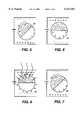
- FIG. 2is a diagram of the charges on a ball having a photoconducting black hemisphere in the initial electric field.
- FIG. 3is a diagram of the charges on a ball having a conducting white hemisphere after radiation.
- FIG. 4is a diagram of the charges on a ball having a conducting white hemisphere after radiation and field reversal.
- FIG. 5is a diagram of the charges on a ball having an insulating white hemisphere in the initial electric field.
- FIG. 6is a diagram of the charges on a ball having an insulating white hemisphere after radiation.
- FIG. 7is a diagram of the charges on a ball having an insulating white hemisphere after radiation and field reversal.
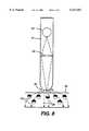
- FIG. 8is an embodiment which uses a stylus to write an image in the form of a line on the medium.
- FIG. 9is an embodiment which uses a stylus to write an image in the form of a series of linear elements on the medium.
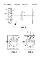
- FIG. 1A source of light is generated by element 10 and is focussed on the Electric paper sheet 11 by a lens 12. In the case of X-radiation the lens would not be necessary.
- the sheet of Electric paperconsists of a number of balls 13, one of which is shown as a magnified ball 17.
- one hemispherewill be made of a white insulative material, such as titanium dioxide dispersed in polyethylene.
- the other hemispherewill be photosensitive, and of a contrasting color.
- photosensitivityThere are many types of photosensitivity that can be incorporated in the behavior of this hemisphere, but for the purposes of illustration we will limit these to the two major classes of photoconductive and photoinjective behavior.
- one hemisphere of the bichromal ballresponds electrically to light exposure the corresponding change in surface charge density will superimpose on the dark surface charge condition, resulting in a change in the electrical behavior of the bichromal ball upon exposure to actinic radiation.
- a uniform electrical fieldis applied at the surfaces 14 to orient all of the balls in one direction and then actinic radiation is applied and the field reversed to orient either only the exposed balls or only the unexposed balls in the other direction, producing a stored image.
- the ball rotation upon actinic light exposuremay take place without the change in field direction.
- the entire ball or just the photosensitive hemisphere of the ballmay be made from a material, such as PVK (poly-n-vinyl-carbazole) that easily transports photogenerated carriers. It may be sensitized for the actinic radiation by the addition of certain dyes (such as tri-n-nitrol-fluorenone) to make it photoconducting or it may be overcoated by a photogenerating layer, such as selenium that will produce photogenerated carriers that are injected into and conducted by the carrier transporting material.
- PVKpoly-n-vinyl-carbazole
- a photogenerating layersuch as selenium that will produce photogenerated carriers that are injected into and conducted by the carrier transporting material.
- the ball or the photosensitive hemispheremay also be made from an insulative material such as epoxy or polyethylene pigmented by photoconductive materials such as cadmium sulfide.
- the photoconductorIn the case where X-Ray images are to recorded, the photoconductor will typically be made from elements having high atomic number. Thus selenium and lead oxide are widely used photoconductors for this purpose.
- a less well known but very suitable photosensitive processutilizes the photoinjection of carriers from a photoconductor, such as selenium, into a surrounding dielectric liquid.
- a photoconductorsuch as selenium
- one hemisphere of a bichromal ball made from insulative materialis coated with a thin selenium layer (by evaporation, for example) it will exhibit this behavior.
- photogenerated carrierswill be injected into the plasticizing liquid from the selenium and will be transported away from the surface, leaving it with a net charge.
- Another photosensitive mechanismis derived from the surface photoeffect.
- Many semiconductor materialsexhibit a charge redistribution upon exposure to actinic light as charges trapped near the surface are driven into the bulk of the material. The re-distribution of charge results in a measureable change in the electrostatic potential at the surface. This change is known as the surface photovoltage.
- This change in surface potentialalso results in a change in dipole moment.
- titanium dioxidehas been observed to change its surface potential by several volts upon exposure to modest light levels. This material is particularly interesting because it is also a white pigment.
- one side of a bichromal ball which contains such a pigmentwill also have an intrinsically photosensitive dipole moment.
- the photoresponsive rotation of the bichromal ballsdepends upon the structure of the balls.
- the ballsare generally contained within spherical cavities filled with dielectric liquid.
- Upon the application of an electrical field theywill both rotate as a dipole and translate as a monopole.
- the dipole behaviordepends upon the difference in surface charge between the two hemispheres of the balls.
- the monopole behaviordepends upon the sum of the surface charges. Thus, equal positive and negative charges on the hemispheres will create a dipole with resulting rotation in a uniform electrical field, but there will be no monopole and thus no linear motion. Most commonly there is both a dipole and a monopole behavior.
- the monopole behaviordrives the ball into the cavity wall where intimate contact allows van der Wahl and other forces to operate and create an adhesion of the ball to the wall. This creates a threshold behavior. Voltages applied to the bichromal ball below a certain value will not cause rotation whereas voltages above a certain value will. Generally, smaller balls require lower voltages to rotate.
- Grey scale responsecan be obtained by using bichromal balls with a range of diameters, or balls with a range of photoconductive response. (Smaller bichromal balls will rotate at lower threshold voltages, in general.)
- the bichromal ballswill be aligned by the uniform external field and while this voltage continues to be applied the actinic radiation exposure will take place. If the (typically) selenium coated hemisphere is also the initially positively charged hemisphere the same behavior as described above will obtain. If, however, this is the initially negatively charged hemisphere, the photoinjection of negative charges into the plasticizing liquid will cause the charge on this hemisphere to decrease and eventually become positive. Hence the bichromal balls might rotate after a given exposure without a reversal in the field; simply after sufficient exposure.
- the two hemispheres of the bichromal ballscould each have photosensitive properties. If one had ordinary photoconductor properties and the other had the photoinjection type of property described in the latter half of the above paragraph, both sequential exposure to two different images and simultaneous exposure to two images received through the two sides of the display would result in a recorded image that was the pixel by pixel difference of the two input images. This property is useful for such applications as change detection.
- a stylusis used to write an image on the display medium.
- This embodimentis shown in FIG. 8.
- the stylus 21contains an electrode 22 at its tip for applying the electric field to the medium 25.
- This fieldis applied only in the region of the stylus, and is thus used to alter the image in that region, and would be used in a manner similar to that of a conventional pen writing on a piece of paper. It is an unavoidable fact that such an electrode will exhibit a fringe field extending around the stylus.
- the field directly below the stylus 26has a direction which is substantially normal to the plane of the paper, the fringe field 27 necessarily has a direction away from the normal, and is thus undesirable as it will cause improper rotation of balls.
- FIG. 9shows an extension of this idea to a writing method using an automated scan bar which is moved across the medium.
- the scan bar 31contains an extended light source 33, with suitable focusing means 34.
- the electrode array 32is then driven by suitable electronics in such a manner as to generate one linear element of the desired image. By moving the scan bar across the medium, the complete image is formed.
Landscapes
- Physics & Mathematics (AREA)
- General Physics & Mathematics (AREA)
- Health & Medical Sciences (AREA)
- Life Sciences & Earth Sciences (AREA)
- Molecular Biology (AREA)
- Optics & Photonics (AREA)
- Engineering & Computer Science (AREA)
- Theoretical Computer Science (AREA)
- Electrochromic Elements, Electrophoresis, Or Variable Reflection Or Absorption Elements (AREA)
- Devices For Indicating Variable Information By Combining Individual Elements (AREA)
Abstract
Description
Claims (8)
Priority Applications (4)
| Application Number | Priority Date | Filing Date | Title |
|---|---|---|---|
| US08/368,133US6137467A (en) | 1995-01-03 | 1995-01-03 | Optically sensitive electric paper |
| JP7343131AJPH08234685A (en) | 1995-01-03 | 1995-12-28 | Device for generation of picture from light source |
| EP96300062AEP0721177B1 (en) | 1995-01-03 | 1996-01-03 | Apparatus for generating an image from a light source and a display medium for displaying an image |
| DE69612404TDE69612404T2 (en) | 1995-01-03 | 1996-01-03 | Device for generating an image from a light source and display medium for displaying an image |
Applications Claiming Priority (1)
| Application Number | Priority Date | Filing Date | Title |
|---|---|---|---|
| US08/368,133US6137467A (en) | 1995-01-03 | 1995-01-03 | Optically sensitive electric paper |
Publications (1)
| Publication Number | Publication Date |
|---|---|
| US6137467Atrue US6137467A (en) | 2000-10-24 |
Family
ID=23449980
Family Applications (1)
| Application Number | Title | Priority Date | Filing Date |
|---|---|---|---|
| US08/368,133Expired - Fee RelatedUS6137467A (en) | 1995-01-03 | 1995-01-03 | Optically sensitive electric paper |
Country Status (4)
| Country | Link |
|---|---|
| US (1) | US6137467A (en) |
| EP (1) | EP0721177B1 (en) |
| JP (1) | JPH08234685A (en) |
| DE (1) | DE69612404T2 (en) |
Cited By (273)
| Publication number | Priority date | Publication date | Assignee | Title |
|---|---|---|---|---|
| US20020021270A1 (en)* | 2000-08-17 | 2002-02-21 | Albert Jonathan D. | Bistable electro-optic desplay, and method for addressing same |
| US20020057250A1 (en)* | 2000-08-21 | 2002-05-16 | Michaelis A. John | Methods and apparatus for imaging electronic paper |
| US6440252B1 (en) | 1999-12-17 | 2002-08-27 | Xerox Corporation | Method for rotatable element assembly |
| US20020126261A1 (en)* | 2000-11-29 | 2002-09-12 | Matsushita Electric Industrial Co., Ltd. | Display device and method for manufacturing the same |
| US20020130832A1 (en)* | 2001-03-13 | 2002-09-19 | Baucom Allan Scott | Apparatus for displaying drawings |
| US6473072B1 (en)* | 1998-05-12 | 2002-10-29 | E Ink Corporation | Microencapsulated electrophoretic electrostatically-addressed media for drawing device applications |
| US20020191133A1 (en)* | 2000-09-14 | 2002-12-19 | Kabushiki Kaisha Toshiba | Reflective display |
| US6498674B1 (en) | 2000-04-14 | 2002-12-24 | Xerox Corporation | Rotating element sheet material with generalized containment structure |
| US6504525B1 (en) | 2000-05-03 | 2003-01-07 | Xerox Corporation | Rotating element sheet material with microstructured substrate and method of use |
| US20030011867A1 (en)* | 2001-07-09 | 2003-01-16 | Loxley Andrew L. | Electro-optic display and adhesive composition for use therein |
| US20030011560A1 (en)* | 1998-08-27 | 2003-01-16 | E Ink Corporation | Electrophoretic display comprising optical biasing element |
| US20030011868A1 (en)* | 1998-03-18 | 2003-01-16 | E Ink Corporation | Electrophoretic displays in portable devices and systems for addressing such displays |
| US20030025855A1 (en)* | 2001-07-09 | 2003-02-06 | E Lnk Corporation | Electro-optic display and lamination adhesive |
| US20030053189A1 (en)* | 2001-09-14 | 2003-03-20 | E Ink Corporation | Methods for addressing electro-optic materials |
| US6545671B1 (en) | 2000-03-02 | 2003-04-08 | Xerox Corporation | Rotating element sheet material with reversible highlighting |
| US20030137521A1 (en)* | 1999-04-30 | 2003-07-24 | E Ink Corporation | Methods for driving bistable electro-optic displays, and apparatus for use therein |
| US20030214695A1 (en)* | 2002-03-18 | 2003-11-20 | E Ink Corporation | Electro-optic displays, and methods for driving same |
| WO2003107315A2 (en) | 2002-06-13 | 2003-12-24 | E Ink Corporation | Methods for driving electro-optic displays |
| US20040012849A1 (en)* | 2001-03-22 | 2004-01-22 | Cruz-Uribe Antonio S. | Enhanced contrast projection screen |
| US20040012839A1 (en)* | 2002-05-23 | 2004-01-22 | E Ink Corporation | Capsules, materials for use therein and electrophoretic media and displays containing such capsules |
| US20040014265A1 (en)* | 2002-04-24 | 2004-01-22 | E Ink Corporation | Processes for forming backplanes for electro-optic displays |
| US6690350B2 (en) | 2001-01-11 | 2004-02-10 | Xerox Corporation | Rotating element sheet material with dual vector field addressing |
| US20040027327A1 (en)* | 2002-06-10 | 2004-02-12 | E Ink Corporation | Components and methods for use in electro-optic displays |
| US6704133B2 (en) | 1998-03-18 | 2004-03-09 | E-Ink Corporation | Electro-optic display overlays and systems for addressing such displays |
| US20040112750A1 (en)* | 2002-09-03 | 2004-06-17 | E Ink Corporation | Electrophoretic medium with gaseous suspending fluid |
| US20040136048A1 (en)* | 1995-07-20 | 2004-07-15 | E Ink Corporation | Dielectrophoretic displays |
| US20040155857A1 (en)* | 2002-09-03 | 2004-08-12 | E Ink Corporation | Electro-optic displays |
| US20040233509A1 (en)* | 2002-12-23 | 2004-11-25 | E Ink Corporation | Flexible electro-optic displays |
| US6839158B2 (en) | 1997-08-28 | 2005-01-04 | E Ink Corporation | Encapsulated electrophoretic displays having a monolayer of capsules and materials and methods for making the same |
| US20050007336A1 (en)* | 1997-08-28 | 2005-01-13 | E Ink Corporation | Adhesive backed displays |
| US6847347B1 (en) | 2000-08-17 | 2005-01-25 | Xerox Corporation | Electromagnetophoretic display system and method |
| US6864875B2 (en) | 1998-04-10 | 2005-03-08 | E Ink Corporation | Full color reflective display with multichromatic sub-pixels |
| US6897848B2 (en) | 2001-01-11 | 2005-05-24 | Xerox Corporation | Rotating element sheet material and stylus with gradient field addressing |
| WO2005054933A2 (en) | 2003-11-26 | 2005-06-16 | E Ink Corporation | Electro-optic displays with reduced remnant voltage |
| US6970154B2 (en) | 2001-01-11 | 2005-11-29 | Jpmorgan Chase Bank | Fringe-field filter for addressable displays |
| US6987603B2 (en) | 2003-01-31 | 2006-01-17 | E Ink Corporation | Construction of electrophoretic displays |
| US7002728B2 (en) | 1997-08-28 | 2006-02-21 | E Ink Corporation | Electrophoretic particles, and processes for the production thereof |
| US7012735B2 (en) | 2003-03-27 | 2006-03-14 | E Ink Corporaiton | Electro-optic assemblies, and materials for use therein |
| US7034783B2 (en) | 2003-08-19 | 2006-04-25 | E Ink Corporation | Method for controlling electro-optic display |
| US7071913B2 (en) | 1995-07-20 | 2006-07-04 | E Ink Corporation | Retroreflective electrophoretic displays and materials for making the same |
| US7075703B2 (en) | 2004-01-16 | 2006-07-11 | E Ink Corporation | Process for sealing electro-optic displays |
| US7079305B2 (en) | 2001-03-19 | 2006-07-18 | E Ink Corporation | Electrophoretic medium and process for the production thereof |
| US7110163B2 (en) | 2001-07-09 | 2006-09-19 | E Ink Corporation | Electro-optic display and lamination adhesive for use therein |
| US7110164B2 (en) | 2002-06-10 | 2006-09-19 | E Ink Corporation | Electro-optic displays, and processes for the production thereof |
| US7116318B2 (en) | 2002-04-24 | 2006-10-03 | E Ink Corporation | Backplanes for display applications, and components for use therein |
| US7116466B2 (en) | 2004-07-27 | 2006-10-03 | E Ink Corporation | Electro-optic displays |
| US7119772B2 (en) | 1999-04-30 | 2006-10-10 | E Ink Corporation | Methods for driving bistable electro-optic displays, and apparatus for use therein |
| US7119759B2 (en) | 1999-05-03 | 2006-10-10 | E Ink Corporation | Machine-readable displays |
| US7167155B1 (en) | 1995-07-20 | 2007-01-23 | E Ink Corporation | Color electrophoretic displays |
| US7173752B2 (en) | 2003-11-05 | 2007-02-06 | E Ink Corporation | Electro-optic displays, and materials for use therein |
| US7176880B2 (en) | 1999-07-21 | 2007-02-13 | E Ink Corporation | Use of a storage capacitor to enhance the performance of an active matrix driven electronic display |
| US7190008B2 (en) | 2002-04-24 | 2007-03-13 | E Ink Corporation | Electro-optic displays, and components for use therein |
| US7193625B2 (en) | 1999-04-30 | 2007-03-20 | E Ink Corporation | Methods for driving electro-optic displays, and apparatus for use therein |
| US7206119B2 (en) | 2003-12-31 | 2007-04-17 | E Ink Corporation | Electro-optic displays, and method for driving same |
| US7230751B2 (en) | 2005-01-26 | 2007-06-12 | E Ink Corporation | Electrophoretic displays using gaseous fluids |
| US7230750B2 (en) | 2001-05-15 | 2007-06-12 | E Ink Corporation | Electrophoretic media and processes for the production thereof |
| US7242513B2 (en) | 1997-08-28 | 2007-07-10 | E Ink Corporation | Encapsulated electrophoretic displays having a monolayer of capsules and materials and methods for making the same |
| US7247379B2 (en) | 1997-08-28 | 2007-07-24 | E Ink Corporation | Electrophoretic particles, and processes for the production thereof |
| WO2007104003A2 (en) | 2006-03-08 | 2007-09-13 | E Ink Corporation | Methods for production of electro-optic displays |
| US7312916B2 (en) | 2002-08-07 | 2007-12-25 | E Ink Corporation | Electrophoretic media containing specularly reflective particles |
| US7327511B2 (en) | 2004-03-23 | 2008-02-05 | E Ink Corporation | Light modulators |
| US7339715B2 (en) | 2003-03-25 | 2008-03-04 | E Ink Corporation | Processes for the production of electrophoretic displays |
| US7365394B2 (en) | 2000-04-18 | 2008-04-29 | E Ink Corporation | Process for fabricating thin film transistors |
| US7365733B2 (en) | 2002-12-16 | 2008-04-29 | E Ink Corporation | Backplanes for electro-optic displays |
| US20080117495A1 (en)* | 1995-07-20 | 2008-05-22 | E Ink Corporation | Dielectrophoretic displays |
| US7382363B2 (en) | 2001-07-27 | 2008-06-03 | E Ink Corporation | Microencapsulated electrophoretic display with integrated driver |
| US7388572B2 (en) | 2004-02-27 | 2008-06-17 | E Ink Corporation | Backplanes for electro-optic displays |
| US7411720B2 (en) | 2001-05-15 | 2008-08-12 | E Ink Corporation | Electrophoretic particles and processes for the production thereof |
| US7411719B2 (en) | 1995-07-20 | 2008-08-12 | E Ink Corporation | Electrophoretic medium and process for the production thereof |
| US7420549B2 (en) | 2003-10-08 | 2008-09-02 | E Ink Corporation | Electro-wetting displays |
| US20080211765A1 (en)* | 1995-07-20 | 2008-09-04 | E Ink Corporation | Stylus-based addressing structures for displays |
| US7453445B2 (en) | 2004-08-13 | 2008-11-18 | E Ink Corproation | Methods for driving electro-optic displays |
| US7477444B2 (en) | 2006-09-22 | 2009-01-13 | E Ink Corporation & Air Products And Chemical, Inc. | Electro-optic display and materials for use therein |
| US20090027762A1 (en)* | 1995-07-20 | 2009-01-29 | E Ink Corporation | Electro-osmotic displays and materials for making the same |
| US7492497B2 (en) | 2006-08-02 | 2009-02-17 | E Ink Corporation | Multi-layer light modulator |
| US7492339B2 (en) | 2004-03-26 | 2009-02-17 | E Ink Corporation | Methods for driving bistable electro-optic displays |
| US7528822B2 (en) | 2001-11-20 | 2009-05-05 | E Ink Corporation | Methods for driving electro-optic displays |
| US7535624B2 (en) | 2001-07-09 | 2009-05-19 | E Ink Corporation | Electro-optic display and materials for use therein |
| US7551346B2 (en) | 2003-11-05 | 2009-06-23 | E Ink Corporation | Electro-optic displays, and materials for use therein |
| US7554712B2 (en) | 2005-06-23 | 2009-06-30 | E Ink Corporation | Edge seals for, and processes for assembly of, electro-optic displays |
| US7583427B2 (en) | 2002-06-10 | 2009-09-01 | E Ink Corporation | Components and methods for use in electro-optic displays |
| US7602374B2 (en) | 2003-09-19 | 2009-10-13 | E Ink Corporation | Methods for reducing edge effects in electro-optic displays |
| US20090256868A1 (en)* | 2008-04-11 | 2009-10-15 | Yun Shon Low | Time-Overlapping Partial-Panel Updating Of A Bistable Electro-Optic Display |
| US7636191B2 (en) | 2003-07-24 | 2009-12-22 | E Ink Corporation | Electro-optic display |
| US7649666B2 (en) | 2006-12-07 | 2010-01-19 | E Ink Corporation | Components and methods for use in electro-optic displays |
| US7649674B2 (en) | 2002-06-10 | 2010-01-19 | E Ink Corporation | Electro-optic display with edge seal |
| US7667886B2 (en) | 2007-01-22 | 2010-02-23 | E Ink Corporation | Multi-layer sheet for use in electro-optic displays |
| US7672040B2 (en) | 2003-11-05 | 2010-03-02 | E Ink Corporation | Electro-optic displays, and materials for use therein |
| US7679814B2 (en) | 2001-04-02 | 2010-03-16 | E Ink Corporation | Materials for use in electrophoretic displays |
| US7688497B2 (en) | 2007-01-22 | 2010-03-30 | E Ink Corporation | Multi-layer sheet for use in electro-optic displays |
| US7826129B2 (en) | 2007-03-06 | 2010-11-02 | E Ink Corporation | Materials for use in electrophoretic displays |
| US20100283806A1 (en)* | 1997-08-28 | 2010-11-11 | E Ink Corporation | Multi-color electrophoretic displays and materials for making the same |
| US20100289026A1 (en)* | 2006-07-04 | 2010-11-18 | Semiconductor Energy Laboratory Co., Ltd. | Method for Manufacturing Display Device |
| US7839564B2 (en) | 2002-09-03 | 2010-11-23 | E Ink Corporation | Components and methods for use in electro-optic displays |
| US7843621B2 (en) | 2002-06-10 | 2010-11-30 | E Ink Corporation | Components and testing methods for use in the production of electro-optic displays |
| US7843624B2 (en) | 2006-03-08 | 2010-11-30 | E Ink Corporation | Electro-optic displays, and materials and methods for production thereof |
| US7848006B2 (en) | 1995-07-20 | 2010-12-07 | E Ink Corporation | Electrophoretic displays with controlled amounts of pigment |
| US7893435B2 (en) | 2000-04-18 | 2011-02-22 | E Ink Corporation | Flexible electronic circuits and displays including a backplane comprising a patterned metal foil having a plurality of apertures extending therethrough |
| US7903319B2 (en) | 2006-07-11 | 2011-03-08 | E Ink Corporation | Electrophoretic medium and display with improved image stability |
| US7910175B2 (en) | 2003-03-25 | 2011-03-22 | E Ink Corporation | Processes for the production of electrophoretic displays |
| US7952790B2 (en) | 2006-03-22 | 2011-05-31 | E Ink Corporation | Electro-optic media produced using ink jet printing |
| US7952557B2 (en) | 2001-11-20 | 2011-05-31 | E Ink Corporation | Methods and apparatus for driving electro-optic displays |
| US7956841B2 (en) | 1995-07-20 | 2011-06-07 | E Ink Corporation | Stylus-based addressing structures for displays |
| US7986450B2 (en) | 2006-09-22 | 2011-07-26 | E Ink Corporation | Electro-optic display and materials for use therein |
| US7999787B2 (en) | 1995-07-20 | 2011-08-16 | E Ink Corporation | Methods for driving electrophoretic displays using dielectrophoretic forces |
| US8009348B2 (en) | 1999-05-03 | 2011-08-30 | E Ink Corporation | Machine-readable displays |
| US8018640B2 (en) | 2006-07-13 | 2011-09-13 | E Ink Corporation | Particles for use in electrophoretic displays |
| US8034209B2 (en) | 2007-06-29 | 2011-10-11 | E Ink Corporation | Electro-optic displays, and materials and methods for production thereof |
| US8040594B2 (en) | 1997-08-28 | 2011-10-18 | E Ink Corporation | Multi-color electrophoretic displays |
| US8049947B2 (en) | 2002-06-10 | 2011-11-01 | E Ink Corporation | Components and methods for use in electro-optic displays |
| US8054526B2 (en) | 2008-03-21 | 2011-11-08 | E Ink Corporation | Electro-optic displays, and color filters for use therein |
| US8098418B2 (en) | 2009-03-03 | 2012-01-17 | E. Ink Corporation | Electro-optic displays, and color filters for use therein |
| US8115729B2 (en) | 1999-05-03 | 2012-02-14 | E Ink Corporation | Electrophoretic display element with filler particles |
| US8125501B2 (en) | 2001-11-20 | 2012-02-28 | E Ink Corporation | Voltage modulated driver circuits for electro-optic displays |
| US8139050B2 (en) | 1995-07-20 | 2012-03-20 | E Ink Corporation | Addressing schemes for electronic displays |
| US8174490B2 (en) | 2003-06-30 | 2012-05-08 | E Ink Corporation | Methods for driving electrophoretic displays |
| US8177942B2 (en) | 2003-11-05 | 2012-05-15 | E Ink Corporation | Electro-optic displays, and materials for use therein |
| EP2487540A1 (en) | 2006-09-18 | 2012-08-15 | E-Ink Corporation | Color electro-optic displays |
| US8270064B2 (en) | 2009-02-09 | 2012-09-18 | E Ink Corporation | Electrophoretic particles, and processes for the production thereof |
| US8289250B2 (en) | 2004-03-31 | 2012-10-16 | E Ink Corporation | Methods for driving electro-optic displays |
| US8314784B2 (en) | 2008-04-11 | 2012-11-20 | E Ink Corporation | Methods for driving electro-optic displays |
| CN102789764A (en)* | 2001-11-20 | 2012-11-21 | 伊英克公司 | Methods for driving bistable electro-optic displays |
| US8319759B2 (en) | 2003-10-08 | 2012-11-27 | E Ink Corporation | Electrowetting displays |
| US8363299B2 (en) | 2002-06-10 | 2013-01-29 | E Ink Corporation | Electro-optic displays, and processes for the production thereof |
| US8390918B2 (en) | 2001-04-02 | 2013-03-05 | E Ink Corporation | Electrophoretic displays with controlled amounts of pigment |
| US8390301B2 (en) | 2006-03-08 | 2013-03-05 | E Ink Corporation | Electro-optic displays, and materials and methods for production thereof |
| US8446664B2 (en) | 2010-04-02 | 2013-05-21 | E Ink Corporation | Electrophoretic media, and materials for use therein |
| US8558783B2 (en) | 2001-11-20 | 2013-10-15 | E Ink Corporation | Electro-optic displays with reduced remnant voltage |
| US8576476B2 (en) | 2010-05-21 | 2013-11-05 | E Ink Corporation | Multi-color electro-optic displays |
| US8576470B2 (en) | 2010-06-02 | 2013-11-05 | E Ink Corporation | Electro-optic displays, and color alters for use therein |
| US8593396B2 (en) | 2001-11-20 | 2013-11-26 | E Ink Corporation | Methods and apparatus for driving electro-optic displays |
| US8610988B2 (en) | 2006-03-09 | 2013-12-17 | E Ink Corporation | Electro-optic display with edge seal |
| US8654436B1 (en) | 2009-10-30 | 2014-02-18 | E Ink Corporation | Particles for use in electrophoretic displays |
| EP2711770A2 (en) | 2005-10-18 | 2014-03-26 | E Ink Corporation | Components for electro-optic displays |
| US8754859B2 (en) | 2009-10-28 | 2014-06-17 | E Ink Corporation | Electro-optic displays with touch sensors and/or tactile feedback |
| US8873129B2 (en) | 2011-04-07 | 2014-10-28 | E Ink Corporation | Tetrachromatic color filter array for reflective display |
| US8902153B2 (en) | 2007-08-03 | 2014-12-02 | E Ink Corporation | Electro-optic displays, and processes for their production |
| US8928562B2 (en) | 2003-11-25 | 2015-01-06 | E Ink Corporation | Electro-optic displays, and methods for driving same |
| US9005494B2 (en) | 2004-01-20 | 2015-04-14 | E Ink Corporation | Preparation of capsules |
| US9170467B2 (en) | 2005-10-18 | 2015-10-27 | E Ink Corporation | Color electro-optic displays, and processes for the production thereof |
| US9195111B2 (en) | 2013-02-11 | 2015-11-24 | E Ink Corporation | Patterned electro-optic displays and processes for the production thereof |
| EP2947647A2 (en) | 2003-06-30 | 2015-11-25 | E Ink Corporation | Methods for driving electro-optic displays |
| US9199441B2 (en) | 2007-06-28 | 2015-12-01 | E Ink Corporation | Processes for the production of electro-optic displays, and color filters for use therein |
| US9230492B2 (en) | 2003-03-31 | 2016-01-05 | E Ink Corporation | Methods for driving electro-optic displays |
| US9238340B2 (en) | 2012-07-27 | 2016-01-19 | E Ink Corporation | Processes for the production of electro-optic displays |
| US9293511B2 (en) | 1998-07-08 | 2016-03-22 | E Ink Corporation | Methods for achieving improved color in microencapsulated electrophoretic devices |
| US9412314B2 (en) | 2001-11-20 | 2016-08-09 | E Ink Corporation | Methods for driving electro-optic displays |
| US9436056B2 (en) | 2013-02-06 | 2016-09-06 | E Ink Corporation | Color electro-optic displays |
| US9470950B2 (en) | 2002-06-10 | 2016-10-18 | E Ink Corporation | Electro-optic displays, and processes for the production thereof |
| US9495918B2 (en) | 2013-03-01 | 2016-11-15 | E Ink Corporation | Methods for driving electro-optic displays |
| US20160351131A1 (en)* | 2015-05-27 | 2016-12-01 | E Ink Corporation | Methods and circuitry for driving display devices |
| US9513743B2 (en) | 2012-06-01 | 2016-12-06 | E Ink Corporation | Methods for driving electro-optic displays |
| US9529240B2 (en) | 2014-01-17 | 2016-12-27 | E Ink Corporation | Controlled polymeric material conductivity for use in a two-phase electrode layer |
| US9530363B2 (en) | 2001-11-20 | 2016-12-27 | E Ink Corporation | Methods and apparatus for driving electro-optic displays |
| WO2017049020A1 (en) | 2015-09-16 | 2017-03-23 | E Ink Corporation | Apparatus and methods for driving displays |
| US9620066B2 (en) | 2010-02-02 | 2017-04-11 | E Ink Corporation | Method for driving electro-optic displays |
| US9620048B2 (en) | 2013-07-30 | 2017-04-11 | E Ink Corporation | Methods for driving electro-optic displays |
| US9664978B2 (en) | 2002-10-16 | 2017-05-30 | E Ink Corporation | Electrophoretic displays |
| US9671635B2 (en) | 2014-02-07 | 2017-06-06 | E Ink Corporation | Electro-optic display backplane structures with drive components and pixel electrodes on opposed surfaces |
| US9672766B2 (en) | 2003-03-31 | 2017-06-06 | E Ink Corporation | Methods for driving electro-optic displays |
| US9715155B1 (en) | 2013-01-10 | 2017-07-25 | E Ink Corporation | Electrode structures for electro-optic displays |
| US9721495B2 (en) | 2013-02-27 | 2017-08-01 | E Ink Corporation | Methods for driving electro-optic displays |
| US9726957B2 (en) | 2013-01-10 | 2017-08-08 | E Ink Corporation | Electro-optic display with controlled electrochemical reactions |
| WO2017139323A1 (en) | 2016-02-08 | 2017-08-17 | E Ink Corporation | Methods and apparatus for operating an electro-optic display in white mode |
| EP3220383A1 (en) | 2012-02-01 | 2017-09-20 | E Ink Corporation | Methods for driving electro-optic displays |
| US9777201B2 (en) | 2015-07-23 | 2017-10-03 | E Ink Corporation | Polymer formulations for use with electro-optic media |
| US9835925B1 (en) | 2015-01-08 | 2017-12-05 | E Ink Corporation | Electro-optic displays, and processes for the production thereof |
| US9880646B2 (en) | 2015-02-18 | 2018-01-30 | E Ink Corporation | Addressable electro-optic display |
| US9928810B2 (en) | 2015-01-30 | 2018-03-27 | E Ink Corporation | Font control for electro-optic displays and related apparatus and methods |
| US9964831B2 (en) | 2007-11-14 | 2018-05-08 | E Ink Corporation | Electro-optic assemblies, and adhesives and binders for use therein |
| US9966018B2 (en) | 2002-06-13 | 2018-05-08 | E Ink Corporation | Methods for driving electro-optic displays |
| WO2018102126A1 (en) | 2016-11-30 | 2018-06-07 | E Ink Corporation | Laminated electro-optic displays and methods of making the same |
| US10037735B2 (en) | 2012-11-16 | 2018-07-31 | E Ink Corporation | Active matrix display with dual driving modes |
| US10037089B2 (en) | 2015-02-17 | 2018-07-31 | E Ink Corporation | Electromagnetic writing apparatus for electro-optic displays |
| US10048564B2 (en) | 2003-11-05 | 2018-08-14 | E Ink Corporation | Electro-optic displays, and materials for use therein |
| US10146261B2 (en) | 2016-08-08 | 2018-12-04 | E Ink Corporation | Wearable apparatus having a flexible electrophoretic display |
| US10163406B2 (en) | 2015-02-04 | 2018-12-25 | E Ink Corporation | Electro-optic displays displaying in dark mode and light mode, and related apparatus and methods |
| US10174232B2 (en) | 2015-09-30 | 2019-01-08 | E Ink Corporation | Polyurethane adhesive layers for electro-optic assemblies |
| US10175550B2 (en) | 2014-11-07 | 2019-01-08 | E Ink Corporation | Applications of electro-optic displays |
| US10190743B2 (en) | 2012-04-20 | 2019-01-29 | E Ink Corporation | Illumination systems for reflective displays |
| US10197883B2 (en) | 2015-01-05 | 2019-02-05 | E Ink Corporation | Electro-optic displays, and methods for driving same |
| US10254620B1 (en) | 2016-03-08 | 2019-04-09 | E Ink Corporation | Encapsulated photoelectrophoretic display |
| US10282033B2 (en) | 2012-06-01 | 2019-05-07 | E Ink Corporation | Methods for updating electro-optic displays when drawing or writing on the display |
| US10317767B2 (en) | 2014-02-07 | 2019-06-11 | E Ink Corporation | Electro-optic display backplane structure with drive components and pixel electrodes on opposed surfaces |
| US10319313B2 (en) | 2007-05-21 | 2019-06-11 | E Ink Corporation | Methods for driving video electro-optic displays |
| US10324577B2 (en) | 2017-02-28 | 2019-06-18 | E Ink Corporation | Writeable electrophoretic displays including sensing circuits and styli configured to interact with sensing circuits |
| US10353266B2 (en) | 2014-09-26 | 2019-07-16 | E Ink Corporation | Color sets for low resolution dithering in reflective color displays |
| WO2019144097A1 (en) | 2018-01-22 | 2019-07-25 | E Ink Corporation | Electro-optic displays, and methods for driving same |
| US10372008B2 (en) | 2011-05-21 | 2019-08-06 | E Ink Corporation | Electro-optic displays |
| US10388233B2 (en) | 2015-08-31 | 2019-08-20 | E Ink Corporation | Devices and techniques for electronically erasing a drawing device |
| US10446585B2 (en) | 2014-03-17 | 2019-10-15 | E Ink Corporation | Multi-layer expanding electrode structures for backplane assemblies |
| US10444592B2 (en) | 2017-03-09 | 2019-10-15 | E Ink Corporation | Methods and systems for transforming RGB image data to a reduced color set for electro-optic displays |
| US10467984B2 (en) | 2017-03-06 | 2019-11-05 | E Ink Corporation | Method for rendering color images |
| US10466565B2 (en) | 2017-03-28 | 2019-11-05 | E Ink Corporation | Porous backplane for electro-optic display |
| US10475396B2 (en) | 2015-02-04 | 2019-11-12 | E Ink Corporation | Electro-optic displays with reduced remnant voltage, and related apparatus and methods |
| US10495941B2 (en) | 2017-05-19 | 2019-12-03 | E Ink Corporation | Foldable electro-optic display including digitization and touch sensing |
| US10509294B2 (en) | 2017-01-25 | 2019-12-17 | E Ink Corporation | Dual sided electrophoretic display |
| WO2020033176A1 (en) | 2018-08-07 | 2020-02-13 | E Ink Corporation | Flexible encapsulated electro-optic media |
| US10573222B2 (en) | 2015-01-05 | 2020-02-25 | E Ink Corporation | Electro-optic displays, and methods for driving same |
| US10573257B2 (en) | 2017-05-30 | 2020-02-25 | E Ink Corporation | Electro-optic displays |
| US10670892B2 (en) | 2016-04-22 | 2020-06-02 | E Ink Corporation | Foldable electro-optic display apparatus |
| US10726798B2 (en) | 2003-03-31 | 2020-07-28 | E Ink Corporation | Methods for operating electro-optic displays |
| US10803813B2 (en) | 2015-09-16 | 2020-10-13 | E Ink Corporation | Apparatus and methods for driving displays |
| US10824042B1 (en) | 2017-10-27 | 2020-11-03 | E Ink Corporation | Electro-optic display and composite materials having low thermal sensitivity for use therein |
| US10832622B2 (en) | 2017-04-04 | 2020-11-10 | E Ink Corporation | Methods for driving electro-optic displays |
| US10852568B2 (en) | 2017-03-03 | 2020-12-01 | E Ink Corporation | Electro-optic displays and driving methods |
| US10962816B2 (en) | 2017-06-16 | 2021-03-30 | E Ink Corporation | Flexible color-changing fibers and fabrics |
| WO2021071600A1 (en) | 2019-10-07 | 2021-04-15 | E Ink Corporation | An adhesive composition comprising a polyurethane and a cationic dopant |
| US11030936B2 (en) | 2012-02-01 | 2021-06-08 | E Ink Corporation | Methods and apparatus for operating an electro-optic display in white mode |
| US11030969B2 (en) | 2019-03-29 | 2021-06-08 | E Ink Corporation | Electro-optic displays and methods of driving the same |
| WO2021133541A1 (en) | 2019-12-23 | 2021-07-01 | E Ink Corporation | Transferable light-transmissive electrode films for electro-optic devices |
| US11062663B2 (en) | 2018-11-30 | 2021-07-13 | E Ink California, Llc | Electro-optic displays and driving methods |
| US11081066B2 (en) | 2018-02-15 | 2021-08-03 | E Ink Corporation | Via placement for slim border electro-optic display backplanes with decreased capacitive coupling between t-wires and pixel electrodes |
| US11079651B2 (en) | 2017-12-15 | 2021-08-03 | E Ink Corporation | Multi-color electro-optic media |
| US11139594B2 (en) | 2019-04-30 | 2021-10-05 | E Ink Corporation | Connectors for electro-optic displays |
| US11143929B2 (en) | 2018-03-09 | 2021-10-12 | E Ink Corporation | Reflective electrophoretic displays including photo-luminescent material and color filter arrays |
| US11181799B2 (en) | 2018-05-17 | 2021-11-23 | E Ink California, Llc | Piezo electrophoretic display |
| US11195480B2 (en) | 2013-07-31 | 2021-12-07 | E Ink Corporation | Partial update driving methods for bistable electro-optic displays and display controllers using the same |
| WO2021247470A1 (en) | 2020-06-03 | 2021-12-09 | E Ink Corporation | Foldable electrophoretic display module including non-conductive support plate |
| US11250794B2 (en) | 2004-07-27 | 2022-02-15 | E Ink Corporation | Methods for driving electrophoretic displays using dielectrophoretic forces |
| US11257445B2 (en) | 2019-11-18 | 2022-02-22 | E Ink Corporation | Methods for driving electro-optic displays |
| US11289036B2 (en) | 2019-11-14 | 2022-03-29 | E Ink Corporation | Methods for driving electro-optic displays |
| US11287718B2 (en) | 2015-08-04 | 2022-03-29 | E Ink Corporation | Reusable display addressable with incident light |
| US11397361B2 (en) | 2015-06-29 | 2022-07-26 | E Ink Corporation | Method for mechanical and electrical connection to display electrodes |
| US11404013B2 (en) | 2017-05-30 | 2022-08-02 | E Ink Corporation | Electro-optic displays with resistors for discharging remnant charges |
| US11422427B2 (en) | 2017-12-19 | 2022-08-23 | E Ink Corporation | Applications of electro-optic displays |
| US11423852B2 (en) | 2017-09-12 | 2022-08-23 | E Ink Corporation | Methods for driving electro-optic displays |
| US11456397B2 (en) | 2019-03-12 | 2022-09-27 | E Ink Corporation | Energy harvesting electro-optic displays |
| US11467466B2 (en) | 2012-04-20 | 2022-10-11 | E Ink Corporation | Illumination systems for reflective displays |
| US11493821B2 (en) | 2018-08-14 | 2022-11-08 | E Ink California, Llc | Piezo electrophoretic display |
| US11520211B2 (en) | 2018-12-17 | 2022-12-06 | E Ink Corporation | Anisotropically conductive moisture barrier films and electro-optic assemblies containing the same |
| US11520202B2 (en) | 2020-06-11 | 2022-12-06 | E Ink Corporation | Electro-optic displays, and methods for driving same |
| US11557260B2 (en) | 2020-11-02 | 2023-01-17 | E Ink Corporation | Methods for reducing image artifacts during partial updates of electrophoretic displays |
| US11568786B2 (en) | 2020-05-31 | 2023-01-31 | E Ink Corporation | Electro-optic displays, and methods for driving same |
| EP4137884A2 (en) | 2017-11-03 | 2023-02-22 | E Ink Corporation | Processes for producing electro-optic displays |
| US11635640B2 (en) | 2018-10-01 | 2023-04-25 | E Ink Corporation | Switching fibers for textiles |
| US11657772B2 (en) | 2020-12-08 | 2023-05-23 | E Ink Corporation | Methods for driving electro-optic displays |
| US11657774B2 (en) | 2015-09-16 | 2023-05-23 | E Ink Corporation | Apparatus and methods for driving displays |
| US11656525B2 (en) | 2018-10-01 | 2023-05-23 | E Ink Corporation | Electro-optic fiber and methods of making the same |
| WO2023122142A1 (en) | 2021-12-22 | 2023-06-29 | E Ink Corporation | Methods for driving electro-optic displays |
| WO2023129692A1 (en) | 2021-12-30 | 2023-07-06 | E Ink California, Llc | Methods for driving electro-optic displays |
| WO2023129533A1 (en) | 2021-12-27 | 2023-07-06 | E Ink Corporation | Methods for measuring electrical properties of electro-optic displays |
| US11721295B2 (en) | 2017-09-12 | 2023-08-08 | E Ink Corporation | Electro-optic displays, and methods for driving same |
| WO2023164078A1 (en) | 2022-02-25 | 2023-08-31 | E Ink Corporation | Electro-optic displays with edge seal components and methods of making the same |
| US11754903B1 (en) | 2018-11-16 | 2023-09-12 | E Ink Corporation | Electro-optic assemblies and materials for use therein |
| US11761123B2 (en) | 2019-08-07 | 2023-09-19 | E Ink Corporation | Switching ribbons for textiles |
| US11762257B2 (en) | 2019-08-26 | 2023-09-19 | E Ink Corporation | Electro-optic device comprising an identification marker |
| US11789330B2 (en) | 2018-07-17 | 2023-10-17 | E Ink California, Llc | Electro-optic displays and driving methods |
| WO2023200859A1 (en) | 2022-04-13 | 2023-10-19 | E Ink Corporation | Display material including patterned areas of encapsulated electrophoretic media |
| WO2023211699A1 (en) | 2022-04-27 | 2023-11-02 | E Ink Corporation | Electro-optic display stacks with segmented electrodes and methods of making the same |
| US11830448B2 (en) | 2021-11-04 | 2023-11-28 | E Ink Corporation | Methods for driving electro-optic displays |
| US11935495B2 (en) | 2021-08-18 | 2024-03-19 | E Ink Corporation | Methods for driving electro-optic displays |
| WO2024091547A1 (en) | 2022-10-25 | 2024-05-02 | E Ink Corporation | Methods for driving electro-optic displays |
| WO2024107427A1 (en) | 2022-11-15 | 2024-05-23 | E Ink Corporation | Color-changing electrophoretic threads and fibers, and methods and apparatuses for making the same |
| US12027129B2 (en) | 2020-08-31 | 2024-07-02 | E Ink Corporation | Electro-optic displays and driving methods |
| WO2024158855A1 (en) | 2023-01-27 | 2024-08-02 | E Ink Corporation | Multi-element pixel electrode circuits for electro-optic displays and methods for driving the same |
| WO2024182264A1 (en) | 2023-02-28 | 2024-09-06 | E Ink Corporation | Drive scheme for improved color gamut in color electrophoretic displays |
| US12105396B2 (en) | 2020-07-22 | 2024-10-01 | E Ink Corporation | Electro-optic device comprising integrated conductive edge seal and a method of production of the same |
| WO2024206187A1 (en) | 2023-03-24 | 2024-10-03 | E Ink Corporation | Methods for driving electro-optic displays |
| US12127469B2 (en) | 2021-12-20 | 2024-10-22 | E Ink Corporation | Multi-layer device comprising a repair layer having conductive a hydrogel film or beads |
| US12181768B2 (en) | 2018-10-01 | 2024-12-31 | E Ink Corporation | Light-transmissive conductor with directional conductivity |
| US12190730B2 (en) | 2022-02-28 | 2025-01-07 | E Ink Corporation | Parking space management system |
| WO2025023926A1 (en) | 2023-07-24 | 2025-01-30 | E Ink Corporation | Electro-optic assemblies and materials for use therein |
| WO2025034396A1 (en) | 2023-08-08 | 2025-02-13 | E Ink Corporation | Backplanes for segmented electro-optic displays and methods of manufacturing same |
| WO2025049362A1 (en) | 2023-08-30 | 2025-03-06 | E Ink Corporation | An electro-optic device having electrophoretic medium comprising an organic electroactive compound |
| WO2025072227A1 (en) | 2023-09-29 | 2025-04-03 | E Ink Corporation | An electro-optic device comprising a barrier layer |
| WO2025096260A1 (en) | 2023-10-31 | 2025-05-08 | E Ink Corporation | A color electro-optic display comprising a light fastness additive |
| US12313951B2 (en) | 2016-06-10 | 2025-05-27 | E Ink Corporation | Electro-optic display apparatus |
| US12326641B2 (en) | 2020-10-02 | 2025-06-10 | E Ink Corporation | Front plane laminates with outer surface electrical connections |
| WO2025122853A1 (en) | 2023-12-06 | 2025-06-12 | E Ink Corporation | Method of driving a color electophoretic display to form images without dithering |
| US12339559B1 (en) | 2021-12-09 | 2025-06-24 | E Ink Corporation | Electro-optic displays and methods for discharging remnant voltage using backlight |
| WO2025155412A1 (en) | 2024-01-19 | 2025-07-24 | E Ink Corporation | Flexible segmented electro-optic displays and methods of manufacture |
| WO2025189016A1 (en) | 2024-03-06 | 2025-09-12 | E Ink Corporation | Electro-optic displays with color filter arrays for reducing visible texture patterns in displayed images |
Families Citing this family (40)
| Publication number | Priority date | Publication date | Assignee | Title |
|---|---|---|---|---|
| US5900858A (en)* | 1997-05-30 | 1999-05-04 | Xerox Corporation | Rotation mechanism for bichromal balls of a twisting ball display sheet based on contact potential charging |
| AU2309199A (en) | 1998-01-30 | 1999-08-16 | Minnesota Mining And Manufacturing Company | Reflective particle display film and method of manufacture |
| EP1919928B1 (en) | 2005-03-16 | 2012-10-24 | Fujifilm Corporation | Platinum complex compound and organic electroluminescent device |
| JP5484690B2 (en) | 2007-05-18 | 2014-05-07 | ユー・ディー・シー アイルランド リミテッド | Organic electroluminescence device |
| JP2009004753A (en) | 2007-05-18 | 2009-01-08 | Fujifilm Corp | Organic electroluminescence device |
| JP4995137B2 (en) | 2007-06-11 | 2012-08-08 | 富士フイルム株式会社 | Gas barrier film and organic device using the same |
| JP2009076865A (en) | 2007-08-29 | 2009-04-09 | Fujifilm Corp | Organic electroluminescence device |
| KR101548382B1 (en) | 2007-09-14 | 2015-08-28 | 유디씨 아일랜드 리미티드 | Organic electroluminescent device |
| US8586189B2 (en) | 2007-09-19 | 2013-11-19 | Fujifilm Corporation | Gas-barrier film and organic device comprising same |
| JP5438941B2 (en) | 2007-09-25 | 2014-03-12 | ユー・ディー・シー アイルランド リミテッド | Organic electroluminescence device |
| JP5489446B2 (en) | 2007-11-15 | 2014-05-14 | 富士フイルム株式会社 | Thin film field effect transistor and display device using the same |
| JP5489445B2 (en) | 2007-11-15 | 2014-05-14 | 富士フイルム株式会社 | Thin film field effect transistor and display device using the same |
| JP5438955B2 (en) | 2007-12-14 | 2014-03-12 | ユー・ディー・シー アイルランド リミテッド | Platinum complex compound and organic electroluminescence device using the same |
| JP5243972B2 (en) | 2008-02-28 | 2013-07-24 | ユー・ディー・シー アイルランド リミテッド | Organic electroluminescence device |
| JP4555358B2 (en) | 2008-03-24 | 2010-09-29 | 富士フイルム株式会社 | Thin film field effect transistor and display device |
| JP4531836B2 (en) | 2008-04-22 | 2010-08-25 | 富士フイルム株式会社 | Organic electroluminescent device, novel platinum complex compound and novel compound that can be a ligand |
| JP5117422B2 (en) | 2008-07-15 | 2013-01-16 | 富士フイルム株式会社 | Light emitting device and manufacturing method thereof |
| JP5117326B2 (en) | 2008-08-29 | 2013-01-16 | 富士フイルム株式会社 | Color display device and manufacturing method thereof |
| JP2010153820A (en) | 2008-11-21 | 2010-07-08 | Fujifilm Corp | Organic electroluminescent element |
| JP2010182449A (en) | 2009-02-03 | 2010-08-19 | Fujifilm Corp | Organic electroluminescent display device |
| JP2010186723A (en) | 2009-02-13 | 2010-08-26 | Fujifilm Corp | Organic el device and method of manufacturing the same |
| JP2010205650A (en) | 2009-03-05 | 2010-09-16 | Fujifilm Corp | Organic el display device |
| JP5650889B2 (en) | 2009-03-26 | 2015-01-07 | ユー・ディー・シー アイルランド リミテッド | Inorganic materials, devices and organic electroluminescent elements |
| JP5473705B2 (en) | 2009-03-27 | 2014-04-16 | ユー・ディー・シー アイルランド リミテッド | Organic electroluminescent device and method for producing organic electroluminescent device |
| JP2011066388A (en) | 2009-03-27 | 2011-03-31 | Fujifilm Corp | Coating solution for organic electroluminescent element |
| JP2010254962A (en) | 2009-03-30 | 2010-11-11 | Fujifilm Corp | Conductive polymer composition, conductive cured film, and organic electroluminescent device |
| JP6174299B2 (en) | 2009-07-31 | 2017-08-02 | ユー・ディー・シー アイルランド リミテッド | Organic electroluminescence device |
| JP5779318B2 (en) | 2009-08-31 | 2015-09-16 | ユー・ディー・シー アイルランド リミテッド | Organic electroluminescence device |
| JP2011060549A (en) | 2009-09-09 | 2011-03-24 | Fujifilm Corp | Optical member for organic el device, and organic el device |
| JP2011202129A (en) | 2010-03-26 | 2011-10-13 | Fujifilm Corp | Polyester resin, and optical material, film and image display device using the same |
| JP2013093541A (en) | 2011-10-06 | 2013-05-16 | Udc Ireland Ltd | Organic electroluminescent element and compound and material for organic electroluminescent element usable therefor, and luminescent device, display device and lighting device using the element |
| JP2013084732A (en) | 2011-10-07 | 2013-05-09 | Udc Ireland Ltd | Organic field light-emitting element and light-emitting material for the same, and light-emitting device, display device and illuminating device |
| JP2013118349A (en) | 2011-11-02 | 2013-06-13 | Udc Ireland Ltd | Organic electroluminescent element, material for organic electroluminescent element, and light emitting device, display device and illumination device which employ said organic electroluminescent element |
| JP2013103918A (en) | 2011-11-15 | 2013-05-30 | Udc Ireland Ltd | Charge-transporting material, organic electroluminescent element, and light-emitting device, display device and illumination device characterized by using the element |
| JP5981770B2 (en) | 2012-01-23 | 2016-08-31 | ユー・ディー・シー アイルランド リミテッド | Organic electroluminescence device, charge transport material for organic electroluminescence device, and light emitting device, display device and illumination device using the device |
| JP6118034B2 (en) | 2012-02-06 | 2017-04-19 | ユー・ディー・シー アイルランド リミテッド | ORGANIC ELECTROLUMINESCENT ELEMENT, COMPOUND USABLE FOR THE SAME, ORGANIC ELECTROLUMINESCENT ELEMENT MATERIAL, AND LIGHT EMITTING DEVICE, DISPLAY DEVICE AND LIGHTING DEVICE USING THE ELEMENT |
| EP3741768B1 (en) | 2014-05-08 | 2022-12-07 | Universal Display Corporation | Stabilized imidazophenanthridine materials |
| KR102584846B1 (en) | 2015-05-05 | 2023-10-04 | 유니버셜 디스플레이 코포레이션 | Organic electroluminescent materials and devices |
| EP3492480B1 (en) | 2017-11-29 | 2021-10-20 | Universal Display Corporation | Organic electroluminescent materials and devices |
| KR102796568B1 (en) | 2019-07-31 | 2025-04-16 | 삼성디스플레이 주식회사 | Dipoles aligning apparatus, method of aligning dipoles and method of fabricating display device |
Citations (5)
| Publication number | Priority date | Publication date | Assignee | Title |
|---|---|---|---|---|
| JPS5242094A (en)* | 1975-09-29 | 1977-04-01 | Hitachi Ltd | Display panel |
| US4126854A (en)* | 1976-05-05 | 1978-11-21 | Xerox Corporation | Twisting ball panel display |
| US4143103A (en)* | 1976-05-04 | 1979-03-06 | Xerox Corporation | Method of making a twisting ball panel display |
| US4405921A (en)* | 1980-05-12 | 1983-09-20 | Kabushiki Kaisha Suwa Seikosha | Liquid crystal display device |
| US5262098A (en)* | 1992-12-23 | 1993-11-16 | Xerox Corporation | Method and apparatus for fabricating bichromal balls for a twisting ball display |
Family Cites Families (1)
| Publication number | Priority date | Publication date | Assignee | Title |
|---|---|---|---|---|
| CA2027440C (en)* | 1989-11-08 | 1995-07-04 | Nicholas K. Sheridon | Paper-like computer output display and scanning system therefor |
- 1995
- 1995-01-03USUS08/368,133patent/US6137467A/ennot_activeExpired - Fee Related
- 1995-12-28JPJP7343131Apatent/JPH08234685A/enactivePending
- 1996
- 1996-01-03DEDE69612404Tpatent/DE69612404T2/ennot_activeExpired - Fee Related
- 1996-01-03EPEP96300062Apatent/EP0721177B1/ennot_activeExpired - Lifetime
Patent Citations (5)
| Publication number | Priority date | Publication date | Assignee | Title |
|---|---|---|---|---|
| JPS5242094A (en)* | 1975-09-29 | 1977-04-01 | Hitachi Ltd | Display panel |
| US4143103A (en)* | 1976-05-04 | 1979-03-06 | Xerox Corporation | Method of making a twisting ball panel display |
| US4126854A (en)* | 1976-05-05 | 1978-11-21 | Xerox Corporation | Twisting ball panel display |
| US4405921A (en)* | 1980-05-12 | 1983-09-20 | Kabushiki Kaisha Suwa Seikosha | Liquid crystal display device |
| US5262098A (en)* | 1992-12-23 | 1993-11-16 | Xerox Corporation | Method and apparatus for fabricating bichromal balls for a twisting ball display |
Cited By (515)
| Publication number | Priority date | Publication date | Assignee | Title |
|---|---|---|---|---|
| US7999787B2 (en) | 1995-07-20 | 2011-08-16 | E Ink Corporation | Methods for driving electrophoretic displays using dielectrophoretic forces |
| US7167155B1 (en) | 1995-07-20 | 2007-01-23 | E Ink Corporation | Color electrophoretic displays |
| US7259744B2 (en) | 1995-07-20 | 2007-08-21 | E Ink Corporation | Dielectrophoretic displays |
| US20080117495A1 (en)* | 1995-07-20 | 2008-05-22 | E Ink Corporation | Dielectrophoretic displays |
| US7411719B2 (en) | 1995-07-20 | 2008-08-12 | E Ink Corporation | Electrophoretic medium and process for the production thereof |
| US20080211765A1 (en)* | 1995-07-20 | 2008-09-04 | E Ink Corporation | Stylus-based addressing structures for displays |
| US20090027762A1 (en)* | 1995-07-20 | 2009-01-29 | E Ink Corporation | Electro-osmotic displays and materials for making the same |
| US8593718B2 (en) | 1995-07-20 | 2013-11-26 | E Ink Corporation | Electro-osmotic displays and materials for making the same |
| US20090040594A1 (en)* | 1995-07-20 | 2009-02-12 | E Ink Corporation | Multi-color electrophoretic displays and materials for making the same |
| US7583251B2 (en) | 1995-07-20 | 2009-09-01 | E Ink Corporation | Dielectrophoretic displays |
| US7746544B2 (en) | 1995-07-20 | 2010-06-29 | E Ink Corporation | Electro-osmotic displays and materials for making the same |
| US7791789B2 (en) | 1995-07-20 | 2010-09-07 | E Ink Corporation | Multi-color electrophoretic displays and materials for making the same |
| US7071913B2 (en) | 1995-07-20 | 2006-07-04 | E Ink Corporation | Retroreflective electrophoretic displays and materials for making the same |
| US8384658B2 (en) | 1995-07-20 | 2013-02-26 | E Ink Corporation | Electrostatically addressable electrophoretic display |
| US20040136048A1 (en)* | 1995-07-20 | 2004-07-15 | E Ink Corporation | Dielectrophoretic displays |
| US7848006B2 (en) | 1995-07-20 | 2010-12-07 | E Ink Corporation | Electrophoretic displays with controlled amounts of pigment |
| US8305341B2 (en) | 1995-07-20 | 2012-11-06 | E Ink Corporation | Dielectrophoretic displays |
| US7848007B2 (en) | 1995-07-20 | 2010-12-07 | E Ink Corporation | Electrophoretic medium and process for the production thereof |
| US8139050B2 (en) | 1995-07-20 | 2012-03-20 | E Ink Corporation | Addressing schemes for electronic displays |
| US8089453B2 (en) | 1995-07-20 | 2012-01-03 | E Ink Corporation | Stylus-based addressing structures for displays |
| US7956841B2 (en) | 1995-07-20 | 2011-06-07 | E Ink Corporation | Stylus-based addressing structures for displays |
| US20100283806A1 (en)* | 1997-08-28 | 2010-11-11 | E Ink Corporation | Multi-color electrophoretic displays and materials for making the same |
| US7247379B2 (en) | 1997-08-28 | 2007-07-24 | E Ink Corporation | Electrophoretic particles, and processes for the production thereof |
| US8213076B2 (en) | 1997-08-28 | 2012-07-03 | E Ink Corporation | Multi-color electrophoretic displays and materials for making the same |
| US6839158B2 (en) | 1997-08-28 | 2005-01-04 | E Ink Corporation | Encapsulated electrophoretic displays having a monolayer of capsules and materials and methods for making the same |
| US7002728B2 (en) | 1997-08-28 | 2006-02-21 | E Ink Corporation | Electrophoretic particles, and processes for the production thereof |
| US7242513B2 (en) | 1997-08-28 | 2007-07-10 | E Ink Corporation | Encapsulated electrophoretic displays having a monolayer of capsules and materials and methods for making the same |
| US7728811B2 (en) | 1997-08-28 | 2010-06-01 | E Ink Corporation | Adhesive backed displays |
| US20050007336A1 (en)* | 1997-08-28 | 2005-01-13 | E Ink Corporation | Adhesive backed displays |
| US8441714B2 (en) | 1997-08-28 | 2013-05-14 | E Ink Corporation | Multi-color electrophoretic displays |
| US9268191B2 (en) | 1997-08-28 | 2016-02-23 | E Ink Corporation | Multi-color electrophoretic displays |
| US8040594B2 (en) | 1997-08-28 | 2011-10-18 | E Ink Corporation | Multi-color electrophoretic displays |
| US8593721B2 (en) | 1997-08-28 | 2013-11-26 | E Ink Corporation | Multi-color electrophoretic displays and materials for making the same |
| US20030011868A1 (en)* | 1998-03-18 | 2003-01-16 | E Ink Corporation | Electrophoretic displays in portable devices and systems for addressing such displays |
| US6753999B2 (en) | 1998-03-18 | 2004-06-22 | E Ink Corporation | Electrophoretic displays in portable devices and systems for addressing such displays |
| US6704133B2 (en) | 1998-03-18 | 2004-03-09 | E-Ink Corporation | Electro-optic display overlays and systems for addressing such displays |
| US6864875B2 (en) | 1998-04-10 | 2005-03-08 | E Ink Corporation | Full color reflective display with multichromatic sub-pixels |
| US7075502B1 (en) | 1998-04-10 | 2006-07-11 | E Ink Corporation | Full color reflective display with multichromatic sub-pixels |
| US8466852B2 (en) | 1998-04-10 | 2013-06-18 | E Ink Corporation | Full color reflective display with multichromatic sub-pixels |
| US6473072B1 (en)* | 1998-05-12 | 2002-10-29 | E Ink Corporation | Microencapsulated electrophoretic electrostatically-addressed media for drawing device applications |
| US6738050B2 (en)* | 1998-05-12 | 2004-05-18 | E Ink Corporation | Microencapsulated electrophoretic electrostatically addressed media for drawing device applications |
| US9293511B2 (en) | 1998-07-08 | 2016-03-22 | E Ink Corporation | Methods for achieving improved color in microencapsulated electrophoretic devices |
| US20030011560A1 (en)* | 1998-08-27 | 2003-01-16 | E Ink Corporation | Electrophoretic display comprising optical biasing element |
| US7256766B2 (en) | 1998-08-27 | 2007-08-14 | E Ink Corporation | Electrophoretic display comprising optical biasing element |
| US8558785B2 (en) | 1999-04-30 | 2013-10-15 | E Ink Corporation | Methods for driving bistable electro-optic displays, and apparatus for use therein |
| US20030137521A1 (en)* | 1999-04-30 | 2003-07-24 | E Ink Corporation | Methods for driving bistable electro-optic displays, and apparatus for use therein |
| US10909936B2 (en)* | 1999-04-30 | 2021-02-02 | E Ink Corporation | Methods for driving bistable electro-optic displays, and apparatus for use therein |
| US7312794B2 (en) | 1999-04-30 | 2007-12-25 | E Ink Corporation | Methods for driving electro-optic displays, and apparatus for use therein |
| US20100220121A1 (en)* | 1999-04-30 | 2010-09-02 | E Ink Corporation | Methods for driving bistable electro-optic displays, and apparatus for use therein |
| US7733335B2 (en) | 1999-04-30 | 2010-06-08 | E Ink Corporation | Methods for driving bistable electro-optic displays, and apparatus for use therein |
| US10319314B2 (en) | 1999-04-30 | 2019-06-11 | E Ink Corporation | Methods for driving electro-optic displays, and apparatus for use therein |
| US20150262551A1 (en)* | 1999-04-30 | 2015-09-17 | E Ink Corporation | Methods for driving bistable electro-optic displays, and apparatus for use therein |
| US7688297B2 (en) | 1999-04-30 | 2010-03-30 | E Ink Corporation | Methods for driving bistable electro-optic displays, and apparatus for use therein |
| US7012600B2 (en) | 1999-04-30 | 2006-03-14 | E Ink Corporation | Methods for driving bistable electro-optic displays, and apparatus for use therein |
| US7193625B2 (en) | 1999-04-30 | 2007-03-20 | E Ink Corporation | Methods for driving electro-optic displays, and apparatus for use therein |
| US20160372055A1 (en)* | 1999-04-30 | 2016-12-22 | E Ink Corporation | Methods for driving bistable electro-optic displays, and apparatus for use therein |
| US7119772B2 (en) | 1999-04-30 | 2006-10-10 | E Ink Corporation | Methods for driving bistable electro-optic displays, and apparatus for use therein |
| US7733311B2 (en) | 1999-04-30 | 2010-06-08 | E Ink Corporation | Methods for driving bistable electro-optic displays, and apparatus for use therein |
| US7119759B2 (en) | 1999-05-03 | 2006-10-10 | E Ink Corporation | Machine-readable displays |
| US8009348B2 (en) | 1999-05-03 | 2011-08-30 | E Ink Corporation | Machine-readable displays |
| US8115729B2 (en) | 1999-05-03 | 2012-02-14 | E Ink Corporation | Electrophoretic display element with filler particles |
| US7859637B2 (en) | 1999-07-21 | 2010-12-28 | E Ink Corporation | Use of a storage capacitor to enhance the performance of an active matrix driven electronic display |
| US7176880B2 (en) | 1999-07-21 | 2007-02-13 | E Ink Corporation | Use of a storage capacitor to enhance the performance of an active matrix driven electronic display |
| US6440252B1 (en) | 1999-12-17 | 2002-08-27 | Xerox Corporation | Method for rotatable element assembly |
| US6846377B2 (en) | 1999-12-17 | 2005-01-25 | Xerox Corporation | System and method for rotatable element assembly and laminate substrate assembly |
| US6545671B1 (en) | 2000-03-02 | 2003-04-08 | Xerox Corporation | Rotating element sheet material with reversible highlighting |
| US6498674B1 (en) | 2000-04-14 | 2002-12-24 | Xerox Corporation | Rotating element sheet material with generalized containment structure |
| US7365394B2 (en) | 2000-04-18 | 2008-04-29 | E Ink Corporation | Process for fabricating thin film transistors |
| US7893435B2 (en) | 2000-04-18 | 2011-02-22 | E Ink Corporation | Flexible electronic circuits and displays including a backplane comprising a patterned metal foil having a plurality of apertures extending therethrough |
| US6504525B1 (en) | 2000-05-03 | 2003-01-07 | Xerox Corporation | Rotating element sheet material with microstructured substrate and method of use |
| US6847347B1 (en) | 2000-08-17 | 2005-01-25 | Xerox Corporation | Electromagnetophoretic display system and method |
| US7280094B2 (en) | 2000-08-17 | 2007-10-09 | E Ink Corporation | Bistable electro-optic display, and method for addressing same |
| US6816147B2 (en)* | 2000-08-17 | 2004-11-09 | E Ink Corporation | Bistable electro-optic display, and method for addressing same |
| US20020021270A1 (en)* | 2000-08-17 | 2002-02-21 | Albert Jonathan D. | Bistable electro-optic desplay, and method for addressing same |
| US6894677B2 (en) | 2000-08-17 | 2005-05-17 | Xerox Corporation | Electromagnetophoretic display system and method |
| US20020057250A1 (en)* | 2000-08-21 | 2002-05-16 | Michaelis A. John | Methods and apparatus for imaging electronic paper |
| US20020191133A1 (en)* | 2000-09-14 | 2002-12-19 | Kabushiki Kaisha Toshiba | Reflective display |
| US6791655B2 (en)* | 2000-09-14 | 2004-09-14 | Kabushiki Kaisha Toshiba | Reflective display |
| US20020126261A1 (en)* | 2000-11-29 | 2002-09-12 | Matsushita Electric Industrial Co., Ltd. | Display device and method for manufacturing the same |
| US6985132B2 (en) | 2000-11-29 | 2006-01-10 | Matsushita Electric Industrial Co., Ltd. | Display device and method for manufacturing the same |
| US6690350B2 (en) | 2001-01-11 | 2004-02-10 | Xerox Corporation | Rotating element sheet material with dual vector field addressing |
| US6897848B2 (en) | 2001-01-11 | 2005-05-24 | Xerox Corporation | Rotating element sheet material and stylus with gradient field addressing |
| US6970154B2 (en) | 2001-01-11 | 2005-11-29 | Jpmorgan Chase Bank | Fringe-field filter for addressable displays |
| US8553012B2 (en) | 2001-03-13 | 2013-10-08 | E Ink Corporation | Apparatus for displaying drawings |
| US7030854B2 (en) | 2001-03-13 | 2006-04-18 | E Ink Corporation | Apparatus for displaying drawings |
| US20060197737A1 (en)* | 2001-03-13 | 2006-09-07 | E Ink Corporation | Apparatus for displaying drawings |
| US7312784B2 (en) | 2001-03-13 | 2007-12-25 | E Ink Corporation | Apparatus for displaying drawings |
| US7705824B2 (en) | 2001-03-13 | 2010-04-27 | E Ink Corporation | Apparatus for displaying drawings |
| US20020130832A1 (en)* | 2001-03-13 | 2002-09-19 | Baucom Allan Scott | Apparatus for displaying drawings |
| US7079305B2 (en) | 2001-03-19 | 2006-07-18 | E Ink Corporation | Electrophoretic medium and process for the production thereof |
| US6853486B2 (en) | 2001-03-22 | 2005-02-08 | Hewlett-Packard Development Company, L.P. | Enhanced contrast projection screen |
| US20040012849A1 (en)* | 2001-03-22 | 2004-01-22 | Cruz-Uribe Antonio S. | Enhanced contrast projection screen |
| US7679814B2 (en) | 2001-04-02 | 2010-03-16 | E Ink Corporation | Materials for use in electrophoretic displays |
| US8390918B2 (en) | 2001-04-02 | 2013-03-05 | E Ink Corporation | Electrophoretic displays with controlled amounts of pigment |
| US7375875B2 (en) | 2001-05-15 | 2008-05-20 | E Ink Corporation | Electrophoretic media and processes for the production thereof |
| US7411720B2 (en) | 2001-05-15 | 2008-08-12 | E Ink Corporation | Electrophoretic particles and processes for the production thereof |
| US7532388B2 (en) | 2001-05-15 | 2009-05-12 | E Ink Corporation | Electrophoretic media and processes for the production thereof |
| US7230750B2 (en) | 2001-05-15 | 2007-06-12 | E Ink Corporation | Electrophoretic media and processes for the production thereof |
| US6657772B2 (en) | 2001-07-09 | 2003-12-02 | E Ink Corporation | Electro-optic display and adhesive composition for use therein |
| US7110163B2 (en) | 2001-07-09 | 2006-09-19 | E Ink Corporation | Electro-optic display and lamination adhesive for use therein |
| US20030025855A1 (en)* | 2001-07-09 | 2003-02-06 | E Lnk Corporation | Electro-optic display and lamination adhesive |
| US7843626B2 (en) | 2001-07-09 | 2010-11-30 | E Ink Corporation | Electro-optic display and materials for use therein |
| US6831769B2 (en) | 2001-07-09 | 2004-12-14 | E Ink Corporation | Electro-optic display and lamination adhesive |
| US20030011867A1 (en)* | 2001-07-09 | 2003-01-16 | Loxley Andrew L. | Electro-optic display and adhesive composition for use therein |
| US7535624B2 (en) | 2001-07-09 | 2009-05-19 | E Ink Corporation | Electro-optic display and materials for use therein |
| US7382363B2 (en) | 2001-07-27 | 2008-06-03 | E Ink Corporation | Microencapsulated electrophoretic display with integrated driver |
| US20030053189A1 (en)* | 2001-09-14 | 2003-03-20 | E Ink Corporation | Methods for addressing electro-optic materials |
| US6825970B2 (en) | 2001-09-14 | 2004-11-30 | E Ink Corporation | Methods for addressing electro-optic materials |
| US8558783B2 (en) | 2001-11-20 | 2013-10-15 | E Ink Corporation | Electro-optic displays with reduced remnant voltage |
| US9412314B2 (en) | 2001-11-20 | 2016-08-09 | E Ink Corporation | Methods for driving electro-optic displays |
| CN102789764B (en)* | 2001-11-20 | 2015-05-27 | 伊英克公司 | Methods for driving bistable electro-optic displays |
| US9269311B2 (en) | 2001-11-20 | 2016-02-23 | E Ink Corporation | Methods and apparatus for driving electro-optic displays |
| US7952557B2 (en) | 2001-11-20 | 2011-05-31 | E Ink Corporation | Methods and apparatus for driving electro-optic displays |
| US7528822B2 (en) | 2001-11-20 | 2009-05-05 | E Ink Corporation | Methods for driving electro-optic displays |
| CN102789758B (en)* | 2001-11-20 | 2016-05-18 | 伊英克公司 | Drive the method for bistable electro-optic displays |
| US9530363B2 (en) | 2001-11-20 | 2016-12-27 | E Ink Corporation | Methods and apparatus for driving electro-optic displays |
| US8125501B2 (en) | 2001-11-20 | 2012-02-28 | E Ink Corporation | Voltage modulated driver circuits for electro-optic displays |
| US8593396B2 (en) | 2001-11-20 | 2013-11-26 | E Ink Corporation | Methods and apparatus for driving electro-optic displays |
| US9564088B2 (en) | 2001-11-20 | 2017-02-07 | E Ink Corporation | Electro-optic displays with reduced remnant voltage |
| CN102789764A (en)* | 2001-11-20 | 2012-11-21 | 伊英克公司 | Methods for driving bistable electro-optic displays |
| EP2916312A1 (en) | 2001-11-20 | 2015-09-09 | E Ink Corporation | Methods for driving bistable electro-optic displays |
| US9881564B2 (en) | 2001-11-20 | 2018-01-30 | E Ink Corporation | Electro-optic displays with reduced remnant voltage |
| US9886886B2 (en) | 2001-11-20 | 2018-02-06 | E Ink Corporation | Methods for driving electro-optic displays |
| US20030214695A1 (en)* | 2002-03-18 | 2003-11-20 | E Ink Corporation | Electro-optic displays, and methods for driving same |
| US6950220B2 (en) | 2002-03-18 | 2005-09-27 | E Ink Corporation | Electro-optic displays, and methods for driving same |
| US7787169B2 (en) | 2002-03-18 | 2010-08-31 | E Ink Corporation | Electro-optic displays, and methods for driving same |
| US20100265561A1 (en)* | 2002-03-18 | 2010-10-21 | E Ink Corporation | Electro-optic displays, and methods for driving same |
| US7605799B2 (en) | 2002-04-24 | 2009-10-20 | E Ink Corporation | Backplanes for display applications, and components for use therein |
| US9419024B2 (en) | 2002-04-24 | 2016-08-16 | E Ink Corporation | Methods for forming patterned semiconductors |
| US7598173B2 (en) | 2002-04-24 | 2009-10-06 | E Ink Corporation | Electro-optic displays, and components for use therein |
| US20060223282A1 (en)* | 2002-04-24 | 2006-10-05 | E Ink Corporation | Processes for forming backplanes for electro-optic displays |
| US8969886B2 (en) | 2002-04-24 | 2015-03-03 | E Ink Corporation | Electro-optic displays having backplanes comprising ring diodes |
| US7442587B2 (en) | 2002-04-24 | 2008-10-28 | E Ink Corporation | Processes for forming backplanes for electro-optic displays |
| US7116318B2 (en) | 2002-04-24 | 2006-10-03 | E Ink Corporation | Backplanes for display applications, and components for use therein |
| US20040014265A1 (en)* | 2002-04-24 | 2004-01-22 | E Ink Corporation | Processes for forming backplanes for electro-optic displays |
| US9632389B2 (en) | 2002-04-24 | 2017-04-25 | E Ink Corporation | Backplane for electro-optic display |
| US7190008B2 (en) | 2002-04-24 | 2007-03-13 | E Ink Corporation | Electro-optic displays, and components for use therein |
| US7223672B2 (en) | 2002-04-24 | 2007-05-29 | E Ink Corporation | Processes for forming backplanes for electro-optic displays |
| US7785988B2 (en) | 2002-04-24 | 2010-08-31 | E Ink Corporation | Processes for forming backplanes for electro-optic displays |
| US8373211B2 (en) | 2002-04-24 | 2013-02-12 | E Ink Corporation | Field effect transistor |
| US8389381B2 (en) | 2002-04-24 | 2013-03-05 | E Ink Corporation | Processes for forming backplanes for electro-optic displays |
| US7061663B2 (en) | 2002-05-23 | 2006-06-13 | E Ink Corporation | Capsules, materials for use therein and electrophoretic media and displays containing such capsules |
| US20040012839A1 (en)* | 2002-05-23 | 2004-01-22 | E Ink Corporation | Capsules, materials for use therein and electrophoretic media and displays containing such capsules |
| US6958848B2 (en) | 2002-05-23 | 2005-10-25 | E Ink Corporation | Capsules, materials for use therein and electrophoretic media and displays containing such capsules |
| US7202991B2 (en) | 2002-05-23 | 2007-04-10 | E Ink Corporation | Capsules, materials for use therein and electrophoretic media and displays containing such capsules |
| US9182646B2 (en) | 2002-06-10 | 2015-11-10 | E Ink Corporation | Electro-optic displays, and processes for the production thereof |
| EP2916168A1 (en) | 2002-06-10 | 2015-09-09 | E Ink Corporation | Electrophoretic article, process for testing the same, and process for producing a solid electro-optic display |
| US7791782B2 (en) | 2002-06-10 | 2010-09-07 | E Ink Corporation | Electro-optics displays, and processes for the production thereof |
| US7583427B2 (en) | 2002-06-10 | 2009-09-01 | E Ink Corporation | Components and methods for use in electro-optic displays |
| US9612502B2 (en) | 2002-06-10 | 2017-04-04 | E Ink Corporation | Electro-optic display with edge seal |
| US8482835B2 (en) | 2002-06-10 | 2013-07-09 | E Ink Corporation | Components and methods for use in electro-optic displays |
| US7843621B2 (en) | 2002-06-10 | 2010-11-30 | E Ink Corporation | Components and testing methods for use in the production of electro-optic displays |
| US9921422B2 (en) | 2002-06-10 | 2018-03-20 | E Ink Corporation | Electro-optic display with edge seal |
| US9470950B2 (en) | 2002-06-10 | 2016-10-18 | E Ink Corporation | Electro-optic displays, and processes for the production thereof |
| US7649674B2 (en) | 2002-06-10 | 2010-01-19 | E Ink Corporation | Electro-optic display with edge seal |
| US20040027327A1 (en)* | 2002-06-10 | 2004-02-12 | E Ink Corporation | Components and methods for use in electro-optic displays |
| US9563099B2 (en) | 2002-06-10 | 2017-02-07 | E Ink Corporation | Components and methods for use in electro-optic displays |
| US8363299B2 (en) | 2002-06-10 | 2013-01-29 | E Ink Corporation | Electro-optic displays, and processes for the production thereof |
| US8786929B2 (en) | 2002-06-10 | 2014-07-22 | E Ink Corporation | Components and methods for use in electro-optic displays |
| US8830560B2 (en) | 2002-06-10 | 2014-09-09 | E Ink Corporation | Electro-optic display with edge seal |
| US7443571B2 (en) | 2002-06-10 | 2008-10-28 | E Ink Corporation | Components and methods for use in electro-optic displays |
| US8854721B2 (en) | 2002-06-10 | 2014-10-07 | E Ink Corporation | Components and testing methods for use in the production of electro-optic displays |
| US7729039B2 (en) | 2002-06-10 | 2010-06-01 | E Ink Corporation | Components and methods for use in electro-optic displays |
| US8891155B2 (en) | 2002-06-10 | 2014-11-18 | E Ink Corporation | Electro-optic display with edge seal |
| US9733540B2 (en) | 2002-06-10 | 2017-08-15 | E Ink Corporation | Components and methods for use in electro-optic displays |
| US7513813B2 (en) | 2002-06-10 | 2009-04-07 | E Ink Corporation | Sub-assemblies and processes for the production of electro-optic displays |
| US9778536B2 (en) | 2002-06-10 | 2017-10-03 | E Ink Corporation | Components and methods for use in electro-optic displays |
| US7236292B2 (en) | 2002-06-10 | 2007-06-26 | E Ink Corporation | Components and methods for use in electro-optic displays |
| US7110164B2 (en) | 2002-06-10 | 2006-09-19 | E Ink Corporation | Electro-optic displays, and processes for the production thereof |
| EP2930559A1 (en) | 2002-06-10 | 2015-10-14 | E Ink Corporation | Adhesive front plane laminate for electro-optic display and process of forming an electro-optic display |
| US8077381B2 (en) | 2002-06-10 | 2011-12-13 | E Ink Corporation | Components and methods for use in electro-optic displays |
| US6982178B2 (en) | 2002-06-10 | 2006-01-03 | E Ink Corporation | Components and methods for use in electro-optic displays |
| US20050146774A1 (en)* | 2002-06-10 | 2005-07-07 | E Ink Corporation | Components and methods for use in electro-optic displays |
| US8027081B2 (en) | 2002-06-10 | 2011-09-27 | E Ink Corporation | Electro-optic display with edge seal |
| US8068272B2 (en) | 2002-06-10 | 2011-11-29 | E Ink Corporation | Components and methods for use in electro-optic displays |
| US11294255B2 (en) | 2002-06-10 | 2022-04-05 | E Ink Corporation | Components and methods for use in electro-optic displays |
| US8049947B2 (en) | 2002-06-10 | 2011-11-01 | E Ink Corporation | Components and methods for use in electro-optic displays |
| US9966018B2 (en) | 2002-06-13 | 2018-05-08 | E Ink Corporation | Methods for driving electro-optic displays |
| WO2003107315A2 (en) | 2002-06-13 | 2003-12-24 | E Ink Corporation | Methods for driving electro-optic displays |
| CN104238227A (en)* | 2002-06-13 | 2014-12-24 | 伊英克公司 | Method for addressing bistable electro-optic media |
| US7312916B2 (en) | 2002-08-07 | 2007-12-25 | E Ink Corporation | Electrophoretic media containing specularly reflective particles |
| US10444590B2 (en) | 2002-09-03 | 2019-10-15 | E Ink Corporation | Electro-optic displays |
| US7561324B2 (en) | 2002-09-03 | 2009-07-14 | E Ink Corporation | Electro-optic displays |
| US9075280B2 (en) | 2002-09-03 | 2015-07-07 | E Ink Corporation | Components and methods for use in electro-optic displays |
| US20040112750A1 (en)* | 2002-09-03 | 2004-06-17 | E Ink Corporation | Electrophoretic medium with gaseous suspending fluid |
| US8129655B2 (en) | 2002-09-03 | 2012-03-06 | E Ink Corporation | Electrophoretic medium with gaseous suspending fluid |
| US10599005B2 (en) | 2002-09-03 | 2020-03-24 | E Ink Corporation | Electro-optic displays |
| US20040155857A1 (en)* | 2002-09-03 | 2004-08-12 | E Ink Corporation | Electro-optic displays |
| EP3056941A2 (en) | 2002-09-03 | 2016-08-17 | E Ink Corporation | Electro-phoretic displays |
| US11520179B2 (en) | 2002-09-03 | 2022-12-06 | E Ink Corporation | Method of forming an electrophoretic display having a color filter array |
| US7839564B2 (en) | 2002-09-03 | 2010-11-23 | E Ink Corporation | Components and methods for use in electro-optic displays |
| US10331005B2 (en) | 2002-10-16 | 2019-06-25 | E Ink Corporation | Electrophoretic displays |
| US9664978B2 (en) | 2002-10-16 | 2017-05-30 | E Ink Corporation | Electrophoretic displays |
| US7365733B2 (en) | 2002-12-16 | 2008-04-29 | E Ink Corporation | Backplanes for electro-optic displays |
| US8077141B2 (en) | 2002-12-16 | 2011-12-13 | E Ink Corporation | Backplanes for electro-optic displays |
| US6922276B2 (en) | 2002-12-23 | 2005-07-26 | E Ink Corporation | Flexible electro-optic displays |
| US20040233509A1 (en)* | 2002-12-23 | 2004-11-25 | E Ink Corporation | Flexible electro-optic displays |
| US6987603B2 (en) | 2003-01-31 | 2006-01-17 | E Ink Corporation | Construction of electrophoretic displays |
| US7339715B2 (en) | 2003-03-25 | 2008-03-04 | E Ink Corporation | Processes for the production of electrophoretic displays |
| US7910175B2 (en) | 2003-03-25 | 2011-03-22 | E Ink Corporation | Processes for the production of electrophoretic displays |
| US7012735B2 (en) | 2003-03-27 | 2006-03-14 | E Ink Corporaiton | Electro-optic assemblies, and materials for use therein |
| EP2273307A1 (en) | 2003-03-27 | 2011-01-12 | E Ink Corporation | Electro-optic displays |
| US9672766B2 (en) | 2003-03-31 | 2017-06-06 | E Ink Corporation | Methods for driving electro-optic displays |
| US10726798B2 (en) | 2003-03-31 | 2020-07-28 | E Ink Corporation | Methods for operating electro-optic displays |
| US9620067B2 (en) | 2003-03-31 | 2017-04-11 | E Ink Corporation | Methods for driving electro-optic displays |
| US9230492B2 (en) | 2003-03-31 | 2016-01-05 | E Ink Corporation | Methods for driving electro-optic displays |
| US9152003B2 (en) | 2003-05-12 | 2015-10-06 | E Ink Corporation | Electro-optic display with edge seal |
| EP2947647A2 (en) | 2003-06-30 | 2015-11-25 | E Ink Corporation | Methods for driving electro-optic displays |
| US8174490B2 (en) | 2003-06-30 | 2012-05-08 | E Ink Corporation | Methods for driving electrophoretic displays |
| US7636191B2 (en) | 2003-07-24 | 2009-12-22 | E Ink Corporation | Electro-optic display |
| US7957053B2 (en) | 2003-07-24 | 2011-06-07 | E Ink Corporation | Electro-optic displays |
| EP2698784A1 (en) | 2003-08-19 | 2014-02-19 | E Ink Corporation | Methods for controlling electro-optic displays |
| US7034783B2 (en) | 2003-08-19 | 2006-04-25 | E Ink Corporation | Method for controlling electro-optic display |
| US7545358B2 (en) | 2003-08-19 | 2009-06-09 | E Ink Corporation | Methods for controlling electro-optic displays |
| US7602374B2 (en) | 2003-09-19 | 2009-10-13 | E Ink Corporation | Methods for reducing edge effects in electro-optic displays |
| US8319759B2 (en) | 2003-10-08 | 2012-11-27 | E Ink Corporation | Electrowetting displays |
| US8994705B2 (en) | 2003-10-08 | 2015-03-31 | E Ink Corporation | Electrowetting displays |
| US7420549B2 (en) | 2003-10-08 | 2008-09-02 | E Ink Corporation | Electro-wetting displays |
| US7672040B2 (en) | 2003-11-05 | 2010-03-02 | E Ink Corporation | Electro-optic displays, and materials for use therein |
| US7349148B2 (en) | 2003-11-05 | 2008-03-25 | E Ink Corporation | Electro-optic displays, and materials for use therein |
| US7551346B2 (en) | 2003-11-05 | 2009-06-23 | E Ink Corporation | Electro-optic displays, and materials for use therein |
| US10048564B2 (en) | 2003-11-05 | 2018-08-14 | E Ink Corporation | Electro-optic displays, and materials for use therein |
| US7173752B2 (en) | 2003-11-05 | 2007-02-06 | E Ink Corporation | Electro-optic displays, and materials for use therein |
| US10048563B2 (en) | 2003-11-05 | 2018-08-14 | E Ink Corporation | Electro-optic displays, and materials for use therein |
| US9152004B2 (en) | 2003-11-05 | 2015-10-06 | E Ink Corporation | Electro-optic displays, and materials for use therein |
| US10324354B2 (en) | 2003-11-05 | 2019-06-18 | E Ink Corporation | Electro-optic displays, and materials for use therein |
| US8177942B2 (en) | 2003-11-05 | 2012-05-15 | E Ink Corporation | Electro-optic displays, and materials for use therein |
| EP2487674A2 (en) | 2003-11-05 | 2012-08-15 | E-Ink Corporation | Electro-optic displays |
| US8928562B2 (en) | 2003-11-25 | 2015-01-06 | E Ink Corporation | Electro-optic displays, and methods for driving same |
| US9542895B2 (en) | 2003-11-25 | 2017-01-10 | E Ink Corporation | Electro-optic displays, and methods for driving same |
| WO2005054933A2 (en) | 2003-11-26 | 2005-06-16 | E Ink Corporation | Electro-optic displays with reduced remnant voltage |
| US9829764B2 (en) | 2003-12-05 | 2017-11-28 | E Ink Corporation | Multi-color electrophoretic displays |
| US9740076B2 (en) | 2003-12-05 | 2017-08-22 | E Ink Corporation | Multi-color electrophoretic displays |
| US7206119B2 (en) | 2003-12-31 | 2007-04-17 | E Ink Corporation | Electro-optic displays, and method for driving same |
| US7075703B2 (en) | 2004-01-16 | 2006-07-11 | E Ink Corporation | Process for sealing electro-optic displays |
| US9005494B2 (en) | 2004-01-20 | 2015-04-14 | E Ink Corporation | Preparation of capsules |
| US7388572B2 (en) | 2004-02-27 | 2008-06-17 | E Ink Corporation | Backplanes for electro-optic displays |
| US7327511B2 (en) | 2004-03-23 | 2008-02-05 | E Ink Corporation | Light modulators |
| US7492339B2 (en) | 2004-03-26 | 2009-02-17 | E Ink Corporation | Methods for driving bistable electro-optic displays |
| US8289250B2 (en) | 2004-03-31 | 2012-10-16 | E Ink Corporation | Methods for driving electro-optic displays |
| US7116466B2 (en) | 2004-07-27 | 2006-10-03 | E Ink Corporation | Electro-optic displays |
| US11250794B2 (en) | 2004-07-27 | 2022-02-15 | E Ink Corporation | Methods for driving electrophoretic displays using dielectrophoretic forces |
| US7304787B2 (en) | 2004-07-27 | 2007-12-04 | E Ink Corporation | Electro-optic displays |
| US7453445B2 (en) | 2004-08-13 | 2008-11-18 | E Ink Corproation | Methods for driving electro-optic displays |
| US7230751B2 (en) | 2005-01-26 | 2007-06-12 | E Ink Corporation | Electrophoretic displays using gaseous fluids |
| US8208193B2 (en) | 2005-06-23 | 2012-06-26 | E Ink Corporation | Edge seals for, and processes for assembly of, electro-optic displays |
| US8830553B2 (en) | 2005-06-23 | 2014-09-09 | E Ink Corporation | Edge seals for, and processes for assembly of, electro-optic displays |
| US7898717B2 (en) | 2005-06-23 | 2011-03-01 | E Ink Corporation | Edge seals for, and processes for assembly of, electro-optic displays |
| US7554712B2 (en) | 2005-06-23 | 2009-06-30 | E Ink Corporation | Edge seals for, and processes for assembly of, electro-optic displays |
| US9170467B2 (en) | 2005-10-18 | 2015-10-27 | E Ink Corporation | Color electro-optic displays, and processes for the production thereof |
| EP2711770A2 (en) | 2005-10-18 | 2014-03-26 | E Ink Corporation | Components for electro-optic displays |
| US9726959B2 (en) | 2005-10-18 | 2017-08-08 | E Ink Corporation | Color electro-optic displays, and processes for the production thereof |
| EP2437114A1 (en) | 2006-03-08 | 2012-04-04 | E-Ink Corporation | Methods for production of electro-optic displays |
| US8390301B2 (en) | 2006-03-08 | 2013-03-05 | E Ink Corporation | Electro-optic displays, and materials and methods for production thereof |
| US7733554B2 (en) | 2006-03-08 | 2010-06-08 | E Ink Corporation | Electro-optic displays, and materials and methods for production thereof |
| EP2309304A2 (en) | 2006-03-08 | 2011-04-13 | E-Ink Corporation | Methods for production of electro-optic displays |
| US7843624B2 (en) | 2006-03-08 | 2010-11-30 | E Ink Corporation | Electro-optic displays, and materials and methods for production thereof |
| WO2007104003A2 (en) | 2006-03-08 | 2007-09-13 | E Ink Corporation | Methods for production of electro-optic displays |
| US8610988B2 (en) | 2006-03-09 | 2013-12-17 | E Ink Corporation | Electro-optic display with edge seal |
| US8830559B2 (en) | 2006-03-22 | 2014-09-09 | E Ink Corporation | Electro-optic media produced using ink jet printing |
| US9164207B2 (en) | 2006-03-22 | 2015-10-20 | E Ink Corporation | Electro-optic media produced using ink jet printing |
| US9910337B2 (en) | 2006-03-22 | 2018-03-06 | E Ink Corporation | Electro-optic media produced using ink jet printing |
| US10444591B2 (en) | 2006-03-22 | 2019-10-15 | E Ink Corporation | Electro-optic media produced using ink jet printing |
| US7952790B2 (en) | 2006-03-22 | 2011-05-31 | E Ink Corporation | Electro-optic media produced using ink jet printing |
| US8520178B2 (en)* | 2006-07-04 | 2013-08-27 | Semiconductor Energy Laboratory Co., Ltd. | Method for manufacturing display device with electrode having frame shape |
| US20100289026A1 (en)* | 2006-07-04 | 2010-11-18 | Semiconductor Energy Laboratory Co., Ltd. | Method for Manufacturing Display Device |
| US7903319B2 (en) | 2006-07-11 | 2011-03-08 | E Ink Corporation | Electrophoretic medium and display with improved image stability |
| US8018640B2 (en) | 2006-07-13 | 2011-09-13 | E Ink Corporation | Particles for use in electrophoretic displays |
| US8199395B2 (en) | 2006-07-13 | 2012-06-12 | E Ink Corporation | Particles for use in electrophoretic displays |
| US7492497B2 (en) | 2006-08-02 | 2009-02-17 | E Ink Corporation | Multi-layer light modulator |
| EP2487540A1 (en) | 2006-09-18 | 2012-08-15 | E-Ink Corporation | Color electro-optic displays |
| EP2309322A1 (en) | 2006-09-22 | 2011-04-13 | E-Ink Corporation | Electro-optic display and materials for use therein |
| US7986450B2 (en) | 2006-09-22 | 2011-07-26 | E Ink Corporation | Electro-optic display and materials for use therein |
| US7477444B2 (en) | 2006-09-22 | 2009-01-13 | E Ink Corporation & Air Products And Chemical, Inc. | Electro-optic display and materials for use therein |
| US7649666B2 (en) | 2006-12-07 | 2010-01-19 | E Ink Corporation | Components and methods for use in electro-optic displays |
| EP2546693A2 (en) | 2006-12-19 | 2013-01-16 | E Ink Corporation | Electro-optic display with edge seal |
| US7667886B2 (en) | 2007-01-22 | 2010-02-23 | E Ink Corporation | Multi-layer sheet for use in electro-optic displays |
| US8498042B2 (en) | 2007-01-22 | 2013-07-30 | E Ink Corporation | Multi-layer sheet for use in electro-optic displays |
| US8009344B2 (en) | 2007-01-22 | 2011-08-30 | E Ink Corporation | Multi-layer sheet for use in electro-optic displays |
| US7688497B2 (en) | 2007-01-22 | 2010-03-30 | E Ink Corporation | Multi-layer sheet for use in electro-optic displays |
| US7826129B2 (en) | 2007-03-06 | 2010-11-02 | E Ink Corporation | Materials for use in electrophoretic displays |
| US10319313B2 (en) | 2007-05-21 | 2019-06-11 | E Ink Corporation | Methods for driving video electro-optic displays |
| US10527880B2 (en) | 2007-06-28 | 2020-01-07 | E Ink Corporation | Process for the production of electro-optic displays, and color filters for use therein |
| US9199441B2 (en) | 2007-06-28 | 2015-12-01 | E Ink Corporation | Processes for the production of electro-optic displays, and color filters for use therein |
| US8034209B2 (en) | 2007-06-29 | 2011-10-11 | E Ink Corporation | Electro-optic displays, and materials and methods for production thereof |
| US8728266B2 (en) | 2007-06-29 | 2014-05-20 | E Ink Corporation | Electro-optic displays, and materials and methods for production thereof |
| US9554495B2 (en) | 2007-06-29 | 2017-01-24 | E Ink Corporation | Electro-optic displays, and materials and methods for production thereof |
| US8902153B2 (en) | 2007-08-03 | 2014-12-02 | E Ink Corporation | Electro-optic displays, and processes for their production |
| US10036930B2 (en) | 2007-11-14 | 2018-07-31 | E Ink Corporation | Electro-optic assemblies, and adhesives and binders for use therein |
| US9964831B2 (en) | 2007-11-14 | 2018-05-08 | E Ink Corporation | Electro-optic assemblies, and adhesives and binders for use therein |
| EP3505585A1 (en) | 2007-11-14 | 2019-07-03 | E Ink Corporation | Adhesives and binders for use in electro-optic assemblies |
| US8054526B2 (en) | 2008-03-21 | 2011-11-08 | E Ink Corporation | Electro-optic displays, and color filters for use therein |
| US8314784B2 (en) | 2008-04-11 | 2012-11-20 | E Ink Corporation | Methods for driving electro-optic displays |
| US8373649B2 (en) | 2008-04-11 | 2013-02-12 | Seiko Epson Corporation | Time-overlapping partial-panel updating of a bistable electro-optic display |
| US20090256868A1 (en)* | 2008-04-11 | 2009-10-15 | Yun Shon Low | Time-Overlapping Partial-Panel Updating Of A Bistable Electro-Optic Display |
| US8270064B2 (en) | 2009-02-09 | 2012-09-18 | E Ink Corporation | Electrophoretic particles, and processes for the production thereof |
| US8098418B2 (en) | 2009-03-03 | 2012-01-17 | E. Ink Corporation | Electro-optic displays, and color filters for use therein |
| US8441716B2 (en) | 2009-03-03 | 2013-05-14 | E Ink Corporation | Electro-optic displays, and color filters for use therein |
| US9778500B2 (en) | 2009-10-28 | 2017-10-03 | E Ink Corporation | Electro-optic displays with touch sensors and/or tactile feedback |
| US8754859B2 (en) | 2009-10-28 | 2014-06-17 | E Ink Corporation | Electro-optic displays with touch sensors and/or tactile feedback |
| US8654436B1 (en) | 2009-10-30 | 2014-02-18 | E Ink Corporation | Particles for use in electrophoretic displays |
| US9620066B2 (en) | 2010-02-02 | 2017-04-11 | E Ink Corporation | Method for driving electro-optic displays |
| US9881565B2 (en) | 2010-02-02 | 2018-01-30 | E Ink Corporation | Method for driving electro-optic displays |
| US8446664B2 (en) | 2010-04-02 | 2013-05-21 | E Ink Corporation | Electrophoretic media, and materials for use therein |
| US11733580B2 (en) | 2010-05-21 | 2023-08-22 | E Ink Corporation | Method for driving two layer variable transmission display |
| US8576476B2 (en) | 2010-05-21 | 2013-11-05 | E Ink Corporation | Multi-color electro-optic displays |
| US11029576B2 (en) | 2010-05-21 | 2021-06-08 | E Ink Corporation | Method for driving two layer variable transmission display |
| US9989829B2 (en) | 2010-05-21 | 2018-06-05 | E Ink Corporation | Multi-color electro-optic displays |
| US9341916B2 (en) | 2010-05-21 | 2016-05-17 | E Ink Corporation | Multi-color electro-optic displays |
| US12158684B2 (en) | 2010-05-21 | 2024-12-03 | E Ink Corporation | Method for driving two layer variable transmission display |
| US8576470B2 (en) | 2010-06-02 | 2013-11-05 | E Ink Corporation | Electro-optic displays, and color alters for use therein |
| US8873129B2 (en) | 2011-04-07 | 2014-10-28 | E Ink Corporation | Tetrachromatic color filter array for reflective display |
| US10372008B2 (en) | 2011-05-21 | 2019-08-06 | E Ink Corporation | Electro-optic displays |
| US11030936B2 (en) | 2012-02-01 | 2021-06-08 | E Ink Corporation | Methods and apparatus for operating an electro-optic display in white mode |
| EP3220383A1 (en) | 2012-02-01 | 2017-09-20 | E Ink Corporation | Methods for driving electro-optic displays |
| US10672350B2 (en) | 2012-02-01 | 2020-06-02 | E Ink Corporation | Methods for driving electro-optic displays |
| EP3783597A1 (en) | 2012-02-01 | 2021-02-24 | E Ink Corporation | Methods for driving electro-optic displays |
| US11462183B2 (en) | 2012-02-01 | 2022-10-04 | E Ink Corporation | Methods for driving electro-optic displays |
| US11145261B2 (en) | 2012-02-01 | 2021-10-12 | E Ink Corporation | Methods for driving electro-optic displays |
| US11657773B2 (en) | 2012-02-01 | 2023-05-23 | E Ink Corporation | Methods for driving electro-optic displays |
| US12000560B2 (en) | 2012-04-20 | 2024-06-04 | E Ink Corporation | Illumination systems for reflective displays |
| US11460165B2 (en) | 2012-04-20 | 2022-10-04 | E Ink Corporation | Illumination systems for reflective displays |
| US11708958B2 (en) | 2012-04-20 | 2023-07-25 | E Ink Corporation | Illumination systems for reflective displays |
| US11560997B2 (en) | 2012-04-20 | 2023-01-24 | E Ink Corporation | Hybrid reflective-emissive display for use as a signal light |
| US11467466B2 (en) | 2012-04-20 | 2022-10-11 | E Ink Corporation | Illumination systems for reflective displays |
| US10190743B2 (en) | 2012-04-20 | 2019-01-29 | E Ink Corporation | Illumination systems for reflective displays |
| US10282033B2 (en) | 2012-06-01 | 2019-05-07 | E Ink Corporation | Methods for updating electro-optic displays when drawing or writing on the display |
| US9513743B2 (en) | 2012-06-01 | 2016-12-06 | E Ink Corporation | Methods for driving electro-optic displays |
| US9996195B2 (en) | 2012-06-01 | 2018-06-12 | E Ink Corporation | Line segment update method for electro-optic displays |
| US9238340B2 (en) | 2012-07-27 | 2016-01-19 | E Ink Corporation | Processes for the production of electro-optic displays |
| US10466564B2 (en) | 2012-07-27 | 2019-11-05 | E Ink Corporation | Electro-optic display with measurement aperture |
| US12038666B2 (en) | 2012-07-27 | 2024-07-16 | E Ink Corporation | Method of forming a top plane connection in an electro-optic device |
| US11022854B2 (en) | 2012-07-27 | 2021-06-01 | E Ink Corporation | Method of forming a top plane connection in an electro-optic device |
| US10037735B2 (en) | 2012-11-16 | 2018-07-31 | E Ink Corporation | Active matrix display with dual driving modes |
| US9715155B1 (en) | 2013-01-10 | 2017-07-25 | E Ink Corporation | Electrode structures for electro-optic displays |
| US9726957B2 (en) | 2013-01-10 | 2017-08-08 | E Ink Corporation | Electro-optic display with controlled electrochemical reactions |
| US11513414B2 (en) | 2013-01-10 | 2022-11-29 | E Ink Corporation | Electro-optic displays including redox compounds |
| US10429715B2 (en) | 2013-01-10 | 2019-10-01 | E Ink Corporation | Electrode structures for electro-optic displays |
| US10520786B2 (en) | 2013-01-10 | 2019-12-31 | E Ink Corporation | Electrode structures for electro-optic displays |
| US9436056B2 (en) | 2013-02-06 | 2016-09-06 | E Ink Corporation | Color electro-optic displays |
| US9195111B2 (en) | 2013-02-11 | 2015-11-24 | E Ink Corporation | Patterned electro-optic displays and processes for the production thereof |
| US9721495B2 (en) | 2013-02-27 | 2017-08-01 | E Ink Corporation | Methods for driving electro-optic displays |
| US11854456B2 (en) | 2013-02-27 | 2023-12-26 | E Ink Corporation | Electro-optic displays and methods for driving the same |
| US11545065B2 (en) | 2013-02-27 | 2023-01-03 | E Ink Corporation | Methods for driving electro-optic displays |
| US11145235B2 (en) | 2013-02-27 | 2021-10-12 | E Ink Corporation | Methods for driving electro-optic displays |
| US11250761B2 (en) | 2013-03-01 | 2022-02-15 | E Ink Corporation | Methods for driving electro-optic displays |
| US10380954B2 (en) | 2013-03-01 | 2019-08-13 | E Ink Corporation | Methods for driving electro-optic displays |
| US9495918B2 (en) | 2013-03-01 | 2016-11-15 | E Ink Corporation | Methods for driving electro-optic displays |
| US9620048B2 (en) | 2013-07-30 | 2017-04-11 | E Ink Corporation | Methods for driving electro-optic displays |
| US12249290B2 (en) | 2013-07-31 | 2025-03-11 | E Ink Corporation | Display controller for bistable electro-optic display |
| US11195480B2 (en) | 2013-07-31 | 2021-12-07 | E Ink Corporation | Partial update driving methods for bistable electro-optic displays and display controllers using the same |
| EP4156164A1 (en) | 2013-07-31 | 2023-03-29 | E Ink Corporation | Methods for driving electro-optic displays |
| US10151955B2 (en) | 2014-01-17 | 2018-12-11 | E Ink Corporation | Controlled polymeric material conductivity for use in a two-phase electrode layer |
| US9529240B2 (en) | 2014-01-17 | 2016-12-27 | E Ink Corporation | Controlled polymeric material conductivity for use in a two-phase electrode layer |
| US10795221B2 (en) | 2014-01-17 | 2020-10-06 | E Ink Corporation | Methods for making two-phase light-transmissive electrode layer with controlled conductivity |
| US10317767B2 (en) | 2014-02-07 | 2019-06-11 | E Ink Corporation | Electro-optic display backplane structure with drive components and pixel electrodes on opposed surfaces |
| US9671635B2 (en) | 2014-02-07 | 2017-06-06 | E Ink Corporation | Electro-optic display backplane structures with drive components and pixel electrodes on opposed surfaces |
| US10446585B2 (en) | 2014-03-17 | 2019-10-15 | E Ink Corporation | Multi-layer expanding electrode structures for backplane assemblies |
| US11846861B2 (en) | 2014-09-26 | 2023-12-19 | E Ink Corporation | Color sets for low resolution dithering in reflective color displays color sets for low resolution dithering in reflective color displays |
| US10353266B2 (en) | 2014-09-26 | 2019-07-16 | E Ink Corporation | Color sets for low resolution dithering in reflective color displays |
| US11402718B2 (en) | 2014-09-26 | 2022-08-02 | E Ink Corporation | Color sets for low resolution dithering in reflective color displays |
| US12181766B2 (en) | 2014-09-26 | 2024-12-31 | E Ink Corporation | Color sets for low resolution dithering in reflective color displays color sets for low resolution dithering in reflective color displays |
| US10976634B2 (en) | 2014-11-07 | 2021-04-13 | E Ink Corporation | Applications of electro-optic displays |
| US10175550B2 (en) | 2014-11-07 | 2019-01-08 | E Ink Corporation | Applications of electro-optic displays |
| US10573222B2 (en) | 2015-01-05 | 2020-02-25 | E Ink Corporation | Electro-optic displays, and methods for driving same |
| US10551713B2 (en) | 2015-01-05 | 2020-02-04 | E Ink Corporation | Electro-optic displays, and methods for driving same |
| US10901285B2 (en) | 2015-01-05 | 2021-01-26 | E Ink Corporation | Methods for driving electro-optic displays |
| US10197883B2 (en) | 2015-01-05 | 2019-02-05 | E Ink Corporation | Electro-optic displays, and methods for driving same |
| US10254621B2 (en) | 2015-01-08 | 2019-04-09 | E Ink Corporation | Electro-optic displays, and processes for the production thereof |
| US9835925B1 (en) | 2015-01-08 | 2017-12-05 | E Ink Corporation | Electro-optic displays, and processes for the production thereof |
| US9928810B2 (en) | 2015-01-30 | 2018-03-27 | E Ink Corporation | Font control for electro-optic displays and related apparatus and methods |
| US10475396B2 (en) | 2015-02-04 | 2019-11-12 | E Ink Corporation | Electro-optic displays with reduced remnant voltage, and related apparatus and methods |
| US10163406B2 (en) | 2015-02-04 | 2018-12-25 | E Ink Corporation | Electro-optic displays displaying in dark mode and light mode, and related apparatus and methods |
| US10037089B2 (en) | 2015-02-17 | 2018-07-31 | E Ink Corporation | Electromagnetic writing apparatus for electro-optic displays |
| US9880646B2 (en) | 2015-02-18 | 2018-01-30 | E Ink Corporation | Addressable electro-optic display |
| US10997930B2 (en)* | 2015-05-27 | 2021-05-04 | E Ink Corporation | Methods and circuitry for driving display devices |
| US11398197B2 (en) | 2015-05-27 | 2022-07-26 | E Ink Corporation | Methods and circuitry for driving display devices |
| US20160351131A1 (en)* | 2015-05-27 | 2016-12-01 | E Ink Corporation | Methods and circuitry for driving display devices |
| US11397361B2 (en) | 2015-06-29 | 2022-07-26 | E Ink Corporation | Method for mechanical and electrical connection to display electrodes |
| US10150899B2 (en) | 2015-07-23 | 2018-12-11 | E Ink Corporation | Polymer formulations for use with electro-optic media |
| US9777201B2 (en) | 2015-07-23 | 2017-10-03 | E Ink Corporation | Polymer formulations for use with electro-optic media |
| US11287718B2 (en) | 2015-08-04 | 2022-03-29 | E Ink Corporation | Reusable display addressable with incident light |
| US10388233B2 (en) | 2015-08-31 | 2019-08-20 | E Ink Corporation | Devices and techniques for electronically erasing a drawing device |
| WO2017049020A1 (en) | 2015-09-16 | 2017-03-23 | E Ink Corporation | Apparatus and methods for driving displays |
| US11450286B2 (en) | 2015-09-16 | 2022-09-20 | E Ink Corporation | Apparatus and methods for driving displays |
| US11657774B2 (en) | 2015-09-16 | 2023-05-23 | E Ink Corporation | Apparatus and methods for driving displays |
| US10803813B2 (en) | 2015-09-16 | 2020-10-13 | E Ink Corporation | Apparatus and methods for driving displays |
| US10174232B2 (en) | 2015-09-30 | 2019-01-08 | E Ink Corporation | Polyurethane adhesive layers for electro-optic assemblies |
| US10662354B2 (en) | 2015-09-30 | 2020-05-26 | E Ink Corporation | Polyurethane adhesive layers for electro-optic assemblies |
| US11286408B2 (en) | 2015-09-30 | 2022-03-29 | E Ink Corporation | Polyurethane adhesive layers for electro-optic assemblies |
| WO2017139323A1 (en) | 2016-02-08 | 2017-08-17 | E Ink Corporation | Methods and apparatus for operating an electro-optic display in white mode |
| US10254620B1 (en) | 2016-03-08 | 2019-04-09 | E Ink Corporation | Encapsulated photoelectrophoretic display |
| US10670892B2 (en) | 2016-04-22 | 2020-06-02 | E Ink Corporation | Foldable electro-optic display apparatus |
| US12313951B2 (en) | 2016-06-10 | 2025-05-27 | E Ink Corporation | Electro-optic display apparatus |
| US10146261B2 (en) | 2016-08-08 | 2018-12-04 | E Ink Corporation | Wearable apparatus having a flexible electrophoretic display |
| US11397362B2 (en) | 2016-11-30 | 2022-07-26 | E Ink Corporation | Top plane connections for electro-optic devices including a through-hole in rear substrate |
| US11829047B2 (en) | 2016-11-30 | 2023-11-28 | E Ink Corporation | Top plane connections for electro-optic devices including a through-hole in rear substrate |
| EP4550042A2 (en) | 2016-11-30 | 2025-05-07 | E Ink Corporation | Laminated electro-optic displays and methods of making the same |
| US10503041B2 (en) | 2016-11-30 | 2019-12-10 | E Ink Corporation | Laminated electro-optic displays and methods of making same |
| EP3992706A1 (en) | 2016-11-30 | 2022-05-04 | E Ink Corporation | Laminated electro-optic displays and methods of making the same |
| WO2018102126A1 (en) | 2016-11-30 | 2018-06-07 | E Ink Corporation | Laminated electro-optic displays and methods of making the same |
| US10509294B2 (en) | 2017-01-25 | 2019-12-17 | E Ink Corporation | Dual sided electrophoretic display |
| US10324577B2 (en) | 2017-02-28 | 2019-06-18 | E Ink Corporation | Writeable electrophoretic displays including sensing circuits and styli configured to interact with sensing circuits |
| US10852568B2 (en) | 2017-03-03 | 2020-12-01 | E Ink Corporation | Electro-optic displays and driving methods |
| US11527216B2 (en) | 2017-03-06 | 2022-12-13 | E Ink Corporation | Method for rendering color images |
| US10467984B2 (en) | 2017-03-06 | 2019-11-05 | E Ink Corporation | Method for rendering color images |
| US11094288B2 (en) | 2017-03-06 | 2021-08-17 | E Ink Corporation | Method and apparatus for rendering color images |
| US12100369B2 (en) | 2017-03-06 | 2024-09-24 | E Ink Corporation | Method for rendering color images |
| US10444592B2 (en) | 2017-03-09 | 2019-10-15 | E Ink Corporation | Methods and systems for transforming RGB image data to a reduced color set for electro-optic displays |
| US11016358B2 (en) | 2017-03-28 | 2021-05-25 | E Ink Corporation | Porous backplane for electro-optic display |
| US10466565B2 (en) | 2017-03-28 | 2019-11-05 | E Ink Corporation | Porous backplane for electro-optic display |
| US11398196B2 (en) | 2017-04-04 | 2022-07-26 | E Ink Corporation | Methods for driving electro-optic displays |
| US10832622B2 (en) | 2017-04-04 | 2020-11-10 | E Ink Corporation | Methods for driving electro-optic displays |
| US10495941B2 (en) | 2017-05-19 | 2019-12-03 | E Ink Corporation | Foldable electro-optic display including digitization and touch sensing |
| US11404013B2 (en) | 2017-05-30 | 2022-08-02 | E Ink Corporation | Electro-optic displays with resistors for discharging remnant charges |
| US11107425B2 (en) | 2017-05-30 | 2021-08-31 | E Ink Corporation | Electro-optic displays with resistors for discharging remnant charges |
| US10573257B2 (en) | 2017-05-30 | 2020-02-25 | E Ink Corporation | Electro-optic displays |
| US10825405B2 (en) | 2017-05-30 | 2020-11-03 | E Ink Corporatior | Electro-optic displays |
| US10962816B2 (en) | 2017-06-16 | 2021-03-30 | E Ink Corporation | Flexible color-changing fibers and fabrics |
| US11721295B2 (en) | 2017-09-12 | 2023-08-08 | E Ink Corporation | Electro-optic displays, and methods for driving same |
| US11935496B2 (en) | 2017-09-12 | 2024-03-19 | E Ink Corporation | Electro-optic displays, and methods for driving same |
| US11568827B2 (en) | 2017-09-12 | 2023-01-31 | E Ink Corporation | Methods for driving electro-optic displays to minimize edge ghosting |
| US11423852B2 (en) | 2017-09-12 | 2022-08-23 | E Ink Corporation | Methods for driving electro-optic displays |
| US10824042B1 (en) | 2017-10-27 | 2020-11-03 | E Ink Corporation | Electro-optic display and composite materials having low thermal sensitivity for use therein |
| EP4137884A2 (en) | 2017-11-03 | 2023-02-22 | E Ink Corporation | Processes for producing electro-optic displays |
| US11079651B2 (en) | 2017-12-15 | 2021-08-03 | E Ink Corporation | Multi-color electro-optic media |
| US11422427B2 (en) | 2017-12-19 | 2022-08-23 | E Ink Corporation | Applications of electro-optic displays |
| US12130530B2 (en) | 2017-12-19 | 2024-10-29 | E Ink Corporation | Applications of electro-optic displays |
| WO2019144097A1 (en) | 2018-01-22 | 2019-07-25 | E Ink Corporation | Electro-optic displays, and methods for driving same |
| US11081066B2 (en) | 2018-02-15 | 2021-08-03 | E Ink Corporation | Via placement for slim border electro-optic display backplanes with decreased capacitive coupling between t-wires and pixel electrodes |
| US11143929B2 (en) | 2018-03-09 | 2021-10-12 | E Ink Corporation | Reflective electrophoretic displays including photo-luminescent material and color filter arrays |
| US11656523B2 (en) | 2018-03-09 | 2023-05-23 | E Ink Corporation | Reflective electrophoretic displays including photo-luminescent material and color filter arrays |
| US12298645B2 (en) | 2018-05-17 | 2025-05-13 | E Ink Corporation | Piezo electrophoretic display |
| EP4343420A2 (en) | 2018-05-17 | 2024-03-27 | E Ink Corporation | Method of producing a piezo electrophoretic display |
| US11181799B2 (en) | 2018-05-17 | 2021-11-23 | E Ink California, Llc | Piezo electrophoretic display |
| US11892740B2 (en) | 2018-05-17 | 2024-02-06 | E Ink Corporation | Piezo electrophoretic display |
| US11789330B2 (en) | 2018-07-17 | 2023-10-17 | E Ink California, Llc | Electro-optic displays and driving methods |
| US12253784B2 (en) | 2018-07-17 | 2025-03-18 | E Ink Corporation | Electro-optic displays and driving methods |
| US11378824B2 (en) | 2018-08-07 | 2022-07-05 | E Ink Corporation | Flexible encapsulated electro-optic media |
| US11886050B2 (en) | 2018-08-07 | 2024-01-30 | E Ink Corporation | Flexible encapsulated electro-optic media |
| WO2020033176A1 (en) | 2018-08-07 | 2020-02-13 | E Ink Corporation | Flexible encapsulated electro-optic media |
| US11493821B2 (en) | 2018-08-14 | 2022-11-08 | E Ink California, Llc | Piezo electrophoretic display |
| US12181768B2 (en) | 2018-10-01 | 2024-12-31 | E Ink Corporation | Light-transmissive conductor with directional conductivity |
| US11934049B2 (en) | 2018-10-01 | 2024-03-19 | E Ink Corporation | Switching fibers for textiles |
| US12007630B2 (en) | 2018-10-01 | 2024-06-11 | E Ink Corporation | Switching fibers for textiles |
| US11656525B2 (en) | 2018-10-01 | 2023-05-23 | E Ink Corporation | Electro-optic fiber and methods of making the same |
| US11635640B2 (en) | 2018-10-01 | 2023-04-25 | E Ink Corporation | Switching fibers for textiles |
| US12130533B2 (en) | 2018-11-16 | 2024-10-29 | E Ink Corporation | Electro-optic assemblies and materials for use therein |
| US11754903B1 (en) | 2018-11-16 | 2023-09-12 | E Ink Corporation | Electro-optic assemblies and materials for use therein |
| US11380274B2 (en) | 2018-11-30 | 2022-07-05 | E Ink California, Llc | Electro-optic displays and driving methods |
| US11062663B2 (en) | 2018-11-30 | 2021-07-13 | E Ink California, Llc | Electro-optic displays and driving methods |
| US11735127B2 (en) | 2018-11-30 | 2023-08-22 | E Ink California, Llc | Electro-optic displays and driving methods |
| US11782322B2 (en) | 2018-12-17 | 2023-10-10 | E Ink Corporation | Anisotropically conductive moisture barrier films and electro-optic assemblies containing the same |
| US11520211B2 (en) | 2018-12-17 | 2022-12-06 | E Ink Corporation | Anisotropically conductive moisture barrier films and electro-optic assemblies containing the same |
| US11616162B2 (en) | 2019-03-12 | 2023-03-28 | E Ink Corporation | Energy harvesting electro-optic displays |
| US11456397B2 (en) | 2019-03-12 | 2022-09-27 | E Ink Corporation | Energy harvesting electro-optic displays |
| US11398204B2 (en) | 2019-03-29 | 2022-07-26 | E Ink Corporation | Electro-optic displays and methods of driving the same |
| US11030969B2 (en) | 2019-03-29 | 2021-06-08 | E Ink Corporation | Electro-optic displays and methods of driving the same |
| US11139594B2 (en) | 2019-04-30 | 2021-10-05 | E Ink Corporation | Connectors for electro-optic displays |
| US11761123B2 (en) | 2019-08-07 | 2023-09-19 | E Ink Corporation | Switching ribbons for textiles |
| US12099281B2 (en) | 2019-08-26 | 2024-09-24 | E Ink Corporation | Method of authenticating an electro-optic device and any of its components |
| US11762257B2 (en) | 2019-08-26 | 2023-09-19 | E Ink Corporation | Electro-optic device comprising an identification marker |
| US12130532B2 (en) | 2019-08-26 | 2024-10-29 | E Ink Corporation | Method of authenticating an electro-optic device and any of its components |
| US11827816B2 (en) | 2019-10-07 | 2023-11-28 | E Ink Corporation | Adhesive composition comprising a polyurethane and a cationic dopant |
| WO2021071600A1 (en) | 2019-10-07 | 2021-04-15 | E Ink Corporation | An adhesive composition comprising a polyurethane and a cationic dopant |
| US12031065B2 (en) | 2019-10-07 | 2024-07-09 | E Ink Corporation | Adhesive composition comprising a polyurethane and a cationic dopant |
| US11289036B2 (en) | 2019-11-14 | 2022-03-29 | E Ink Corporation | Methods for driving electro-optic displays |
| US11257445B2 (en) | 2019-11-18 | 2022-02-22 | E Ink Corporation | Methods for driving electro-optic displays |
| WO2021133541A1 (en) | 2019-12-23 | 2021-07-01 | E Ink Corporation | Transferable light-transmissive electrode films for electro-optic devices |
| US11934081B2 (en) | 2019-12-23 | 2024-03-19 | E Ink Corporation | Transferrable light-transmissive electrode films for electro-optic devices |
| US11568786B2 (en) | 2020-05-31 | 2023-01-31 | E Ink Corporation | Electro-optic displays, and methods for driving same |
| US12347356B2 (en) | 2020-05-31 | 2025-07-01 | E Ink Corporation | Electro-optic displays, and methods for driving same |
| WO2021247470A1 (en) | 2020-06-03 | 2021-12-09 | E Ink Corporation | Foldable electrophoretic display module including non-conductive support plate |
| US11513415B2 (en) | 2020-06-03 | 2022-11-29 | E Ink Corporation | Foldable electrophoretic display module including non-conductive support plate |
| US11874580B2 (en) | 2020-06-03 | 2024-01-16 | E Ink Corporation | Foldable electrophoretic display module including non-conductive support plate |
| US11520202B2 (en) | 2020-06-11 | 2022-12-06 | E Ink Corporation | Electro-optic displays, and methods for driving same |
| US12105396B2 (en) | 2020-07-22 | 2024-10-01 | E Ink Corporation | Electro-optic device comprising integrated conductive edge seal and a method of production of the same |
| US12322353B2 (en) | 2020-08-31 | 2025-06-03 | E Ink Corporation | Electro-optic displays and driving methods |
| US12027129B2 (en) | 2020-08-31 | 2024-07-02 | E Ink Corporation | Electro-optic displays and driving methods |
| US12326641B2 (en) | 2020-10-02 | 2025-06-10 | E Ink Corporation | Front plane laminates with outer surface electrical connections |
| US12020658B2 (en) | 2020-11-02 | 2024-06-25 | E Ink Corporation | Color electrophoretic displays incorporating methods for reducing image artifacts during partial updates |
| US11557260B2 (en) | 2020-11-02 | 2023-01-17 | E Ink Corporation | Methods for reducing image artifacts during partial updates of electrophoretic displays |
| US11657772B2 (en) | 2020-12-08 | 2023-05-23 | E Ink Corporation | Methods for driving electro-optic displays |
| US11935495B2 (en) | 2021-08-18 | 2024-03-19 | E Ink Corporation | Methods for driving electro-optic displays |
| US11830448B2 (en) | 2021-11-04 | 2023-11-28 | E Ink Corporation | Methods for driving electro-optic displays |
| US12339559B1 (en) | 2021-12-09 | 2025-06-24 | E Ink Corporation | Electro-optic displays and methods for discharging remnant voltage using backlight |
| US12189260B2 (en) | 2021-12-20 | 2025-01-07 | E Ink Corporation | Multi-layer device including a light-transmissive electrode layer comprising a porous mesh or porous spheres |
| US12127469B2 (en) | 2021-12-20 | 2024-10-22 | E Ink Corporation | Multi-layer device comprising a repair layer having conductive a hydrogel film or beads |
| WO2023122142A1 (en) | 2021-12-22 | 2023-06-29 | E Ink Corporation | Methods for driving electro-optic displays |
| US12307988B2 (en) | 2021-12-22 | 2025-05-20 | E Ink Corporation | Methods for globally applying voltages to the display pixels of electro-optic displays |
| US12249262B2 (en) | 2021-12-27 | 2025-03-11 | E Ink Corporation | Methods for measuring electrical properties of electro-optic displays |
| US11854448B2 (en) | 2021-12-27 | 2023-12-26 | E Ink Corporation | Methods for measuring electrical properties of electro-optic displays |
| WO2023129533A1 (en) | 2021-12-27 | 2023-07-06 | E Ink Corporation | Methods for measuring electrical properties of electro-optic displays |
| US12399411B2 (en) | 2021-12-30 | 2025-08-26 | E Ink Corporation | Electro-optic displays and driving methods |
| US12085829B2 (en) | 2021-12-30 | 2024-09-10 | E Ink Corporation | Methods for driving electro-optic displays |
| WO2023129692A1 (en) | 2021-12-30 | 2023-07-06 | E Ink California, Llc | Methods for driving electro-optic displays |
| WO2023164078A1 (en) | 2022-02-25 | 2023-08-31 | E Ink Corporation | Electro-optic displays with edge seal components and methods of making the same |
| US12190730B2 (en) | 2022-02-28 | 2025-01-07 | E Ink Corporation | Parking space management system |
| WO2023200859A1 (en) | 2022-04-13 | 2023-10-19 | E Ink Corporation | Display material including patterned areas of encapsulated electrophoretic media |
| WO2023211699A1 (en) | 2022-04-27 | 2023-11-02 | E Ink Corporation | Electro-optic display stacks with segmented electrodes and methods of making the same |
| WO2024091547A1 (en) | 2022-10-25 | 2024-05-02 | E Ink Corporation | Methods for driving electro-optic displays |
| WO2024107427A1 (en) | 2022-11-15 | 2024-05-23 | E Ink Corporation | Color-changing electrophoretic threads and fibers, and methods and apparatuses for making the same |
| US12190836B2 (en) | 2023-01-27 | 2025-01-07 | E Ink Corporation | Multi-element pixel electrode circuits for electro-optic displays and methods for driving the same |
| WO2024158855A1 (en) | 2023-01-27 | 2024-08-02 | E Ink Corporation | Multi-element pixel electrode circuits for electro-optic displays and methods for driving the same |
| US12272324B2 (en) | 2023-02-28 | 2025-04-08 | E Ink Corporation | Drive scheme for improved color gamut in color electrophoretic displays |
| WO2024182264A1 (en) | 2023-02-28 | 2024-09-06 | E Ink Corporation | Drive scheme for improved color gamut in color electrophoretic displays |
| WO2024206187A1 (en) | 2023-03-24 | 2024-10-03 | E Ink Corporation | Methods for driving electro-optic displays |
| WO2025023926A1 (en) | 2023-07-24 | 2025-01-30 | E Ink Corporation | Electro-optic assemblies and materials for use therein |
| WO2025034396A1 (en) | 2023-08-08 | 2025-02-13 | E Ink Corporation | Backplanes for segmented electro-optic displays and methods of manufacturing same |
| WO2025049362A1 (en) | 2023-08-30 | 2025-03-06 | E Ink Corporation | An electro-optic device having electrophoretic medium comprising an organic electroactive compound |
| WO2025072227A1 (en) | 2023-09-29 | 2025-04-03 | E Ink Corporation | An electro-optic device comprising a barrier layer |
| WO2025096260A1 (en) | 2023-10-31 | 2025-05-08 | E Ink Corporation | A color electro-optic display comprising a light fastness additive |
| WO2025122853A1 (en) | 2023-12-06 | 2025-06-12 | E Ink Corporation | Method of driving a color electophoretic display to form images without dithering |
| WO2025155412A1 (en) | 2024-01-19 | 2025-07-24 | E Ink Corporation | Flexible segmented electro-optic displays and methods of manufacture |
| WO2025189016A1 (en) | 2024-03-06 | 2025-09-12 | E Ink Corporation | Electro-optic displays with color filter arrays for reducing visible texture patterns in displayed images |
Also Published As
| Publication number | Publication date |
|---|---|
| JPH08234685A (en) | 1996-09-13 |
| EP0721177B1 (en) | 2001-04-11 |
| DE69612404D1 (en) | 2001-05-17 |
| EP0721177A3 (en) | 1996-11-13 |
| EP0721177A2 (en) | 1996-07-10 |
| DE69612404T2 (en) | 2001-08-23 |
Similar Documents
| Publication | Publication Date | Title |
|---|---|---|
| US6137467A (en) | Optically sensitive electric paper | |
| US4126854A (en) | Twisting ball panel display | |
| US6243058B1 (en) | Tribo-addressed and tribo-suppressed electric paper | |
| US4143103A (en) | Method of making a twisting ball panel display | |
| US4085455A (en) | Electrical information storage system | |
| JPS62108228A (en) | Photosensitive electrophoretic display unit | |
| JP2001356320A (en) | Optical writing type recording and display device | |
| US7436379B2 (en) | Reversible image display medium | |
| GB1581573A (en) | Active light control device | |
| US4494826A (en) | Surface deformation image device | |
| US3589896A (en) | Electro-optical article employing electrochromic and photoconductive materials | |
| US4310858A (en) | Telecopying process employing a cell having a smectic liquid crystal and a transmitter-receiver telecopier employing said process | |
| US7605797B2 (en) | Particle movement-type display apparatus and driving method thereof | |
| CA1081834A (en) | Twisting ball panel display | |
| JP2003322880A (en) | Image display | |
| JP4518736B2 (en) | Image display device | |
| JP4397157B2 (en) | Image display device | |
| US4757343A (en) | Electrostatic image output apparatus | |
| US3806897A (en) | Electro-optic imaging system | |
| US4771183A (en) | Photo-electric imaging device having overlaying row and column electrodes forming discrete, independently addressable areas | |
| JPH11352421A (en) | Display medium, display device and display method using the same | |
| EP0131342A2 (en) | Electrophoretic camera | |
| JP4467251B2 (en) | Image display device | |
| JP2002350906A (en) | Reversible image display medium, image display method and image display device | |
| JPH11352422A (en) | Display medium, display device and display method using the same |
Legal Events
| Date | Code | Title | Description |
|---|---|---|---|
| AS | Assignment | Owner name:XEROX CORPORATION, CONNECTICUT Free format text:ASSIGNMENT OF ASSIGNORS INTEREST;ASSIGNORS:SHERIDON, NICHOLAS K.;RICHLEY, EDWARD A.;REEL/FRAME:007307/0409 Effective date:19941222 | |
| AS | Assignment | Owner name:BANK ONE, NA, AS ADMINISTRATIVE AGENT, ILLINOIS Free format text:SECURITY INTEREST;ASSIGNOR:XEROX CORPORATION;REEL/FRAME:013153/0001 Effective date:20020621 | |
| AS | Assignment | Owner name:JPMORGAN CHASE BANK, AS COLLATERAL AGENT, TEXAS Free format text:SECURITY AGREEMENT;ASSIGNOR:XEROX CORPORATION;REEL/FRAME:015134/0476 Effective date:20030625 Owner name:JPMORGAN CHASE BANK, AS COLLATERAL AGENT,TEXAS Free format text:SECURITY AGREEMENT;ASSIGNOR:XEROX CORPORATION;REEL/FRAME:015134/0476 Effective date:20030625 | |
| FPAY | Fee payment | Year of fee payment:4 | |
| FPAY | Fee payment | Year of fee payment:8 | |
| REMI | Maintenance fee reminder mailed | ||
| LAPS | Lapse for failure to pay maintenance fees | ||
| STCH | Information on status: patent discontinuation | Free format text:PATENT EXPIRED DUE TO NONPAYMENT OF MAINTENANCE FEES UNDER 37 CFR 1.362 | |
| FP | Lapsed due to failure to pay maintenance fee | Effective date:20121024 | |
| AS | Assignment | Owner name:XEROX CORPORATION, CONNECTICUT Free format text:RELEASE BY SECURED PARTY;ASSIGNOR:JPMORGAN CHASE BANK, N.A. AS SUCCESSOR-IN-INTEREST ADMINISTRATIVE AGENT AND COLLATERAL AGENT TO JPMORGAN CHASE BANK;REEL/FRAME:066728/0193 Effective date:20220822 |