US6137221A - Organic electroluminescent device with full color characteristics - Google Patents
Organic electroluminescent device with full color characteristicsDownload PDFInfo
- Publication number
- US6137221A US6137221AUS09/111,474US11147498AUS6137221AUS 6137221 AUS6137221 AUS 6137221AUS 11147498 AUS11147498 AUS 11147498AUS 6137221 AUS6137221 AUS 6137221A
- Authority
- US
- United States
- Prior art keywords
- light
- layer
- wavelength
- electrode
- electrodes
- Prior art date
- Legal status (The legal status is an assumption and is not a legal conclusion. Google has not performed a legal analysis and makes no representation as to the accuracy of the status listed.)
- Expired - Lifetime
Links
Images

Classifications
- H—ELECTRICITY
- H10—SEMICONDUCTOR DEVICES; ELECTRIC SOLID-STATE DEVICES NOT OTHERWISE PROVIDED FOR
- H10K—ORGANIC ELECTRIC SOLID-STATE DEVICES
- H10K59/00—Integrated devices, or assemblies of multiple devices, comprising at least one organic light-emitting element covered by group H10K50/00
- H10K59/30—Devices specially adapted for multicolour light emission
- H10K59/38—Devices specially adapted for multicolour light emission comprising colour filters or colour changing media [CCM]
- H—ELECTRICITY
- H10—SEMICONDUCTOR DEVICES; ELECTRIC SOLID-STATE DEVICES NOT OTHERWISE PROVIDED FOR
- H10K—ORGANIC ELECTRIC SOLID-STATE DEVICES
- H10K50/00—Organic light-emitting devices
- H10K50/10—OLEDs or polymer light-emitting diodes [PLED]
- H10K50/11—OLEDs or polymer light-emitting diodes [PLED] characterised by the electroluminescent [EL] layers
- H10K50/125—OLEDs or polymer light-emitting diodes [PLED] characterised by the electroluminescent [EL] layers specially adapted for multicolour light emission, e.g. for emitting white light
Definitions
- the present inventionrelates to electroluminescent devices, and more particularly, to an improved organic light emitting display for use in matrix-addressed displays.
- OLED'sare emissive displays consisting of a transparent substrate coated with a transparent conducting material, such as Indium Tin oxide (ITO), one or more organic layers and a cathode made by evaporating or sputtering a metal of low work function characteristics, such as Ca or Mg.
- the organic layersare chosen so as to provide charge injection and transport from both electrodes into the electroluminescent organic layer (EL) where the charges recombine, emitting light.
- ELelectroluminescent organic layer
- HTLorganic hole transport layers
- ELelectron injection and transporting layers
- the first approachconsists of depositing emitting materials with different spectral characteristics. Each of these materials (typically one material with red emission, one for green and one for blue) is deposited separately in different parts of the substrate to achieve “full color” (RGB) pixels by separately powering the three color pixels.
- RGBfull color
- the second approachconsists of depositing a single emissive material and using (RGB) filters, resonant cavities and/or photoluminescent materials that can absorb the light from the emissive material and re-emit light at longer wavelengths (green and red).
- RGBRGB
- photoluminescent materialsthat can absorb the light from the emissive material and re-emit light at longer wavelengths (green and red).
- This approachrequires that the emissive material has a substantial emission in the blue.
- the wavelength converting layersare deposited on a glass substrate as rows of green and red dyes dispersed in polymer films. Rows of blue filtering material are also deposited on the glass to enhance the blue emission of the device.
- a planarization layeris then applied over the wavelength converting layers.
- the ITO electrodesare then patterned over the planarized layer.
- a blue emitting dyeis deposited over the ITO.
- the remaining layers of the OLEDare then deposited as described above.
- the color conversion systemhas its own problems. To prevent color anomalies when the device is viewed at an angle different from the normal to the surface, the emissive material and the color conversion material must lie very close to each other. This is particularly difficult to achieve with pixels that are less than 0.5 mm because of the thickness of the planarization material and the lack of uniformity in height of the color conversion materials.
- the thickness of the color conversion layer for converting blue light to red lightis significantly greater than the thickness of the layer for converting the blue light to green light.
- the thickness of color conversion layers disclosed in U.S. Pat. No. 5,126,214ranges from 80 to 800 microns. Accordingly, there is a gap that is filled with the planarization material over the green conversion material. This gap places a limit on the distance between the light emissive material and the green and blue conversion materials.
- planarization layerincreases the complexity and cost of fabrication.
- the planarization stepincreases the number of steps in the fabrication process, and hence, increases the cost of fabrication. Cost of fabrication is particularly important in OLED displays, since such displays are being explored as a lower cost alternative to other display technologies.
- the present inventionis an OLED display and method for making the same.
- a display according to the present inventionis constructed on a flexible sheet having first and second surfaces, the first and second surfaces being parallel to one another.
- the flexible sheetis transparent to light of a first wavelength.
- a first electrodewhich includes a first electrode layer in contact with the first surface, is deposited on the flexible sheet.
- the first electrode layeris also transparent to light of the first wavelength.
- a light-emitting layer that includes an organic polymeris deposited on the electrode layer.
- a second electrode that includes a second electrode layer in contact with the light emitting layeris deposited on the light-emitting layer. The light emitting layer generates light of the first wavelength when a potential difference is applied across the first and second electrodes.
- a light conversion layeris deposited in contact with the second surface of the flexible sheet.
- the light conversion layerabsorbs light of the first wavelength and emits light of a second wavelength.
- the light conversion layer and one of the first or second electrodesare patterned such that light generated in the light emitting layer under one of the first or second electrodes strikes the light conversion layer and is converted to the second wavelength.
- the light conversion layer and one of the first or second electrodesare parallel strips overlying one another.
- the displayalso includes an encapsulation structure for preventing oxygen or water vapor from reaching the electrode layers or the light emitting layer.
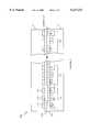
- FIG. 1is a cross-sectional view of a portion of a prior art OLED display.
- FIG. 2is a cross-sectional view of a portion of an OLED display according to the present invention.
- FIG. 1is a cross-sectional view of a portion of a prior art OLED display 10 based on the color conversion methodology.
- Display 10is constructed on a glass substrate 12.
- the light that is converted to the primary colorsis generated in an EL layer 18.
- the light in EL layer 18is generated by connecting row and column electrodes to the appropriate power supplies.
- the row electrodeswill be assumed to be the anode of the device, and the column electrodes will be assumed to be the cathode.
- the cross-sectional view shown in FIG. 1is taken through one row electrode.
- the column electrodesrun at right angles to the row electrodes. Typical column electrodes are shown at 31-33.
- Strip 21converts the light emitted by layer 18 to blue light that escapes through the transparent glass substrate.
- strip 22converts light to green
- strip 23converts the emitted light to red.
- the portion of the display shown in FIG. 1includes the column electrodes for three full color pixels shown at 13-15.
- the minimum distance between the color conversion strips and the light generation layer 18is determined by the thickness of the planarization layer 16. As pointed out above, the difference in thickness between the red conversion strip and the other conversion strips dictates a minimum thickness for the planarization layer. In addition, additional thickness requirements are set by the material and planarization process. Hence, these prior art devices may suffer from off-axis color anomalies. In addition, the planarization process increases the cost of the devices, and the rigid glass substrates prevent the devices from flexing, as well as increasing the cost compared to fabrication on flexible substrates, which allow roll-to-roll processing.
- FIG. 2is a cross-sectional view of a OLED display 100 according to the present invention.
- FIG. 2is also a cross-sectional view through one anode row electrode, anode 117.
- Exemplary cathode electrodesare shown at 131-133. The cathode electrodes run as strips of conducting material in a direction perpendicular to the anode electrodes.
- the anode electrodesare constructed from patterned ITO deposited on a thin plastic sheet 161 which is typically 125 microns or less in thickness, and may be 25 microns or less.
- the preferred material for sheet 161is poly (ethylene terephthalate), which is commonly called polyester, poly (ethylene naphthalate), or transparent polyimide. Other transparent polymers with good thermal and mechanical stability can also be used.
- the various polymer layers that make up the light emitting and injection layersare deposited over the patterned anode electrodes. To simplify the drawing, these layers are shown as a single light emitting layer 118; however, it is to be understood that layer 118 may be constructed of a number of sub-layers that facilitate the injection of holes and electrons into an EL layer as described above. Since the fabrication of such a multilayer structure is conventional in the art, it will not be discussed in detail here. It is sufficient to note that the layers can be deposited by spin casting, dye sublimation, web coating, or various "printing" techniques depending on the particular material system chosen.
- the cathode linesare constructed from a low work-function material such as calcium or magnesium. Shadow masking techniques for depositing such electrodes are also well known in the art, and hence, will not be discussed in detail here.
- the color conversion strips corresponding to the cathode electrodesare deposited on the opposite side of substrate 161 from the light emitting portion of the OLED.
- the color conversion strips corresponding to three pixelsare shown at 113-115.
- the color conversion strips corresponding to cathode electrodes 131-133are shown at 121-123, respectively. It should be noted that the distance between the light emitting area at the intersection of the anode and cathode electrodes and the color conversion strips is now determined solely by the thickness of plastic sheet 161. Hence, color anomalies resulting from the difference in thickness of the color conversion strips are eliminated.
- the thickness of the plastic sheetcan be set to be less than the thickness of the corresponding planarized layer utilized in prior art devices, since transparent plastic substrates with thicknesses of between about 25 and 125 microns are common and easily processed, and thicknesses of less than 25 microns are possible with polyimide-based materials. Accordingly, the present invention can provide improved off-axis performance with respect to color anomalies. In addition, the need for a planarization layer is eliminated.
- devices fabricated on flexible substratescan be constructed on web processing equipment using roll to roll processing techniques that substantially reduce the cost of fabrication relative to techniques based on rigid glass substrates. This advantage is available regardless of whether the fabrication is based on vapor deposition, sublimation, liquid coating or printing techniques. It should also be noted that considerable savings can be realized even if some of the processing steps cannot be performed on roll to roll equipment. For example, the ITO deposition followed by the deposition of the light emitting layer 118 might be carried out on roll to roll equipment even if the deposition of the cathode and/ or color conversion strips were not.
- the color conversion materialscan be applied directly to substrate 161 by any of the techniques described above. Alternatively, these materials may be applied to a separate substrate, and the two substrates laminated together with the color conversion layer adjacent to the substrate 161. This is especially convenient if, for example, the color pattern is to be produced by an inkjet printer or similar device. In this case, the color conversion materials can be jet printed on a conventional overhead projector transparency film.
- the final displaysneed to be encapsulated to prevent oxygen and moisture from penetrating to the cathode electrodes and the light emitting layers.
- Such encapsulation layersare shown at 171 and 172 in FIG. 2.
- the devicemay be encapsulated by sealing it against a transparent glass substrate having the desired curvature using a transparent bonding material.
- the back surface of the devicei.e., the surface containing the cathode electrodes, can be sealed using any barrier material that does not short the cathode electrodes. If the device is to remain flexible, then a flexible sealant can be applied to both sides of the device.
- Displays in which an image is generated that does not depend on x-y addressable pixelsmay also be constructed using the present invention.
- fixed imagescan be generated at different places on the display by utilizing a planar anode and patterning a portion of the cathode and the corresponding portion of the color conversion layer to match the image.
- a voltage applied to that portion of the cathodewill then cause the desired image to "light up" on the display.
- a plurality of such sub-imagescan be incorporated in a display to form a display panel in which one or more messages or images are illuminated in response to the receipt of a predetermined signal.
- the panelcan be quickly, and economically, constructed from a blank panel in which the color conversion layers have not been deposited.
- Such materialcan be provided as a roll that is ready for cutting and patterning for the specific display.
- the cathode of the preformed sheetis patterned with narrow cuts so as to isolate the desired light areas from the dark areas; this may be economically accomplished by, for example, removing material with a solid state laser.
- a separate sheet of plasticis then printed with a metallic image of the cathode pattern. Any metal will suffice; gold would be preferred for its inertness, ductility and ease of printing by electrodeposition or from organometallic inks that are well known in the art of printing.
- the various separate regionsare connected together by printed interconnect metal, and this metal is covered by an insulating polymer (using, for example, an inkjet printer mechanism).
- This sheetis laminated against the cathode to provide the electrical contact. Finally, the color conversion materials are printed on the front of the substrate, as already described. The same method can be used to fabricate a display having a plurality of spatially separate images in which the images are displayed at different times.
Landscapes
- Electroluminescent Light Sources (AREA)
Abstract
Description
Claims (9)
Priority Applications (1)
| Application Number | Priority Date | Filing Date | Title |
|---|---|---|---|
| US09/111,474US6137221A (en) | 1998-07-08 | 1998-07-08 | Organic electroluminescent device with full color characteristics |
Applications Claiming Priority (1)
| Application Number | Priority Date | Filing Date | Title |
|---|---|---|---|
| US09/111,474US6137221A (en) | 1998-07-08 | 1998-07-08 | Organic electroluminescent device with full color characteristics |
Publications (1)
| Publication Number | Publication Date |
|---|---|
| US6137221Atrue US6137221A (en) | 2000-10-24 |
Family
ID=22338760
Family Applications (1)
| Application Number | Title | Priority Date | Filing Date |
|---|---|---|---|
| US09/111,474Expired - LifetimeUS6137221A (en) | 1998-07-08 | 1998-07-08 | Organic electroluminescent device with full color characteristics |
Country Status (1)
| Country | Link |
|---|---|
| US (1) | US6137221A (en) |
Cited By (65)
| Publication number | Priority date | Publication date | Assignee | Title |
|---|---|---|---|---|
| US20010042329A1 (en)* | 2000-04-13 | 2001-11-22 | Matthew Murasko | Electroluminescent sign |
| US20020011786A1 (en)* | 1997-08-04 | 2002-01-31 | Matthew Murasko | Electroluminescent sign |
| US20020074547A1 (en)* | 1996-05-15 | 2002-06-20 | Seiko Epson Corporation | Thin film device provided with coating film, liquid crystal panel and electronic device, and method for making the thin film device |
| US6424093B1 (en)* | 2000-10-06 | 2002-07-23 | Eastman Kodak Company | Organic electroluminescent display device with performed images |
| US6436222B1 (en)* | 2000-05-12 | 2002-08-20 | Eastman Kodak Company | Forming preformed images in organic electroluminescent devices |
| US20020155214A1 (en)* | 2001-03-22 | 2002-10-24 | Matthew Murasko | Illuminated display system and process |
| US20020159246A1 (en)* | 2001-03-21 | 2002-10-31 | Matthew Murasko | Illuminated display system |
| US20020159245A1 (en)* | 2001-03-22 | 2002-10-31 | Matthew Murasko | Integrated illumination system |
| GB2377809A (en)* | 2001-05-31 | 2003-01-22 | Hewlett Packard Co | Flexible electronic device |
| US20030015962A1 (en)* | 2001-06-27 | 2003-01-23 | Matthew Murasko | Electroluminescent panel having controllable transparency |
| US6552364B2 (en)* | 2001-06-22 | 2003-04-22 | International Business Machines Corporation | Organic light emitting devices |
| US20030209973A1 (en)* | 1999-09-03 | 2003-11-13 | 3M Innovative Properties Company | Large area organic electronic devices having conducting polymer buffer layers and methods of making same |
| US6680724B2 (en) | 2001-05-31 | 2004-01-20 | Hewlett-Packard Development Company, L.P. | Flexible electronic viewing device |
| US6773644B1 (en) | 2001-08-29 | 2004-08-10 | Nokia Corporation | Method of making illuminated covers |
| US20040164668A1 (en)* | 2003-02-20 | 2004-08-26 | Hiroshi Kanno | Color light emitting display device |
| US20040206953A1 (en)* | 2003-04-16 | 2004-10-21 | Robert Morena | Hermetically sealed glass package and method of fabrication |
| US20040207314A1 (en)* | 2003-04-16 | 2004-10-21 | Aitken Bruce G. | Glass package that is hermetically sealed with a frit and method of fabrication |
| US6816083B2 (en) | 2002-02-04 | 2004-11-09 | Nokia Corporation | Electronic device with cover including a radio frequency indentification module |
| US6821553B2 (en) | 1996-11-25 | 2004-11-23 | Seiko Epson Corporation | Method of manufacturing organic EL element, organic EL element, and organic EL display device |
| US20050095736A1 (en)* | 2003-11-04 | 2005-05-05 | Raghunath Padiyath | Method of making an organic light emitting device |
| US20050094394A1 (en)* | 2003-11-04 | 2005-05-05 | 3M Innovative Properties Company | Segmented organic light emitting device |
| US20050100660A1 (en)* | 2002-09-19 | 2005-05-12 | Nobuyuki Ito | Method and apparatus for manufacturing organic EL display and color filter by ink jet method |
| US20050104516A1 (en)* | 2003-11-14 | 2005-05-19 | Park Jin-Woo | Super-thin OLED and method for manufacturing the same |
| US20050140282A1 (en)* | 2003-12-30 | 2005-06-30 | Lg.Philips Lcd Co., Ltd. | Organic electroluminescent display device and method of fabricating the same |
| US20050151151A1 (en)* | 2003-04-16 | 2005-07-14 | Hawtof Daniel W. | Hermetically sealed package and method of fabrication of a hermetically sealed package |
| US20060210704A1 (en)* | 1996-09-19 | 2006-09-21 | Seiko Epson Corporation | Method of manufacturing a display device |
| US20060284533A1 (en)* | 2005-06-21 | 2006-12-21 | Au Optronics Corp. | Organic electroluminescent device |
| US20070128967A1 (en)* | 2005-12-06 | 2007-06-07 | Becken Keith J | Method of making a glass envelope |
| US20070128966A1 (en)* | 2005-12-06 | 2007-06-07 | Becken Keith J | Method of encapsulating a display element |
| US20070146915A1 (en)* | 2005-12-28 | 2007-06-28 | Yang Seung G | Color filter array and organic light-emitting display device using the same |
| US20070164376A1 (en)* | 1999-10-25 | 2007-07-19 | Burrows Paul E | Method for edge sealing barrier films |
| US20080124558A1 (en)* | 2006-08-18 | 2008-05-29 | Heather Debra Boek | Boro-silicate glass frits for hermetic sealing of light emitting device displays |
| US20080136317A1 (en)* | 2006-12-06 | 2008-06-12 | General Electric Company | Illumination source providing enhanced color mixing |
| USRE40531E1 (en) | 1999-10-25 | 2008-10-07 | Battelle Memorial Institute | Ultrabarrier substrates |
| USD580377S1 (en)* | 2007-02-09 | 2008-11-11 | Panasonic Corporation | Light source of light-emitting diode |
| USD580889S1 (en)* | 2007-02-09 | 2008-11-18 | Panasonic Corporation | Light source of light-emitting diode |
| USD580890S1 (en)* | 2007-02-09 | 2008-11-18 | Panasonic Corporation | Light source of light-emitting diode |
| USD586764S1 (en)* | 2007-02-09 | 2009-02-17 | Panasonic Corporation | Light source of light-emitting diode |
| US7510913B2 (en) | 2003-04-11 | 2009-03-31 | Vitex Systems, Inc. | Method of making an encapsulated plasma sensitive device |
| US20090169722A1 (en)* | 1999-03-30 | 2009-07-02 | Daniel Luch | Substrate and collector grid structures for integrated series connected photovoltaic arrays and process of manufacture of such arrays |
| US7648925B2 (en) | 2003-04-11 | 2010-01-19 | Vitex Systems, Inc. | Multilayer barrier stacks and methods of making multilayer barrier stacks |
| US7767498B2 (en) | 2005-08-25 | 2010-08-03 | Vitex Systems, Inc. | Encapsulated devices and method of making |
| US7898054B2 (en) | 2000-02-04 | 2011-03-01 | Daniel Luch | Substrate structures for integrated series connected photovoltaic arrays and process of manufacture of such arrays |
| US7898053B2 (en) | 2000-02-04 | 2011-03-01 | Daniel Luch | Substrate structures for integrated series connected photovoltaic arrays and process of manufacture of such arrays |
| US8076568B2 (en) | 2006-04-13 | 2011-12-13 | Daniel Luch | Collector grid and interconnect structures for photovoltaic arrays and modules |
| US20110309389A1 (en)* | 2008-07-23 | 2011-12-22 | Gang Yu | Full-color active matrix organic light emitting display with hybrid |
| US8110737B2 (en) | 1999-03-30 | 2012-02-07 | Daniel Luch | Collector grid, electrode structures and interrconnect structures for photovoltaic arrays and methods of manufacture |
| US8138413B2 (en) | 2006-04-13 | 2012-03-20 | Daniel Luch | Collector grid and interconnect structures for photovoltaic arrays and modules |
| US8198203B2 (en) | 2008-10-20 | 2012-06-12 | Corning Incorporated | Antimony-free glass, antimony-free frit and a glass package that is hermetically sealed with the frit |
| US8198696B2 (en) | 2000-02-04 | 2012-06-12 | Daniel Luch | Substrate structures for integrated series connected photovoltaic arrays and process of manufacture of such arrays |
| US8222513B2 (en) | 2006-04-13 | 2012-07-17 | Daniel Luch | Collector grid, electrode structures and interconnect structures for photovoltaic arrays and methods of manufacture |
| US8448468B2 (en) | 2008-06-11 | 2013-05-28 | Corning Incorporated | Mask and method for sealing a glass envelope |
| US8664030B2 (en) | 1999-03-30 | 2014-03-04 | Daniel Luch | Collector grid and interconnect structures for photovoltaic arrays and modules |
| US8729385B2 (en) | 2006-04-13 | 2014-05-20 | Daniel Luch | Collector grid and interconnect structures for photovoltaic arrays and modules |
| US8808457B2 (en) | 2002-04-15 | 2014-08-19 | Samsung Display Co., Ltd. | Apparatus for depositing a multilayer coating on discrete sheets |
| US8822810B2 (en) | 2006-04-13 | 2014-09-02 | Daniel Luch | Collector grid and interconnect structures for photovoltaic arrays and modules |
| US8884155B2 (en) | 2006-04-13 | 2014-11-11 | Daniel Luch | Collector grid and interconnect structures for photovoltaic arrays and modules |
| US8900366B2 (en) | 2002-04-15 | 2014-12-02 | Samsung Display Co., Ltd. | Apparatus for depositing a multilayer coating on discrete sheets |
| US20150014670A1 (en)* | 2012-01-18 | 2015-01-15 | Sumitomo Chemical Company Limited | Electroluminescence from a plurality of electroluminescent zones in a laterally separated arrangement |
| US9006563B2 (en) | 2006-04-13 | 2015-04-14 | Solannex, Inc. | Collector grid and interconnect structures for photovoltaic arrays and modules |
| US9236512B2 (en) | 2006-04-13 | 2016-01-12 | Daniel Luch | Collector grid and interconnect structures for photovoltaic arrays and modules |
| US9755004B2 (en) | 2011-06-28 | 2017-09-05 | Cbrite Inc. | Full-color active matrix organic light emitting display with hybrid structure |
| US9865758B2 (en) | 2006-04-13 | 2018-01-09 | Daniel Luch | Collector grid and interconnect structures for photovoltaic arrays and modules |
| US9918370B2 (en)* | 2004-12-28 | 2018-03-13 | Samsung Display Co., Ltd. | Electroluminescent devices and methods of making electroluminescent devices including an optical spacer |
| US10950821B2 (en) | 2007-01-26 | 2021-03-16 | Samsung Display Co., Ltd. | Method of encapsulating an environmentally sensitive device |
Citations (3)
| Publication number | Priority date | Publication date | Assignee | Title |
|---|---|---|---|---|
| US5126214A (en)* | 1989-03-15 | 1992-06-30 | Idemitsu Kosan Co., Ltd. | Electroluminescent element |
| US5705285A (en)* | 1996-09-03 | 1998-01-06 | Motorola, Inc. | Multicolored organic electroluminescent display |
| US5986400A (en)* | 1994-09-06 | 1999-11-16 | U.S. Philips Corporation | Electroluminescent device comprising a transparent structured electrode layer made from a conductive polymer |
- 1998
- 1998-07-08USUS09/111,474patent/US6137221A/ennot_activeExpired - Lifetime
Patent Citations (3)
| Publication number | Priority date | Publication date | Assignee | Title |
|---|---|---|---|---|
| US5126214A (en)* | 1989-03-15 | 1992-06-30 | Idemitsu Kosan Co., Ltd. | Electroluminescent element |
| US5986400A (en)* | 1994-09-06 | 1999-11-16 | U.S. Philips Corporation | Electroluminescent device comprising a transparent structured electrode layer made from a conductive polymer |
| US5705285A (en)* | 1996-09-03 | 1998-01-06 | Motorola, Inc. | Multicolored organic electroluminescent display |
Cited By (116)
| Publication number | Priority date | Publication date | Assignee | Title |
|---|---|---|---|---|
| US7229859B2 (en) | 1996-05-15 | 2007-06-12 | Seiko Epson Corporation | Thin film device provided with coating film, liquid crystal panel and electronic device, and method for making the thin film device |
| US20030134519A1 (en)* | 1996-05-15 | 2003-07-17 | Seiko Epson Corporation | Thin film device provided with coating film, liquid crystal panel and electronic device, and method for making the thin film device |
| US20020074547A1 (en)* | 1996-05-15 | 2002-06-20 | Seiko Epson Corporation | Thin film device provided with coating film, liquid crystal panel and electronic device, and method for making the thin film device |
| US7067337B2 (en) | 1996-05-15 | 2006-06-27 | Seiko Epson Corporation | Thin film device provided with coating film, liquid crystal panel and electronic device, and method for making the thin film device |
| US8431182B2 (en) | 1996-09-19 | 2013-04-30 | Seiko Epson Corporation | Matrix type display device and manufacturing method thereof |
| US20090053396A1 (en)* | 1996-09-19 | 2009-02-26 | Seiko Epson Corporation | Matrix type display device and manufacturing method thereof |
| US20060210704A1 (en)* | 1996-09-19 | 2006-09-21 | Seiko Epson Corporation | Method of manufacturing a display device |
| US8580333B2 (en) | 1996-09-19 | 2013-11-12 | Seiko Epson Corporation | Matrix type display device with optical material at predetermined positions and manufacturing method thereof |
| US7662425B2 (en) | 1996-11-25 | 2010-02-16 | Seiko Epson Corporation | Method of manufacturing organic EL element, organic EL element and organic EL display device |
| US20100120185A1 (en)* | 1996-11-25 | 2010-05-13 | Seiko Epson Corporation | Method of manufacturing organic el element, organic el element, and organic el display device |
| US6821553B2 (en) | 1996-11-25 | 2004-11-23 | Seiko Epson Corporation | Method of manufacturing organic EL element, organic EL element, and organic EL display device |
| US8614545B2 (en) | 1996-11-25 | 2013-12-24 | Seiko Epson Corporation | Organic EL display device having a bank formed to fill spaces between pixel electrodes |
| US6863961B2 (en) | 1996-11-25 | 2005-03-08 | Seiko Epson Corporation | Method of manufacturing organic EL element, organic EL element, and organic EL display device |
| US6838192B2 (en)* | 1996-11-25 | 2005-01-04 | Seiko Epson Corporation | Method of manufacturing organic EL element, organic EL element, and organic EL display device |
| US20020011786A1 (en)* | 1997-08-04 | 2002-01-31 | Matthew Murasko | Electroluminescent sign |
| US6965196B2 (en) | 1997-08-04 | 2005-11-15 | Lumimove, Inc. | Electroluminescent sign |
| US7989693B2 (en) | 1999-03-30 | 2011-08-02 | Daniel Luch | Substrate and collector grid structures for integrated series connected photovoltaic arrays and process of manufacture of such arrays |
| US7851700B2 (en) | 1999-03-30 | 2010-12-14 | Daniel Luch | Substrate and collector grid structures for integrated series connected photovoltaic arrays and process of manufacture of such arrays |
| US8664030B2 (en) | 1999-03-30 | 2014-03-04 | Daniel Luch | Collector grid and interconnect structures for photovoltaic arrays and modules |
| US20090169722A1 (en)* | 1999-03-30 | 2009-07-02 | Daniel Luch | Substrate and collector grid structures for integrated series connected photovoltaic arrays and process of manufacture of such arrays |
| US8304646B2 (en) | 1999-03-30 | 2012-11-06 | Daniel Luch | Substrate and collector grid structures for integrated series connected photovoltaic arrays and process of manufacture of such arrays |
| US7989692B2 (en) | 1999-03-30 | 2011-08-02 | Daniel Luch | Substrate and collector grid structures for integrated series connected photovoltaic arrays and process of manufacturing of such arrays |
| US8319097B2 (en) | 1999-03-30 | 2012-11-27 | Daniel Luch | Substrate and collector grid structures for integrated series connected photovoltaic arrays and process of manufacture of such arrays |
| US8110737B2 (en) | 1999-03-30 | 2012-02-07 | Daniel Luch | Collector grid, electrode structures and interrconnect structures for photovoltaic arrays and methods of manufacture |
| US20030209973A1 (en)* | 1999-09-03 | 2003-11-13 | 3M Innovative Properties Company | Large area organic electronic devices having conducting polymer buffer layers and methods of making same |
| US7727601B2 (en) | 1999-10-25 | 2010-06-01 | Vitex Systems, Inc. | Method for edge sealing barrier films |
| USRE40531E1 (en) | 1999-10-25 | 2008-10-07 | Battelle Memorial Institute | Ultrabarrier substrates |
| US20070164376A1 (en)* | 1999-10-25 | 2007-07-19 | Burrows Paul E | Method for edge sealing barrier films |
| US7898054B2 (en) | 2000-02-04 | 2011-03-01 | Daniel Luch | Substrate structures for integrated series connected photovoltaic arrays and process of manufacture of such arrays |
| US7898053B2 (en) | 2000-02-04 | 2011-03-01 | Daniel Luch | Substrate structures for integrated series connected photovoltaic arrays and process of manufacture of such arrays |
| US8198696B2 (en) | 2000-02-04 | 2012-06-12 | Daniel Luch | Substrate structures for integrated series connected photovoltaic arrays and process of manufacture of such arrays |
| US20010042329A1 (en)* | 2000-04-13 | 2001-11-22 | Matthew Murasko | Electroluminescent sign |
| US7144289B2 (en) | 2000-04-13 | 2006-12-05 | Lumimove, Inc. | Method of forming an illuminated design on a substrate |
| US20040058615A1 (en)* | 2000-04-13 | 2004-03-25 | Matthew Murasko | Electroluminescent sign |
| US6436222B1 (en)* | 2000-05-12 | 2002-08-20 | Eastman Kodak Company | Forming preformed images in organic electroluminescent devices |
| EP1154398A3 (en)* | 2000-05-12 | 2004-11-03 | Eastman Kodak Company | Forming preformed images in organic electroluminescent devices |
| US6424093B1 (en)* | 2000-10-06 | 2002-07-23 | Eastman Kodak Company | Organic electroluminescent display device with performed images |
| US20020159246A1 (en)* | 2001-03-21 | 2002-10-31 | Matthew Murasko | Illuminated display system |
| US7745018B2 (en) | 2001-03-22 | 2010-06-29 | Lumimove, Inc. | Illuminated display system and process |
| US6811895B2 (en) | 2001-03-22 | 2004-11-02 | Lumimove, Inc. | Illuminated display system and process |
| US7048400B2 (en) | 2001-03-22 | 2006-05-23 | Lumimove, Inc. | Integrated illumination system |
| US20020159245A1 (en)* | 2001-03-22 | 2002-10-31 | Matthew Murasko | Integrated illumination system |
| US20020155214A1 (en)* | 2001-03-22 | 2002-10-24 | Matthew Murasko | Illuminated display system and process |
| US20050061671A1 (en)* | 2001-03-22 | 2005-03-24 | Matthew Murasko | IIluminated display system and process |
| US6680724B2 (en) | 2001-05-31 | 2004-01-20 | Hewlett-Packard Development Company, L.P. | Flexible electronic viewing device |
| GB2377809A (en)* | 2001-05-31 | 2003-01-22 | Hewlett Packard Co | Flexible electronic device |
| US6723591B2 (en) | 2001-06-22 | 2004-04-20 | International Business Machines Corporation | Organic light emitting devices |
| US20030146453A1 (en)* | 2001-06-22 | 2003-08-07 | International Business Machines Corporation | Organic light emitting devices |
| US6552364B2 (en)* | 2001-06-22 | 2003-04-22 | International Business Machines Corporation | Organic light emitting devices |
| US20030015962A1 (en)* | 2001-06-27 | 2003-01-23 | Matthew Murasko | Electroluminescent panel having controllable transparency |
| US6773644B1 (en) | 2001-08-29 | 2004-08-10 | Nokia Corporation | Method of making illuminated covers |
| US6790396B2 (en) | 2001-08-29 | 2004-09-14 | Nokia Corporation | Method of making illuminated covers |
| US6816083B2 (en) | 2002-02-04 | 2004-11-09 | Nokia Corporation | Electronic device with cover including a radio frequency indentification module |
| US8900366B2 (en) | 2002-04-15 | 2014-12-02 | Samsung Display Co., Ltd. | Apparatus for depositing a multilayer coating on discrete sheets |
| US8808457B2 (en) | 2002-04-15 | 2014-08-19 | Samsung Display Co., Ltd. | Apparatus for depositing a multilayer coating on discrete sheets |
| US7368145B2 (en)* | 2002-09-19 | 2008-05-06 | Dai Nippon Printing Co., Ltd. | Method and apparatus for manufacturing organic EL display and color filter by ink jet method |
| US20050100660A1 (en)* | 2002-09-19 | 2005-05-12 | Nobuyuki Ito | Method and apparatus for manufacturing organic EL display and color filter by ink jet method |
| US20040164668A1 (en)* | 2003-02-20 | 2004-08-26 | Hiroshi Kanno | Color light emitting display device |
| US7648925B2 (en) | 2003-04-11 | 2010-01-19 | Vitex Systems, Inc. | Multilayer barrier stacks and methods of making multilayer barrier stacks |
| US7510913B2 (en) | 2003-04-11 | 2009-03-31 | Vitex Systems, Inc. | Method of making an encapsulated plasma sensitive device |
| US7602121B2 (en) | 2003-04-16 | 2009-10-13 | Corning Incorporated | Glass package that is hermetically sealed with a frit and method of fabrication |
| US7344901B2 (en) | 2003-04-16 | 2008-03-18 | Corning Incorporated | Hermetically sealed package and method of fabricating of a hermetically sealed package |
| US20050151151A1 (en)* | 2003-04-16 | 2005-07-14 | Hawtof Daniel W. | Hermetically sealed package and method of fabrication of a hermetically sealed package |
| US7407423B2 (en) | 2003-04-16 | 2008-08-05 | Corning Incorporated | Glass package that is hermetically sealed with a frit and method of fabrication |
| US20040206953A1 (en)* | 2003-04-16 | 2004-10-21 | Robert Morena | Hermetically sealed glass package and method of fabrication |
| US20040207314A1 (en)* | 2003-04-16 | 2004-10-21 | Aitken Bruce G. | Glass package that is hermetically sealed with a frit and method of fabrication |
| US20050001545A1 (en)* | 2003-04-16 | 2005-01-06 | Aitken Bruce G. | Glass package that is hermetically sealed with a frit and method of fabrication |
| US6998776B2 (en) | 2003-04-16 | 2006-02-14 | Corning Incorporated | Glass package that is hermetically sealed with a frit and method of fabrication |
| US20070007894A1 (en)* | 2003-04-16 | 2007-01-11 | Aitken Bruce G | Glass package that is hermetically sealed with a frit and method of fabrication |
| US8063560B2 (en) | 2003-04-16 | 2011-11-22 | Corning Incorporated | Glass package that is hermetically sealed with a frit and method of fabrication |
| US20050095736A1 (en)* | 2003-11-04 | 2005-05-05 | Raghunath Padiyath | Method of making an organic light emitting device |
| US20050094394A1 (en)* | 2003-11-04 | 2005-05-05 | 3M Innovative Properties Company | Segmented organic light emitting device |
| US7432124B2 (en)* | 2003-11-04 | 2008-10-07 | 3M Innovative Properties Company | Method of making an organic light emitting device |
| US7271534B2 (en) | 2003-11-04 | 2007-09-18 | 3M Innovative Properties Company | Segmented organic light emitting device |
| US20080230777A1 (en)* | 2003-11-04 | 2008-09-25 | 3M Innovative Properties Company | Method of making an organic light emitting device |
| US7858976B2 (en)* | 2003-11-04 | 2010-12-28 | 3M Innovative Properties Company | Method of making an organic light emitting device |
| US20050104516A1 (en)* | 2003-11-14 | 2005-05-19 | Park Jin-Woo | Super-thin OLED and method for manufacturing the same |
| US7828618B2 (en) | 2003-11-14 | 2010-11-09 | Samsung Mobile Display Co., Ltd. | Super-thin OLED and method for manufacturing the same |
| US20050140282A1 (en)* | 2003-12-30 | 2005-06-30 | Lg.Philips Lcd Co., Ltd. | Organic electroluminescent display device and method of fabricating the same |
| US7649311B2 (en)* | 2003-12-30 | 2010-01-19 | Lg Display Co., Ltd. | Organic electroluminescent display device and method of fabricating the same |
| US9918370B2 (en)* | 2004-12-28 | 2018-03-13 | Samsung Display Co., Ltd. | Electroluminescent devices and methods of making electroluminescent devices including an optical spacer |
| US20060284533A1 (en)* | 2005-06-21 | 2006-12-21 | Au Optronics Corp. | Organic electroluminescent device |
| US7812359B2 (en) | 2005-06-21 | 2010-10-12 | Au Optronics Corp. | Organic electroluminescent device |
| US7767498B2 (en) | 2005-08-25 | 2010-08-03 | Vitex Systems, Inc. | Encapsulated devices and method of making |
| US20070128967A1 (en)* | 2005-12-06 | 2007-06-07 | Becken Keith J | Method of making a glass envelope |
| US20070128966A1 (en)* | 2005-12-06 | 2007-06-07 | Becken Keith J | Method of encapsulating a display element |
| US7597603B2 (en) | 2005-12-06 | 2009-10-06 | Corning Incorporated | Method of encapsulating a display element |
| US7537504B2 (en) | 2005-12-06 | 2009-05-26 | Corning Incorporated | Method of encapsulating a display element with frit wall and laser beam |
| US20070146915A1 (en)* | 2005-12-28 | 2007-06-28 | Yang Seung G | Color filter array and organic light-emitting display device using the same |
| US8409727B2 (en)* | 2005-12-28 | 2013-04-02 | Samsung Display Co., Ltd. | Color filter array and organic light-emitting display device using the same |
| US8138413B2 (en) | 2006-04-13 | 2012-03-20 | Daniel Luch | Collector grid and interconnect structures for photovoltaic arrays and modules |
| US8222513B2 (en) | 2006-04-13 | 2012-07-17 | Daniel Luch | Collector grid, electrode structures and interconnect structures for photovoltaic arrays and methods of manufacture |
| US8076568B2 (en) | 2006-04-13 | 2011-12-13 | Daniel Luch | Collector grid and interconnect structures for photovoltaic arrays and modules |
| US9865758B2 (en) | 2006-04-13 | 2018-01-09 | Daniel Luch | Collector grid and interconnect structures for photovoltaic arrays and modules |
| US9236512B2 (en) | 2006-04-13 | 2016-01-12 | Daniel Luch | Collector grid and interconnect structures for photovoltaic arrays and modules |
| US9006563B2 (en) | 2006-04-13 | 2015-04-14 | Solannex, Inc. | Collector grid and interconnect structures for photovoltaic arrays and modules |
| US8884155B2 (en) | 2006-04-13 | 2014-11-11 | Daniel Luch | Collector grid and interconnect structures for photovoltaic arrays and modules |
| US8729385B2 (en) | 2006-04-13 | 2014-05-20 | Daniel Luch | Collector grid and interconnect structures for photovoltaic arrays and modules |
| US8822810B2 (en) | 2006-04-13 | 2014-09-02 | Daniel Luch | Collector grid and interconnect structures for photovoltaic arrays and modules |
| US20080124558A1 (en)* | 2006-08-18 | 2008-05-29 | Heather Debra Boek | Boro-silicate glass frits for hermetic sealing of light emitting device displays |
| US7728514B2 (en)* | 2006-12-06 | 2010-06-01 | General Electric Company | Illumination source providing enhanced color mixing |
| US20080136317A1 (en)* | 2006-12-06 | 2008-06-12 | General Electric Company | Illumination source providing enhanced color mixing |
| US10950821B2 (en) | 2007-01-26 | 2021-03-16 | Samsung Display Co., Ltd. | Method of encapsulating an environmentally sensitive device |
| USD580377S1 (en)* | 2007-02-09 | 2008-11-11 | Panasonic Corporation | Light source of light-emitting diode |
| USD580889S1 (en)* | 2007-02-09 | 2008-11-18 | Panasonic Corporation | Light source of light-emitting diode |
| USD580890S1 (en)* | 2007-02-09 | 2008-11-18 | Panasonic Corporation | Light source of light-emitting diode |
| USD586764S1 (en)* | 2007-02-09 | 2009-02-17 | Panasonic Corporation | Light source of light-emitting diode |
| US8448468B2 (en) | 2008-06-11 | 2013-05-28 | Corning Incorporated | Mask and method for sealing a glass envelope |
| US9399594B2 (en) | 2008-06-11 | 2016-07-26 | Corning Incorporated | Mask and method for sealing a glass envelope |
| US8742658B2 (en)* | 2008-07-23 | 2014-06-03 | Cbrite Inc. | Full-color active matrix organic light emitting display with hybrid |
| US20110309389A1 (en)* | 2008-07-23 | 2011-12-22 | Gang Yu | Full-color active matrix organic light emitting display with hybrid |
| US8434328B2 (en) | 2008-10-20 | 2013-05-07 | Corning Incorporated | Antimony-free glass, antimony-free frit and a glass package that is hermetically sealed with the frit |
| US8198203B2 (en) | 2008-10-20 | 2012-06-12 | Corning Incorporated | Antimony-free glass, antimony-free frit and a glass package that is hermetically sealed with the frit |
| US9755004B2 (en) | 2011-06-28 | 2017-09-05 | Cbrite Inc. | Full-color active matrix organic light emitting display with hybrid structure |
| US20150014670A1 (en)* | 2012-01-18 | 2015-01-15 | Sumitomo Chemical Company Limited | Electroluminescence from a plurality of electroluminescent zones in a laterally separated arrangement |
| US9299938B2 (en)* | 2012-01-18 | 2016-03-29 | Sumitomo Chemical Company Limited | Electroluminescence from a plurality of electroluminescent zones in a laterally separated arrangement |
Similar Documents
| Publication | Publication Date | Title |
|---|---|---|
| US6137221A (en) | Organic electroluminescent device with full color characteristics | |
| KR100670543B1 (en) | Organic electroluminescent device | |
| US6388377B1 (en) | Electroluminescent element with banks intersecting anode group | |
| US6936856B2 (en) | Multi substrate organic light emitting devices | |
| JP5808624B2 (en) | Display device and electronic device | |
| US8872200B2 (en) | Display device and electronic apparatus | |
| US7034452B2 (en) | Dual-type organic electroluminescence display and manufacturing method thereof | |
| US7405514B2 (en) | Organic EL display device with plural electrode segments | |
| WO2003026012A2 (en) | Organic light emitting diode light source | |
| US7642109B2 (en) | Electrical connection in OLED devices | |
| US8674598B2 (en) | Polychromatic electronic display device with electroluminescent screen | |
| KR20090087274A (en) | OLED display and manufacturing method thereof | |
| CN102208432B (en) | Transmission type colored organic EL (Electro-Luminescence) display device | |
| US11803263B2 (en) | Display panel and display device | |
| US7221094B2 (en) | Electroluminescent device and method of manufacturing the same | |
| US6388387B1 (en) | Optical element | |
| US7837822B2 (en) | Laser induced thermal imaging apparatus and method of fabricating organic light emitting display using the same | |
| US7473924B2 (en) | Electroluminescent device with a blocking layer and a dummy electrode region | |
| KR100581775B1 (en) | Organic electroluminescent device and manufacturing method thereof | |
| KR20050050572A (en) | Electroluminescent element and lighting unit | |
| JPH11135257A (en) | Method for manufacturing organic electroluminescence device | |
| CN109768074B (en) | Display substrate, manufacturing method thereof, display panel and display device | |
| US6078138A (en) | Organic thin film electroluminescence display unit | |
| CN113013215A (en) | Display panel, display device and preparation method | |
| EP0966018A1 (en) | Light-emissive devices |
Legal Events
| Date | Code | Title | Description |
|---|---|---|---|
| AS | Assignment | Owner name:HEWLETT-PACKARD COMPANY, CALIFORNIA Free format text:ASSIGNMENT OF ASSIGNORS INTEREST;ASSIGNORS:ROITMAN, DANIEL B.;SHEATS, JAMES R.;REEL/FRAME:009384/0240 Effective date:19980708 | |
| AS | Assignment | Owner name:HEWLETT-PACKARD COMPANY, COLORADO Free format text:MERGER;ASSIGNOR:HEWLETT-PACKARD COMPANY;REEL/FRAME:010759/0049 Effective date:19980520 | |
| AS | Assignment | Owner name:AGILENT TECHNOLOGIES INC, CALIFORNIA Free format text:ASSIGNMENT OF ASSIGNORS INTEREST;ASSIGNOR:HEWLETT-PACKARD COMPANY;REEL/FRAME:010977/0540 Effective date:19991101 | |
| STCF | Information on status: patent grant | Free format text:PATENTED CASE | |
| FEPP | Fee payment procedure | Free format text:PAYOR NUMBER ASSIGNED (ORIGINAL EVENT CODE: ASPN); ENTITY STATUS OF PATENT OWNER: LARGE ENTITY | |
| FPAY | Fee payment | Year of fee payment:4 | |
| AS | Assignment | Owner name:AVAGO TECHNOLOGIES GENERAL IP PTE. LTD., SINGAPORE Free format text:ASSIGNMENT OF ASSIGNORS INTEREST;ASSIGNOR:AGILENT TECHNOLOGIES, INC.;REEL/FRAME:017207/0020 Effective date:20051201 | |
| AS | Assignment | Owner name:AVAGO TECHNOLOGIES ECBU IP (SINGAPORE) PTE. LTD., SINGAPORE Free format text:ASSIGNMENT OF ASSIGNORS INTEREST;ASSIGNOR:AVAGO TECHNOLOGIES GENERAL IP (SINGAPORE) PTE. LTD.;REEL/FRAME:017675/0518 Effective date:20060127 Owner name:AVAGO TECHNOLOGIES ECBU IP (SINGAPORE) PTE. LTD.,S Free format text:ASSIGNMENT OF ASSIGNORS INTEREST;ASSIGNOR:AVAGO TECHNOLOGIES GENERAL IP (SINGAPORE) PTE. LTD.;REEL/FRAME:017675/0518 Effective date:20060127 Owner name:AVAGO TECHNOLOGIES ECBU IP (SINGAPORE) PTE. LTD., Free format text:ASSIGNMENT OF ASSIGNORS INTEREST;ASSIGNOR:AVAGO TECHNOLOGIES GENERAL IP (SINGAPORE) PTE. LTD.;REEL/FRAME:017675/0518 Effective date:20060127 | |
| FPAY | Fee payment | Year of fee payment:8 | |
| AS | Assignment | Owner name:CHIMEI INNOLUX CORPORATION, TAIWAN Free format text:ASSIGNMENT OF ASSIGNORS INTEREST;ASSIGNORS:AVAGO TECHNOLOGIES GENERAL IP (SINGAPORE) PTE. LTD.;AVAGO TECHNOLOGIES ECBU IP (SINGAPORE) PTD. LTD.;AVAGO TECHNOLOGIES FIBER IP (SINGAPORE) PTE. LTD.;REEL/FRAME:027536/0215 Effective date:20110928 | |
| AS | Assignment | Owner name:CHIMEI INNOLUX CORPORATION, TAIWAN Free format text:CORRECTIVE ASSIGNMENT TO CORRECT THE SECOND ASSIGNEE NAME FROM AVAGO TECHNOLOGIES ECBU IP (SINGAPORE) PTD. LTD. TO AVAGO TECHNOLOGIES ECBU IP (SINGAPORE) PTE. LTD. PREVIOUSLY RECORDED ON REEL 027536 FRAME 0215. ASSIGNOR(S) HEREBY CONFIRMS THE ASSIGNMENT TO CHIMEI INNOLUX CORPORATION;ASSIGNORS:AVAGO TECHNOLOGIES GENERAL IP (SINGAPORE) PTE. LTD.;AVAGO TECHNOLOGIES ECBU IP (SINGAPORE) PTE. LTD.;AVAGO TECHNOLOGIES FIBER IP (SINGAPORE) PTE. LTD.;REEL/FRAME:027617/0727 Effective date:20110928 | |
| FPAY | Fee payment | Year of fee payment:12 | |
| AS | Assignment | Owner name:INNOLUX CORPORATION, TAIWAN Free format text:CHANGE OF NAME;ASSIGNOR:CHIMEI INNOLUX CORPORATION;REEL/FRAME:032589/0585 Effective date:20121219 | |
| AS | Assignment | Owner name:AVAGO TECHNOLOGIES GENERAL IP (SINGAPORE) PTE. LTD Free format text:CORRECTIVE ASSIGNMENT TO CORRECT THE NAME OF THE ASSIGNEE PREVIOUSLY RECORDED ON REEL 017207 FRAME 0020. ASSIGNOR(S) HEREBY CONFIRMS THE ASSIGNMENT;ASSIGNOR:AGILENT TECHNOLOGIES, INC.;REEL/FRAME:038633/0001 Effective date:20051201 |