US6137167A - Multichip module with built in repeaters and method - Google Patents
Multichip module with built in repeaters and methodDownload PDFInfo
- Publication number
- US6137167A US6137167AUS09/199,704US19970498AUS6137167AUS 6137167 AUS6137167 AUS 6137167AUS 19970498 AUS19970498 AUS 19970498AUS 6137167 AUS6137167 AUS 6137167A
- Authority
- US
- United States
- Prior art keywords
- interposer
- interconnections
- coupled
- module
- repeater
- Prior art date
- Legal status (The legal status is an assumption and is not a legal conclusion. Google has not performed a legal analysis and makes no representation as to the accuracy of the status listed.)
- Expired - Lifetime
Links
Images


Classifications
- H—ELECTRICITY
- H01—ELECTRIC ELEMENTS
- H01L—SEMICONDUCTOR DEVICES NOT COVERED BY CLASS H10
- H01L25/00—Assemblies consisting of a plurality of semiconductor or other solid state devices
- H01L25/18—Assemblies consisting of a plurality of semiconductor or other solid state devices the devices being of the types provided for in two or more different main groups of the same subclass of H10B, H10D, H10F, H10H, H10K or H10N
- H—ELECTRICITY
- H01—ELECTRIC ELEMENTS
- H01L—SEMICONDUCTOR DEVICES NOT COVERED BY CLASS H10
- H01L25/00—Assemblies consisting of a plurality of semiconductor or other solid state devices
- H01L25/03—Assemblies consisting of a plurality of semiconductor or other solid state devices all the devices being of a type provided for in a single subclass of subclasses H10B, H10D, H10F, H10H, H10K or H10N, e.g. assemblies of rectifier diodes
- H01L25/04—Assemblies consisting of a plurality of semiconductor or other solid state devices all the devices being of a type provided for in a single subclass of subclasses H10B, H10D, H10F, H10H, H10K or H10N, e.g. assemblies of rectifier diodes the devices not having separate containers
- H01L25/065—Assemblies consisting of a plurality of semiconductor or other solid state devices all the devices being of a type provided for in a single subclass of subclasses H10B, H10D, H10F, H10H, H10K or H10N, e.g. assemblies of rectifier diodes the devices not having separate containers the devices being of a type provided for in group H10D89/00
- H01L25/0652—Assemblies consisting of a plurality of semiconductor or other solid state devices all the devices being of a type provided for in a single subclass of subclasses H10B, H10D, H10F, H10H, H10K or H10N, e.g. assemblies of rectifier diodes the devices not having separate containers the devices being of a type provided for in group H10D89/00 the devices being arranged next and on each other, i.e. mixed assemblies
- H—ELECTRICITY
- H01—ELECTRIC ELEMENTS
- H01L—SEMICONDUCTOR DEVICES NOT COVERED BY CLASS H10
- H01L2924/00—Indexing scheme for arrangements or methods for connecting or disconnecting semiconductor or solid-state bodies as covered by H01L24/00
- H01L2924/0001—Technical content checked by a classifier
- H01L2924/0002—Not covered by any one of groups H01L24/00, H01L24/00 and H01L2224/00
- H—ELECTRICITY
- H01—ELECTRIC ELEMENTS
- H01L—SEMICONDUCTOR DEVICES NOT COVERED BY CLASS H10
- H01L2924/00—Indexing scheme for arrangements or methods for connecting or disconnecting semiconductor or solid-state bodies as covered by H01L24/00
- H01L2924/30—Technical effects
- H01L2924/301—Electrical effects
- H01L2924/3011—Impedance
Definitions
- This inventionrelates generally to multichip modules and more particularly to multichip modules using interposers formed from semiconductor material.
- MCMmultichip module
- thermal coefficient of expansion mismatch between the die and the interposerbecomes increasingly critical, at least in part because the thickness of the material forming the die is not increased as the area of the die is increased.
- One solution to this problemis to make the interposer from the same material that the die are made from, i.e., silicon. This allows increasingly complex integrated circuits to be interconnected without exaggerating thermal coefficient of expansion mismatch problems that could occur either during packaging or as a result of thermal cycling in normal use.
- passive componentsmay be formed or mounted on the interposer, as described in "High Frequency IC to IC Signaling on Rapidly Prototyped Flip Chip MCM-D Substrate", by J. Reed et al., 1998 Int. Conf. on MCMs and High Density Packaging, IEEE Cat. No. 0-7803-4850-8/98, pp. 172-177.
- Integrated Passive Components in MCM-Si Technology and their Applications in RF-Systemsby J. Hartung, 1998 Int. Conf. on MCMs and High Density Packaging, pp. 256-261, IEEE Cat. No. 0-7803-4850-8/98, describes an approach whereby multiple aluminum layers are conventionally formed and patterned on the silicon interposer to provide interconnections.
- the aluminum layersare separated by conventional Si 3 N 4 interlevel dielectric layers, allowing capacitors to be formed on the silicon interposer.
- a TaSi layeris formed and patterned on the silicon interposer to provide resistors.
- the present inventionincludes a method for coupling signals between a plurality of integrated circuits mounted on an interposer.
- the methodincludes coupling signals from a first integrated circuit mounted on the interposer to one segment of an interconnection formed on the interposer, propagating the signals for one distance along the one segment and detecting the signals by a repeater circuit coupled to the interposer.
- the methodalso includes regenerating the signals by the repeater circuit and coupling the regenerated signals to another segment of the interconnection, allowing the regenerated signals to be coupled to another of the integrated circuits.
- the present inventionincludes an interposer having utility in multichip modules.
- the interposerincludes a wafer of semiconductor material and a plurality of interconnections formed on a surface of the wafer.
- One or more repeater circuitsare disposed on the wafer and are electrically coupled to lengths of one or more of the plurality of interconnections.
- multiple integrated circuit dieare mounted on the interposer and are electrically interconnected by the interconnections and the repeater circuits.
- the integrated circuitsmay include microprocessors, memory integrated circuits such as DRAMs or SRAMs or specialized I/O integrated circuits.
- Passive componentsmay be formed on or mounted on the interposer.
- the repeater circuitsmodify quadratic RC transmission delays experienced by signals coupled across the interposer in the interconnections. Crosstalk between interconnections and power dissipation are reduced by proper placement of the repeater circuits and the interconnections on the interposer.
- the repeater circuitsmay be formed monolithically in the interposer or may be separate integrated circuits that are coupled to the interposer.
- the integrated circuits, the interconnections and the repeater circuitsare enclosed by a lid.
- contents of the multichip moduleare protected from mechanical and chemical attack.
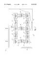
- FIG. 1is a simplified plan view of a multichip module, in accordance with an embodiment of the present invention.
- FIG. 2is a simplified cross-sectional view, taken along section lines II--II of FIG. 1, of an embodiment of a multichip module, in accordance with an embodiment of the present invention.
- FIG. 3is a simplified cross-sectional view, taken along section lines II--II of FIG. 1, of an embodiment of a multichip module, in accordance with an embodiment of the present invention.
- FIG. 4is a simplified schematic diagram of a CMOS repeater circuit, in accordance with an embodiment of the present invention.
- FIG. 5is a simplified schematic diagram of a driver circuit employing reduced output voltage swing, in accordance with an embodiment of the present invention.
- FIG. 6is a simplified schematic diagram of a repeater circuit employing reduced input and output voltage swing, in accordance with an embodiment of the present invention.
- FIG. 7is a simplified schematic diagram of a receiver circuit employing reduced input voltage swing, in accordance with an embodiment of the present invention.
- FIG. 1is a simplified plan view of a multichip module 10, in accordance with an embodiment of the present invention.
- the MCM 10includes interconnections 12 formed on surface portions of an interposer 14.
- the interposer 14is formed from silicon.
- Integrated circuits 16are physically secured and electrically connected to the interposer 14 by any suitable conventional technology.
- the integrated circuits 16may include DRAM or SRAM memories, microprocessors, controllers, microcontrollers, power conditioning circuits, sensor circuits, interfacing and communications circuits, or any other type of known or future developed circuits.
- repeater circuits 18are also coupled to the interposer 14.
- the repeater circuits 18detect signals transmitted from one of the integrated circuits 16, correct slew rate degradation of transitions in these signals and also correct signal amplitude degradation to provide regenerated signals.
- the regenerated signalsare then retransmitted by the repeater circuits 18 to either another of the repeater circuits 18 or to another one of the integrated circuits 16 that is the intended destination of the signals.
- the quadratic signal delay associated with long interconnections 12 having RC transmission line characteristicsis converted to a linear signal propagation delay.
- the interposer 14also includes a region 20 for attachment of a package lid 22, shown in a partial cutaway view in FIG. 1.
- the package lid 22may be a metal lid 22 that is attached to a metallized region 20 by welding or a ceramic lid 22 that is attached to a region 20 coated with a low temperature glass frit by firing the frit in an oven.
- the lid 22 and the interposer 14then form a complete package surrounding the integrated circuits 16, the interconnections 12 and the repeater circuits 18.
- the packagethen protects the "guts" of the MCM 10 from damage that otherwise could result from mechanical abrasion, puncture or chipping, chemical attack and other environmental insults.
- the passive component 24may be a high value capacitor, such as a tantalum or electrolytic capacitor for power conditioning, or may be a sensor, such as a Hall effect sensor, accelerometer (e.g., employing a piezoresistive membrane coupled to a motion-sensing mass), thermistor or thermocouple, optical sensor or transmitter (e.g., photodiode, laser, LED or the like) or may be a frequency selection component such as a SAW or crystal, or may be any other known or future developed circuit component. Capabilities for interconnecting components 24 that achieve functions not generally possible for the integrated circuits 12 can result in increased performance for the MCM 10.
- a sensorsuch as a Hall effect sensor, accelerometer (e.g., employing a piezoresistive membrane coupled to a motion-sensing mass), thermistor or thermocouple, optical sensor or transmitter (e.g., photodiode, laser, LED or the like) or may be a frequency selection component such as a SAW or
- FIG. 2is a simplified cross-sectional view, taken along section lines II--II of FIG. 1, of an embodiment of a MCM 30, in accordance with some embodiments of the present invention.
- Many of the components used in the embodiment of the MCM 30 of FIG. 2are identical to components used in the embodiment of the MCM 10 of FIG. 1. Therefore, in the interest of brevity, these components have been provided with the same reference numerals, and an explanation of them will not be repeated.
- one or more insulating layers 32 formed on a surface of the interposer 14insulate at least portions of an optional resistive layer 34 and the interconnections 12. It will be appreciated that while four insulating layers 32, one resistive layer 34 and two interconnection layers 12 are shown in FIG. 2, more or fewer layers may be employed as required for a given application.
- Conventional bond pads 36 formed on the interposerelectrically couple interconnections 12 to bond pads 38 formed on the integrated circuit die 16 and on integrated circuit die 40 that include the repeater circuits 18 of FIG. 1 through solder bumps 42.
- the solder bumps 42may be formed on the bond pads 36, the bond pads 38 or both.
- the die 16 and 40are inverted, placed appropriately on the interposer 14 and the resulting composite assembly is then soldered together, for example through conventional vapor phase soldering.
- Other conventional methods of physical interconnectione.g., eutectic alloy etc.
- electrical interconnectione.g., bond wire etc.
- the interconnections 12may be formed from any conductor, such as polysilicon or a metal, such as aluminum or gold.
- the insulating layers 32may be formed from any non-conductor, such as silicon nitride, silicon dioxide, polyimide or any other dielectric material that may be formed into uniformly thick, pinhole-free layers on the interposer 14.
- Gold and aluminum alloyse.g., Al/Cu, Al/Ti
- the optional resistive layer 34may be formed from TaN, TaSi, NiCr or any other material providing electrical continuity, uniformity and appropriate resistivity.
- FIG. 3is a simplified cross-sectional view, taken along section lines II--II of FIG. 1, of another embodiment of a multichip module 50, in accordance with an embodiment of the present invention.
- the MCM 50includes an interposer 52 having the repeater 18 of FIG. 1 formed as a repeater circuit 54 that is integrated directly into semiconductor material forming the interposer 52.
- the semiconductor materialforms the bulk of the interposer 52 and may include silicon, germanium, gallium arsenide or other elemental, compound or polymeric semiconductor material.
- the semiconductor materialmay be a layer formed on an insulating material forming the bulk of the interposer 52 or 14. It will be appreciated that, while only two insulating layers 32 and one interconnective layer 12 are shown in FIG. 3, more or fewer layers may be employed as required for a given application.
- the repeater circuit 54is electrically coupled to the interconnections 12 through conventional conductive plugs 56 extending through vias formed in the insulating layers 32.
- the insulating layer 32 extending across the repeater circuit 54forms a conventional passivation layer protecting the repeater circuit 54 from materials involved in fabrication processes subsequent to formation of the repeater circuit 54.
- the repeater circuit 54is a CMOS repeater circuit, although other types of repeater circuits may be formed.
- FIG. 4is a simplified schematic diagram of a CMOS repeater circuit 60, in accordance with some embodiments of the present invention.
- the CMOS repeater circuit 60is an inverter including a PMOS FET 62 having a first power electrode coupled to a supply voltage V DD .
- the FET 62includes a second power electrode coupled to a first power electrode of an NMOS FET 64, forming an output 66 of the CMOS repeater circuit 60.
- the output 66is coupled to an interconnection 12, shown as an RC equivalent circuit in FIG. 4.
- Control electrodes for both FETs 62 and 64are coupled to an input 68 and thus to another interconnection 12, also shown as an RC equivalent circuit.
- the input 68 and the output 66correspond to the plug and via 58 of FIG. 3 or the bond pads 36 and 38 and the solder bump 42 of FIG. 2.
- Gate widths for the FETs 62 and 64are chosen in view of impedance levels presented by the interconnection 12 to be driven and also to reduce power dissipation in the CMOS repeater circuit 60.
- An alternative approach to reducing power dissipationis to use a repeater circuit having reduced output voltage swing.
- repeater circuitssuch as the repeater circuit 60
- the repeater circuit 60Power consumption is reduced by inserting repeater circuits, such as the repeater circuit 60, at distances that obviate long slew times. Additionally, during the time where the signal is near the midpoint, noise can cause false triggering of the receiving integrated circuit 12 or of the repeater circuits 60. Again, this problem is alleviated by proper placement of the repeater circuits 60.
- FIG. 5is a simplified schematic diagram of a driver circuit 80 employing reduced output voltage swing, in accordance with some embodiments of the present invention.
- the driver circuit 80includes an additional NMOS FET 82 coupled between a PMOS FET 84 and an NMOS FET 86.
- the FETs 84 and 86are analogous to the FETs 62 and 64 of FIG. 4.
- the gate of the FET 82is biased to a reference voltage V REF that is less than the normal supply voltage V DD .
- the voltage V REFis provided by a group of n many diode-connected FETs coupled in a cascade and collectively represented by a reference number 92.
- V REFis thus V DD -nV T92 , where V T92 represents a threshold voltage of the FETs in the group of FETs 92.
- a capacitor 94is included having a capacitance that is preferably at least ten times a source-gate capacitance of the FETs 82 and 92.
- the capacitor 94is formed as a MOS structure, i.e., with one plate of the capacitor 94 formed as a metallic or polysilicon contact on a dielectric, such as a gate oxide, and the other plate of the capacitor 94 formed as an inversion layer of minority charge carriers in semiconducting material on another side of the dielectric.
- the capacitor 94prevents charge trapped in parasitic capacitances of the FET 82 from inhibiting proper operation of the circuit 80.
- other conventional voltage reference sourcessuch as a conventional resistive voltage divider, may be employed instead of the group of FETs 92.
- FIG. 6is a simplified schematic diagram of a repeater circuit 100 employing reduced input and output voltage swing, in accordance with some embodiments of the present invention.
- the repeater circuit 100includes an input node 102 coupled to a first interconnection 12.
- the input nodedrives an output NMOS FET 104 having a maximum voltage set by an NMOS FET 106.
- the FET 106is analogous to the FET 82 of FIG. 5, and has a gate that is coupled to a voltage V REF generated by a group of FETs 108 analogous to the group of FETs 92 of FIG. 5.
- a capacitor 109is analogous to the capacitor 94 of FIG. 5.
- the voltage V' REFis coupled to a gate of a FET 110.
- the FET 110is turned OFF, and the FET 104 is turned ON, turning ON the FET 106.
- a PMOS FET 112is turned ON, turning OFF a PMOS FET 114 that is cross-coupled with the FET 112.
- an output node 118 that is coupled to another interconnection 12is set to logical "0".
- FIG. 7is a simplified schematic diagram of a receiver circuit 120 employing reduced input voltage swing, in accordance with embodiments of the present invention.
- Input signals on an interconnection 12are coupled to an input node 122 and thereby to a gate of an NMOS FET 124.
- An output signal having full voltage swingis then coupled to an output node 126 by the FET 124 in cooperation with FETs 127, 128, 130, a group of FETs 132 and a capacitor 134.
- FETs 127, 128, 130FETs 127, 128, 130, a group of FETs 132 and a capacitor 134.
- These componentsbehave similarly to their counterparts in FIG. 6 and are not discussed further for this reason.
- "An Efficient Low-Power Bus Architecture”discusses the circuits of FIGS. 5-7 and their application within an integrated circuit. Optimizing the number of FETs 132 results in power savings without excessive delay increase.
- the interconnections 12 of FIGS. 1-3may be tuned for specific applications by altering line widths and spacings, dielectric coatings on the interconnections 12, insertion of the repeaters 18 or by inclusion of shielding.
- increased spacing between interconnections 12 and/or reduced dielectric constant insulating layers 32improves signal propagation characteristics.
- the cross-sectional area of the interconnectionsmay be increased by making them wider or thicker or both, or by connecting multiple conductors in parallel. In extreme cases, one or more entire planes of interconnection material 12 may be used. Current return path considerations are important for reduction of clock skew, for example.
- Critical signal interconnections 12may be selectively shielded by controlling spacing from other interconnections 12, by including grounded interconnections 12 to either side of the critical interconnection 12 or by including grounded interconnections 12 above or below the critical interconnection 12.
- Interconnect Tuning Strategies for High Performance ICsby A. B. Kahng et al., Proc. Des. Automat. and Test in Eur., Feb. 23-26, 1998, IEEE Cat. No. 0-8186-8359-7/98, pp. 471-479, analyzes a variety of techniques for interconnect tuning.
- inverting repeater circuits 18, 40, 54, 60(FIGS. 1-4, respectively) or 100 (FIG. 6), which may be staggered as discussed above, appear between a first integrated circuit 16 transmitting a signal and a second integrated circuit 16 receiving the signal (zero is considered to be an even number for this purpose).
Landscapes
- Engineering & Computer Science (AREA)
- Microelectronics & Electronic Packaging (AREA)
- Power Engineering (AREA)
- Physics & Mathematics (AREA)
- Condensed Matter Physics & Semiconductors (AREA)
- General Physics & Mathematics (AREA)
- Computer Hardware Design (AREA)
- Semiconductor Integrated Circuits (AREA)
Abstract
Description
Claims (47)
Priority Applications (2)
| Application Number | Priority Date | Filing Date | Title |
|---|---|---|---|
| US09/199,704US6137167A (en) | 1998-11-24 | 1998-11-24 | Multichip module with built in repeaters and method |
| US09/376,935US6306681B1 (en) | 1998-11-24 | 1999-08-18 | Multichip module with built in repeaters and method |
Applications Claiming Priority (1)
| Application Number | Priority Date | Filing Date | Title |
|---|---|---|---|
| US09/199,704US6137167A (en) | 1998-11-24 | 1998-11-24 | Multichip module with built in repeaters and method |
Related Child Applications (1)
| Application Number | Title | Priority Date | Filing Date |
|---|---|---|---|
| US09/376,935DivisionUS6306681B1 (en) | 1998-11-24 | 1999-08-18 | Multichip module with built in repeaters and method |
Publications (1)
| Publication Number | Publication Date |
|---|---|
| US6137167Atrue US6137167A (en) | 2000-10-24 |
Family
ID=22738680
Family Applications (2)
| Application Number | Title | Priority Date | Filing Date |
|---|---|---|---|
| US09/199,704Expired - LifetimeUS6137167A (en) | 1998-11-24 | 1998-11-24 | Multichip module with built in repeaters and method |
| US09/376,935Expired - Fee RelatedUS6306681B1 (en) | 1998-11-24 | 1999-08-18 | Multichip module with built in repeaters and method |
Family Applications After (1)
| Application Number | Title | Priority Date | Filing Date |
|---|---|---|---|
| US09/376,935Expired - Fee RelatedUS6306681B1 (en) | 1998-11-24 | 1999-08-18 | Multichip module with built in repeaters and method |
Country Status (1)
| Country | Link |
|---|---|
| US (2) | US6137167A (en) |
Cited By (33)
| Publication number | Priority date | Publication date | Assignee | Title |
|---|---|---|---|---|
| US6274937B1 (en)* | 1999-02-01 | 2001-08-14 | Micron Technology, Inc. | Silicon multi-chip module packaging with integrated passive components and method of making |
| US6307397B1 (en)* | 1998-03-09 | 2001-10-23 | Infineontechnologies Ag | Reduced voltage input/reduced voltage output repeaters for high capacitance signal lines and methods therefor |
| US6313663B1 (en)* | 1998-03-09 | 2001-11-06 | Infineon Technologies Ag | Full swing voltage input/full swing output bi-directional repeaters for high resistance or high capacitance bi-directional signal lines and methods therefor |
| US6359471B1 (en)* | 1998-03-09 | 2002-03-19 | Infineon Technologies North America Corp. | Mixed swing voltage repeaters for high resistance or high capacitance signal lines and methods therefor |
| US6507497B2 (en)* | 2000-05-12 | 2003-01-14 | Shinko Electric Industries, Co., Ltd. | Interposer for semiconductor, method for manufacturing the same and semiconductor device using such interposer |
| US6522518B1 (en)* | 1999-07-23 | 2003-02-18 | Lockhead Martin Corporation | Reconfigurable multichip module stack interface |
| US20030104652A1 (en)* | 2001-12-03 | 2003-06-05 | Vassoudevane Lebonheur | Semiconductor chip package and method of manufacturing same |
| US6614106B2 (en)* | 2000-09-27 | 2003-09-02 | Kabushiki Kaisha Toshiba | Stacked circuit device and method for evaluating an integrated circuit substrate using the stacked circuit device |
| US20030233508A1 (en)* | 2002-06-18 | 2003-12-18 | Patrick Bosshart | Crossbar structure with input-position dependent repeater structure |
| US20040019841A1 (en)* | 2002-07-25 | 2004-01-29 | Ong Adrian E. | Internally generating patterns for testing in an integrated circuit device |
| US6696360B2 (en) | 2001-03-15 | 2004-02-24 | Micron Technology, Inc. | Barrier-metal-free copper damascene technology using atomic hydrogen enhanced reflow |
| US6714058B2 (en) | 2001-03-09 | 2004-03-30 | Micron Technology, Inc. | Reduced jitter clock generator circuit and method for applying properly phased clock signals to clocked devices |
| US6717440B2 (en) | 2001-01-22 | 2004-04-06 | Micron Technology, Inc. | System and method for improving signal propagation |
| US6732304B1 (en) | 2000-09-21 | 2004-05-04 | Inapac Technology, Inc. | Chip testing within a multi-chip semiconductor package |
| US6753205B2 (en) | 2001-09-13 | 2004-06-22 | Tru-Si Technologies, Inc. | Method for manufacturing a structure comprising a substrate with a cavity and a semiconductor integrated circuit bonded to a contact pad located in the cavity |
| US6754866B1 (en) | 2001-09-28 | 2004-06-22 | Inapac Technology, Inc. | Testing of integrated circuit devices |
| US6812726B1 (en) | 2002-11-27 | 2004-11-02 | Inapac Technology, Inc. | Entering test mode and accessing of a packaged semiconductor device |
| US20040262728A1 (en)* | 2003-06-30 | 2004-12-30 | Sterrett Terry L. | Modular device assemblies |
| US20050024977A1 (en)* | 2000-09-21 | 2005-02-03 | Ong Adrian E. | Multiple power levels for a chip within a multi-chip semiconductor package |
| US6879491B2 (en) | 2000-03-22 | 2005-04-12 | International Rectifier Corporation | Gate driver multi-chip module |
| US20050162182A1 (en)* | 2002-07-25 | 2005-07-28 | Ong Adrian E. | Internally generating patterns for testing in an integrated circuit device |
| US20050289428A1 (en)* | 2000-09-21 | 2005-12-29 | Sidley Austin Brown & Wood Llp | Architecture and method for testing of an integrated circuit device |
| US7061263B1 (en) | 2001-11-15 | 2006-06-13 | Inapac Technology, Inc. | Layout and use of bond pads and probe pads for testing of integrated circuits devices |
| US7466603B2 (en) | 2006-10-03 | 2008-12-16 | Inapac Technology, Inc. | Memory accessing circuit system |
| US20090302464A1 (en)* | 2006-12-04 | 2009-12-10 | Tomokatsu Nakagawa | Semiconductor device |
| US8001439B2 (en) | 2001-09-28 | 2011-08-16 | Rambus Inc. | Integrated circuit testing module including signal shaping interface |
| US8013449B2 (en) | 2003-10-15 | 2011-09-06 | Megica Corporation | Post passivation interconnection schemes on top of the IC chips |
| US8063650B2 (en) | 2002-11-27 | 2011-11-22 | Rambus Inc. | Testing fuse configurations in semiconductor devices |
| US8166361B2 (en) | 2001-09-28 | 2012-04-24 | Rambus Inc. | Integrated circuit testing module configured for set-up and hold time testing |
| US8286046B2 (en) | 2001-09-28 | 2012-10-09 | Rambus Inc. | Integrated circuit testing module including signal shaping interface |
| US20150028918A1 (en)* | 2013-07-26 | 2015-01-29 | Altera Corporation | Error resilient packaged components |
| US11043986B2 (en)* | 2019-04-15 | 2021-06-22 | Intel Corporation | Reduction of cross-capacitance and crosstalk between three-dimensionally packed interconnect wires |
| US20240143522A1 (en)* | 2022-10-31 | 2024-05-02 | Texas Instruments Incorporated | Technique for limiting transmission of partial symbols in repeater device |
Families Citing this family (2)
| Publication number | Priority date | Publication date | Assignee | Title |
|---|---|---|---|---|
| US6674108B2 (en)* | 2000-12-20 | 2004-01-06 | Honeywell International Inc. | Gate length control for semiconductor chip design |
| EP1617472A1 (en)* | 2004-07-16 | 2006-01-18 | Axalto SA | An active protection device for protecting a circuit against mechanical and electromagnetic attack |
Citations (2)
| Publication number | Priority date | Publication date | Assignee | Title |
|---|---|---|---|---|
| US5854534A (en)* | 1992-08-05 | 1998-12-29 | Fujitsu Limited | Controlled impedence interposer substrate |
| US5866948A (en)* | 1995-07-18 | 1999-02-02 | Hitachi Cable, Ltd. | Interposer for semiconductor device |
Family Cites Families (1)
| Publication number | Priority date | Publication date | Assignee | Title |
|---|---|---|---|---|
| US5895978A (en)* | 1997-04-02 | 1999-04-20 | International Business Machines Corporation | High density signal multiplexing interposer |
- 1998
- 1998-11-24USUS09/199,704patent/US6137167A/ennot_activeExpired - Lifetime
- 1999
- 1999-08-18USUS09/376,935patent/US6306681B1/ennot_activeExpired - Fee Related
Patent Citations (2)
| Publication number | Priority date | Publication date | Assignee | Title |
|---|---|---|---|---|
| US5854534A (en)* | 1992-08-05 | 1998-12-29 | Fujitsu Limited | Controlled impedence interposer substrate |
| US5866948A (en)* | 1995-07-18 | 1999-02-02 | Hitachi Cable, Ltd. | Interposer for semiconductor device |
Non-Patent Citations (20)
| Title |
|---|
| A. Rjoub et al, "An Efficient Low-Power Bus Architecture," Proceedings of 1997 IEEE International Symposium on Circuits and Systems, Jun. 9-12, 1997, Hong Kong, pp. 1864-1867. |
| A. Rjoub et al, An Efficient Low Power Bus Architecture, Proceedings of 1997 IEEE International Symposium on Circuits and Systems , Jun. 9 12, 1997, Hong Kong, pp. 1864 1867.* |
| Alina Deutsch et al, "When are Transmission Line Effects Important for On-Chip Interconnections?" IEEE Trans. On Microwave Theory and Techniques, vol. 45(10), pp. 1836-1846, 1997. |
| Alina Deutsch et al, When are Transmission Line Effects Important for On Chip Interconnections IEEE Trans. On Microwave Theory and Techniques , vol. 45(10), pp. 1836 1846, 1997.* |
| Andrew B. Khang et al "Interconnect Tuning Strategies for High-Performance ICs" Proceedings of Design, Automation, and Test in Europe, Feb. 23-26, 1998, Paris, France, pp. 471-478. |
| Andrew B. Khang et al Interconnect Tuning Strategies for High Performance ICs Proceedings of Design, Automation, and Test in Europe , Feb. 23 26, 1998, Paris, France, pp. 471 478.* |
| D. Li et al, "A Repeater Optimization Methodology for Deep Sub-Micron, High-Performance Processors," Proceedings of International Conference on Computer Design, VLSI in Computers and Processors, pp. 726-731, 1997. |
| D. Li et al, A Repeater Optimization Methodology for Deep Sub Micron, High Performance Processors, Proceedings of International Conference on Computer Design, VLSI in Computers and Processors , pp. 726 731, 1997.* |
| Dennis Sylvester et al, "Interconnect Scaling: Signal Integrity and Performance in Future High-Speed CMOS Designs," 1998 Symposium on VLSI Technology Digest of Technical Papers, pp. 42-43. |
| Dennis Sylvester et al, Interconnect Scaling: Signal Integrity and Performance in Future High Speed CMOS Designs, 1998 Symposium on VLSI Technology Digest of Technical Papers , pp. 42 43.* |
| J. Hartung, "Integrated Passive Components in MCM-Si Technology and their Applications in RF-Systems," 1998 International Conference on Multichip Modules and High-Density Packaging, pp. 256-261. |
| J. Hartung, Integrated Passive Components in MCM Si Technology and their Applications in RF Systems, 1998 International Conference on Multichip Modules and High Density Packaging , pp. 256 261.* |
| Jason D. Reed et al, "High Frequency IC to IC Signaling on Rapidly Prototyped Flip Chip MCM-D Substrate," Proceedings of 1998 International Conference. On Multichip Modules and High Density Packaging, pp. 172-177. |
| Jason D. Reed et al, High Frequency IC to IC Signaling on Rapidly Prototyped Flip Chip MCM D Substrate, Proceedings of 1998 International Conference. On Multichip Modules and High Density Packaging , pp. 172 177.* |
| R. L. Keusseyan et al, "New Low Cost Interconnection Materials for High Frequency MCM Applications," 1998 International Conference on Multichip Modules and High Density Packaging, pp. 206-211. |
| R. L. Keusseyan et al, New Low Cost Interconnection Materials for High Frequency MCM Applications, 1998 International Conference on Multichip Modules and High Density Packaging , pp. 206 211.* |
| Rump Sessions Technology and Circuits Joint Rump Session RJ1 High Performance Technology of 1 Ghz Operation and Beyond, Architecture, Design, and Device Solutions, IEEE, 1998 Symposium on VLSI Techonology Digest of Technical Paper: p. 142, 1998.* |
| Rump Sessions --Technology and Circuits Joint Rump Session--RJ1 High Performance Technology of 1 Ghz Operation and Beyond, Architecture, Design, and Device Solutions, IEEE, 1998 Symposium on VLSI Techonology Digest of Technical Paper: p. 142, 1998. |
| Victor Adler et al, "Repeater Design to Reduce Delay and Power in Resistive Interconnect," IEEE Trans. On Circuits and Systems-II, Analog and Digital Signal Processing 45, (5) pp. 607-616, 1998. |
| Victor Adler et al, Repeater Design to Reduce Delay and Power in Resistive Interconnect, IEEE Trans. On Circuits and Systems II, Analog and Digital Signal Processing 45 , (5) pp. 607 616, 1998.* |
Cited By (63)
| Publication number | Priority date | Publication date | Assignee | Title |
|---|---|---|---|---|
| US6307397B1 (en)* | 1998-03-09 | 2001-10-23 | Infineontechnologies Ag | Reduced voltage input/reduced voltage output repeaters for high capacitance signal lines and methods therefor |
| US6313663B1 (en)* | 1998-03-09 | 2001-11-06 | Infineon Technologies Ag | Full swing voltage input/full swing output bi-directional repeaters for high resistance or high capacitance bi-directional signal lines and methods therefor |
| US6359471B1 (en)* | 1998-03-09 | 2002-03-19 | Infineon Technologies North America Corp. | Mixed swing voltage repeaters for high resistance or high capacitance signal lines and methods therefor |
| US6274937B1 (en)* | 1999-02-01 | 2001-08-14 | Micron Technology, Inc. | Silicon multi-chip module packaging with integrated passive components and method of making |
| US6522518B1 (en)* | 1999-07-23 | 2003-02-18 | Lockhead Martin Corporation | Reconfigurable multichip module stack interface |
| USRE42658E1 (en)* | 2000-03-22 | 2011-08-30 | International Rectifier Corporation | Gate driver multi-chip module |
| US6879491B2 (en) | 2000-03-22 | 2005-04-12 | International Rectifier Corporation | Gate driver multi-chip module |
| US6507497B2 (en)* | 2000-05-12 | 2003-01-14 | Shinko Electric Industries, Co., Ltd. | Interposer for semiconductor, method for manufacturing the same and semiconductor device using such interposer |
| US7139945B2 (en) | 2000-09-21 | 2006-11-21 | Inapac Technology, Inc. | Chip testing within a multi-chip semiconductor package |
| US20050289428A1 (en)* | 2000-09-21 | 2005-12-29 | Sidley Austin Brown & Wood Llp | Architecture and method for testing of an integrated circuit device |
| US20040196709A1 (en)* | 2000-09-21 | 2004-10-07 | Ong Adrian E. | Chip testing within a multi-chip semiconductor package |
| US20050024977A1 (en)* | 2000-09-21 | 2005-02-03 | Ong Adrian E. | Multiple power levels for a chip within a multi-chip semiconductor package |
| US7240254B2 (en) | 2000-09-21 | 2007-07-03 | Inapac Technology, Inc | Multiple power levels for a chip within a multi-chip semiconductor package |
| US7444575B2 (en) | 2000-09-21 | 2008-10-28 | Inapac Technology, Inc. | Architecture and method for testing of an integrated circuit device |
| US6732304B1 (en) | 2000-09-21 | 2004-05-04 | Inapac Technology, Inc. | Chip testing within a multi-chip semiconductor package |
| US6614106B2 (en)* | 2000-09-27 | 2003-09-02 | Kabushiki Kaisha Toshiba | Stacked circuit device and method for evaluating an integrated circuit substrate using the stacked circuit device |
| US6717440B2 (en) | 2001-01-22 | 2004-04-06 | Micron Technology, Inc. | System and method for improving signal propagation |
| US6714058B2 (en) | 2001-03-09 | 2004-03-30 | Micron Technology, Inc. | Reduced jitter clock generator circuit and method for applying properly phased clock signals to clocked devices |
| US6762500B2 (en) | 2001-03-15 | 2004-07-13 | Micron Technology, Inc. | Barrier-metal-free copper damascene technology using atomic hydrogen enhanced reflow |
| US7888261B2 (en) | 2001-03-15 | 2011-02-15 | Mosaid Technologies, Incorporated | Barrier-metal-free copper damascene technology using atomic hydrogen enhanced reflow |
| US20110111589A1 (en)* | 2001-03-15 | 2011-05-12 | Mosaid Technologies, Incorporated | Barrier-metal-free copper camascence technology using atomic hydrogen enhanced reflow |
| US7605468B2 (en) | 2001-03-15 | 2009-10-20 | Mosaid Technologies Incorporated | Barrier-metal-free copper damascene technology using atomic hydrogen enhanced reflow |
| US20040248398A1 (en)* | 2001-03-15 | 2004-12-09 | Micron Technology, Inc. | Barrier-metal-free copper damascene technology using atomic hydrogen enhanced reflow |
| US6696360B2 (en) | 2001-03-15 | 2004-02-24 | Micron Technology, Inc. | Barrier-metal-free copper damascene technology using atomic hydrogen enhanced reflow |
| US8211792B2 (en) | 2001-03-15 | 2012-07-03 | Mosaid Technologies Incorporated | Barrier-metal-free copper damascene technology using atomic hydrogen enhanced reflow |
| US7186643B2 (en) | 2001-03-15 | 2007-03-06 | Micron Technology, Inc. | Barrier-metal-free copper damascene technology using atomic hydrogen enhanced reflow |
| US20060289993A1 (en)* | 2001-03-15 | 2006-12-28 | Micron Technology, Inc. | Barrier-metal-free copper damascene technology using atomic hydrogen enhanced reflow |
| US8513112B2 (en) | 2001-03-15 | 2013-08-20 | Mosaid Technologies, Incorporated | Barrier-metal-free copper damascene technology using enhanced reflow |
| US6753205B2 (en) | 2001-09-13 | 2004-06-22 | Tru-Si Technologies, Inc. | Method for manufacturing a structure comprising a substrate with a cavity and a semiconductor integrated circuit bonded to a contact pad located in the cavity |
| US6787916B2 (en) | 2001-09-13 | 2004-09-07 | Tru-Si Technologies, Inc. | Structures having a substrate with a cavity and having an integrated circuit bonded to a contact pad located in the cavity |
| US20040225937A1 (en)* | 2001-09-28 | 2004-11-11 | Ong Adrian E. | Testing of integrated circuit devices |
| US8001439B2 (en) | 2001-09-28 | 2011-08-16 | Rambus Inc. | Integrated circuit testing module including signal shaping interface |
| US7103815B2 (en) | 2001-09-28 | 2006-09-05 | Inapac Technology, Inc. | Testing of integrated circuit devices |
| US10114073B2 (en) | 2001-09-28 | 2018-10-30 | Rambus Inc. | Integrated circuit testing |
| US6754866B1 (en) | 2001-09-28 | 2004-06-22 | Inapac Technology, Inc. | Testing of integrated circuit devices |
| US9116210B2 (en) | 2001-09-28 | 2015-08-25 | Rambus Inc. | Integrated circuit testing module including signal shaping interface |
| US8166361B2 (en) | 2001-09-28 | 2012-04-24 | Rambus Inc. | Integrated circuit testing module configured for set-up and hold time testing |
| US8286046B2 (en) | 2001-09-28 | 2012-10-09 | Rambus Inc. | Integrated circuit testing module including signal shaping interface |
| US7061263B1 (en) | 2001-11-15 | 2006-06-13 | Inapac Technology, Inc. | Layout and use of bond pads and probe pads for testing of integrated circuits devices |
| US6975025B2 (en)* | 2001-12-03 | 2005-12-13 | Intel Corporation | Semiconductor chip package and method of manufacturing same |
| US20030104652A1 (en)* | 2001-12-03 | 2003-06-05 | Vassoudevane Lebonheur | Semiconductor chip package and method of manufacturing same |
| US20030233508A1 (en)* | 2002-06-18 | 2003-12-18 | Patrick Bosshart | Crossbar structure with input-position dependent repeater structure |
| US6970967B2 (en)* | 2002-06-18 | 2005-11-29 | Texas Instruments Incorporated | Crossbar circuit having a plurality of repeaters forming different repeater arrangements |
| US7313740B2 (en) | 2002-07-25 | 2007-12-25 | Inapac Technology, Inc. | Internally generating patterns for testing in an integrated circuit device |
| US20040019841A1 (en)* | 2002-07-25 | 2004-01-29 | Ong Adrian E. | Internally generating patterns for testing in an integrated circuit device |
| US20050162182A1 (en)* | 2002-07-25 | 2005-07-28 | Ong Adrian E. | Internally generating patterns for testing in an integrated circuit device |
| US7259582B2 (en) | 2002-11-27 | 2007-08-21 | Inapac Technology, Inc. | Bonding pads for testing of a semiconductor device |
| US10302696B2 (en) | 2002-11-27 | 2019-05-28 | Rambus Inc. | Testing fuse configurations in semiconductor devices |
| US8063650B2 (en) | 2002-11-27 | 2011-11-22 | Rambus Inc. | Testing fuse configurations in semiconductor devices |
| US11009548B2 (en) | 2002-11-27 | 2021-05-18 | Rambus Inc. | Testing fuse configurations in semiconductor devices |
| US6812726B1 (en) | 2002-11-27 | 2004-11-02 | Inapac Technology, Inc. | Entering test mode and accessing of a packaged semiconductor device |
| US20050204223A1 (en)* | 2002-11-27 | 2005-09-15 | Ong Adrian E. | Bonding pads for testing of a semiconductor device |
| US9568544B2 (en) | 2002-11-27 | 2017-02-14 | Rambus Inc. | Testing fuse configurations in semiconductor devices |
| US8717052B2 (en) | 2002-11-27 | 2014-05-06 | Rambus Inc. | Testing fuse configurations in semiconductor devices |
| US6882171B2 (en) | 2002-11-27 | 2005-04-19 | Inapac Technology, Inc. | Bonding pads for testing of a semiconductor device |
| US20040262728A1 (en)* | 2003-06-30 | 2004-12-30 | Sterrett Terry L. | Modular device assemblies |
| US8013449B2 (en) | 2003-10-15 | 2011-09-06 | Megica Corporation | Post passivation interconnection schemes on top of the IC chips |
| US7466603B2 (en) | 2006-10-03 | 2008-12-16 | Inapac Technology, Inc. | Memory accessing circuit system |
| US20090302464A1 (en)* | 2006-12-04 | 2009-12-10 | Tomokatsu Nakagawa | Semiconductor device |
| US20150028918A1 (en)* | 2013-07-26 | 2015-01-29 | Altera Corporation | Error resilient packaged components |
| US9294092B2 (en)* | 2013-07-26 | 2016-03-22 | Altera Corporation | Error resilient packaged components |
| US11043986B2 (en)* | 2019-04-15 | 2021-06-22 | Intel Corporation | Reduction of cross-capacitance and crosstalk between three-dimensionally packed interconnect wires |
| US20240143522A1 (en)* | 2022-10-31 | 2024-05-02 | Texas Instruments Incorporated | Technique for limiting transmission of partial symbols in repeater device |
Also Published As
| Publication number | Publication date |
|---|---|
| US6306681B1 (en) | 2001-10-23 |
Similar Documents
| Publication | Publication Date | Title |
|---|---|---|
| US6137167A (en) | Multichip module with built in repeaters and method | |
| US4514749A (en) | VLSI Chip with ground shielding | |
| JP3105885B2 (en) | VLSI circuit | |
| US6141245A (en) | Impedance control using fuses | |
| US6222276B1 (en) | Through-chip conductors for low inductance chip-to-chip integration and off-chip connections | |
| US5212403A (en) | Integrated circuit device having an ic chip mounted on the wiring substrate and having suitable mutual connections between internal circuits | |
| US20060244108A1 (en) | Capacitive techniques to reduce noise in high speed interconnections | |
| US7763497B2 (en) | Structure and method for forming a capacitively coupled chip-to-chip signaling interface | |
| US7629858B2 (en) | Time delay oscillator for integrated circuits | |
| US11223344B2 (en) | Scan flip-flop, flip-flop and scan test circuit including the same | |
| JP3443408B2 (en) | Wiring board and semiconductor device using the same | |
| US20120298411A1 (en) | On-chip interconnects with reduced capacitance and method of afbrication | |
| Flynn et al. | Global signaling over lossy transmission lines | |
| Neugebauer et al. | Multichip module designs for high performance applications | |
| Lee | On-chip interconnects: giga hertz and beyond | |
| EP0181600B1 (en) | Signal transmission circuit in a semiconductor integrated circuit | |
| Pence et al. | The fundamental limits for electronic packaging and systems | |
| KR100352778B1 (en) | Semiconductor chip package and connection sturcture including a ground metal plane, which has projected blank patterns | |
| KR100246592B1 (en) | Semiconductor integrated circuit chip | |
| US6900544B2 (en) | Integrated circuit package and printed circuit board arrangement | |
| Kuhn et al. | Performance modeling of the interconnect structure of a three-dimensional integrated RISC processor/cache system | |
| US8643187B1 (en) | On-chip interconnects VIAS and method of fabrication | |
| US5903168A (en) | Switchable MCM CMOS I/O buffers | |
| US20020039267A1 (en) | Wiring board and electronic equipment | |
| US6087728A (en) | Interconnect design with controlled inductance |
Legal Events
| Date | Code | Title | Description |
|---|---|---|---|
| AS | Assignment | Owner name:MICRON TECHNOLOGY, INC., IDAHO Free format text:ASSIGNMENT OF ASSIGNORS INTEREST;ASSIGNORS:AHN, KIE Y.;FORBES, LEONARD;REEL/FRAME:009629/0726;SIGNING DATES FROM 19981112 TO 19981117 | |
| STCF | Information on status: patent grant | Free format text:PATENTED CASE | |
| FEPP | Fee payment procedure | Free format text:PAYOR NUMBER ASSIGNED (ORIGINAL EVENT CODE: ASPN); ENTITY STATUS OF PATENT OWNER: LARGE ENTITY | |
| FEPP | Fee payment procedure | Free format text:PAYOR NUMBER ASSIGNED (ORIGINAL EVENT CODE: ASPN); ENTITY STATUS OF PATENT OWNER: LARGE ENTITY Free format text:PAYER NUMBER DE-ASSIGNED (ORIGINAL EVENT CODE: RMPN); ENTITY STATUS OF PATENT OWNER: LARGE ENTITY | |
| FPAY | Fee payment | Year of fee payment:4 | |
| FPAY | Fee payment | Year of fee payment:8 | |
| FPAY | Fee payment | Year of fee payment:12 | |
| AS | Assignment | Owner name:U.S. BANK NATIONAL ASSOCIATION, AS COLLATERAL AGENT, CALIFORNIA Free format text:SECURITY INTEREST;ASSIGNOR:MICRON TECHNOLOGY, INC.;REEL/FRAME:038669/0001 Effective date:20160426 Owner name:U.S. BANK NATIONAL ASSOCIATION, AS COLLATERAL AGEN Free format text:SECURITY INTEREST;ASSIGNOR:MICRON TECHNOLOGY, INC.;REEL/FRAME:038669/0001 Effective date:20160426 | |
| AS | Assignment | Owner name:MORGAN STANLEY SENIOR FUNDING, INC., AS COLLATERAL AGENT, MARYLAND Free format text:PATENT SECURITY AGREEMENT;ASSIGNOR:MICRON TECHNOLOGY, INC.;REEL/FRAME:038954/0001 Effective date:20160426 Owner name:MORGAN STANLEY SENIOR FUNDING, INC., AS COLLATERAL Free format text:PATENT SECURITY AGREEMENT;ASSIGNOR:MICRON TECHNOLOGY, INC.;REEL/FRAME:038954/0001 Effective date:20160426 | |
| AS | Assignment | Owner name:U.S. BANK NATIONAL ASSOCIATION, AS COLLATERAL AGENT, CALIFORNIA Free format text:CORRECTIVE ASSIGNMENT TO CORRECT THE REPLACE ERRONEOUSLY FILED PATENT #7358718 WITH THE CORRECT PATENT #7358178 PREVIOUSLY RECORDED ON REEL 038669 FRAME 0001. ASSIGNOR(S) HEREBY CONFIRMS THE SECURITY INTEREST;ASSIGNOR:MICRON TECHNOLOGY, INC.;REEL/FRAME:043079/0001 Effective date:20160426 Owner name:U.S. BANK NATIONAL ASSOCIATION, AS COLLATERAL AGEN Free format text:CORRECTIVE ASSIGNMENT TO CORRECT THE REPLACE ERRONEOUSLY FILED PATENT #7358718 WITH THE CORRECT PATENT #7358178 PREVIOUSLY RECORDED ON REEL 038669 FRAME 0001. ASSIGNOR(S) HEREBY CONFIRMS THE SECURITY INTEREST;ASSIGNOR:MICRON TECHNOLOGY, INC.;REEL/FRAME:043079/0001 Effective date:20160426 | |
| AS | Assignment | Owner name:JPMORGAN CHASE BANK, N.A., AS COLLATERAL AGENT, ILLINOIS Free format text:SECURITY INTEREST;ASSIGNORS:MICRON TECHNOLOGY, INC.;MICRON SEMICONDUCTOR PRODUCTS, INC.;REEL/FRAME:047540/0001 Effective date:20180703 Owner name:JPMORGAN CHASE BANK, N.A., AS COLLATERAL AGENT, IL Free format text:SECURITY INTEREST;ASSIGNORS:MICRON TECHNOLOGY, INC.;MICRON SEMICONDUCTOR PRODUCTS, INC.;REEL/FRAME:047540/0001 Effective date:20180703 | |
| AS | Assignment | Owner name:MICRON TECHNOLOGY, INC., IDAHO Free format text:RELEASE BY SECURED PARTY;ASSIGNOR:U.S. BANK NATIONAL ASSOCIATION, AS COLLATERAL AGENT;REEL/FRAME:047243/0001 Effective date:20180629 | |
| AS | Assignment | Owner name:MICRON TECHNOLOGY, INC., IDAHO Free format text:RELEASE BY SECURED PARTY;ASSIGNOR:MORGAN STANLEY SENIOR FUNDING, INC., AS COLLATERAL AGENT;REEL/FRAME:050937/0001 Effective date:20190731 | |
| AS | Assignment | Owner name:MICRON TECHNOLOGY, INC., IDAHO Free format text:RELEASE BY SECURED PARTY;ASSIGNOR:JPMORGAN CHASE BANK, N.A., AS COLLATERAL AGENT;REEL/FRAME:051028/0001 Effective date:20190731 Owner name:MICRON SEMICONDUCTOR PRODUCTS, INC., IDAHO Free format text:RELEASE BY SECURED PARTY;ASSIGNOR:JPMORGAN CHASE BANK, N.A., AS COLLATERAL AGENT;REEL/FRAME:051028/0001 Effective date:20190731 |