US6137125A - Two layer hermetic-like coating for on-wafer encapsulatuon of GaAs MMIC's having flip-chip bonding capabilities - Google Patents
Two layer hermetic-like coating for on-wafer encapsulatuon of GaAs MMIC's having flip-chip bonding capabilitiesDownload PDFInfo
- Publication number
- US6137125A US6137125AUS09/019,627US1962798AUS6137125AUS 6137125 AUS6137125 AUS 6137125AUS 1962798 AUS1962798 AUS 1962798AUS 6137125 AUS6137125 AUS 6137125A
- Authority
- US
- United States
- Prior art keywords
- mmic
- layer
- recited
- disposed
- bcb
- Prior art date
- Legal status (The legal status is an assumption and is not a legal conclusion. Google has not performed a legal analysis and makes no representation as to the accuracy of the status listed.)
- Expired - Lifetime
Links
- 238000000576coating methodMethods0.000titleabstractdescription15
- 239000011248coating agentSubstances0.000titleabstractdescription11
- 229910001218Gallium arsenideInorganic materials0.000titleabstractdescription7
- UMIVXZPTRXBADB-UHFFFAOYSA-NbenzocyclobuteneChemical compoundC1=CC=C2CCC2=C1UMIVXZPTRXBADB-UHFFFAOYSA-N0.000claimsabstractdescription36
- 239000000758substrateSubstances0.000claimsabstractdescription25
- 229920000642polymerPolymers0.000claimsdescription31
- 239000000463materialSubstances0.000claimsdescription25
- HBMJWWWQQXIZIP-UHFFFAOYSA-Nsilicon carbideChemical compound[Si+]#[C-]HBMJWWWQQXIZIP-UHFFFAOYSA-N0.000claimsdescription16
- 229910000679solderInorganic materials0.000claimsdescription15
- 239000000919ceramicSubstances0.000claimsdescription13
- 229910010271silicon carbideInorganic materials0.000claimsdescription11
- 229910052581Si3N4Inorganic materials0.000claimsdescription9
- HQVNEWCFYHHQES-UHFFFAOYSA-Nsilicon nitrideChemical compoundN12[Si]34N5[Si]62N3[Si]51N64HQVNEWCFYHHQES-UHFFFAOYSA-N0.000claimsdescription9
- 239000000945fillerSubstances0.000claimsdescription8
- XUIMIQQOPSSXEZ-UHFFFAOYSA-NSiliconChemical compound[Si]XUIMIQQOPSSXEZ-UHFFFAOYSA-N0.000claims2
- 150000001875compoundsChemical class0.000claims2
- 229910052710siliconInorganic materials0.000claims2
- 239000010703siliconSubstances0.000claims2
- 150000003377silicon compoundsChemical class0.000claims1
- 238000000034methodMethods0.000abstractdescription11
- 230000008901benefitEffects0.000abstractdescription5
- 230000008569processEffects0.000abstractdescription5
- 238000005538encapsulationMethods0.000abstractdescription4
- 230000003071parasitic effectEffects0.000description10
- 230000000694effectsEffects0.000description9
- 238000004806packaging method and processMethods0.000description7
- 238000012545processingMethods0.000description6
- JBRZTFJDHDCESZ-UHFFFAOYSA-NAsGaChemical compound[As]#[Ga]JBRZTFJDHDCESZ-UHFFFAOYSA-N0.000description5
- 238000005524ceramic coatingMethods0.000description4
- 238000009713electroplatingMethods0.000description3
- 230000007774longtermEffects0.000description3
- 238000001020plasma etchingMethods0.000description3
- 238000000623plasma-assisted chemical vapour depositionMethods0.000description3
- 230000002939deleterious effectEffects0.000description2
- 239000008393encapsulating agentSubstances0.000description2
- 238000004519manufacturing processMethods0.000description2
- 238000001465metallisationMethods0.000description2
- VNWKTOKETHGBQD-UHFFFAOYSA-NmethaneChemical compoundCVNWKTOKETHGBQD-UHFFFAOYSA-N0.000description2
- 238000012986modificationMethods0.000description2
- 230000004048modificationEffects0.000description2
- 238000000206photolithographyMethods0.000description2
- 229920002120photoresistant polymerPolymers0.000description2
- 239000002904solventSubstances0.000description2
- ZOXJGFHDIHLPTG-UHFFFAOYSA-NBoronChemical compound[B]ZOXJGFHDIHLPTG-UHFFFAOYSA-N0.000description1
- 229910021417amorphous siliconInorganic materials0.000description1
- 238000013459approachMethods0.000description1
- 230000004888barrier functionEffects0.000description1
- 229910052796boronInorganic materials0.000description1
- 239000003990capacitorSubstances0.000description1
- 230000015556catabolic processEffects0.000description1
- 229910010293ceramic materialInorganic materials0.000description1
- 238000012512characterization methodMethods0.000description1
- 238000010276constructionMethods0.000description1
- 229910021419crystalline siliconInorganic materials0.000description1
- 238000006731degradation reactionMethods0.000description1
- 238000013461designMethods0.000description1
- 230000006866deteriorationEffects0.000description1
- 230000008030eliminationEffects0.000description1
- 238000003379elimination reactionMethods0.000description1
- 238000005516engineering processMethods0.000description1
- 238000005530etchingMethods0.000description1
- 230000008020evaporationEffects0.000description1
- 238000001704evaporationMethods0.000description1
- 230000002349favourable effectEffects0.000description1
- 230000005669field effectEffects0.000description1
- 239000007789gasSubstances0.000description1
- 239000011521glassSubstances0.000description1
- 239000007943implantSubstances0.000description1
- 230000006872improvementEffects0.000description1
- 230000001939inductive effectEffects0.000description1
- 150000002500ionsChemical class0.000description1
- 238000002955isolationMethods0.000description1
- 239000007788liquidSubstances0.000description1
- 229910052751metalInorganic materials0.000description1
- 239000002184metalSubstances0.000description1
- 239000012299nitrogen atmosphereSubstances0.000description1
- 231100000989no adverse effectToxicity0.000description1
- 238000000059patterningMethods0.000description1
- 239000002243precursorSubstances0.000description1
- 238000007789sealingMethods0.000description1
- 238000004528spin coatingMethods0.000description1
- 238000009987spinningMethods0.000description1
- 239000000126substanceSubstances0.000description1
Images


Classifications
- H—ELECTRICITY
- H01—ELECTRIC ELEMENTS
- H01L—SEMICONDUCTOR DEVICES NOT COVERED BY CLASS H10
- H01L24/00—Arrangements for connecting or disconnecting semiconductor or solid-state bodies; Methods or apparatus related thereto
- H01L24/80—Methods for connecting semiconductor or other solid state bodies using means for bonding being attached to, or being formed on, the surface to be connected
- H01L24/81—Methods for connecting semiconductor or other solid state bodies using means for bonding being attached to, or being formed on, the surface to be connected using a bump connector
- H—ELECTRICITY
- H01—ELECTRIC ELEMENTS
- H01L—SEMICONDUCTOR DEVICES NOT COVERED BY CLASS H10
- H01L23/00—Details of semiconductor or other solid state devices
- H01L23/28—Encapsulations, e.g. encapsulating layers, coatings, e.g. for protection
- H01L23/29—Encapsulations, e.g. encapsulating layers, coatings, e.g. for protection characterised by the material, e.g. carbon
- H01L23/293—Organic, e.g. plastic
- H—ELECTRICITY
- H01—ELECTRIC ELEMENTS
- H01L—SEMICONDUCTOR DEVICES NOT COVERED BY CLASS H10
- H01L23/00—Details of semiconductor or other solid state devices
- H01L23/28—Encapsulations, e.g. encapsulating layers, coatings, e.g. for protection
- H01L23/31—Encapsulations, e.g. encapsulating layers, coatings, e.g. for protection characterised by the arrangement or shape
- H01L23/3157—Partial encapsulation or coating
- H01L23/3192—Multilayer coating
- H—ELECTRICITY
- H01—ELECTRIC ELEMENTS
- H01L—SEMICONDUCTOR DEVICES NOT COVERED BY CLASS H10
- H01L23/00—Details of semiconductor or other solid state devices
- H01L23/58—Structural electrical arrangements for semiconductor devices not otherwise provided for, e.g. in combination with batteries
- H01L23/64—Impedance arrangements
- H01L23/66—High-frequency adaptations
- H—ELECTRICITY
- H01—ELECTRIC ELEMENTS
- H01L—SEMICONDUCTOR DEVICES NOT COVERED BY CLASS H10
- H01L2224/00—Indexing scheme for arrangements for connecting or disconnecting semiconductor or solid-state bodies and methods related thereto as covered by H01L24/00
- H01L2224/01—Means for bonding being attached to, or being formed on, the surface to be connected, e.g. chip-to-package, die-attach, "first-level" interconnects; Manufacturing methods related thereto
- H01L2224/26—Layer connectors, e.g. plate connectors, solder or adhesive layers; Manufacturing methods related thereto
- H01L2224/27—Manufacturing methods
- H01L2224/274—Manufacturing methods by blanket deposition of the material of the layer connector
- H—ELECTRICITY
- H01—ELECTRIC ELEMENTS
- H01L—SEMICONDUCTOR DEVICES NOT COVERED BY CLASS H10
- H01L2224/00—Indexing scheme for arrangements for connecting or disconnecting semiconductor or solid-state bodies and methods related thereto as covered by H01L24/00
- H01L2224/80—Methods for connecting semiconductor or other solid state bodies using means for bonding being attached to, or being formed on, the surface to be connected
- H01L2224/81—Methods for connecting semiconductor or other solid state bodies using means for bonding being attached to, or being formed on, the surface to be connected using a bump connector
- H01L2224/818—Bonding techniques
- H01L2224/81801—Soldering or alloying
- H—ELECTRICITY
- H01—ELECTRIC ELEMENTS
- H01L—SEMICONDUCTOR DEVICES NOT COVERED BY CLASS H10
- H01L2924/00—Indexing scheme for arrangements or methods for connecting or disconnecting semiconductor or solid-state bodies as covered by H01L24/00
- H01L2924/01—Chemical elements
- H01L2924/01005—Boron [B]
- H—ELECTRICITY
- H01—ELECTRIC ELEMENTS
- H01L—SEMICONDUCTOR DEVICES NOT COVERED BY CLASS H10
- H01L2924/00—Indexing scheme for arrangements or methods for connecting or disconnecting semiconductor or solid-state bodies as covered by H01L24/00
- H01L2924/01—Chemical elements
- H01L2924/01013—Aluminum [Al]
- H—ELECTRICITY
- H01—ELECTRIC ELEMENTS
- H01L—SEMICONDUCTOR DEVICES NOT COVERED BY CLASS H10
- H01L2924/00—Indexing scheme for arrangements or methods for connecting or disconnecting semiconductor or solid-state bodies as covered by H01L24/00
- H01L2924/01—Chemical elements
- H01L2924/01033—Arsenic [As]
- H—ELECTRICITY
- H01—ELECTRIC ELEMENTS
- H01L—SEMICONDUCTOR DEVICES NOT COVERED BY CLASS H10
- H01L2924/00—Indexing scheme for arrangements or methods for connecting or disconnecting semiconductor or solid-state bodies as covered by H01L24/00
- H01L2924/013—Alloys
- H01L2924/014—Solder alloys
- H—ELECTRICITY
- H01—ELECTRIC ELEMENTS
- H01L—SEMICONDUCTOR DEVICES NOT COVERED BY CLASS H10
- H01L2924/00—Indexing scheme for arrangements or methods for connecting or disconnecting semiconductor or solid-state bodies as covered by H01L24/00
- H01L2924/10—Details of semiconductor or other solid state devices to be connected
- H01L2924/102—Material of the semiconductor or solid state bodies
- H01L2924/1025—Semiconducting materials
- H01L2924/1026—Compound semiconductors
- H01L2924/1032—III-V
- H01L2924/10329—Gallium arsenide [GaAs]
- H—ELECTRICITY
- H01—ELECTRIC ELEMENTS
- H01L—SEMICONDUCTOR DEVICES NOT COVERED BY CLASS H10
- H01L2924/00—Indexing scheme for arrangements or methods for connecting or disconnecting semiconductor or solid-state bodies as covered by H01L24/00
- H01L2924/10—Details of semiconductor or other solid state devices to be connected
- H01L2924/11—Device type
- H01L2924/13—Discrete devices, e.g. 3 terminal devices
- H01L2924/1304—Transistor
- H01L2924/1306—Field-effect transistor [FET]
- H01L2924/13063—Metal-Semiconductor Field-Effect Transistor [MESFET]
- H—ELECTRICITY
- H01—ELECTRIC ELEMENTS
- H01L—SEMICONDUCTOR DEVICES NOT COVERED BY CLASS H10
- H01L2924/00—Indexing scheme for arrangements or methods for connecting or disconnecting semiconductor or solid-state bodies as covered by H01L24/00
- H01L2924/10—Details of semiconductor or other solid state devices to be connected
- H01L2924/11—Device type
- H01L2924/14—Integrated circuits
- H01L2924/141—Analog devices
- H01L2924/1423—Monolithic Microwave Integrated Circuit [MMIC]
- H—ELECTRICITY
- H01—ELECTRIC ELEMENTS
- H01L—SEMICONDUCTOR DEVICES NOT COVERED BY CLASS H10
- H01L2924/00—Indexing scheme for arrangements or methods for connecting or disconnecting semiconductor or solid-state bodies as covered by H01L24/00
- H01L2924/19—Details of hybrid assemblies other than the semiconductor or other solid state devices to be connected
- H01L2924/1901—Structure
- H01L2924/1904—Component type
- H01L2924/19041—Component type being a capacitor
- H—ELECTRICITY
- H01—ELECTRIC ELEMENTS
- H01L—SEMICONDUCTOR DEVICES NOT COVERED BY CLASS H10
- H01L2924/00—Indexing scheme for arrangements or methods for connecting or disconnecting semiconductor or solid-state bodies as covered by H01L24/00
- H01L2924/30—Technical effects
- H01L2924/301—Electrical effects
- H01L2924/30105—Capacitance
- H—ELECTRICITY
- H01—ELECTRIC ELEMENTS
- H01L—SEMICONDUCTOR DEVICES NOT COVERED BY CLASS H10
- H01L2924/00—Indexing scheme for arrangements or methods for connecting or disconnecting semiconductor or solid-state bodies as covered by H01L24/00
- H01L2924/30—Technical effects
- H01L2924/301—Electrical effects
- H01L2924/30107—Inductance
- H—ELECTRICITY
- H01—ELECTRIC ELEMENTS
- H01L—SEMICONDUCTOR DEVICES NOT COVERED BY CLASS H10
- H01L2924/00—Indexing scheme for arrangements or methods for connecting or disconnecting semiconductor or solid-state bodies as covered by H01L24/00
- H01L2924/30—Technical effects
- H01L2924/301—Electrical effects
- H01L2924/3011—Impedance
Definitions
- the present inventionrelates to encapsulation of monolithic microwave integrated circuits (MMIC's) and flip-chip mounting thereof.
- MMIC'smonolithic microwave integrated circuits
- the present inventionis a continuation-in-part of U.S. patent application Ser. No. 08/863,759 filed May 27, 1997 now U.S. Pat. No. 5,914,508, which is a continuation of Ser. No. 08/576,524 filed Dec. 21, 1995 and now abandoned.
- MMICMonolithic microwave integrated circuits
- Hermetic ceramic packageshave been used for some time for the long-term protection of GaAs-based MMIC's but have considerable tradeoffs in both cost and weight.
- a low-cost light weight alternativecan be offered by plastic packaging without compromising long-term device reliability. This is possible through the use of polymers for construction of the cavity as well as filler materials to form a barrier to moisture transport in the packaging cavity. As can be appreciated by one of ordinary skill in the art, it is necessary for long-term reliability to have necessary protection against moisture.
- parasitic elementssuch as parasitic capacitance and parasitic inductance must be minimized as greatly as possible in order to avoid the deleterious effects of these parasitic elements.
- parasitic capacitancecan cause frequency shifts and Q-factor deterioration as well as impedance matching problems, to name a few.
- microwave control devicesfor example switches and attenuators
- switches and attenuatorsare rendered less sensitive to fillers and moisture by the avoidance of the use of air bridges as well as by adding a final coating of silicon nitride
- most analog devicesnot only contain air bridges, but are also sensitive to the detuning effects of dielectric coatings. Since there is no practical way of accurately modeling arbitrarily shaped coatings of undefined thickness, it is very difficult to predict with any certainty any electrical performance perturbations of filler materials in MMIC chips prior to chip mounting, package closure and filling.
- the present inventionrelates to a two-layer coating process for on-wafer encapsulation of GaAs MMIC's.
- This packaging approachtakes advantage of the low dielectric permittivity of polymers such as benzocyclobutene (BCB) and the sealing properties of ceramic materials such as silicon carbide (SiC) or silicon nitride (SiN) to provide both mechanical protection to the MMIC's during handling and also protect the MMIC from moisture.
- BCBbenzocyclobutene
- ceramic materialssuch as silicon carbide (SiC) or silicon nitride (SiN)
- benzocyclobutene(BCB) can be deposited in relatively thick layers, enabling effectively a capacitive decoupling of the underlying integrated circuit with respect to the underfill material and carrier substrate.
- BCBbenzocyclobutene
- benzocyclobuteneis well proven as a low-loss material at high frequencies, and by virtue of this, there is very little loss in electrical performance (for example Q-factor) attributable to the use of BCB as the encapsulant. Further discussion of the characteristics of benzocyclobutene can be found in U.S. patent application Ser. No. 08/922,615, the disclosure which is specifically incorporated herein by reference.
- solder bumps on the bonding padshas gained general acceptance in the high speed integrated circuit industry.
- bond padsare used in the interconnection of the various elements as required in the integrated circuit, and solder bumps are often used in place of wire bonds to reduce the inductive parasitics as well as impedance matching problems associated with the wire bonds.
- the wire bond padsare exposed and metallization is deposited thereon to effect the bonding pads.
- the solder bumpsare formed on the bond pads and can be used for electrical interconnection but also can be used as the vehicle to dissipate joule heat.
- the present inventionby virtue of the use of BCB as the encapsulant significantly overcomes this problem.
- the layer of benzocyclobutenecan be made on the order of 7-8 microns in thickness. A coating of this thickness is great enough to decouple capacitively the MMIC from the underfill material and the carrier substrate. Accordingly, the device performance can be accurately modeled.
- the underfillcan thereby be disposed between the coated MMIC and the carrier substrate with no further changes in performance and no further packaging required.
- FIG. 1is a cross sectional view of the GaAs wafer after front-side processing has been completed.
- FIG. 2is a cross sectional view of the deposited low dielectric coating, benzocyclobutene, on the order of 7-10 microns in thickness.
- FIG. 3is a cross sectional view showing the structure of FIG. 2 after the pattern photo-resist and etching processes have been completed to open bond pads and streets as required.
- FIG. 4is a cross sectional view of the deposited encapsulation layer of silicon carbide or silicon nitride, on the order of 0.5 microns in thickness.
- FIG. 5is a cross sectional view of the MMIC of the present invention with the silicon carbide or silicon nitride having been selectively removed from the bond pads and the streets.
- FIG. 6is a cross sectional view showing the formed solder-bumps or hard bumps on the wafer.
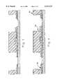
- FIG. 7is a cross sectional view of the device of the present invention after backside wafer processing has been completed.
- FIG. 8is a cross sectional view of the structure of FIG. 7 flip-chip mounted on a substrate.
- a coating processis comprised of applying a sufficient coating of a low dielectric polymer, preferably benzocylclobutane, 10 upon a processed wafer 1 which is a preferably gallium arsenide or another suitable semi-insulating or insulating substrate.
- the region 2distinguishes the region of the wafer 1 which has been implanted with a suitable implant ion such as boron to effect required isolation between active devices (such as the MESFET 7) as is well known to one of ordinary skill in the art.
- the MMIC processalso has other various components, well known in the art, such as airbridges 3, capacitors 4, streets 5, bond pads 6, and field effect transistors 7 (FET) overlying and attached to the gallium arsenide wafer 1.
- the low dielectric polymer 10is removed from all bond pads 6 and streets 5 of the MMIC wafer 1, as illustrated in FIG. 3, by first photoexposing the polymer through a negative mask (not shown), and then rinsing the polymer with a conventional polymeric solvent, such as Stoddard solvent or other suitable developers (not shown). The low dielectric polymer is then cured at a low temperature upon the processed MMIC wafer.
- a ceramic coating 401is deposited over the low dielectric polymer coated MMIC wafer.
- the ceramicpreferably silicon carbide or silicon nitride is deposited in a thickness on the order of 0.5 microns.
- the ceramic coatingis removed from all bond pads 6 and streets 5 of the MMIC wafer 1, as illustrated in FIG.
- FIG. 5by first coating the ceramic with a positive photoresist material, like AZ5200 (not shown), photoexposing the resist through a positive mask (not shown), and then rinsing the resist with a conventional resist developer. The exposed areas of the ceramic coating are then etched using conventional RIE (reactive ion etching) techniques, as illustrated in FIG. 5.
- the solder bumps 601are disposed on the front side surface of the MMIC as shown.
- the bumpshard bumps or solder bumps
- FIG. 7illustrates, the polymeric and ceramic coated processed MMIC is finished by backside processing to effect the desired product, by steps well known to the artisan of ordinary skill.
- FIG. 8is a view of the finished MMIC wafer having polymeric coating overlaid by a ceramic coating flip chip mounted to a suitable carrier 802 utilizing underfill material 803.
- the low dielectric polymerpossesses mechanical, electrical and chemical properties that make it compatible with MMIC fabrication processes and capable of use in high-speed MMIC's without the ill effects of capacitance related losses.
- the low dielectric polymeris preferably spin-coatable and photo-imageable so that the polymer can be patterned using simple photolithography techniques.
- the polymerwould preferably have a low loss tangent, like 0.002 at 10 Ghz, which allows for minimum perturbation in the microwave performance of the MMIC device.
- Such low dielectric polymerssuch as an arylcyclobutene like benzocyclobutene (BCB) as disclosed in U.S. Pat. No.
- the polymerIn addition to its favorable low dielectric constant the polymer also provides sufficient resistance to moisture. This sufficient resistance to moisture is increased by overlaying a ceramic layer, like SiC, upon the low dielectric polymer and other pre-determined areas.
- the polymerprovides excellent resistance to mechanical damage during subsequent processing and in particular during final assemble.
- the process of encapsulating the MMICentails spinning upon the MMIC a uniform coat (known as spin-coating) of the photosensitive, low dielectric polymer and then patterning the polymer using standard photolithography techniques, so that predetermined areas are coated with the BCB, and other areas like bond pads and wafer streets upon the MMIC are exposed.
- the uniform coatingis sufficiently thick to cover the tallest structure on the MMIC, such as air bridges, which usually require about 8 to 10 microns of the polymer.
- the preferred thickness for capacitive decouplingis as little as 7-8 microns.
- the polymeris then cured at 250C in a vacuum oven under a nitrogen atmosphere for about an hour.
- the ceramic layerpreferably SiC is deposited upon the polymer and the remaining portions of the MMIC by Plasma Enhanced Chemical Vapor Deposition (PECVD) at 250C as referenced in M. Loboda, "Low Temperature PECVD Growth and Characterization of SiC:H. Films Deposited from Silacyclobutane and Silanel Methane Precursor Gases" in Amorphous and Crystalline Silicon Carbide IV, C4 Yang, M. M. Rahman and G. L. Harris, eds; Springer Proc. In Physics (Springer Verlag, Berlin Heidelberg), 71, p. 271-280, 1992, the disclosure of which is specifically incorporated herein by reference.
- the ceramic layeris then patterned using a standard photoresist layer as the etch mask and etched using Reactive Ion Etching Techniques. Again, the ceramic layer like the polymer leaves portions of the MMIC like bond pads and wafer streets open.
- solder bumps 601are disposed on the front side surface of the MMIC as shown.
- the bumps(hard bumps or solder bumps) are formed on the bonding pads using electroplating.
- the wafer backside processingis carried out (if needed), which is generally a standard wafer thinning and metallization to provide a ground plane for the integrated circuit.
- the MMICis shown at 801 with the bumps 601 clearly shown.
- the carrier substrateis shown at 802 with the filler material shown at 803.
- the carrier substratecan be for example electronics grade glass or other material well known to one of ordinary skill in the art.
- the final versionhas the attendant advantages as described above in that flip-chip mounting is enabled by the version of the present disclosure by virtue of the encapsulating material BCB and the ceramic layer silicon carbide having virtually no deleterious effects on the performance of the device.
- the filler material which is used to reduce the stress between the solder bumps 601 and the carrier substrate 802has no adverse effect on the performance of the integrated circuit because the thickness of the layer of BCB enables the MMIC to be capacitively decoupled from the package.
- the solder bumps 601 of the present disclosurehaving thickness on the order of 3 to 4 mils. These are formed generally by standard metal electroplating or evaporation well known to one of ordinary skill in the art.
- the filler materialis conventional polymer well known to one of ordinary skill in the art to include such as Dexter Hysol 4526.
Landscapes
- Engineering & Computer Science (AREA)
- Computer Hardware Design (AREA)
- Microelectronics & Electronic Packaging (AREA)
- Power Engineering (AREA)
- Physics & Mathematics (AREA)
- Condensed Matter Physics & Semiconductors (AREA)
- General Physics & Mathematics (AREA)
- Structures Or Materials For Encapsulating Or Coating Semiconductor Devices Or Solid State Devices (AREA)
Abstract
Description
Claims (24)
Priority Applications (1)
| Application Number | Priority Date | Filing Date | Title |
|---|---|---|---|
| US09/019,627US6137125A (en) | 1995-12-21 | 1998-02-06 | Two layer hermetic-like coating for on-wafer encapsulatuon of GaAs MMIC's having flip-chip bonding capabilities |
Applications Claiming Priority (3)
| Application Number | Priority Date | Filing Date | Title |
|---|---|---|---|
| US57652495A | 1995-12-21 | 1995-12-21 | |
| US08/863,759US5914508A (en) | 1995-12-21 | 1997-05-27 | Two layer hermetic-like coating process for on-wafer encapsulation of GaAs MMIC's |
| US09/019,627US6137125A (en) | 1995-12-21 | 1998-02-06 | Two layer hermetic-like coating for on-wafer encapsulatuon of GaAs MMIC's having flip-chip bonding capabilities |
Related Parent Applications (1)
| Application Number | Title | Priority Date | Filing Date |
|---|---|---|---|
| US08/863,759Continuation-In-PartUS5914508A (en) | 1995-12-21 | 1997-05-27 | Two layer hermetic-like coating process for on-wafer encapsulation of GaAs MMIC's |
Publications (1)
| Publication Number | Publication Date |
|---|---|
| US6137125Atrue US6137125A (en) | 2000-10-24 |
Family
ID=27076969
Family Applications (1)
| Application Number | Title | Priority Date | Filing Date |
|---|---|---|---|
| US09/019,627Expired - LifetimeUS6137125A (en) | 1995-12-21 | 1998-02-06 | Two layer hermetic-like coating for on-wafer encapsulatuon of GaAs MMIC's having flip-chip bonding capabilities |
Country Status (1)
| Country | Link |
|---|---|
| US (1) | US6137125A (en) |
Cited By (24)
| Publication number | Priority date | Publication date | Assignee | Title |
|---|---|---|---|---|
| US20030134233A1 (en)* | 2002-01-16 | 2003-07-17 | Taiwan Semiconductor Manufacturing Co., Ltd. | Method of forming a solder ball using a thermally stable resinous protective layer |
| US6597066B1 (en)* | 1996-03-12 | 2003-07-22 | Micron Technology, Inc. | Hermetic chip and method of manufacture |
| DE10300958A1 (en)* | 2003-01-13 | 2004-07-22 | Epcos Ag | Encapsulated module |
| US6855613B1 (en)* | 1999-11-04 | 2005-02-15 | Lucent Technologies Inc. | Method of fabricating a heterojunction bipolar transistor |
| US7094618B2 (en) | 2000-08-25 | 2006-08-22 | Micron Technology, Inc. | Methods for marking a packaged semiconductor die including applying tape and subsequently marking the tape |
| US20070001314A1 (en)* | 2005-01-07 | 2007-01-04 | Seoul National University Industry Foundation | Flip-chip bonding structure using multi chip module-deposited substrate |
| US7169685B2 (en) | 2002-02-25 | 2007-01-30 | Micron Technology, Inc. | Wafer back side coating to balance stress from passivation layer on front of wafer and be used as die attach adhesive |
| US20080227302A1 (en)* | 2007-03-12 | 2008-09-18 | Honeywell International Inc. | Fibrous laminate interface for security coatings |
| WO2012033641A1 (en)* | 2010-09-10 | 2012-03-15 | Raytheon Company | Monolithic microwave integrated circuit |
| US8143654B1 (en)* | 2008-01-16 | 2012-03-27 | Triquint Semiconductor, Inc. | Monolithic microwave integrated circuit with diamond layer |
| US20200235054A1 (en) | 2019-01-23 | 2020-07-23 | Qorvo Us, Inc. | Rf devices with enhanced performance and methods of forming the same |
| US20210134699A1 (en)* | 2019-11-01 | 2021-05-06 | Qorvo Us, Inc. | Rf devices with nanotube particles for enhanced performance and methods of forming the same |
| US20210296199A1 (en) | 2018-11-29 | 2021-09-23 | Qorvo Us, Inc. | Thermally enhanced semiconductor package with at least one heat extractor and process for making the same |
| US20220108938A1 (en) | 2019-01-23 | 2022-04-07 | Qorvo Us, Inc. | Rf devices with enhanced performance and methods of forming the same |
| US20220139862A1 (en) | 2019-01-23 | 2022-05-05 | Qorvo Us, Inc. | Rf devices with enhanced performance and methods of forming the same |
| US11646289B2 (en) | 2019-12-02 | 2023-05-09 | Qorvo Us, Inc. | RF devices with enhanced performance and methods of forming the same |
| US11923238B2 (en) | 2019-12-12 | 2024-03-05 | Qorvo Us, Inc. | Method of forming RF devices with enhanced performance including attaching a wafer to a support carrier by a bonding technique without any polymer adhesive |
| US12046505B2 (en) | 2018-04-20 | 2024-07-23 | Qorvo Us, Inc. | RF devices with enhanced performance and methods of forming the same utilizing localized SOI formation |
| US12046483B2 (en) | 2019-01-23 | 2024-07-23 | Qorvo Us, Inc. | RF devices with enhanced performance and methods of forming the same |
| US12046535B2 (en) | 2018-07-02 | 2024-07-23 | Qorvo Us, Inc. | RF devices with enhanced performance and methods of forming the same |
| US12062700B2 (en) | 2018-04-04 | 2024-08-13 | Qorvo Us, Inc. | Gallium-nitride-based module with enhanced electrical performance and process for making the same |
| US12062571B2 (en) | 2021-03-05 | 2024-08-13 | Qorvo Us, Inc. | Selective etching process for SiGe and doped epitaxial silicon |
| US12125825B2 (en) | 2019-01-23 | 2024-10-22 | Qorvo Us, Inc. | RF devices with enhanced performance and methods of forming the same |
| US12129168B2 (en) | 2019-12-23 | 2024-10-29 | Qorvo Us, Inc. | Microelectronics package with vertically stacked MEMS device and controller device |
Citations (16)
| Publication number | Priority date | Publication date | Assignee | Title |
|---|---|---|---|---|
| US3811183A (en)* | 1971-02-05 | 1974-05-21 | Philips Corp | Method of manufacturing a semiconductor device and semiconductor device manufactured by the method |
| US4714516A (en)* | 1986-09-26 | 1987-12-22 | General Electric Company | Method to produce via holes in polymer dielectrics for multiple electronic circuit chip packaging |
| US4737236A (en)* | 1986-09-08 | 1988-04-12 | M/A-Com, Inc. | Method of making microwave integrated circuits |
| US4780177A (en)* | 1988-02-05 | 1988-10-25 | General Electric Company | Excimer laser patterning of a novel resist |
| US4783695A (en)* | 1986-09-26 | 1988-11-08 | General Electric Company | Multichip integrated circuit packaging configuration and method |
| US4835704A (en)* | 1986-12-29 | 1989-05-30 | General Electric Company | Adaptive lithography system to provide high density interconnect |
| US4894115A (en)* | 1989-02-14 | 1990-01-16 | General Electric Company | Laser beam scanning method for forming via holes in polymer materials |
| US5073814A (en)* | 1990-07-02 | 1991-12-17 | General Electric Company | Multi-sublayer dielectric layers |
| US5154793A (en)* | 1988-09-27 | 1992-10-13 | General Electric Company | Method and apparatus for removing components bonded to a substrate |
| US5171824A (en)* | 1990-12-24 | 1992-12-15 | The Dow Chemical Company | Process for the preparation of arylcyclobutene terminated condensation polymers |
| US5198527A (en)* | 1990-12-24 | 1993-03-30 | The Dow Chemical Company | Arylcyclobutene terminated carbonate polymer |
| US5246782A (en)* | 1990-12-10 | 1993-09-21 | The Dow Chemical Company | Laminates of polymers having perfluorocyclobutane rings and polymers containing perfluorocyclobutane rings |
| US5311153A (en)* | 1992-07-17 | 1994-05-10 | Trw Inc. | Integrated waveguide/stripline transition |
| US5461545A (en)* | 1990-08-24 | 1995-10-24 | Thomson-Csf | Process and device for hermetic encapsulation of electronic components |
| US5497033A (en)* | 1993-02-08 | 1996-03-05 | Martin Marietta Corporation | Embedded substrate for integrated circuit modules |
| US5914508A (en)* | 1995-12-21 | 1999-06-22 | The Whitaker Corporation | Two layer hermetic-like coating process for on-wafer encapsulation of GaAs MMIC's |
- 1998
- 1998-02-06USUS09/019,627patent/US6137125A/ennot_activeExpired - Lifetime
Patent Citations (17)
| Publication number | Priority date | Publication date | Assignee | Title |
|---|---|---|---|---|
| US3811183A (en)* | 1971-02-05 | 1974-05-21 | Philips Corp | Method of manufacturing a semiconductor device and semiconductor device manufactured by the method |
| US4737236A (en)* | 1986-09-08 | 1988-04-12 | M/A-Com, Inc. | Method of making microwave integrated circuits |
| US4714516A (en)* | 1986-09-26 | 1987-12-22 | General Electric Company | Method to produce via holes in polymer dielectrics for multiple electronic circuit chip packaging |
| US4783695A (en)* | 1986-09-26 | 1988-11-08 | General Electric Company | Multichip integrated circuit packaging configuration and method |
| US4835704A (en)* | 1986-12-29 | 1989-05-30 | General Electric Company | Adaptive lithography system to provide high density interconnect |
| US4780177A (en)* | 1988-02-05 | 1988-10-25 | General Electric Company | Excimer laser patterning of a novel resist |
| US5154793A (en)* | 1988-09-27 | 1992-10-13 | General Electric Company | Method and apparatus for removing components bonded to a substrate |
| US4894115A (en)* | 1989-02-14 | 1990-01-16 | General Electric Company | Laser beam scanning method for forming via holes in polymer materials |
| US5073814A (en)* | 1990-07-02 | 1991-12-17 | General Electric Company | Multi-sublayer dielectric layers |
| US5461545A (en)* | 1990-08-24 | 1995-10-24 | Thomson-Csf | Process and device for hermetic encapsulation of electronic components |
| US5246782A (en)* | 1990-12-10 | 1993-09-21 | The Dow Chemical Company | Laminates of polymers having perfluorocyclobutane rings and polymers containing perfluorocyclobutane rings |
| US5409777A (en)* | 1990-12-10 | 1995-04-25 | The Dow Chemical Company | Laminates of polymer shaving perfluorocyclobutane rings |
| US5171824A (en)* | 1990-12-24 | 1992-12-15 | The Dow Chemical Company | Process for the preparation of arylcyclobutene terminated condensation polymers |
| US5198527A (en)* | 1990-12-24 | 1993-03-30 | The Dow Chemical Company | Arylcyclobutene terminated carbonate polymer |
| US5311153A (en)* | 1992-07-17 | 1994-05-10 | Trw Inc. | Integrated waveguide/stripline transition |
| US5497033A (en)* | 1993-02-08 | 1996-03-05 | Martin Marietta Corporation | Embedded substrate for integrated circuit modules |
| US5914508A (en)* | 1995-12-21 | 1999-06-22 | The Whitaker Corporation | Two layer hermetic-like coating process for on-wafer encapsulation of GaAs MMIC's |
Non-Patent Citations (14)
| Title |
|---|
| A. Phostosensitive BCB on Laminate Technology (MCM LD) ; IEEE Jan. 5, 1994 pp. 374 386.* |
| A. Phostosensitive--BCB on Laminate Technology (MCM-LD) ; IEEE Jan. 5, 1994 pp. 374-386. |
| Abstract: 1995 IEEE; High Performance Microwave elements for SiGe MMICs, Michael Case, perry MacDonald, Mehran Matloubian, Mary Chen, Larry Larson and David Rensch, pp. 85 95.* |
| Abstract: 1995 IEEE; High Performance Microwave elements for SiGe MMICs, Michael Case, perry MacDonald, Mehran Matloubian, Mary Chen, Larry Larson and David Rensch, pp. 85-95. |
| Abstract: ISHM 94 Proceedings M 4 CMx (Thin Film Multi MMIC Multi IC Modules) for Microwave Applications. Ernst Feurer, Martin Oppermann and Bruno Hall.* |
| Abstract: ISHM '94 Proceedings M4 CMx (Thin Film Multi-MMIC Multi--IC Modules) for Microwave Applications. Ernst Feurer, Martin Oppermann and Bruno Hall. |
| Abstract: Processing and Electrical Charzcterization of Multilayer Metallization For Microwave Applications, Percy B. Chinoy, M/A Com, Inc Apr. 1995.* |
| Abstract: Processing and Electrical Charzcterization of Multilayer Metallization For Microwave Applications, Percy B. Chinoy, M/A-Com, Inc Apr. 1995. |
| Amorphous and Crystalline Silicon Carbide IV; Proceedings of the 4 th INternational conference, Santa Clara, CA, Oct. 9 11, 1991, Springer Verlag, C.Y. yang, M.M. Rahman, G.L. harris (Eds.) pp. 271 280.* |
| Amorphous and Crystalline Silicon Carbide IV; Proceedings of the 4th INternational conference, Santa Clara, CA, Oct. 9-11, 1991, Springer-Verlag, C.Y. yang, M.M. Rahman, G.L. harris (Eds.) pp. 271-280. |
| Concise Chemical and Technical Dictionary; Edited by H. Bennett, F.A.I.C., Director, B.R. Laboratories, Miami Beach, FL Chemical Publishing Co., Inc.pp. 573 and279.* |
| IEEE Transactions on components, Hybrids, and Manufacturing Technology, vol. 16, NO. 7, Nov. 1993. Processing and Microwave Characterizaton of Multilevel Interconects Using Benzocyclobutene Dielectric, Percy B. Chinoy, and James Tajadod.* |
| Inside Engineering . . . Balun Transformers For RF Chip Sets, Mixers and Broadband Impedance Matching, Feb. 1995, M/A Com Loud & Clear /3., by Simon Gay.* |
| Inside Engineering . . . Balun Transformers For RF Chip Sets, Mixers and Broadband Impedance Matching, Feb. 1995, M/A-Com Loud & Clear /3., by Simon Gay. |
Cited By (50)
| Publication number | Priority date | Publication date | Assignee | Title |
|---|---|---|---|---|
| US20060022337A1 (en)* | 1996-03-12 | 2006-02-02 | Farnworth Warren M | Hermetic chip in wafer form |
| US6597066B1 (en)* | 1996-03-12 | 2003-07-22 | Micron Technology, Inc. | Hermetic chip and method of manufacture |
| US20040051184A1 (en)* | 1996-03-12 | 2004-03-18 | Farnworth Warren M. | Hermetic chip and method of manufacture |
| US6815314B2 (en) | 1996-03-12 | 2004-11-09 | Micron Technology, Inc. | Hermetic chip and method of manufacture |
| US6953995B2 (en) | 1996-03-12 | 2005-10-11 | Micron Technology, Inc. | Hermetic chip in wafer form |
| US6855613B1 (en)* | 1999-11-04 | 2005-02-15 | Lucent Technologies Inc. | Method of fabricating a heterojunction bipolar transistor |
| US7238543B2 (en) | 2000-08-25 | 2007-07-03 | Micron Technology, Inc. | Methods for marking a bare semiconductor die including applying a tape having energy-markable properties |
| US7094618B2 (en) | 2000-08-25 | 2006-08-22 | Micron Technology, Inc. | Methods for marking a packaged semiconductor die including applying tape and subsequently marking the tape |
| US6974659B2 (en)* | 2002-01-16 | 2005-12-13 | Taiwan Semiconductor Manufacturing Co., Ltd. | Method of forming a solder ball using a thermally stable resinous protective layer |
| US20030134233A1 (en)* | 2002-01-16 | 2003-07-17 | Taiwan Semiconductor Manufacturing Co., Ltd. | Method of forming a solder ball using a thermally stable resinous protective layer |
| US7727785B2 (en) | 2002-02-25 | 2010-06-01 | Micron Technology, Inc. | Wafer back side coating to balance stress from passivation layer on front of wafer and be used as die attach adhesive |
| US7169685B2 (en) | 2002-02-25 | 2007-01-30 | Micron Technology, Inc. | Wafer back side coating to balance stress from passivation layer on front of wafer and be used as die attach adhesive |
| US20060103003A1 (en)* | 2003-01-13 | 2006-05-18 | Patric Heide | Modular construction component with encapsulation |
| WO2004064152A3 (en)* | 2003-01-13 | 2005-09-09 | Epcos Ag | Modular construction component with encapsulation |
| DE10300958A1 (en)* | 2003-01-13 | 2004-07-22 | Epcos Ag | Encapsulated module |
| US20070001314A1 (en)* | 2005-01-07 | 2007-01-04 | Seoul National University Industry Foundation | Flip-chip bonding structure using multi chip module-deposited substrate |
| US7375428B2 (en) | 2005-01-07 | 2008-05-20 | Seoul National University Industry Foundation | Flip-chip bonding structure using multi chip module-deposited substrate |
| US20080227302A1 (en)* | 2007-03-12 | 2008-09-18 | Honeywell International Inc. | Fibrous laminate interface for security coatings |
| US8710618B2 (en) | 2007-03-12 | 2014-04-29 | Honeywell International Inc. | Fibrous laminate interface for security coatings |
| US8921971B2 (en) | 2007-03-12 | 2014-12-30 | Honeywell International Inc. | Fibrous laminate interface for security coatings |
| US8143654B1 (en)* | 2008-01-16 | 2012-03-27 | Triquint Semiconductor, Inc. | Monolithic microwave integrated circuit with diamond layer |
| WO2012033641A1 (en)* | 2010-09-10 | 2012-03-15 | Raytheon Company | Monolithic microwave integrated circuit |
| US8339790B2 (en)* | 2010-09-10 | 2012-12-25 | Raytheon Company | Monolithic microwave integrated circuit |
| US12062701B2 (en) | 2018-04-04 | 2024-08-13 | Qorvo Us, Inc. | Gallium-nitride-based module with enhanced electrical performance and process for making the same |
| US12062700B2 (en) | 2018-04-04 | 2024-08-13 | Qorvo Us, Inc. | Gallium-nitride-based module with enhanced electrical performance and process for making the same |
| US12125739B2 (en) | 2018-04-20 | 2024-10-22 | Qorvo Us, Inc. | RF devices with enhanced performance and methods of forming the same utilizing localized SOI formation |
| US12046505B2 (en) | 2018-04-20 | 2024-07-23 | Qorvo Us, Inc. | RF devices with enhanced performance and methods of forming the same utilizing localized SOI formation |
| US12165951B2 (en) | 2018-07-02 | 2024-12-10 | Qorvo Us, Inc. | RF devices with enhanced performance and methods of forming the same |
| US12046535B2 (en) | 2018-07-02 | 2024-07-23 | Qorvo Us, Inc. | RF devices with enhanced performance and methods of forming the same |
| US20210296199A1 (en) | 2018-11-29 | 2021-09-23 | Qorvo Us, Inc. | Thermally enhanced semiconductor package with at least one heat extractor and process for making the same |
| US11942389B2 (en) | 2018-11-29 | 2024-03-26 | Qorvo Us, Inc. | Thermally enhanced semiconductor package with at least one heat extractor and process for making the same |
| US11646242B2 (en) | 2018-11-29 | 2023-05-09 | Qorvo Us, Inc. | Thermally enhanced semiconductor package with at least one heat extractor and process for making the same |
| US20200235054A1 (en) | 2019-01-23 | 2020-07-23 | Qorvo Us, Inc. | Rf devices with enhanced performance and methods of forming the same |
| US20220139862A1 (en) | 2019-01-23 | 2022-05-05 | Qorvo Us, Inc. | Rf devices with enhanced performance and methods of forming the same |
| US11923313B2 (en) | 2019-01-23 | 2024-03-05 | Qorvo Us, Inc. | RF device without silicon handle substrate for enhanced thermal and electrical performance and methods of forming the same |
| US12046483B2 (en) | 2019-01-23 | 2024-07-23 | Qorvo Us, Inc. | RF devices with enhanced performance and methods of forming the same |
| US12046570B2 (en) | 2019-01-23 | 2024-07-23 | Qorvo Us, Inc. | RF devices with enhanced performance and methods of forming the same |
| US11961813B2 (en) | 2019-01-23 | 2024-04-16 | Qorvo Us, Inc. | RF devices with enhanced performance and methods of forming the same |
| US12057374B2 (en) | 2019-01-23 | 2024-08-06 | Qorvo Us, Inc. | RF devices with enhanced performance and methods of forming the same |
| US12125825B2 (en) | 2019-01-23 | 2024-10-22 | Qorvo Us, Inc. | RF devices with enhanced performance and methods of forming the same |
| US12062623B2 (en) | 2019-01-23 | 2024-08-13 | Qorvo Us, Inc. | RF device without silicon handle substrate for enhanced thermal and electrical performance and methods of forming the same |
| US12368056B2 (en) | 2019-01-23 | 2025-07-22 | Qorvo Us, Inc. | RF devices with enhanced performance and methods of forming the same |
| US20220108938A1 (en) | 2019-01-23 | 2022-04-07 | Qorvo Us, Inc. | Rf devices with enhanced performance and methods of forming the same |
| US12112999B2 (en) | 2019-01-23 | 2024-10-08 | Qorvo Us, Inc. | RF devices with enhanced performance and methods of forming the same |
| US12074086B2 (en)* | 2019-11-01 | 2024-08-27 | Qorvo Us, Inc. | RF devices with nanotube particles for enhanced performance and methods of forming the same |
| US20210134699A1 (en)* | 2019-11-01 | 2021-05-06 | Qorvo Us, Inc. | Rf devices with nanotube particles for enhanced performance and methods of forming the same |
| US11646289B2 (en) | 2019-12-02 | 2023-05-09 | Qorvo Us, Inc. | RF devices with enhanced performance and methods of forming the same |
| US11923238B2 (en) | 2019-12-12 | 2024-03-05 | Qorvo Us, Inc. | Method of forming RF devices with enhanced performance including attaching a wafer to a support carrier by a bonding technique without any polymer adhesive |
| US12129168B2 (en) | 2019-12-23 | 2024-10-29 | Qorvo Us, Inc. | Microelectronics package with vertically stacked MEMS device and controller device |
| US12062571B2 (en) | 2021-03-05 | 2024-08-13 | Qorvo Us, Inc. | Selective etching process for SiGe and doped epitaxial silicon |
Similar Documents
| Publication | Publication Date | Title |
|---|---|---|
| US6137125A (en) | Two layer hermetic-like coating for on-wafer encapsulatuon of GaAs MMIC's having flip-chip bonding capabilities | |
| US6322903B1 (en) | Package of integrated circuits and vertical integration | |
| US7629201B2 (en) | Method for fabricating a wafer level package with device wafer and passive component integration | |
| CN102099282B (en) | Method for packaging semiconductors at wafer level | |
| US12148717B2 (en) | Through wafer trench isolation between transistors in an integrated circuit | |
| US7709954B2 (en) | Redistribution layer for wafer-level chip scale package and method therefor | |
| US11158520B2 (en) | Method to protect die during metal-embedded chip assembly (MECA) process | |
| US6001673A (en) | Methods for packaging integrated circuit devices including cavities adjacent active regions | |
| US7935607B2 (en) | Integrated passive device with a high resistivity substrate and method for forming the same | |
| US5914508A (en) | Two layer hermetic-like coating process for on-wafer encapsulation of GaAs MMIC's | |
| KR20100044165A (en) | Method for packaging semiconductors at a wafer level | |
| US20210210538A1 (en) | Chip package and method for forming the same | |
| US8653673B2 (en) | Method for packaging semiconductors at a wafer level | |
| US8102044B2 (en) | Bonded wafer structure and method of fabrication | |
| Kaleta et al. | A two layer hermetic-like coating process for on-wafer encapsulation of GaAs MMICs | |
| US9093394B1 (en) | Method and structure for encapsulation and interconnection of transistors | |
| US12424567B2 (en) | Chip package and manufacturing method thereof | |
| US20250157988A1 (en) | 3d-ic for rf applications | |
| Yoshida et al. | A new millimeter-wave IC on Si substrate using MBB technology | |
| JP2024527523A (en) | Improved Q factor of passive components with resistively elevated regions of substrate - Patents.com | |
| KR19980015648A (en) | Manufacturing method of porous silicon layer with selective oxide film and multichip packaging application | |
| GB2268327A (en) | Passivated gallium arsenide device | |
| JPH11297926A (en) | Semiconductor device |
Legal Events
| Date | Code | Title | Description |
|---|---|---|---|
| AS | Assignment | Owner name:UNITED STATES AIR FORCE, VIRGINIA Free format text:CONFIRMATORY LICENSE;ASSIGNOR:M/A-COM, A DIVISION OF AMP INCORPORATED;REEL/FRAME:009606/0363 Effective date:19980923 | |
| STCF | Information on status: patent grant | Free format text:PATENTED CASE | |
| FPAY | Fee payment | Year of fee payment:4 | |
| FPAY | Fee payment | Year of fee payment:8 | |
| REMI | Maintenance fee reminder mailed | ||
| AS | Assignment | Owner name:COBHAM DEFENSE ELECTRONIC SYSTEMS CORPORATION, MAS Free format text:ASSIGNMENT OF ASSIGNORS INTEREST;ASSIGNORS:M/A COM, INC.;RAYCHEM INTERNATIONAL;TYCO ELECTRONICS CORPORATION;AND OTHERS;REEL/FRAME:022266/0400;SIGNING DATES FROM 20080108 TO 20090113 Owner name:COBHAM DEFENSE ELECTRONIC SYSTEMS CORPORATION,MASS Free format text:ASSIGNMENT OF ASSIGNORS INTEREST;ASSIGNORS:M/A COM, INC.;RAYCHEM INTERNATIONAL;TYCO ELECTRONICS CORPORATION;AND OTHERS;SIGNING DATES FROM 20080108 TO 20090113;REEL/FRAME:022266/0400 Owner name:COBHAM DEFENSE ELECTRONIC SYSTEMS CORPORATION, MAS Free format text:ASSIGNMENT OF ASSIGNORS INTEREST;ASSIGNORS:M/A COM, INC.;RAYCHEM INTERNATIONAL;TYCO ELECTRONICS CORPORATION;AND OTHERS;SIGNING DATES FROM 20080108 TO 20090113;REEL/FRAME:022266/0400 | |
| AS | Assignment | Owner name:COBHAM DEFENSE ELECTRONIC SYSTEMS CORPORATION, MAS Free format text:SECURITY AGREEMENT;ASSIGNOR:KIWI STONE ACQUISITION CORP.;REEL/FRAME:022482/0016 Effective date:20090330 Owner name:COBHAM DEFENSE ELECTRONIC SYSTEMS CORPORATION,MASS Free format text:SECURITY AGREEMENT;ASSIGNOR:KIWI STONE ACQUISITION CORP.;REEL/FRAME:022482/0016 Effective date:20090330 | |
| AS | Assignment | Owner name:KIWI STONE ACQUISITION CORPORATION, CALIFORNIA Free format text:ASSIGNMENT OF ASSIGNORS INTEREST;ASSIGNOR:COBHAM DEFENSE ELECTRONIC SYSTEMS CORPORATION;REEL/FRAME:022714/0890 Effective date:20090521 Owner name:KIWI STONE ACQUISITION CORPORATION,CALIFORNIA Free format text:ASSIGNMENT OF ASSIGNORS INTEREST;ASSIGNOR:COBHAM DEFENSE ELECTRONIC SYSTEMS CORPORATION;REEL/FRAME:022714/0890 Effective date:20090521 | |
| AS | Assignment | Owner name:M/A-COM TECHNOLOGY SOLUTIONS HOLDINGS, INC., MASSA Free format text:CHANGE OF NAME;ASSIGNOR:KIWI STONE ACQUISITION CORP.;REEL/FRAME:023476/0069 Effective date:20090526 Owner name:M/A-COM TECHNOLOGY SOLUTIONS HOLDINGS, INC.,MASSAC Free format text:CHANGE OF NAME;ASSIGNOR:KIWI STONE ACQUISITION CORP.;REEL/FRAME:023476/0069 Effective date:20090526 | |
| AS | Assignment | Owner name:RBS BUSINESS CAPITAL, A DIVISION OF RBS ASSET FINA Free format text:SECURITY AGREEMENT;ASSIGNORS:MIMIX BROADBAND, INC.;M/A-COM TECHNOLOGY SOLUTIONS HOLDINGS, INC.;REEL/FRAME:025444/0920 Effective date:20101203 | |
| AS | Assignment | Owner name:JPMORGAN CHASE BANK, N.A., AS ADMINISTRATIVE AGENT Free format text:SECURITY AGREEMENT;ASSIGNOR:M/A-COM TECHNOLOGY SOLUTIONS HOLDINGS, INC.;REEL/FRAME:027015/0444 Effective date:20110930 | |
| AS | Assignment | Owner name:MIMIX BROADBAND, INC., MASSACHUSETTS Free format text:RELEASE OF SECURITY INTEREST RECORDED AT REEL/FRAME 25444/920;ASSIGNOR:RBS BUSINESS CAPITAL, A DIVISION OF RBS ASSET FINANCE, INC., AS ADMINISTRATIVE AGENT;REEL/FRAME:027028/0021 Effective date:20110930 Owner name:M/A-COM TECHNOLOGY SOLUTIONS HOLDINGS, INC., MASSA Free format text:RELEASE OF SECURITY INTEREST RECORDED AT REEL/FRAME 25444/920;ASSIGNOR:RBS BUSINESS CAPITAL, A DIVISION OF RBS ASSET FINANCE, INC., AS ADMINISTRATIVE AGENT;REEL/FRAME:027028/0021 Effective date:20110930 | |
| FPAY | Fee payment | Year of fee payment:12 | |
| AS | Assignment | Owner name:JPMORGAN CHASE BANK, N.A., AS ADMINISTRATIVE AGENT Free format text:SECURITY AGREEMENT;ASSIGNOR:M/A-COM TECHNOLOGY SOLUTIONS HOLDINGS, INC.;REEL/FRAME:031314/0183 Effective date:20130926 | |
| AS | Assignment | Owner name:M/A-COM TECHNOLOGY SOLUTIONS HOLDINGS, INC., MASSA Free format text:RELEASE BY SECURED PARTY;ASSIGNOR:JPMORGAN CHASE BANK, N.A.;REEL/FRAME:032857/0032 Effective date:20140508 | |
| AS | Assignment | Owner name:GOLDMAN SACHS BANK USA, NEW YORK Free format text:SECURITY INTEREST;ASSIGNORS:M/A-COM TECHNOLOGY SOLUTIONS HOLDINGS, INC.;MINDSPEED TECHNOLOGIES, INC.;BROOKTREE CORPORATION;REEL/FRAME:032859/0374 Effective date:20140508 |