US6136689A - Method of forming a micro solder ball for use in C4 bonding process - Google Patents
Method of forming a micro solder ball for use in C4 bonding processDownload PDFInfo
- Publication number
- US6136689A US6136689AUS09/134,363US13436398AUS6136689AUS 6136689 AUS6136689 AUS 6136689AUS 13436398 AUS13436398 AUS 13436398AUS 6136689 AUS6136689 AUS 6136689A
- Authority
- US
- United States
- Prior art keywords
- solder
- layer
- photoresist
- contacts
- tape
- Prior art date
- Legal status (The legal status is an assumption and is not a legal conclusion. Google has not performed a legal analysis and makes no representation as to the accuracy of the status listed.)
- Expired - Lifetime
Links
- 229910000679solderInorganic materials0.000titleclaimsabstractdescription136
- 238000000034methodMethods0.000titleclaimsabstractdescription123
- 230000008569processEffects0.000titleclaimsabstractdescription81
- 229920002120photoresistant polymerPolymers0.000claimsabstractdescription78
- 238000000151depositionMethods0.000claimsabstractdescription13
- 239000002184metalSubstances0.000claimsdescription61
- 229910052751metalInorganic materials0.000claimsdescription61
- 239000000758substrateSubstances0.000claimsdescription35
- VYPSYNLAJGMNEJ-UHFFFAOYSA-NSilicium dioxideChemical groupO=[Si]=OVYPSYNLAJGMNEJ-UHFFFAOYSA-N0.000claimsdescription14
- PXHVJJICTQNCMI-UHFFFAOYSA-NNickelChemical compound[Ni]PXHVJJICTQNCMI-UHFFFAOYSA-N0.000claimsdescription9
- 239000004642PolyimideSubstances0.000claimsdescription7
- 239000010931goldSubstances0.000claimsdescription7
- 229920001721polyimidePolymers0.000claimsdescription7
- 239000000377silicon dioxideSubstances0.000claimsdescription7
- 239000002390adhesive tapeSubstances0.000claimsdescription6
- 239000010949copperSubstances0.000claimsdescription6
- 235000012239silicon dioxideNutrition0.000claimsdescription6
- 229910052581Si3N4Inorganic materials0.000claimsdescription5
- 229910052737goldInorganic materials0.000claimsdescription5
- HQVNEWCFYHHQES-UHFFFAOYSA-Nsilicon nitrideChemical compoundN12[Si]34N5[Si]62N3[Si]51N64HQVNEWCFYHHQES-UHFFFAOYSA-N0.000claimsdescription5
- 241000206607Porphyra umbilicalisSpecies0.000claimsdescription4
- 229910052802copperInorganic materials0.000claimsdescription4
- PCHJSUWPFVWCPO-UHFFFAOYSA-NgoldChemical compound[Au]PCHJSUWPFVWCPO-UHFFFAOYSA-N0.000claimsdescription4
- 229910052759nickelInorganic materials0.000claimsdescription4
- RYGMFSIKBFXOCR-UHFFFAOYSA-NCopperChemical compound[Cu]RYGMFSIKBFXOCR-UHFFFAOYSA-N0.000claimsdescription3
- 229910052726zirconiumInorganic materials0.000claimsdescription3
- 238000005498polishingMethods0.000claimsdescription2
- 239000000126substanceSubstances0.000claimsdescription2
- 239000004065semiconductorSubstances0.000claims6
- QCWXUUIWCKQGHC-UHFFFAOYSA-NZirconiumChemical compound[Zr]QCWXUUIWCKQGHC-UHFFFAOYSA-N0.000claims2
- 239000012212insulatorSubstances0.000description5
- 230000008901benefitEffects0.000description3
- 238000005229chemical vapour depositionMethods0.000description3
- 239000002131composite materialSubstances0.000description3
- 238000004519manufacturing processMethods0.000description3
- 238000005272metallurgyMethods0.000description3
- 238000012545processingMethods0.000description3
- 230000015572biosynthetic processEffects0.000description2
- 230000003247decreasing effectEffects0.000description2
- 238000005516engineering processMethods0.000description2
- 239000011810insulating materialSubstances0.000description2
- 239000000155meltSubstances0.000description2
- 229920000642polymerPolymers0.000description2
- 229910007277Si3 N4Inorganic materials0.000description1
- 230000009471actionEffects0.000description1
- 239000000853adhesiveSubstances0.000description1
- 230000001070adhesive effectEffects0.000description1
- 230000004075alterationEffects0.000description1
- 230000009286beneficial effectEffects0.000description1
- 230000005540biological transmissionEffects0.000description1
- 239000004020conductorSubstances0.000description1
- 238000007796conventional methodMethods0.000description1
- 230000008021depositionEffects0.000description1
- 238000013461designMethods0.000description1
- 238000005530etchingMethods0.000description1
- 230000006870functionEffects0.000description1
- 238000003384imaging methodMethods0.000description1
- 230000006872improvementEffects0.000description1
- 239000000463materialSubstances0.000description1
- 238000002844meltingMethods0.000description1
- 230000008018meltingEffects0.000description1
- 150000002739metalsChemical class0.000description1
- 230000003647oxidationEffects0.000description1
- 238000007254oxidation reactionMethods0.000description1
- 238000007517polishing processMethods0.000description1
- 230000000284resting effectEffects0.000description1
- 238000012216screeningMethods0.000description1
- VSZWPYCFIRKVQL-UHFFFAOYSA-Nselanylidenegallium;seleniumChemical compound[Se].[Se]=[Ga].[Se]=[Ga]VSZWPYCFIRKVQL-UHFFFAOYSA-N0.000description1
- 238000006467substitution reactionMethods0.000description1
- 238000012546transferMethods0.000description1
Images


Classifications
- H—ELECTRICITY
- H01—ELECTRIC ELEMENTS
- H01L—SEMICONDUCTOR DEVICES NOT COVERED BY CLASS H10
- H01L24/00—Arrangements for connecting or disconnecting semiconductor or solid-state bodies; Methods or apparatus related thereto
- H01L24/01—Means for bonding being attached to, or being formed on, the surface to be connected, e.g. chip-to-package, die-attach, "first-level" interconnects; Manufacturing methods related thereto
- H01L24/10—Bump connectors ; Manufacturing methods related thereto
- H01L24/12—Structure, shape, material or disposition of the bump connectors prior to the connecting process
- H01L24/13—Structure, shape, material or disposition of the bump connectors prior to the connecting process of an individual bump connector
- H—ELECTRICITY
- H01—ELECTRIC ELEMENTS
- H01L—SEMICONDUCTOR DEVICES NOT COVERED BY CLASS H10
- H01L21/00—Processes or apparatus adapted for the manufacture or treatment of semiconductor or solid state devices or of parts thereof
- H01L21/02—Manufacture or treatment of semiconductor devices or of parts thereof
- H01L21/04—Manufacture or treatment of semiconductor devices or of parts thereof the devices having potential barriers, e.g. a PN junction, depletion layer or carrier concentration layer
- H01L21/48—Manufacture or treatment of parts, e.g. containers, prior to assembly of the devices, using processes not provided for in a single one of the groups H01L21/18 - H01L21/326 or H10D48/04 - H10D48/07
- H01L21/4814—Conductive parts
- H01L21/4846—Leads on or in insulating or insulated substrates, e.g. metallisation
- H01L21/4853—Connection or disconnection of other leads to or from a metallisation, e.g. pins, wires, bumps
- H—ELECTRICITY
- H01—ELECTRIC ELEMENTS
- H01L—SEMICONDUCTOR DEVICES NOT COVERED BY CLASS H10
- H01L24/00—Arrangements for connecting or disconnecting semiconductor or solid-state bodies; Methods or apparatus related thereto
- H01L24/01—Means for bonding being attached to, or being formed on, the surface to be connected, e.g. chip-to-package, die-attach, "first-level" interconnects; Manufacturing methods related thereto
- H01L24/10—Bump connectors ; Manufacturing methods related thereto
- H01L24/11—Manufacturing methods
- H—ELECTRICITY
- H01—ELECTRIC ELEMENTS
- H01L—SEMICONDUCTOR DEVICES NOT COVERED BY CLASS H10
- H01L2224/00—Indexing scheme for arrangements for connecting or disconnecting semiconductor or solid-state bodies and methods related thereto as covered by H01L24/00
- H01L2224/01—Means for bonding being attached to, or being formed on, the surface to be connected, e.g. chip-to-package, die-attach, "first-level" interconnects; Manufacturing methods related thereto
- H01L2224/10—Bump connectors; Manufacturing methods related thereto
- H01L2224/12—Structure, shape, material or disposition of the bump connectors prior to the connecting process
- H01L2224/13—Structure, shape, material or disposition of the bump connectors prior to the connecting process of an individual bump connector
- H01L2224/13001—Core members of the bump connector
- H01L2224/13099—Material
- H01L2224/131—Material with a principal constituent of the material being a metal or a metalloid, e.g. boron [B], silicon [Si], germanium [Ge], arsenic [As], antimony [Sb], tellurium [Te] and polonium [Po], and alloys thereof
- H—ELECTRICITY
- H01—ELECTRIC ELEMENTS
- H01L—SEMICONDUCTOR DEVICES NOT COVERED BY CLASS H10
- H01L2924/00—Indexing scheme for arrangements or methods for connecting or disconnecting semiconductor or solid-state bodies as covered by H01L24/00
- H01L2924/0001—Technical content checked by a classifier
- H—ELECTRICITY
- H01—ELECTRIC ELEMENTS
- H01L—SEMICONDUCTOR DEVICES NOT COVERED BY CLASS H10
- H01L2924/00—Indexing scheme for arrangements or methods for connecting or disconnecting semiconductor or solid-state bodies as covered by H01L24/00
- H01L2924/01—Chemical elements
- H01L2924/01005—Boron [B]
- H—ELECTRICITY
- H01—ELECTRIC ELEMENTS
- H01L—SEMICONDUCTOR DEVICES NOT COVERED BY CLASS H10
- H01L2924/00—Indexing scheme for arrangements or methods for connecting or disconnecting semiconductor or solid-state bodies as covered by H01L24/00
- H01L2924/01—Chemical elements
- H01L2924/01006—Carbon [C]
- H—ELECTRICITY
- H01—ELECTRIC ELEMENTS
- H01L—SEMICONDUCTOR DEVICES NOT COVERED BY CLASS H10
- H01L2924/00—Indexing scheme for arrangements or methods for connecting or disconnecting semiconductor or solid-state bodies as covered by H01L24/00
- H01L2924/01—Chemical elements
- H01L2924/01009—Fluorine [F]
- H—ELECTRICITY
- H01—ELECTRIC ELEMENTS
- H01L—SEMICONDUCTOR DEVICES NOT COVERED BY CLASS H10
- H01L2924/00—Indexing scheme for arrangements or methods for connecting or disconnecting semiconductor or solid-state bodies as covered by H01L24/00
- H01L2924/01—Chemical elements
- H01L2924/01013—Aluminum [Al]
- H—ELECTRICITY
- H01—ELECTRIC ELEMENTS
- H01L—SEMICONDUCTOR DEVICES NOT COVERED BY CLASS H10
- H01L2924/00—Indexing scheme for arrangements or methods for connecting or disconnecting semiconductor or solid-state bodies as covered by H01L24/00
- H01L2924/01—Chemical elements
- H01L2924/01029—Copper [Cu]
- H—ELECTRICITY
- H01—ELECTRIC ELEMENTS
- H01L—SEMICONDUCTOR DEVICES NOT COVERED BY CLASS H10
- H01L2924/00—Indexing scheme for arrangements or methods for connecting or disconnecting semiconductor or solid-state bodies as covered by H01L24/00
- H01L2924/01—Chemical elements
- H01L2924/01033—Arsenic [As]
- H—ELECTRICITY
- H01—ELECTRIC ELEMENTS
- H01L—SEMICONDUCTOR DEVICES NOT COVERED BY CLASS H10
- H01L2924/00—Indexing scheme for arrangements or methods for connecting or disconnecting semiconductor or solid-state bodies as covered by H01L24/00
- H01L2924/01—Chemical elements
- H01L2924/0104—Zirconium [Zr]
- H—ELECTRICITY
- H01—ELECTRIC ELEMENTS
- H01L—SEMICONDUCTOR DEVICES NOT COVERED BY CLASS H10
- H01L2924/00—Indexing scheme for arrangements or methods for connecting or disconnecting semiconductor or solid-state bodies as covered by H01L24/00
- H01L2924/01—Chemical elements
- H01L2924/01076—Osmium [Os]
- H—ELECTRICITY
- H01—ELECTRIC ELEMENTS
- H01L—SEMICONDUCTOR DEVICES NOT COVERED BY CLASS H10
- H01L2924/00—Indexing scheme for arrangements or methods for connecting or disconnecting semiconductor or solid-state bodies as covered by H01L24/00
- H01L2924/01—Chemical elements
- H01L2924/01079—Gold [Au]
- H—ELECTRICITY
- H01—ELECTRIC ELEMENTS
- H01L—SEMICONDUCTOR DEVICES NOT COVERED BY CLASS H10
- H01L2924/00—Indexing scheme for arrangements or methods for connecting or disconnecting semiconductor or solid-state bodies as covered by H01L24/00
- H01L2924/013—Alloys
- H01L2924/014—Solder alloys
- H—ELECTRICITY
- H01—ELECTRIC ELEMENTS
- H01L—SEMICONDUCTOR DEVICES NOT COVERED BY CLASS H10
- H01L2924/00—Indexing scheme for arrangements or methods for connecting or disconnecting semiconductor or solid-state bodies as covered by H01L24/00
- H01L2924/10—Details of semiconductor or other solid state devices to be connected
- H01L2924/11—Device type
- H01L2924/14—Integrated circuits
Definitions
- the inventionrelates to a method of forming micro solder balls for bonding integrated circuits to a module substrate or to a circuit board, using a C4 bonding process.
- a method for forming micro solder balls by a tape liftoff processwhich allows for an increased number and density of input/ouput connections to be fabricated on each integrated circuit chip, module substrate or circuit board.
- CPUscentral processing units
- mother boardspopulated with various integrated circuit (IC) chips, such as microprocessor chips and memory chips.
- IC chipswork in conjunction with one another to perform the functions of the computer.
- Contacts on the mother boardare connected to contacts on the IC chips by the use of multi-chip modules or directly by conventional means, such as solder.
- the chipsare connected to one another by metal patterns formed on the surface of the module or the substrate mother board. These metal patterns provide a conduit for data exchange between the IC chips.
- IC chipshave traditionally been packaged in modules before they are bonded to a mother board or other circuit board.
- the moduleconsists of one or more IC chips bonded to a module substrate.
- the composite IC chip-module substrateis then bonded to a computer mother board or other circuit board. Although this is the traditional method of attachment, recently IC chips have also been directly bonded to mother boards.
- Controlled Collapse Chip Connectionwas developed in the 1960s to deal with the problems associated with alignment of integrated circuit chips on a substrate of a module. This process also sought to increase the number of available I/O terminals which could be available for each IC chip.
- the C4 processuses solder bumps deposited on flat contacts on the IC chips to form the bond between the IC chip and the module substrate. The contacts and solder balls on the IC chips are matched with similar flat contacts on the module substrate to form the connection. Once the chip is placed on top of the contacts of the module substrate, the entire device is heated to a temperature which melts the solder. Then, the solder is allowed to set, and a reliable bond is formed between the chip and the module substrate.
- the C4 bonding processis usually employed to bond an IC chip to a module substrate, it can also be used to bond an IC chip directly to a mother board or other circuit board.
- the IC chipself-aligns itself on the module substrate based on the high surface tension of the solder. In other words, the chip need not be perfectly aligned over the contacts of the substrate, as long as it is in close proximity the melting of the solder will align the chip with the substrate contacts.
- the other advantage of this processis that an increased number of I/O terminals can be fabricated for each IC chip.
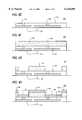
- This type of bonding processis also often referred to as "flip-chip", or "micro-bump” bonding. The process can be briefly explained with reference to FIGS. 1 and 2.
- FIG. 1shows a side view of a IC chip 10 and a module substrate 20.
- the IC chip 10is fabricated with various metal pattern lines and contacts 50 imprinted on its last metal level, as shown in FIG. 2.
- Formed beneath the IC chip 10is an array of solder balls 30.
- the module substrate 20includes metallized paths 60 for carrying signals from the IC chip 10 to other elements mounted on the substrate. These paths have contacts which match the contacts located on the underside of the IC chip 10.
- the IC chip 10When the IC chip 10 is ready to be mounted, it is placed on top of the module substrate 20 above the substrate contacts with the solder balls 30 attached to the contacts of the IC chip resting on the contacts of the module substrate, as shown in FIG. 1.
- FIG. 3shows the device after the solder has been heated and set.
- the completed moduleis then bonded to a mother board (not shown) through wire bonds or additional C4 connections at the module terminals.
- the contacts and solder ballshave been formed on the IC chip using metal mask technology.
- a metal maskessentially a metal plate with a pattern of holes therein
- contact material and solderare evaporated through the holes onto the wafer.
- the holes in the metal masksmust be of sufficient size to prevent warpage and damage of the mask during use.
- the number of contacts that can be fabricated through use of a metal maskis limited because the holes in the mask must remain above a minimum size to prevent these problems. Consequently, the size of the solder balls that can be created is similarly limited.
- the minimum diameter of a C4 solder ball that can be achieved using current techniques, such as metal mask,is approximately 100 microns. Since the size of the solder balls is directly related to the number and density of I/O terminals that can be fabricated on a given IC chip, a decrease in solder ball size would provide for an increase in the number and density of the I/O terminals. This would, in turn, allow for a significant increase in data transmission rates because of the increased number of I/O ports for the packaged IC circuit.
- the present inventionprovides an improved method for forming solder balls used in a C4 bonding process.
- the present inventorhas discovered that by using a tape liftoff process to form the solder contacts, significantly smaller contacts can be easily formed on an IC chip.
- the inventionis a method of fabricating contact terminals and solder balls on an IC chip.
- the fabricationutilizes a tape liftoff process to remove unwanted solder and photoresist.
- Use of the tape liftoff processallows formation of solder balls which are at least two orders of magnitude smaller than prior art solder balls.
- FIG. 1shows a cross-sectional view of a prior art integrated circuit package before C4 bonds are created.
- FIG. 2shows a top view of a prior art integrated circuit package before C4 bonds are created.
- FIG. 3shows a cross-sectional view of a prior art integrated circuit package after the C4 bonds are created.
- FIGS. 4A-4Qshow cross-sectional views of a structure fabricated in accordance with the method of the present invention.
- FIGS. 5A-5Eshow cross-sectional views of a structure fabricated in accordance with another method of the present invention.
- the present inventorhas discovered that by using a tape liftoff process for screening solder balls onto a substrate, the size of the solder balls can be significantly decreased.
- the process described belowcan be used to deposit solder balls on an IC chip, a module substrate, a circuit board, or any similar substrate.
- Tape liftoff processesper se, are known in the art, as evidenced by U.S. Pat. No. 5,240,878 to Fitzsimmons, which is incorporated herein by reference. Tape liftoff processes are frequently used to remove unwanted photoresist levels once an imaging and etching has taken place.
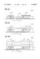
- FIGS. 4A-4Qillustrate the inventive process steps used to create micro solder balls on an IC wafer 110.
- FIG. 4Ashows the first stage in the formation of the micro solder balls on the wafer 110.
- an insulating layer 120such as silicon dioxide (SiO 2 )
- SiO 2silicon dioxide
- CVDchemical vapor deposition
- silicon dioxideis preferred for the first insulating layer
- other insulatorse.g., polyimide, silicon nitride, flourinated silicon dioxide
- the insulating layer 120should be applied so that its thickness is at least 2 microns greater than the thickness of the next to last metal layer 130. Then, the structure 100 is planarized using a chemical mechanical polishing process (CMP). The resulting device, after polishing, is as shown in FIG. 4B, where the excess insulating material has been smoothed away.
- CMPchemical mechanical polishing process
- a first layer of photoresist 125is deposited over the insulating layer 120.
- This photoresist layer 125may be made of any type of photoresist known to those skilled in the art.
- the photoresist layer 125is patterned and exposed to create via holes 140, as shown in FIG. 4D.
- the via holes 140are then used to etch into and remove portions of the insulating layer 120.
- FIG. 4Eshows the device after the photoresist layer 125 has been exposed, the via holes 140 have been etched, and the photoresist layer 125 has been removed. These via holes 140 provide a connection for upper conductive levels to the next to last layer of metallurgy 130.
- solderable metal pads 150are formed on the upper surface of the insulating layer 120. This is accomplished by depositing a second photoresist layer 145 on the planarized insulating layer 120, which will be used as a first liftoff layer.
- FIG. 4Fshows the device 100 after the photoresist layer 145 has been placed over the insulating layer 120.
- An insulatorsuch as polyimide may also be used in place of the photoresist layer 145, but it has been found that photoresist provides the best results in the present invention.
- This photoresist layer 145should be approximately 1.5 microns thick.
- the photoresist layer 145is patterned and etched down to the insulating layer 120 leaving exposed those areas on layer 120 where the metal pads 150 are desired, as shown in FIG. 4G. Then, a metal stack consisting of Zirconium (Zr), Nickel (Ni), Copper (Cu), and Gold (Au) is formed overtop of the entire device 100 including over the remaining areas of photoresist layer 145 and in the etched areas. This stack is formed by applying the four different metals, one at a time. Such a process is known in the art and described in U.S. Pat. Nos. 5,719,090 and 5,457,345, both to Cook et al., which are incorporated herein by reference.
- the Gold layeris optional in the metal stack, but provides excellent protection against oxidation.
- the thicknesses of each layer of metalis preferably approximately: 500 Angstroms of Zr, 750 Angstroms of Ni, 5000 Angstroms of Cu, and 750 Angstroms of Au, although these thicknesses are not critical. These metal layers are deposited to form metal stacks 150 in the etched areas of the photoresist layer 145, and to form excess metal stacks 150' on top of the photoresist layer 145.
- FIG. 4Hshows the device 100 after all metal layers have been deposited.
- the excess metal areas 150' which lie overtop of the photoresist layer 145,must now be removed. This is accomplished by a liftoff process.
- Liftoff processesare a well known method for removing unwanted portions of a device under fabrication. The present inventor has found that a tape-assisted liftoff process is especially beneficial in the disclosed process.
- the tape utilizedis an adhesive-backed polymer, which is applied overtop of the entire metallized resist layer, so that it contacts metal stacks 150'.
- the tapebonds to the metal stacks 150', which is, in turn, bonded to the photoresist layer 145.
- the removal of the tapecauses all of the metal 150' and photoresist 145 to be stripped away, leaving metal pads 150 in only those areas which were previously etched in the photoresist layer 145.
- the resulting device 100 after the tape liftoffappears as shown in FIG. 41.
- a second insulating layer 160is added overtop of the device 100, as shown in FIG. 4J.
- This insulating layer 160can be formed of conventional insulating material, such as polyimide, and should be approximately 1.5 microns thick. Although polyimide is preferred for this layer, any insulator known to those skilled in the art may be used (e.g., silicon dioxide, silicon nitride, flourinated silicon dioxide).
- FIG. 4Kshows the next step where a third photoresist layer 170 is deposited for use as a second liftoff layer.
- This photoresist layer 170can be a continuous layer of photoresist as shown in FIG. 4K, or can alternatively comprise a ⁇ hard mask ⁇ layer.
- the ⁇ hard mask ⁇ designis shown in FIG. 4Q, where a 500 Angstrom layer of silicon nitride (Si 3 N 4 ) 175 is sandwiched between two photoresist layers 176 and 177.
- the upper most photoresist layerwill be approximately 0.5 microns thick, with the underlying photoresist layer being thick enough so that the entire stack (i.e. layers 175-177) is thicker than the layer of solder which will be subsequently deposited.
- the lower level of photoresist 177is approximately 0.5 microns thick.
- the photoresistmust be at least as thick as the layer of solder which will be subsequently applied (i.e. approximately 3 microns).
- the photoresist layers 176, 177need not be that thick, as long as the entire stack is thicker than layer of solder to be applied.
- the second photoresist layer 170may alternatively comprise a peel-away insulator, such as photosensitive polyimide.
- the second photoresist layer 170is exposed and patterned to produce through holes 180 in the areas above the metal pads 150. Then, the insulator 160 is etched through the holes 180 so that the metal pads 150 are exposed, as shown in FIG. 4M.
- solder 190is deposited over the entire device 100.
- the soldershould be deposited so that it is at least 2.33 microns thick. This process produces solder contacts 200 in the through holes 180.
- the photoresist layer 170 and the solder layer 190are removed using the tape liftoff process described above with reference to photoresist layer 145.
- the solder layer 190 and the photoresist layer 170are lifted away from the insulating layer 160 by an adhesive tape which is applied overtop of the solder layer 190.
- the tapeis an adhesive backed polymer which is applied to the solder layer 190 and subsequently stripped off to remove the unwanted solder 190 and photoresist 170 layers. Since the solder layer 190 will bond to the photoresist layer 170, the stripping action causes both layers (i.e. 170 and 190) to be removed simultaneously.
- FIG. 4Oshows the device 100 after the unwanted photoresist and solder have been removed.
- Solder contacts 200which connect with metal pads 150 now project out of the top surface of insulating layer 160.
- the solder contacts 200are heated to allow them to reflow.
- solder ball contacts 210are composite contacts, including both the flat contact portion and the solder ball portion in a single unit.
- a single liftoff procedureis used to form both the metal pads 150 and the solder ball contacts 200, instead of the multiple liftoff procedure descibed above.
- This embodimentis useful where only contact pads are to be formed in the last metal layer 130 (i.e. the pad metallurgy). This alternate process will now be explained with reference to FIGS. 4(E) and 5(A-E).
- step 4(E)instead of depositing a photoresist layer 145 (shown in FIG. 4(F)), a thicker photoresist layer 300 is applied overtop of the entire surface of the device 100 (See FIG. 5(A)). Then, as shown in FIG. 5(B), holes 310 are formed in the photoresist 300. These holes 310 are selected according to the desired size of the solder ball contact (i.e. the larger the holes 310, the larger the diameter of the solder ball contact). As shown in FIG. 5(C), the metal pads 320 (150 in FIG. 4(H)) and the solder ball contacts 330 (200 in FIG. 4(O)) are deposited in the holes 310 formed in the photoresist 300 in a single step.
- the metal pads 320comprising the layers of Zr, Ni, Cu, and Au are deposited by the process described above with reference to FIG. 4(H). Then, a layer of solder 330 is deposited. The ensuing liftoff process remove all the excess solder and pad metal to create a device like the one shown in FIG. 5(D).
- the stack 340 which is formedis a composite stack, with the four-layer metal pad on the bottom and solder on the top. The entire stack 340 is then reflowed to form the solder ball contacts 350 shown in FIG. 5(E).
- solder ball contacts in the inventionare formed by deposition of solder through fine closely spaced holes in a photoresist layer and by using a tape liftoff process, rather than a metal mask process, the size of the contacts is decreased significantly.
- Solder contacts formed using the above processare approximately 2 microns in diameter. This is a significant improvement over prior art solder ball contacts, which are currently 100 microns in diameter.
- the above processcan be used to form solder contacts which are approximately 2 microns in diameter, it can also be used by those skilled in the art to produce solder contacts of any size, but particularly those in the range of 2 microns to 100 microns.
- solder contacts10 25, 50 or 75 microns, or any other size in the range of 2 to 100 microns, or in a narrower range such as less than 50 microns, or less than 25 microns, or less than 10 microns, as non-limiting examples.
- the waferWhen producing multiple chips on a wafer, the wafer can be diced, after the solder ball contacts 210 are formed over the entire wafer, to create a multitude of chips with solder ball contacts 210. These individual chips can then be attached to a module substrate or circuit board using the C4 process described above with reference to FIGS. 1-3.
- solder contactshave been described and illustrated with respect to forming solder contacts on an integrated circuit chip, it should be apparent that the same processing techniques can be used to form solder contacts on a module substrate, a printed circuit board or other conductor bearing substrate.
Landscapes
- Engineering & Computer Science (AREA)
- Computer Hardware Design (AREA)
- Microelectronics & Electronic Packaging (AREA)
- Power Engineering (AREA)
- Manufacturing & Machinery (AREA)
- Ceramic Engineering (AREA)
- Physics & Mathematics (AREA)
- Condensed Matter Physics & Semiconductors (AREA)
- General Physics & Mathematics (AREA)
- Internal Circuitry In Semiconductor Integrated Circuit Devices (AREA)
Abstract
Description
Claims (47)
Priority Applications (3)
| Application Number | Priority Date | Filing Date | Title |
|---|---|---|---|
| US09/134,363US6136689A (en) | 1998-08-14 | 1998-08-14 | Method of forming a micro solder ball for use in C4 bonding process |
| US09/638,026US6998711B1 (en) | 1998-08-14 | 2000-08-14 | Method of forming a micro solder ball for use in C4 bonding process |
| US11/219,751US20060006544A1 (en) | 1998-08-14 | 2005-09-07 | Method of forming a micro solder ball for use in C4 bonding process |
Applications Claiming Priority (1)
| Application Number | Priority Date | Filing Date | Title |
|---|---|---|---|
| US09/134,363US6136689A (en) | 1998-08-14 | 1998-08-14 | Method of forming a micro solder ball for use in C4 bonding process |
Related Child Applications (1)
| Application Number | Title | Priority Date | Filing Date |
|---|---|---|---|
| US09/638,026DivisionUS6998711B1 (en) | 1998-08-14 | 2000-08-14 | Method of forming a micro solder ball for use in C4 bonding process |
Publications (1)
| Publication Number | Publication Date |
|---|---|
| US6136689Atrue US6136689A (en) | 2000-10-24 |
Family
ID=22463033
Family Applications (1)
| Application Number | Title | Priority Date | Filing Date |
|---|---|---|---|
| US09/134,363Expired - LifetimeUS6136689A (en) | 1998-08-14 | 1998-08-14 | Method of forming a micro solder ball for use in C4 bonding process |
Country Status (1)
| Country | Link |
|---|---|
| US (1) | US6136689A (en) |
Cited By (19)
| Publication number | Priority date | Publication date | Assignee | Title |
|---|---|---|---|---|
| US20020034581A1 (en)* | 2000-04-10 | 2002-03-21 | Farrar Paul A. | Micro C-4 semiconductor die and method for depositing connection sites thereon |
| US6518667B1 (en)* | 2000-02-29 | 2003-02-11 | Allied Material Corporation | Semiconductor package using micro balls and production method thereof |
| US6552424B2 (en) | 2001-08-30 | 2003-04-22 | Micron Technology, Inc. | Angled edge connections for multichip structures |
| US20050046034A1 (en)* | 2003-09-03 | 2005-03-03 | Micron Technology, Inc. | Apparatus and method for high density multi-chip structures |
| US20050133572A1 (en)* | 2003-12-22 | 2005-06-23 | Rohm And Haas Electronic Materials Llc | Methods of forming solder areas on electronic components and electronic components having solder areas |
| US20050139644A1 (en)* | 2003-12-22 | 2005-06-30 | Rohm And Haas Electronic Materials Llc | Electronic devices and methods of forming electronic devices |
| US20060001141A1 (en)* | 2002-08-29 | 2006-01-05 | Micron Technology, Inc. | Multi-component integrated circuit contacts |
| US20060022017A1 (en)* | 2003-06-24 | 2006-02-02 | Micron Technology, Inc. | Apparatus and method for printing micro metal structures |
| US20060124699A1 (en)* | 2000-02-04 | 2006-06-15 | Farrar Paul A | Micro-C-4 semiconductor die and method for depositing connection sites thereon |
| US20070116605A1 (en)* | 2003-02-18 | 2007-05-24 | Intel Corporation | Methods for uniform metal impregnation into a nanoporous material |
| US20070193023A1 (en)* | 2006-02-17 | 2007-08-23 | Fujitsu Limited | Method of manufacturing magnetic head |
| US20070269935A1 (en)* | 2006-05-18 | 2007-11-22 | Rajiv Pethe | Fabrication of conductive micro traces using a deform and selective removal process |
| US20080054489A1 (en)* | 2006-08-31 | 2008-03-06 | Micron Technology, Inc. | Distributed semiconductor device methods, apparatus, and systems |
| US20080096320A1 (en)* | 2006-10-19 | 2008-04-24 | Micron Technology, Inc. | High density chip packages, methods of forming, and systems including same |
| US20090090950A1 (en)* | 2007-10-05 | 2009-04-09 | Micron Technology, Inc. | Semiconductor devices |
| US20090127592A1 (en)* | 2007-11-19 | 2009-05-21 | Micron Technology, Inc. | Fin-jfet |
| US20100062600A1 (en)* | 2008-09-08 | 2010-03-11 | Oki Semiconductor Co., Ltd. | Method of manufacturing a semiconductor device |
| US20110222345A1 (en)* | 2005-03-16 | 2011-09-15 | Yan Li | Non-Volatile Memory and Method With Power-Saving Read and Program-Verify Operations |
| CN113193094A (en)* | 2021-04-27 | 2021-07-30 | 成都辰显光电有限公司 | Batch transfer method and display panel |
Citations (9)
| Publication number | Priority date | Publication date | Assignee | Title |
|---|---|---|---|---|
| US4532002A (en)* | 1984-04-10 | 1985-07-30 | Rca Corporation | Multilayer planarizing structure for lift-off technique |
| US4606998A (en)* | 1985-04-30 | 1986-08-19 | International Business Machines Corporation | Barrierless high-temperature lift-off process |
| US5457345A (en)* | 1992-05-11 | 1995-10-10 | International Business Machines Corporation | Metallization composite having nickle intermediate/interface |
| US5667132A (en)* | 1996-04-19 | 1997-09-16 | Lucent Technologies Inc. | Method for solder-bonding contact pad arrays |
| US5691239A (en)* | 1994-11-22 | 1997-11-25 | International Business Machines Corporation | Method for fabricating an electrical connect above an integrated circuit |
| US5762259A (en)* | 1995-07-13 | 1998-06-09 | Motorola Inc. | Method for forming bumps on a substrate |
| US5786270A (en)* | 1996-05-29 | 1998-07-28 | W. L. Gore & Associates, Inc. | Method of forming raised metallic contacts on electrical circuits for permanent bonding |
| US5838069A (en)* | 1996-04-11 | 1998-11-17 | Ngk Spark Plug Co., Ltd. | Ceramic substrate having pads to be attached to terminal members with Pb-Sn solder and method of producing the same |
| US5866475A (en)* | 1996-05-08 | 1999-02-02 | Sony Corporation | Method of forming solder bumps |
- 1998
- 1998-08-14USUS09/134,363patent/US6136689A/ennot_activeExpired - Lifetime
Patent Citations (9)
| Publication number | Priority date | Publication date | Assignee | Title |
|---|---|---|---|---|
| US4532002A (en)* | 1984-04-10 | 1985-07-30 | Rca Corporation | Multilayer planarizing structure for lift-off technique |
| US4606998A (en)* | 1985-04-30 | 1986-08-19 | International Business Machines Corporation | Barrierless high-temperature lift-off process |
| US5457345A (en)* | 1992-05-11 | 1995-10-10 | International Business Machines Corporation | Metallization composite having nickle intermediate/interface |
| US5691239A (en)* | 1994-11-22 | 1997-11-25 | International Business Machines Corporation | Method for fabricating an electrical connect above an integrated circuit |
| US5762259A (en)* | 1995-07-13 | 1998-06-09 | Motorola Inc. | Method for forming bumps on a substrate |
| US5838069A (en)* | 1996-04-11 | 1998-11-17 | Ngk Spark Plug Co., Ltd. | Ceramic substrate having pads to be attached to terminal members with Pb-Sn solder and method of producing the same |
| US5667132A (en)* | 1996-04-19 | 1997-09-16 | Lucent Technologies Inc. | Method for solder-bonding contact pad arrays |
| US5866475A (en)* | 1996-05-08 | 1999-02-02 | Sony Corporation | Method of forming solder bumps |
| US5786270A (en)* | 1996-05-29 | 1998-07-28 | W. L. Gore & Associates, Inc. | Method of forming raised metallic contacts on electrical circuits for permanent bonding |
Non-Patent Citations (2)
| Title |
|---|
| Soller et al., A flexible multi layer resist system using low temperature plasma deposited silicon nitride, Journal of the Electrochemical society, vol. 131, No. 4 p. 868 72, Apr. 1984.* |
| Soller et al., A flexible multi-layer resist system using low temperature plasma-deposited silicon nitride, Journal of the Electrochemical society, vol. 131, No. 4 p. 868-72, Apr. 1984. |
Cited By (56)
| Publication number | Priority date | Publication date | Assignee | Title |
|---|---|---|---|---|
| US20060124699A1 (en)* | 2000-02-04 | 2006-06-15 | Farrar Paul A | Micro-C-4 semiconductor die and method for depositing connection sites thereon |
| US6518667B1 (en)* | 2000-02-29 | 2003-02-11 | Allied Material Corporation | Semiconductor package using micro balls and production method thereof |
| US7028879B2 (en) | 2000-04-10 | 2006-04-18 | Micron Technology, Inc. | System for depositing connection sites on micro C-4 semiconductor die |
| US6958287B2 (en)* | 2000-04-10 | 2005-10-25 | Micron Technology, Inc. | Micro C-4 semiconductor die |
| US20030186485A1 (en)* | 2000-04-10 | 2003-10-02 | Farrar Paul A. | Micro C-4 semiconductor die and method for depositing connection sites thereon |
| US6878396B2 (en)* | 2000-04-10 | 2005-04-12 | Micron Technology, Inc. | Micro C-4 semiconductor die and method for depositing connection sites thereon |
| US20020034581A1 (en)* | 2000-04-10 | 2002-03-21 | Farrar Paul A. | Micro C-4 semiconductor die and method for depositing connection sites thereon |
| US6635960B2 (en) | 2001-08-30 | 2003-10-21 | Micron Technology, Inc. | Angled edge connections for multichip structures |
| US6552424B2 (en) | 2001-08-30 | 2003-04-22 | Micron Technology, Inc. | Angled edge connections for multichip structures |
| US6591492B2 (en) | 2001-08-30 | 2003-07-15 | Micron Technology, Inc. | Angled edge connections for multichip structures |
| US20060001141A1 (en)* | 2002-08-29 | 2006-01-05 | Micron Technology, Inc. | Multi-component integrated circuit contacts |
| US20100203721A1 (en)* | 2002-08-29 | 2010-08-12 | Hiatt William M | Multi-component integrated circuit contacts |
| US7446028B2 (en)* | 2002-08-29 | 2008-11-04 | Micron Technology, Inc. | Multi-component integrated circuit contacts |
| US7719120B2 (en) | 2002-08-29 | 2010-05-18 | Micron Technology, Inc. | Multi-component integrated circuit contacts |
| US8268715B2 (en)* | 2002-08-29 | 2012-09-18 | Micron Technology, Inc. | Multi-component integrated circuit contacts |
| US20070018321A1 (en)* | 2002-08-29 | 2007-01-25 | Micron Technology, Inc. | Multi-component integrated circuit contacts |
| US9337162B2 (en) | 2002-08-29 | 2016-05-10 | Micron Technology, Inc. | Multi-component integrated circuit contacts |
| US20070116605A1 (en)* | 2003-02-18 | 2007-05-24 | Intel Corporation | Methods for uniform metal impregnation into a nanoporous material |
| US20060022017A1 (en)* | 2003-06-24 | 2006-02-02 | Micron Technology, Inc. | Apparatus and method for printing micro metal structures |
| US20060032890A1 (en)* | 2003-06-24 | 2006-02-16 | Micron Technology, Inc. | Apparatus and method for printing micro metal structures |
| US7322511B2 (en) | 2003-06-24 | 2008-01-29 | Micron Technology, Inc. | Apparatus and method for printing micro metal structures |
| US7347349B2 (en) | 2003-06-24 | 2008-03-25 | Micron Technology, Inc. | Apparatus and method for printing micro metal structures |
| US20060063302A1 (en)* | 2003-09-03 | 2006-03-23 | Micron Technology, Inc. | Apparatus and method for high density multi-chip structures |
| US8592964B2 (en) | 2003-09-03 | 2013-11-26 | Micron Technology, Inc. | Apparatus and method for high density multi-chip structures |
| US9209127B2 (en) | 2003-09-03 | 2015-12-08 | Micron Technology | Apparatus and method for high density multi-chip structures |
| US20060289990A1 (en)* | 2003-09-03 | 2006-12-28 | Micron Technology, Inc. | Apparatus and method for high density multi-chip structures |
| US7560305B2 (en) | 2003-09-03 | 2009-07-14 | Micron Technology, Inc. | Apparatus and method for high density multi-chip structures |
| US20050046034A1 (en)* | 2003-09-03 | 2005-03-03 | Micron Technology, Inc. | Apparatus and method for high density multi-chip structures |
| US20050139644A1 (en)* | 2003-12-22 | 2005-06-30 | Rohm And Haas Electronic Materials Llc | Electronic devices and methods of forming electronic devices |
| US20050133572A1 (en)* | 2003-12-22 | 2005-06-23 | Rohm And Haas Electronic Materials Llc | Methods of forming solder areas on electronic components and electronic components having solder areas |
| US20110222345A1 (en)* | 2005-03-16 | 2011-09-15 | Yan Li | Non-Volatile Memory and Method With Power-Saving Read and Program-Verify Operations |
| US20070193023A1 (en)* | 2006-02-17 | 2007-08-23 | Fujitsu Limited | Method of manufacturing magnetic head |
| US7498183B2 (en)* | 2006-05-18 | 2009-03-03 | Southwall Technologies, Inc. | Fabrication of conductive micro traces using a deform and selective removal process |
| US20070269935A1 (en)* | 2006-05-18 | 2007-11-22 | Rajiv Pethe | Fabrication of conductive micro traces using a deform and selective removal process |
| US8872324B2 (en) | 2006-08-31 | 2014-10-28 | Micron Technology, Inc. | Distributed semiconductor device methods, apparatus, and systems |
| US8729691B2 (en) | 2006-08-31 | 2014-05-20 | Micron Technology, Inc. | Distributed semiconductor device methods, apparatus, and systems |
| US20080054489A1 (en)* | 2006-08-31 | 2008-03-06 | Micron Technology, Inc. | Distributed semiconductor device methods, apparatus, and systems |
| US8498171B2 (en) | 2006-08-31 | 2013-07-30 | Micron Technology, Inc. | Distributed semiconductor device methods, apparatus, and systems |
| US7952184B2 (en) | 2006-08-31 | 2011-05-31 | Micron Technology, Inc. | Distributed semiconductor device methods, apparatus, and systems |
| US8237254B2 (en) | 2006-08-31 | 2012-08-07 | Micron Technology, Inc. | Distributed semiconductor device methods, apparatus, and systems |
| US20110222328A1 (en)* | 2006-08-31 | 2011-09-15 | Farrar Paul A | Distributed semiconductor device methods, apparatus, and systems |
| US8841169B2 (en) | 2006-10-19 | 2014-09-23 | Micron Technology, Inc. | High density chip packages, methods of forming, and systems including same |
| US20100271777A1 (en)* | 2006-10-19 | 2010-10-28 | Farrar Paul A | High density chip packages, methods of forming, and systems including same |
| US20080096320A1 (en)* | 2006-10-19 | 2008-04-24 | Micron Technology, Inc. | High density chip packages, methods of forming, and systems including same |
| US8470642B2 (en) | 2006-10-19 | 2013-06-25 | Micron Technology, Inc. | High density chip packages, methods of forming, and systems including same |
| US7754532B2 (en) | 2006-10-19 | 2010-07-13 | Micron Technology, Inc. | High density chip packages, methods of forming, and systems including same |
| US20090090950A1 (en)* | 2007-10-05 | 2009-04-09 | Micron Technology, Inc. | Semiconductor devices |
| US7875529B2 (en) | 2007-10-05 | 2011-01-25 | Micron Technology, Inc. | Semiconductor devices |
| US7927938B2 (en) | 2007-11-19 | 2011-04-19 | Micron Technology, Inc. | Fin-JFET |
| US8502280B2 (en) | 2007-11-19 | 2013-08-06 | Micron Technology, Inc. | Fin-JFET |
| US9076662B2 (en) | 2007-11-19 | 2015-07-07 | Micron Technology, Inc. | Fin-JFET |
| US20110210379A1 (en)* | 2007-11-19 | 2011-09-01 | Micron Technology, Inc. | Fin-jfet |
| US20090127592A1 (en)* | 2007-11-19 | 2009-05-21 | Micron Technology, Inc. | Fin-jfet |
| US20100062600A1 (en)* | 2008-09-08 | 2010-03-11 | Oki Semiconductor Co., Ltd. | Method of manufacturing a semiconductor device |
| CN113193094A (en)* | 2021-04-27 | 2021-07-30 | 成都辰显光电有限公司 | Batch transfer method and display panel |
| CN113193094B (en)* | 2021-04-27 | 2023-03-21 | 成都辰显光电有限公司 | Batch transfer method and display panel |
Similar Documents
| Publication | Publication Date | Title |
|---|---|---|
| US6136689A (en) | Method of forming a micro solder ball for use in C4 bonding process | |
| CN100385642C (en) | Pad redistribution layer and method for fabricating copper pad redistribution layer | |
| US6998711B1 (en) | Method of forming a micro solder ball for use in C4 bonding process | |
| US6605525B2 (en) | Method for forming a wafer level package incorporating a multiplicity of elastomeric blocks and package formed | |
| US6825547B2 (en) | Semiconductor device including edge bond pads | |
| US6075712A (en) | Flip-chip having electrical contact pads on the backside of the chip | |
| US7329563B2 (en) | Method for fabrication of wafer level package incorporating dual compliant layers | |
| US5244833A (en) | Method for manufacturing an integrated circuit chip bump electrode using a polymer layer and a photoresist layer | |
| US6001493A (en) | Substrate for transferring bumps and method of use | |
| US5010389A (en) | Integrated circuit substrate with contacts thereon for a packaging structure | |
| US6433427B1 (en) | Wafer level package incorporating dual stress buffer layers for I/O redistribution and method for fabrication | |
| JP3285796B2 (en) | Conductive contact pad connection method | |
| US10032738B2 (en) | Method for forming bump of semiconductor package | |
| US6265300B1 (en) | Wire bonding surface and bonding method | |
| US6372619B1 (en) | Method for fabricating wafer level chip scale package with discrete package encapsulation | |
| US6914333B2 (en) | Wafer level package incorporating dual compliant layers and method for fabrication | |
| US6228689B1 (en) | Trench style bump and application of the same | |
| US6583039B2 (en) | Method of forming a bump on a copper pad | |
| US7141885B2 (en) | Wafer level package with air pads and manufacturing method thereof | |
| US7009300B2 (en) | Low profile stacked multi-chip package and method of forming same | |
| US6767818B1 (en) | Method for forming electrically conductive bumps and devices formed | |
| US20090032940A1 (en) | Conductor Bump Method and Apparatus | |
| US20050258536A1 (en) | Chip heat sink device and method | |
| TWI854732B (en) | Interconnecting structure with high aspect ratio tsv and method for forming the same | |
| JP3424164B2 (en) | Manufacturing method of semiconductor device |
Legal Events
| Date | Code | Title | Description |
|---|---|---|---|
| AS | Assignment | Owner name:MICRON TECHNOLOGY, INC., IDAHO Free format text:ASSIGNMENT OF ASSIGNORS INTEREST;ASSIGNOR:FARRAR, PAUL A.;REEL/FRAME:009393/0956 Effective date:19980811 | |
| STCF | Information on status: patent grant | Free format text:PATENTED CASE | |
| FPAY | Fee payment | Year of fee payment:4 | |
| FEPP | Fee payment procedure | Free format text:PAYOR NUMBER ASSIGNED (ORIGINAL EVENT CODE: ASPN); ENTITY STATUS OF PATENT OWNER: LARGE ENTITY | |
| FPAY | Fee payment | Year of fee payment:8 | |
| FPAY | Fee payment | Year of fee payment:12 | |
| AS | Assignment | Owner name:U.S. BANK NATIONAL ASSOCIATION, AS COLLATERAL AGENT, CALIFORNIA Free format text:SECURITY INTEREST;ASSIGNOR:MICRON TECHNOLOGY, INC.;REEL/FRAME:038669/0001 Effective date:20160426 Owner name:U.S. BANK NATIONAL ASSOCIATION, AS COLLATERAL AGEN Free format text:SECURITY INTEREST;ASSIGNOR:MICRON TECHNOLOGY, INC.;REEL/FRAME:038669/0001 Effective date:20160426 | |
| AS | Assignment | Owner name:MORGAN STANLEY SENIOR FUNDING, INC., AS COLLATERAL AGENT, MARYLAND Free format text:PATENT SECURITY AGREEMENT;ASSIGNOR:MICRON TECHNOLOGY, INC.;REEL/FRAME:038954/0001 Effective date:20160426 Owner name:MORGAN STANLEY SENIOR FUNDING, INC., AS COLLATERAL Free format text:PATENT SECURITY AGREEMENT;ASSIGNOR:MICRON TECHNOLOGY, INC.;REEL/FRAME:038954/0001 Effective date:20160426 | |
| AS | Assignment | Owner name:U.S. BANK NATIONAL ASSOCIATION, AS COLLATERAL AGENT, CALIFORNIA Free format text:CORRECTIVE ASSIGNMENT TO CORRECT THE REPLACE ERRONEOUSLY FILED PATENT #7358718 WITH THE CORRECT PATENT #7358178 PREVIOUSLY RECORDED ON REEL 038669 FRAME 0001. ASSIGNOR(S) HEREBY CONFIRMS THE SECURITY INTEREST;ASSIGNOR:MICRON TECHNOLOGY, INC.;REEL/FRAME:043079/0001 Effective date:20160426 Owner name:U.S. BANK NATIONAL ASSOCIATION, AS COLLATERAL AGEN Free format text:CORRECTIVE ASSIGNMENT TO CORRECT THE REPLACE ERRONEOUSLY FILED PATENT #7358718 WITH THE CORRECT PATENT #7358178 PREVIOUSLY RECORDED ON REEL 038669 FRAME 0001. ASSIGNOR(S) HEREBY CONFIRMS THE SECURITY INTEREST;ASSIGNOR:MICRON TECHNOLOGY, INC.;REEL/FRAME:043079/0001 Effective date:20160426 | |
| AS | Assignment | Owner name:JPMORGAN CHASE BANK, N.A., AS COLLATERAL AGENT, ILLINOIS Free format text:SECURITY INTEREST;ASSIGNORS:MICRON TECHNOLOGY, INC.;MICRON SEMICONDUCTOR PRODUCTS, INC.;REEL/FRAME:047540/0001 Effective date:20180703 Owner name:JPMORGAN CHASE BANK, N.A., AS COLLATERAL AGENT, IL Free format text:SECURITY INTEREST;ASSIGNORS:MICRON TECHNOLOGY, INC.;MICRON SEMICONDUCTOR PRODUCTS, INC.;REEL/FRAME:047540/0001 Effective date:20180703 | |
| AS | Assignment | Owner name:MICRON TECHNOLOGY, INC., IDAHO Free format text:RELEASE BY SECURED PARTY;ASSIGNOR:U.S. BANK NATIONAL ASSOCIATION, AS COLLATERAL AGENT;REEL/FRAME:047243/0001 Effective date:20180629 | |
| AS | Assignment | Owner name:MICRON TECHNOLOGY, INC., IDAHO Free format text:RELEASE BY SECURED PARTY;ASSIGNOR:MORGAN STANLEY SENIOR FUNDING, INC., AS COLLATERAL AGENT;REEL/FRAME:050937/0001 Effective date:20190731 | |
| AS | Assignment | Owner name:MICRON TECHNOLOGY, INC., IDAHO Free format text:RELEASE BY SECURED PARTY;ASSIGNOR:JPMORGAN CHASE BANK, N.A., AS COLLATERAL AGENT;REEL/FRAME:051028/0001 Effective date:20190731 Owner name:MICRON SEMICONDUCTOR PRODUCTS, INC., IDAHO Free format text:RELEASE BY SECURED PARTY;ASSIGNOR:JPMORGAN CHASE BANK, N.A., AS COLLATERAL AGENT;REEL/FRAME:051028/0001 Effective date:20190731 |