US6135863A - Method of conditioning wafer polishing pads - Google Patents
Method of conditioning wafer polishing padsDownload PDFInfo
- Publication number
- US6135863A US6135863AUS09/295,127US29512799AUS6135863AUS 6135863 AUS6135863 AUS 6135863AUS 29512799 AUS29512799 AUS 29512799AUS 6135863 AUS6135863 AUS 6135863A
- Authority
- US
- United States
- Prior art keywords
- polishing
- conditioning
- pad
- cycle
- machine
- Prior art date
- Legal status (The legal status is an assumption and is not a legal conclusion. Google has not performed a legal analysis and makes no representation as to the accuracy of the status listed.)
- Expired - Fee Related
Links
- 238000005498polishingMethods0.000titleclaimsabstractdescription226
- 238000000034methodMethods0.000titleclaimsabstractdescription70
- 230000003750conditioning effectEffects0.000titleclaimsabstractdescription51
- 235000012431wafersNutrition0.000claimsabstractdescription106
- 239000002002slurrySubstances0.000claimsabstractdescription39
- 230000001143conditioned effectEffects0.000claimsabstractdescription21
- 239000004065semiconductorSubstances0.000claimsabstractdescription18
- 239000011148porous materialSubstances0.000claimsabstractdescription7
- 239000002245particleSubstances0.000claimsdescription9
- 239000000463materialSubstances0.000claimsdescription6
- HBMJWWWQQXIZIP-UHFFFAOYSA-Nsilicon carbideChemical compound[Si+]#[C-]HBMJWWWQQXIZIP-UHFFFAOYSA-N0.000claimsdescription2
- 229910010271silicon carbideInorganic materials0.000claimsdescription2
- 229910010293ceramic materialInorganic materials0.000claims1
- 239000003082abrasive agentSubstances0.000abstract1
- 239000000969carrierSubstances0.000description23
- VYPSYNLAJGMNEJ-UHFFFAOYSA-NSilicium dioxideChemical compoundO=[Si]=OVYPSYNLAJGMNEJ-UHFFFAOYSA-N0.000description12
- 239000000377silicon dioxideSubstances0.000description5
- 238000000227grindingMethods0.000description4
- 238000010586diagramMethods0.000description3
- 238000005259measurementMethods0.000description3
- 229920000728polyesterPolymers0.000description3
- 229920002635polyurethanePolymers0.000description3
- 239000004814polyurethaneSubstances0.000description3
- 239000008119colloidal silicaSubstances0.000description2
- 238000010276constructionMethods0.000description2
- 239000013078crystalSubstances0.000description2
- 229910021421monocrystalline siliconInorganic materials0.000description2
- 239000000126substanceSubstances0.000description2
- 229910001018Cast ironInorganic materials0.000description1
- 229920004943Delrin®Polymers0.000description1
- XUIMIQQOPSSXEZ-UHFFFAOYSA-NSiliconChemical compound[Si]XUIMIQQOPSSXEZ-UHFFFAOYSA-N0.000description1
- 229920001070TechronPolymers0.000description1
- 239000000919ceramicSubstances0.000description1
- 239000003795chemical substances by applicationSubstances0.000description1
- 230000006835compressionEffects0.000description1
- 238000007906compressionMethods0.000description1
- 238000001816coolingMethods0.000description1
- 239000000498cooling waterSubstances0.000description1
- 238000005520cutting processMethods0.000description1
- 230000007423decreaseEffects0.000description1
- 230000007547defectEffects0.000description1
- 230000007812deficiencyEffects0.000description1
- 238000005530etchingMethods0.000description1
- 238000009434installationMethods0.000description1
- 238000004519manufacturing processMethods0.000description1
- 229920003023plasticPolymers0.000description1
- 239000004033plasticSubstances0.000description1
- 238000007517polishing processMethods0.000description1
- 238000002360preparation methodMethods0.000description1
- 238000010008shearingMethods0.000description1
- 229910052710siliconInorganic materials0.000description1
- 239000010703siliconSubstances0.000description1
Images


Classifications
- H—ELECTRICITY
- H01—ELECTRIC ELEMENTS
- H01L—SEMICONDUCTOR DEVICES NOT COVERED BY CLASS H10
- H01L21/00—Processes or apparatus adapted for the manufacture or treatment of semiconductor or solid state devices or of parts thereof
- H01L21/02—Manufacture or treatment of semiconductor devices or of parts thereof
- H01L21/04—Manufacture or treatment of semiconductor devices or of parts thereof the devices having potential barriers, e.g. a PN junction, depletion layer or carrier concentration layer
- H01L21/18—Manufacture or treatment of semiconductor devices or of parts thereof the devices having potential barriers, e.g. a PN junction, depletion layer or carrier concentration layer the devices having semiconductor bodies comprising elements of Group IV of the Periodic Table or AIIIBV compounds with or without impurities, e.g. doping materials
- H01L21/30—Treatment of semiconductor bodies using processes or apparatus not provided for in groups H01L21/20 - H01L21/26
- H01L21/302—Treatment of semiconductor bodies using processes or apparatus not provided for in groups H01L21/20 - H01L21/26 to change their surface-physical characteristics or shape, e.g. etching, polishing, cutting
- B—PERFORMING OPERATIONS; TRANSPORTING
- B24—GRINDING; POLISHING
- B24B—MACHINES, DEVICES, OR PROCESSES FOR GRINDING OR POLISHING; DRESSING OR CONDITIONING OF ABRADING SURFACES; FEEDING OF GRINDING, POLISHING, OR LAPPING AGENTS
- B24B53/00—Devices or means for dressing or conditioning abrasive surfaces
- B24B53/017—Devices or means for dressing, cleaning or otherwise conditioning lapping tools
- B—PERFORMING OPERATIONS; TRANSPORTING
- B24—GRINDING; POLISHING
- B24B—MACHINES, DEVICES, OR PROCESSES FOR GRINDING OR POLISHING; DRESSING OR CONDITIONING OF ABRADING SURFACES; FEEDING OF GRINDING, POLISHING, OR LAPPING AGENTS
- B24B57/00—Devices for feeding, applying, grading or recovering grinding, polishing or lapping agents
- B24B57/02—Devices for feeding, applying, grading or recovering grinding, polishing or lapping agents for feeding of fluid, sprayed, pulverised, or liquefied grinding, polishing or lapping agents
Definitions
- This inventionrelates generally to wafer polishing and, particularly, to a method of conditioning a pad for use in polishing semiconductor wafers with a double side or single side polishing machine.
- Semiconductor wafersare produced by thinly slicing a single crystal ingot into individual wafers with a cutting apparatus, such as a wire saw or inner diameter saw.
- the as-cut wafersundergo a number of processing operations to shape them, reduce their thicknesses and remove damage caused by the slicing operation.
- the wafersundergo chemical-mechanical polishing to planarize their surfaces. This polishing technique involves rubbing each wafer with a polishing pad in a solution that contains an abrasive and chemicals to produce an extremely flat, highly reflective and damage-free wafer surface.
- polishing solutionincludes a colloidal silica and an alkaline etchant.
- the polishing padis, for example, a polyurethane impregnated polyester felt having a thickness between about 1.5 mm and 2.0 mm.
- the flatness of the waferis a critical parameter to customers since it has a direct impact on the subsequent use and quality of semiconductor chips diced from the wafer.
- a number of parametersdetermine the wafer flatness, including a GBIR (Global Backside Indicated Reading) measurement.
- the GBIR measurementrepresents the difference between the highest point on a top surface of the wafer with respect to a reference plane parallel to the back side of the wafer.
- the waferis mounted on a vacuum chuck that translates any surface variations on the back side of the wafer to the front side of the wafer for measurement.
- ADE Corporation of Westwood, Mass.sells non-contacting electric-capacity type sensors for characterizing wafer geometry and measuring flatness under the trademarks UltraGage® 9500 and Galaxy AFS-300TM.
- a polishing machinepolishes many wafers simultaneously.
- Such a machinetypically holds 5 to 30 wafers, depending on their size, in carriers.
- the machinemoves the carriers relative to a rotating circular turntable, or platen, for polishing.
- the platenis typically cast iron and overlaid with a polishing pad.
- the machinedispenses a stream of polishing slurry to a surface of the pad while the pad is pressed against the wafers.
- Single-side polishing machineshave one platen for polishing a surface of the wafers, while double-side polishing machines have two platens for polishing the top and bottom surfaces of the wafers simultaneously. Both the platen and polishing pad must be extremely flat to ensure that polished wafers are likewise extremely flat.
- the wafer carriers and platenusually rotate in opposite directions for a predetermined time, a typical duration being about 30 to 80 minutes.
- polishing machinesusually produce highly concave (dished shape) wafers the polishing pads are new. These wafers typically have an unacceptable global flatness, GBIR, of approximately 1.5 ⁇ m or more.
- One procedure for preventing unduly concave wafers after new polishing pads have been installed on a polishing machineis to condition the pads by performing 10 to 20 dummy runs before actual polishing runs begin. In a dummy run, which takes about one hour per run, the new pads are used to polish dummy wafers (e.g., wafers rejected for various reasons). Under the conventional conditioning procedure, approximately 10 to 20 hours of dummy runs are needed to condition the newly installed polishing pads before relatively flat wafers can be produced by the polishing machine. For this reason, a method is desired for economically and quickly conditioning new polishing pads without numerous, expensive and time-consuming dummy runs.
- the inventionmeets the above needs and overcomes the deficiencies of the prior art by providing a method of breaking in new polishing pads for use with a polishing machine.
- a method of breaking in new polishing padsfor use with a polishing machine.
- the provision of such a methodthat permits the polishing pads to be used for polishing wafers in less time; the provision of such method that does not shorten the expected life of the pads; the provision of such method that may be performed on existing equipment; and the provision of such a method that is economically feasible and commercially practical.
- a method embodying aspects of the inventionis for conditioning a polishing pad for use with a polishing machine.
- the machinehas a platen adapted to receive the pad and is operable for a wafer polishing cycle to polish semiconductor wafers with the pad.
- the methodincludes the step of installing the polishing pad to be conditioned on the platen of the machine.
- the methodalso includes applying a conditioning load force to a polishing surface defined by the pad and supplying a slurry containing abrasive particles to the polishing surface at a conditioning flow rate.
- the conditioning load forceis greater than a polishing load force applied to the polishing surface during the wafer polishing cycle and the conditioning flow rate is greater than a polishing flow rate at which the slurry is supplied to the polishing surface during the wafer polishing cycle.
- the methodfurther includes the step of operating the polishing machine for a conditioning cycle while applying the conditioning load force and supplying the slurry to the polishing surface. In this manner, the polishing pad is conditioned for use with the machine for subsequently polishing the semiconductor wafers with the conditioned polishing pad.
- Another embodiment of the inventionis directed to a method for conditioning a polishing pad for use with a polishing machine.
- the machinehas a platen adapted to receive the pad and is operable for a wafer polishing cycle to polish semiconductor wafers with the pad.
- the polishing paddefines a polishing surface.
- the methodincludes the step of installing the polishing pad to be conditioned on the platen of the machine.
- the methodalso includes compressing the pad at a pressure greater than a polishing pressure applied to the polishing surface during the wafer polishing cycle and loading pores of the pad with abrasive particles from a slurry.
- the pores of the padare loaded by supplying the slurry to the polishing surface at a flow rate greater than a polishing flow rate at which the slurry is supplied to the polishing surface during the wafer polishing cycle.
- the methodfurther includes the step of operating the polishing machine for a conditioning cycle while compressing the polishing pad and loading the pores. In this manner, the polishing pad is conditioned for use with the polishing machine for subsequently polishing the semiconductor wafers with the conditioned polishing pad.
- the inventionmay comprise various other methods and systems.
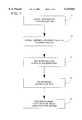
- FIG. 1is a flow diagram illustrating a method of conditioning polishing pads according to a preferred embodiment of the invention.
- FIG. 2is a flow diagram illustrating additional steps to the method of FIG. 1.
- FIG. 3is a top view of a work piece carrier for use with the method of FIG. 1.
- FIG. 4is a top view of another work piece carrier for use with the method of FIG. 1.
- FIG. 5is a graph of exemplary wafer flatness data comparing wafers polished with pads conditioned according to the method of FIG. 1 to wafers polished with pads conditioned by a prior art method.
- FIGS. 1 and 2illustrate a preferred method embodying aspects of the present invention in flow diagram form.
- the present methodadvantageously conditions new polishing pads (not shown) for use with a wafer polishing machine (not shown).
- conventional polishing machinesusually produce highly concave (i.e., dished shape) wafers when installed with new polishing pads.
- the method of the present inventionprovides an economical and quick program for conditioning the pads without numerous, expensive and time-consuming dummy runs.
- the double-side polishing machinepolishes the front and back surfaces of several wafers concurrently to remove damage caused by prior processing operations and to provide a mirror finish.
- the double-side polishing operationusually removes between 24 ⁇ m and 30 ⁇ m (12-15 ⁇ m per side) of thickness from each wafer.
- the machinehas a rotatable lower platen with a polishing surface defined by a polishing pad and is adapted to receive one or more wafer carriers seated on the polishing pad.
- the wafer carriersare rotatable relative to the lower platen and polishing pad and each holds one or more wafers with the front wafer surfaces engaging the polishing pad.
- An upper platensupports a second polishing pad facing opposite the front surfaces of the wafers.
- the upper platenis attached to a motor-driven spindle that rotates the upper platen and second polishing pad relative to the lower platen and wafer carriers.
- the spindlealso provides movement in a vertical direction. By moving the upper platen up and down, the spindle moves the second polishing pad out of and into polishing engagement with the back surfaces of the wafers. This effectively "sandwiches" the wafers between the two polishing pads.
- the force exerted against the wafers by the polishing padsotherwise referred to as the polishing pressure, is generally a function of the downward force exerted by the vertically movable upper platen and polishing pad.
- the machineapplies a polishing slurry containing abrasive particles and a chemical etchant between the polishing pads and the wafers.
- the polishing slurryis a colloidal silica and an alkaline etchant.
- the polishing padswork the slurry against the surfaces of the wafer to concurrently and uniformly remove material from the front and back wafer surfaces. This removes much of the damage caused by lapping and etching operations, substantially improves the flatness of the wafers and produces polished front and back surfaces.
- Machines of this typeusually have several programmable operating parameters such as polishing pressure, upper platen speed, lower platen speed, inner drive ring speed, outer drive ring speed, etchant flow rate, slurry flow rate and the temperature of cooling water used for cooling the platens.
- the lower platenholds a regular polyurethane impregnated polyester felt polishing pad and the upper platen holds an embossed polyurethane impregnated polyester felt polishing pad.
- the embossed pad used on the upper platenhelps retain the wafers on the lower platen after the completion of each cycle run.
- the method of FIG. 1establishes a recipe, or program, for conditioning new polishing pads for use with a double-side or single-side polishing machine.
- An operatorbegins at step 12 by installing new polishing pads on the polishing machine in a conventional manner.
- the operatorthen installs carriers 16 (see FIGS. 3 and 4) on the polishing machine.
- the carriers 16are loaded with work pieces (not shown) rather than with wafers for use in the conditioning, or breaking in, process.
- the work piecesare flat disks of rigid material, such as silicon carbide and/or ceramic, and able to withstand relatively high load forces. Also, the front and back surfaces of the work piece are highly finished to prevent damage to the polishing pads.
- the operatorincreases the load force, or polishing pressure, and the slurry flow rate relative to the normal settings for polishing wafers.
- high polishing pressure in combination with high slurry flow of an alkaline-based silica solutionfor example, rapidly conditions the new pads on both upper and lower platens during a polishing cycle performed at step 24.
- the high pressure and high alkaline-based silica flowact together to highly compress the pads against the work pieces and carriers 16 and load silica from the slurry into their pores.
- Table Ibelow, Table I provides exemplary ranges for the polishing machine's operating parameters, namely polishing pressure and slurry flow rate, according to a preferred embodiment of the invention. Table I also compares the ranges used for conditioning to the conventional ranges for wafer polishing.
- polishing machineat a polishing pressure between about 1000 daN and 3000 daN and with a slurry flow rate between about 120 ml/min and 360 ml/min provides faster compression and silica loading of the polishing pad.
- applying relatively high pressure to the padessentially hardens and flattens it. This improves global flatness characteristics of wafers polished by the pads because the conditioned pads have a more uniform global surface. Also, harder pads are better able to remove long wavelength surface defects than softer pads.
- the double side polishing processcan produce super flat wafers with the conditioned pads immediately after completion of the polishing pad break-in routine of FIG. 1.
- FIG. 2illustrates method steps for providing a check on the pad conditioning routine of FIG. 1 to ensure that the pads will produce wafers having an acceptable flatness.
- the operatorremoves carriers 16 and the work pieces from the polishing machine and, at step 30, replaces them with regular wafer carriers loaded with dummy wafers. Proceeding to steps 32 and 36, the operator decreases the polishing pressure and slurry flow rate to reset the operating parameters for normal wafer polishing.
- a polishing cycle performed on the dummy wafers at step 38produces wafers that can be measured for flatness to ensure that the new polishing pads have been properly conditioned.
- Carriers 16are adapted for use with conventional polishing machines and, thus, have outer dimensional characteristics similar to those of regular wafer carriers. In contrast, however, carriers 16 are particularly well-suited to sustain the high pressure and shearing forces associated with the break-in process that would otherwise likely damage the wafer carriers. As an example, carriers 16 are each about 15 mm to 25 mm thick, generally circular and made from a high performance plastic, such as the materials sold under the trademarks DELRIN®, PEEKTM and TECHRON PPSTM. The thickness of the carriers 16 is slightly less than (by approximately 1000 ⁇ m to 2000 ⁇ m) the thickness of the work pieces.
- carriers 16have one to three openings 40 for holding the work pieces and one to three openings 44 for slurry.
- FIG. 3illustrates carrier 16 suitable for use with the Peter Wolters AC 1400 polishing machine with one work piece opening 40 and three slurry openings 44
- FIG. 4illustrates carrier 16 suitable for use with the Peter Wolters AC 2000 polishing machine with three work piece openings 40 and three slurry openings 44.
- the carrier 16 of FIG. 3is approximately 546 mm in diameter and the work piece opening 40 is approximately 229 mm in diameter and the carrier 16 of FIG. 4 is approximately 724 mm in diameter and the work piece openings 40 are each approximately 229 mm in diameter.
- openings 40, 44are generally circular in shape, carriers 16 are less likely to be damaged under the high load forces of the break-in process than if they were, for example, angular in shape. Further, the slurry openings 44 are sized (e.g., 80 mm in diameter) to accommodate the increased slurry flow rate.
- FIG. 5provides a graph of exemplary flatness data for single crystal silicon wafers polished in accordance with conventional polishing techniques as compared to single crystal silicon wafers polished after conditioning the polishing pads in accordance with the method of FIGS. 1 and 2.
- the graphindicates that pads conditioned according to the present invention produce flatter wafers more quickly (i.e., after fewer runs) than other pads.
- the conditioned padsare better able to eliminate grinding marks than conventional pads. For example, when grinding is used before polishing, Hologenix pictures reveal grinding marks visible on the surfaces of the polished wafers. These marks are visible even after the wafers are polished with pads that have been used on several polishing runs. In contrast, pads conditioned according to the invention remove visible grinding marks as early as the first polishing run following the conditioning routine.
Landscapes
- Engineering & Computer Science (AREA)
- Mechanical Engineering (AREA)
- Physics & Mathematics (AREA)
- Condensed Matter Physics & Semiconductors (AREA)
- General Physics & Mathematics (AREA)
- Manufacturing & Machinery (AREA)
- Computer Hardware Design (AREA)
- Microelectronics & Electronic Packaging (AREA)
- Power Engineering (AREA)
- Finish Polishing, Edge Sharpening, And Grinding By Specific Grinding Devices (AREA)
Abstract
Description
TABLE I ______________________________________ Load Force on Alkaline-based Polishing Pads Silica Flow Rate Cycle Time Name of Program (daN) (ml/min) (min) ______________________________________ Wafer Polishing 200-700 40-120 30-80 Pad Break-In 1000-3000 120-360 10-50 ______________________________________
Claims (20)
Priority Applications (7)
| Application Number | Priority Date | Filing Date | Title |
|---|---|---|---|
| US09/295,127US6135863A (en) | 1999-04-20 | 1999-04-20 | Method of conditioning wafer polishing pads |
| EP00916429AEP1171264A1 (en) | 1999-04-20 | 2000-03-17 | Method of conditioning wafer polishing pads |
| KR1020017013315AKR20020020692A (en) | 1999-04-20 | 2000-03-17 | Method of conditioning wafer polishing pads |
| CN00806470ACN1349446A (en) | 1999-04-20 | 2000-03-17 | Method of conditioning wafer polishing pads |
| JP2000612098AJP2002542613A (en) | 1999-04-20 | 2000-03-17 | How to adjust a wafer polishing pad |
| PCT/US2000/006973WO2000062977A1 (en) | 1999-04-20 | 2000-03-17 | Method of conditioning wafer polishing pads |
| TW089106319ATW466156B (en) | 1999-04-20 | 2000-04-06 | Method of conditioning wafer polishing pads |
Applications Claiming Priority (1)
| Application Number | Priority Date | Filing Date | Title |
|---|---|---|---|
| US09/295,127US6135863A (en) | 1999-04-20 | 1999-04-20 | Method of conditioning wafer polishing pads |
Publications (1)
| Publication Number | Publication Date |
|---|---|
| US6135863Atrue US6135863A (en) | 2000-10-24 |
Family
ID=23136324
Family Applications (1)
| Application Number | Title | Priority Date | Filing Date |
|---|---|---|---|
| US09/295,127Expired - Fee RelatedUS6135863A (en) | 1999-04-20 | 1999-04-20 | Method of conditioning wafer polishing pads |
Country Status (7)
| Country | Link |
|---|---|
| US (1) | US6135863A (en) |
| EP (1) | EP1171264A1 (en) |
| JP (1) | JP2002542613A (en) |
| KR (1) | KR20020020692A (en) |
| CN (1) | CN1349446A (en) |
| TW (1) | TW466156B (en) |
| WO (1) | WO2000062977A1 (en) |
Cited By (12)
| Publication number | Priority date | Publication date | Assignee | Title |
|---|---|---|---|---|
| US20020179244A1 (en)* | 1999-12-27 | 2002-12-05 | Takahiro Hashimoto | Wafer for evaluating machinability of periphery of wafer and method for evaluating machinability of periphery of wafer |
| US20030022596A1 (en)* | 2001-07-27 | 2003-01-30 | Frank Meyer | Method for characterizing the planarizing properties of an expendable material combination in a chemical-mechanical polishing process; simulation technique; and polishing technique |
| DE10162597C1 (en)* | 2001-12-19 | 2003-03-20 | Wacker Siltronic Halbleitermat | Polished semiconductor disc manufacturing method uses polishing between upper and lower polishing plates |
| US20050260924A1 (en)* | 2004-05-21 | 2005-11-24 | Mosel Vitelic, Inc. | Pad break-in method for chemical mechanical polishing tool which polishes with ceria-based slurry |
| US20060140105A1 (en)* | 2002-12-26 | 2006-06-29 | Akihide Minami | Glass substrate for information recording medium and method for producing same |
| US20060270237A1 (en)* | 2003-09-04 | 2006-11-30 | Taiwan Semiconductor Manufacturing Co., Ltd. | Apparatus and method for pre-conditioning CMP polishing pad |
| US20070123154A1 (en)* | 2005-11-28 | 2007-05-31 | Osamu Nabeya | Polishing apparatus |
| US7413986B2 (en) | 2001-06-19 | 2008-08-19 | Applied Materials, Inc. | Feedforward and feedback control for conditioning of chemical mechanical polishing pad |
| US20090181608A1 (en)* | 2008-01-15 | 2009-07-16 | Iv Technologies Co., Ltd. | Polishing pad and fabricating method thereof |
| US20100130111A1 (en)* | 1999-05-17 | 2010-05-27 | Akira Horiguchi | Double side polishing method and apparatus |
| US20100248597A1 (en)* | 2009-03-27 | 2010-09-30 | Kentaro Sakata | Equipment and method for cleaning polishing cloth |
| US11679469B2 (en)* | 2019-08-23 | 2023-06-20 | Taiwan Semiconductor Manufacturing Company, Ltd. | Chemical mechanical planarization tool |
Families Citing this family (3)
| Publication number | Priority date | Publication date | Assignee | Title |
|---|---|---|---|---|
| US7125324B2 (en)* | 2004-03-09 | 2006-10-24 | 3M Innovative Properties Company | Insulated pad conditioner and method of using same |
| CN101279435B (en)* | 2007-04-06 | 2011-03-23 | 中芯国际集成电路制造(上海)有限公司 | Modified type polishing pad regulating apparatus technique |
| CN102339742A (en)* | 2011-09-01 | 2012-02-01 | 上海宏力半导体制造有限公司 | Method for pre-polishing polishing pad by adopting polysilicon CMP (Chemical Mechanical Polishing) process |
Citations (12)
| Publication number | Priority date | Publication date | Assignee | Title |
|---|---|---|---|---|
| US5245790A (en)* | 1992-02-14 | 1993-09-21 | Lsi Logic Corporation | Ultrasonic energy enhanced chemi-mechanical polishing of silicon wafers |
| US5329734A (en)* | 1993-04-30 | 1994-07-19 | Motorola, Inc. | Polishing pads used to chemical-mechanical polish a semiconductor substrate |
| US5422316A (en)* | 1994-03-18 | 1995-06-06 | Memc Electronic Materials, Inc. | Semiconductor wafer polisher and method |
| US5527424A (en)* | 1995-01-30 | 1996-06-18 | Motorola, Inc. | Preconditioner for a polishing pad and method for using the same |
| US5672095A (en)* | 1995-09-29 | 1997-09-30 | Intel Corporation | Elimination of pad conditioning in a chemical mechanical polishing process |
| US5746771A (en)* | 1996-09-30 | 1998-05-05 | Wright Medical Technology, Inc. | Calcar collar instrumentation |
| US5797789A (en)* | 1996-03-28 | 1998-08-25 | Shin-Etsu Handotai Co., Ltd. | Polishing system |
| US5827395A (en)* | 1994-06-03 | 1998-10-27 | Shin-Etsu Handotai Co., Ltd. | Polishing pad used for polishing silicon wafers and polishing method using the same |
| US5840202A (en)* | 1996-04-26 | 1998-11-24 | Memc Electronic Materials, Inc. | Apparatus and method for shaping polishing pads |
| US5890951A (en)* | 1996-04-15 | 1999-04-06 | Lsi Logic Corporation | Utility wafer for chemical-mechanical planarization |
| US5944590A (en)* | 1995-11-14 | 1999-08-31 | Nec Corporation | Polishing apparatus having retainer ring rounded along outer periphery of lower surface and method of regulating retainer ring to appropriate configuration |
| US6007411A (en)* | 1997-06-19 | 1999-12-28 | Interantional Business Machines Corporation | Wafer carrier for chemical mechanical polishing |
Family Cites Families (3)
| Publication number | Priority date | Publication date | Assignee | Title |
|---|---|---|---|---|
| TW367551B (en)* | 1993-06-17 | 1999-08-21 | Freescale Semiconductor Inc | Polishing pad and a process for polishing |
| JP3778594B2 (en)* | 1995-07-18 | 2006-05-24 | 株式会社荏原製作所 | Dressing method |
| TW344695B (en)* | 1995-08-24 | 1998-11-11 | Matsushita Electric Industrial Co Ltd | Method for polishing semiconductor substrate |
- 1999
- 1999-04-20USUS09/295,127patent/US6135863A/ennot_activeExpired - Fee Related
- 2000
- 2000-03-17EPEP00916429Apatent/EP1171264A1/ennot_activeWithdrawn
- 2000-03-17KRKR1020017013315Apatent/KR20020020692A/ennot_activeWithdrawn
- 2000-03-17CNCN00806470Apatent/CN1349446A/enactivePending
- 2000-03-17JPJP2000612098Apatent/JP2002542613A/ennot_activeWithdrawn
- 2000-03-17WOPCT/US2000/006973patent/WO2000062977A1/ennot_activeApplication Discontinuation
- 2000-04-06TWTW089106319Apatent/TW466156B/ennot_activeIP Right Cessation
Patent Citations (12)
| Publication number | Priority date | Publication date | Assignee | Title |
|---|---|---|---|---|
| US5245790A (en)* | 1992-02-14 | 1993-09-21 | Lsi Logic Corporation | Ultrasonic energy enhanced chemi-mechanical polishing of silicon wafers |
| US5329734A (en)* | 1993-04-30 | 1994-07-19 | Motorola, Inc. | Polishing pads used to chemical-mechanical polish a semiconductor substrate |
| US5422316A (en)* | 1994-03-18 | 1995-06-06 | Memc Electronic Materials, Inc. | Semiconductor wafer polisher and method |
| US5827395A (en)* | 1994-06-03 | 1998-10-27 | Shin-Etsu Handotai Co., Ltd. | Polishing pad used for polishing silicon wafers and polishing method using the same |
| US5527424A (en)* | 1995-01-30 | 1996-06-18 | Motorola, Inc. | Preconditioner for a polishing pad and method for using the same |
| US5672095A (en)* | 1995-09-29 | 1997-09-30 | Intel Corporation | Elimination of pad conditioning in a chemical mechanical polishing process |
| US5944590A (en)* | 1995-11-14 | 1999-08-31 | Nec Corporation | Polishing apparatus having retainer ring rounded along outer periphery of lower surface and method of regulating retainer ring to appropriate configuration |
| US5797789A (en)* | 1996-03-28 | 1998-08-25 | Shin-Etsu Handotai Co., Ltd. | Polishing system |
| US5890951A (en)* | 1996-04-15 | 1999-04-06 | Lsi Logic Corporation | Utility wafer for chemical-mechanical planarization |
| US5840202A (en)* | 1996-04-26 | 1998-11-24 | Memc Electronic Materials, Inc. | Apparatus and method for shaping polishing pads |
| US5746771A (en)* | 1996-09-30 | 1998-05-05 | Wright Medical Technology, Inc. | Calcar collar instrumentation |
| US6007411A (en)* | 1997-06-19 | 1999-12-28 | Interantional Business Machines Corporation | Wafer carrier for chemical mechanical polishing |
Cited By (21)
| Publication number | Priority date | Publication date | Assignee | Title |
|---|---|---|---|---|
| US8002610B2 (en)* | 1999-05-17 | 2011-08-23 | Sumitomo Mitsubishi Silicon Corporation | Double side polishing method and apparatus |
| US20100130111A1 (en)* | 1999-05-17 | 2010-05-27 | Akira Horiguchi | Double side polishing method and apparatus |
| US20020179244A1 (en)* | 1999-12-27 | 2002-12-05 | Takahiro Hashimoto | Wafer for evaluating machinability of periphery of wafer and method for evaluating machinability of periphery of wafer |
| US6722954B2 (en)* | 1999-12-27 | 2004-04-20 | Shin-Etsu Handotai Co., Ltd. | Wafer for evaluating machinability of periphery of wafer and method for evaluating machinability of periphery of wafer |
| US7413986B2 (en) | 2001-06-19 | 2008-08-19 | Applied Materials, Inc. | Feedforward and feedback control for conditioning of chemical mechanical polishing pad |
| US6682398B2 (en)* | 2001-07-27 | 2004-01-27 | Infineon Technologies Ag | Method for characterizing the planarizing properties of an expendable material combination in a chemical-mechanical polishing process; simulation technique; and polishing technique |
| US20030022596A1 (en)* | 2001-07-27 | 2003-01-30 | Frank Meyer | Method for characterizing the planarizing properties of an expendable material combination in a chemical-mechanical polishing process; simulation technique; and polishing technique |
| DE10162597C1 (en)* | 2001-12-19 | 2003-03-20 | Wacker Siltronic Halbleitermat | Polished semiconductor disc manufacturing method uses polishing between upper and lower polishing plates |
| US20060140105A1 (en)* | 2002-12-26 | 2006-06-29 | Akihide Minami | Glass substrate for information recording medium and method for producing same |
| US20080220700A1 (en)* | 2002-12-26 | 2008-09-11 | Hoya Corporation | Glass Substrate for Information Recording Medium and Method for Producing the Same |
| US7500904B2 (en) | 2002-12-26 | 2009-03-10 | Hoya Corporation | Glass substrate for information recording medium and method for producing same |
| US8021566B2 (en)* | 2003-09-04 | 2011-09-20 | Taiwan Semiconductor Manufacturing Co., Ltd. | Method for pre-conditioning CMP polishing pad |
| US20060270237A1 (en)* | 2003-09-04 | 2006-11-30 | Taiwan Semiconductor Manufacturing Co., Ltd. | Apparatus and method for pre-conditioning CMP polishing pad |
| US20050260924A1 (en)* | 2004-05-21 | 2005-11-24 | Mosel Vitelic, Inc. | Pad break-in method for chemical mechanical polishing tool which polishes with ceria-based slurry |
| US7070484B2 (en)* | 2004-05-21 | 2006-07-04 | Mosel Vitelic, Inc. | Pad break-in method for chemical mechanical polishing tool which polishes with ceria-based slurry |
| US20070123154A1 (en)* | 2005-11-28 | 2007-05-31 | Osamu Nabeya | Polishing apparatus |
| US20090181608A1 (en)* | 2008-01-15 | 2009-07-16 | Iv Technologies Co., Ltd. | Polishing pad and fabricating method thereof |
| US8517800B2 (en)* | 2008-01-15 | 2013-08-27 | Iv Technologies Co., Ltd. | Polishing pad and fabricating method thereof |
| US20100248597A1 (en)* | 2009-03-27 | 2010-09-30 | Kentaro Sakata | Equipment and method for cleaning polishing cloth |
| US11679469B2 (en)* | 2019-08-23 | 2023-06-20 | Taiwan Semiconductor Manufacturing Company, Ltd. | Chemical mechanical planarization tool |
| US12172263B2 (en) | 2019-08-23 | 2024-12-24 | Taiwan Semiconductor Manufacturing Company, Ltd. | Chemical mechanical planarization tool |
Also Published As
| Publication number | Publication date |
|---|---|
| EP1171264A1 (en) | 2002-01-16 |
| CN1349446A (en) | 2002-05-15 |
| JP2002542613A (en) | 2002-12-10 |
| TW466156B (en) | 2001-12-01 |
| WO2000062977A1 (en) | 2000-10-26 |
| WO2000062977A9 (en) | 2001-12-27 |
| KR20020020692A (en) | 2002-03-15 |
Similar Documents
| Publication | Publication Date | Title |
|---|---|---|
| US6135863A (en) | Method of conditioning wafer polishing pads | |
| JP3846706B2 (en) | Polishing method and polishing apparatus for wafer outer peripheral chamfer | |
| EP1501119B1 (en) | Semiconductor wafer manufacturing method and wafer | |
| JP5995825B2 (en) | Method for polishing at least one wafer | |
| US6325709B1 (en) | Rounded surface for the pad conditioner using high temperature brazing | |
| US6093087A (en) | Wafer processing machine and a processing method thereby | |
| KR100737879B1 (en) | Method of manufacturing a semiconductor wafer | |
| US4054010A (en) | Apparatus for grinding edges of planar workpieces | |
| WO2010013390A1 (en) | Wafer polishing method and double side polishing apparatus | |
| US7416962B2 (en) | Method for processing a semiconductor wafer including back side grinding | |
| JPH09270401A (en) | Polishing method of semiconductor wafer | |
| JP2002512894A (en) | Chemical mechanical polishing using multiple polishing pads | |
| KR20010092732A (en) | Method of processing semiconductor wafers to build in back surface damage | |
| KR20010030567A (en) | Method of processing semiconductor wafers | |
| US7695347B2 (en) | Method and pad for polishing wafer | |
| US5840202A (en) | Apparatus and method for shaping polishing pads | |
| US20040038544A1 (en) | Method for processing a semiconductor wafer using double-side polishing | |
| GB2058620A (en) | A method and apparatus for effecting the lapping of wafers of semiconductive material | |
| JP2001156030A (en) | Grinding roller for semiconductor wafer and method for grinding semiconductor wafer using the same | |
| US6857942B1 (en) | Apparatus and method for pre-conditioning a conditioning disc | |
| WO2000047369A1 (en) | Method of polishing semiconductor wafers | |
| KR20010040249A (en) | Polishing apparatus and method for producing semiconductors using the apparatus | |
| JP3821944B2 (en) | Wafer single wafer polishing method and apparatus | |
| JP4122800B2 (en) | Semiconductor wafer polishing method | |
| JPH1126405A (en) | Polishing equipment |
Legal Events
| Date | Code | Title | Description |
|---|---|---|---|
| AS | Assignment | Owner name:MEMC ELECTRONIC MATERIALS, INC., MISSOURI Free format text:ASSIGNMENT OF ASSIGNORS INTEREST;ASSIGNORS:ZHANG, DAVID;VOGELGESANG, RALPH V.;ERK, HENRY F.;REEL/FRAME:009916/0284;SIGNING DATES FROM 19990409 TO 19990415 | |
| AS | Assignment | Owner name:MEMC ELECTRONIC MATERIALS, INC., MISSOURI Free format text:TERMINATION OF SECURITY INTEREST;ASSIGNOR:E.ON AG;REEL/FRAME:012263/0944 Effective date:20011113 Owner name:CITICORP USA, INC., DELAWARE Free format text:SECURITY INTEREST;ASSIGNORS:MEMC PASADENA, INC.;PLASMASIL, L.L.C.;SIBOND, L.L.C.;AND OTHERS;REEL/FRAME:012273/0145 Effective date:20011113 Owner name:CITICORP USA, INC., DELAWARE Free format text:SECURITY AGREEMENT;ASSIGNORS:MEMC PASADENA, INC.;PLASMASIL, L.L.C.;SIBOND, L.L.C.;AND OTHERS;REEL/FRAME:012280/0161 Effective date:20011113 | |
| AS | Assignment | Owner name:E. ON AG, GERMANY Free format text:SECURITY INTEREST;ASSIGNOR:MEMC ELECTRONIC MATERIALS, INC.;REEL/FRAME:012407/0806 Effective date:20011025 | |
| AS | Assignment | Owner name:CITICORP USA, INC., DELAWARE Free format text:SECURITY AGREEMENT;ASSIGNORS:MEMC PASADENA, INC.;PLASMASIL, L.L.C.;SIBOND, L.L.C.;AND OTHERS;REEL/FRAME:012365/0345 Effective date:20011221 | |
| AS | Assignment | Owner name:CITICORP USA, INC., DELAWARE Free format text:SECURITY AGREEMENT;ASSIGNORS:MEMC ELECTRONIC MATERIALS, INC.;MEMC PASADENA, INC.;PLASMASIL, L.L.C.;AND OTHERS;REEL/FRAME:013964/0378;SIGNING DATES FROM 20020303 TO 20030303 Owner name:CITICORP USA, INC., DELAWARE Free format text:SECURITY AGREEMENT;ASSIGNORS:MEMC ELECTRONIC MATERIALS, INC.;MEMC PASADENA, INC.;PLASMASIL, L.L.C.;AND OTHERS;SIGNING DATES FROM 20020303 TO 20030303;REEL/FRAME:013964/0378 | |
| REMI | Maintenance fee reminder mailed | ||
| LAPS | Lapse for failure to pay maintenance fees | ||
| STCH | Information on status: patent discontinuation | Free format text:PATENT EXPIRED DUE TO NONPAYMENT OF MAINTENANCE FEES UNDER 37 CFR 1.362 | |
| FP | Lapsed due to failure to pay maintenance fee | Effective date:20041024 | |
| AS | Assignment | Owner name:MEMC ELECTRONIC MATERIALS, INC., MISSOURI Free format text:RELEASE OF SECURITY INTEREST;ASSIGNOR:CITICORP USA, INC.;REEL/FRAME:016641/0045 Effective date:20050602 | |
| AS | Assignment | Owner name:MEMC SOUTHWEST INC., MISSOURI Free format text:RELEASE OF SECURITY INTEREST TO REEL/FRAME: 012280/0161;ASSIGNOR:CITICORP USA, INC.;REEL/FRAME:032458/0794 Effective date:20140313 Owner name:MEMC ELECTRONIC MATERIALS, INC. (NOW KNOWN AS SUNE Free format text:RELEASE OF SECURITY INTEREST TO REEL/FRAME: 012280/0161;ASSIGNOR:CITICORP USA, INC.;REEL/FRAME:032458/0794 Effective date:20140313 Owner name:MEMC INTERNATIONAL, INC. (NOW KNOWN AS SUNEDISON I Free format text:RELEASE OF SECURITY INTEREST TO REEL/FRAME: 012280/0161;ASSIGNOR:CITICORP USA, INC.;REEL/FRAME:032458/0794 Effective date:20140313 Owner name:MEMC PASADENA, INC., TEXAS Free format text:RELEASE OF SECURITY INTEREST TO REEL/FRAME: 012280/0161;ASSIGNOR:CITICORP USA, INC.;REEL/FRAME:032458/0794 Effective date:20140313 Owner name:SIBOND, L.L.C., MISSOURI Free format text:RELEASE OF SECURITY INTEREST TO REEL/FRAME: 012280/0161;ASSIGNOR:CITICORP USA, INC.;REEL/FRAME:032458/0794 Effective date:20140313 Owner name:PLASMASIL, L.L.C., MISSOURI Free format text:RELEASE OF SECURITY INTEREST TO REEL/FRAME: 012280/0161;ASSIGNOR:CITICORP USA, INC.;REEL/FRAME:032458/0794 Effective date:20140313 |