US6134703A - Process for programming PLDs and embedded non-volatile memories - Google Patents
Process for programming PLDs and embedded non-volatile memoriesDownload PDFInfo
- Publication number
- US6134703A US6134703AUS08/996,530US99653097AUS6134703AUS 6134703 AUS6134703 AUS 6134703AUS 99653097 AUS99653097 AUS 99653097AUS 6134703 AUS6134703 AUS 6134703A
- Authority
- US
- United States
- Prior art keywords
- row
- pattern
- matrix
- patterns
- programming
- Prior art date
- Legal status (The legal status is an assumption and is not a legal conclusion. Google has not performed a legal analysis and makes no representation as to the accuracy of the status listed.)
- Expired - Lifetime
Links
Images


Classifications
- G—PHYSICS
- G06—COMPUTING OR CALCULATING; COUNTING
- G06F—ELECTRIC DIGITAL DATA PROCESSING
- G06F30/00—Computer-aided design [CAD]
- G06F30/30—Circuit design
- G06F30/34—Circuit design for reconfigurable circuits, e.g. field programmable gate arrays [FPGA] or programmable logic devices [PLD]
Definitions
- Appendix Awhich is a part of the present disclosure, is attached herewith in a microfiche consisting of a total of 1 sheet that contains a total of 58 frames.
- Appendix Ais a listing of a computer program, which computes a minimal basis set of the "pattern matrix", which is a matrix containing rows of bit patterns (hereinafter "row patterns") used for programming a programmable logic device.
- the computer programwritten in the C programming language, can be compiled by most C language compilers, for example, by a C compiler running on the Solaris 1.X operating system available from Sun Microsystems of Sunnyvale, Calif.
- the present inventionrelates to non-volatile computer memories, and, in particular, to programming of programmable logic devices (PLDs).
- PLDsprogrammable logic devices
- ROMread-only memory
- PROMprogrammable ROM
- PLDprogrammable logic (array) devices
- EPROMerasable PROM
- EPLDserasable PLDs
- FIG. 1illustrates a basic structure of an EPROM 100 with a matrix of 2 n rows and 4 columns (i.e., 2 n ⁇ 4 bit-cells or 2 n 4-bit words are programmable).
- an EPROMreceives an address (for both programming the EPROM and retrieving a word from it) in parallel, and provides a parallel data output.
- a row address decoder 101accepts an n-bit address 110 as input and activates one of its 2 n output lines 120 connected to respective 2 n rows of the EPROM.
- one of the corresponding row among the 2 n rows of the EPROMis addressed.
- 4 bit-cells of an activated rowe.g., the first row 120-1, is programmed in parallel (i.e., simultaneously).
- FIG. 2illustrates a basic structure of an EPLD 200.
- EPLDsCompared to EPROMs, the number of bits that can be programmed simultaneously is much larger. This is because EPLDs' usage is mainly for reading out Boolean function values rather than reading or programming the device memory's contents, therefore allowing programming (which rarely happens) be performed on more bits simultaneously.
- one row of EPLD 200is activated, for example, using a row address shift register 201.
- an EPLD of the same sizei.e., 2 n ⁇ 4 bit-cells
- row address shift register 201contains a bit pattern consisting of one ⁇ 1 ⁇ bit and (2 n -1) ⁇ 0 ⁇ bits, where the position of the single ⁇ 1 ⁇ bit designates which row is to be activated for programming. For example, a ⁇ 1 ⁇ bit at the j-th position of row address shift register 201 activates the j-th line 220-j, which in turn activates the j-th row of the EPLD matrix.
- the rows of EPLD 200are sequentially accessed by clocking the shift register 201. When a certain row is activated, the programming data is loaded serially via four 1-bit data shift registers 202, 203, 204 and 205 for that particular row alone. This limitation results in serial programming of data. As a consequence, for such EPLDs, programming becomes time-consuming.
- EPROM 100 and EPLD 200each has only 4 columns to facilitate explanation. In practice, the number of columns of an EPROM or an EPLD is far greater than 4, e.g., 128 columns. Also, the structures respectively related to output of programmed words from EPROM 100 and EPLD 200 are omitted from FIGS. 1 and 2. One skilled in the art would understand how to output data from EPROMs and EPLDs.
- Time required for programminglimits the number of EPLDs that can be tested.
- An EPLDis typically programmed with ten, twenty or even more programming patterns during a test (i.e., many more than an EPROM would require).
- the time required to program the devicemay constitute almost all the time actually spent on the test. Therefore, a faster method of programming an EPLD can be of great savings.
- Another scheme heretofore employedinvolves the "walking" a ⁇ 1 ⁇ bit through the four data shift registers 202-205 of FIG. 2, serially activating the corresponding columns 206-209, respectively, while different sets of row addresses are enabled. In general, this method is more efficient than the traditional method only when there are much more rows than there are columns.
- a method for reducing the time to program an EPLD using a basis set of the desired rows of programming patternis described.
- a basis setis a set of row patterns from which all of the row patterns can be derived using one or more Boolean operations.
- a minimal basis set of a given pattern matrixis a basis set with the smallest number of members (i.e., row patterns).
- a row of an EPLDis programmed by loading a row pattern.
- row patterns of a basis setare loaded one row pattern at a time into as many rows of the EPLD as possible simultaneously.
- the multiple programminghas the effect of programming the row of the EPLD with a result of applying a Boolean OR operation on the multiple row patterns. Since the number of row patterns in a basis set is, in most cases, less than the number of rows of the pattern matrix, the overall process takes significantly less time than programming the rows using most prior art methods. The time saving is particularly significant when a minimal basis set is used.
- FIG. 1illustrates a representative EPROM design 100 with a 1-out-of-2 n row address decoder 101, four 1-bit data registers 102-105 and EPROM matrix columns 106-109.
- FIG. 2illustrates a representative EPLD design 200 differing from an EPROM design due to constraint on the number of pins.
- the illustrated EPLD 200has a row address shift register 201, four 1-bit data shift registers 202-205, and EPLD matrix columns 206-209.
- FIG. 3illustrates steps 310-360 for finding a minimal basis set of a given pattern matrix.
- FIG. 4illustrates substeps 320A-320C for carrying out step 320 of performing XNOR operations, which is one of the steps shown in FIG. 3.
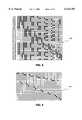
- FIG. 5illustrates a 32 ⁇ 32 pattern matrix 500.
- FIG. 6illustrates a 20 ⁇ 32 basis set matrix 600 of the pattern matrix shown in FIG. 5.
- EPLDsThere are two types of EPLDs: in one type, an unprogrammed cell is defaulted to logic ⁇ 0 ⁇ and programming sets the bit to ⁇ 1 ⁇ , if appropriate. In the other type, an unprogrammed bit is defaulted to logic ⁇ 1 ⁇ and programming sets the bit to ⁇ 0 ⁇ , if appropriate. In the first type, if a row of an EPLD is programmed multiple times with different row patterns, the result is a row pattern which is the logical "sum” (i.e., logical "ORing") of the different row patterns. In EPLDs where programming is accomplished by setting ⁇ 1 ⁇ bits to ⁇ 0 ⁇ bits, all the programmable bits are initialized to ⁇ 1 ⁇ before programming. Here, if a row of an EPLD is programmed multiple times with multiple row patterns, the result is a row pattern which is the logical "product" (i.e., bit-wise logical "ANDing") of the row patterns.
- logical "product"i.e., bit-wise logical "
- the present inventionis illustrated using examples of EPLDs in which programming is accomplished by setting selected ⁇ 0 ⁇ bits to ⁇ 1 ⁇ bits.
- One skilled in the artwill appreciate that the present invention can be applied to EPLDs where programming is achieved by setting ⁇ 1 ⁇ bits to ⁇ 0 ⁇ bits using analogous procedures.
- row pattern Cis the logical sum (i.e., ORing) of row patterns A and B.
- row 3can be programmed in two steps, by first loading row pattern A simultaneously into rows 1 and 3, and then loading row pattern B simultaneously into rows 2 and 3.
- loading twicesuffices. Therefore significant programming time can be saved by utilizing the fact that some row patterns can be expressed as logical sums of other row patterns.
- the described methodcan be further improved by using row patterns that need not be found in any row of the pattern matrix.
- row pattern Dcan be derived as the logical sum of row patterns A, F, L, P and R.
- any of the row patterns A-Tcan now be generated from a smaller set of row patterns: B, F, H, J, L, N, P, R, T and U.
- a total of ten primitive row patternswill suffice to do all programming, which is less than the previous 12 primitive row patterns.
- the row patterns to be loaded into the EPLDcan be decomposed into a set of primitive row patterns (each of which need not occur in the pattern matrix).
- Each of these primitive row patternsis referred to as a "basis" by analogy with the theory of vector spaces. More than one basis set that derives a given pattern matrix may exist, some basis sets having less members than others. Although a substantial savings can be realized even with a non-minimal basis set, programming with a minimal basis set (i.e., a basis set with the smallest number of rows) results in the least programming time.
- a minimal basis setcan be found either exhaustively, or by the method described below.
- FIG. 3illustrates steps 310-360 (which roughly correspond to steps 1-4 below) for finding a minimal basis set, given an m ⁇ n pattern matrix, i.e., m row patterns with n bits each:
- Step 1Create an empty set named BASIS SET.
- Step 2Perform an XNOR operation on every possible pair of n columns of the pattern matrix.
- Step 3Select the most frequently occurring m-bit XNOR result, line up the XNOR result with the pattern matrix as if the m-bit result is the (n+1)-th column of the pattern matrix, and use the bit pattern of the result to derive two subsets of row patterns as follows:
- Step 4For each subset, if all rows in a subset of row patterns are primitive, the subset is "irreducible”; otherwise the subset is "reducible”. Each row patterns in the irreducible subset is added to the BASIS SET unless the row pattern is already in the BASIS SET. If the subset is reducible, Steps 2-4 are performed on the subset.
- steps 2.1-2.3are respectively illustrated in FIG. 4 as steps 320A-320C.
- the following stepsillustrate a detailed example of the present invention, which further includes additional steps that make the overall process of finding a minimal basis set quicker for a given pattern matrix.
- Step 3.1Create an empty set named BASIS SET.
- Step 3.2Label each row of the pattern matrix with a membership set, whose single element is the identification (ID) number of the row, e.g., the first row of the pattern matrix is labeled as ⁇ 0 ⁇ .
- IDthe identification number of the row
- Step 3.3Delete the rows in the pattern matrix consisting only of ⁇ 0 ⁇ bits (i.e., rows that do not need any programming) and call the resulting matrix Z.
- Step 3.4Create a matrix R by eliminating duplicate rows from matrix Z, and then label each remaining unique row pattern of matrix R with an updated membership set consisting of the ID numbers of identical row patterns. For example, if there were rows 1, 2 and 4 with pattern 11110101 in matrix Z, delete two redundant rows (e.g., rows 2 and 4) of matrix Z and tag the remaining row pattern in matrix R with membership set ⁇ 1, 2, 4 ⁇ .
- Step 3.5From matrix R, move each row pattern ("single-l-bit row") with a single ⁇ 1 ⁇ bit (e.g., 00010000), which is clearly primitive, to set BASIS SET if the row pattern is not already a member of BASIS SET.
- ⁇ 1 ⁇ bite.g. 00010000
- Step 3.6For each single-1-bit row, in all other rows of matrix R, set to ⁇ 0 ⁇ the bit corresponding to the ⁇ 1 ⁇ bit of the single-bit row. For example, if a single-1-bit row had pattern 00001000, then change a row pattern 11111110 of matrix R to 11110110.
- Step 3.7Repeat steps 3.4-3.6 until no duplicate rows and single-bit rows exist. Call the resulting matrix D.
- Step 3.8Delete all columns without any 1 bit (step 3.8.1), tag each column of matrix D with the column's bit position (step 3.8.2), eliminate duplicate columns from matrix D (step 3.8.3), and express the bit positions of the eliminated duplicate columns together with remaining unique column's bit position (step 3.8.4). Call the resulting matrix D'.
- Step 3.9Perform an XNOR operation between every pair of columns of matrix D'. XNOR operation of two bits results in 1 when two bits are the same and 0 when two bits differ.
- the 4 columns in matrix D'will produce 6 XNOR results from 6 possible pairings of rows. For example, the first two columns (transposed into rows below for convenience) are XNORed as follows:
- Step 3.10Order the XNOR results in decreasing order of frequency, i.e., with the most frequently occurring pattern being the first and the least frequently occurring pattern the last. (Not all XNOR results will be unique, occurring repeatedly. For example, if pattern A occurred 7 times, pattern B occurred 4 times and pattern C 3 times, the three patterns will be ordered as A B C.)
- Step 3.1 1Delete any XNOR pattern whose number of occurrences is less than the number of 1's in the pattern. For example, if pattern 11010001 as an XNOR result occurred 3 times (less than 4, which is the number of 1's in the pattern), this pattern is discarded.
- Step 3.12Each resulting XNOR pattern suggests a way to split row patterns of matrix D to form two matrices D1 and D2 such that row patterns corresponding to 1's in an XNOR pattern belong to D1 and row patterns corresponding to 0's belong to D0.
- XNOR pattern 01111110suggests that the first row pattern and the eighth row pattern should be put in matrix D0, and the rest of the row patterns in matrix D1.
- One heuristic rulechooses the most frequently occurring XNOR pattern for splitting matrix D.
- Step 3.13For each of matrices D0 and D1, one of three possible situations can arise:
- FIG. 5shows a 32 ⁇ 32 pattern matrix 500 for programming a portion of an EPLD.
- Each cell with a "dot" in pattern matrix 500represents an EPLD bit-cell to be programmed to ⁇ 1 ⁇ and each one without a "dot” represents a cell to be programmed to ⁇ 0 ⁇ . Since no two row patterns in pattern 500 are identical, no time savings can be realized by the prior art method of programming identical rows simultaneously. Also, the prior art method of serially programming each column of pattern matrix 500 will require 32 programming operations, i.e., no savings, since the matrix does not have fewer columns than it has rows . Finally, since no row can be derived from other two or more rows, it will not be possible to express any row as the sum of other rows. However, with the choice of 20 basis row patterns 600 shown in FIG. 6, the number of programming operations becomes 20 (instead of 32).
Landscapes
- Engineering & Computer Science (AREA)
- Computer Hardware Design (AREA)
- Physics & Mathematics (AREA)
- Theoretical Computer Science (AREA)
- Evolutionary Computation (AREA)
- Geometry (AREA)
- General Engineering & Computer Science (AREA)
- General Physics & Mathematics (AREA)
- Read Only Memory (AREA)
- Logic Circuits (AREA)
- Programmable Controllers (AREA)
Abstract
Description
______________________________________ A: 000000010000001000001000000100101000001000010000 B: 010010100010010001000010000010000001000010000010 C: 010010110010011001001010000110101001001010010010 ______________________________________
______________________________________ A: 10010110011001011001100101100110010110011001011001 B: 00000001000000000100000000010000000001000000000100 C: 01111001110111100111011110011101111001110111100111 D: 11111110111111111011111111101111111110111111111011 E: 11111111011111111101111111110111111111011111111101 F: 00000000100000000010000000001000000000100000000010 G: 11111101111111110111111111011111111101111111110111 H: 00000010000000001000000000100000000010000000001000 I: 11111011111111101111111110111111111011111111101111 J: 00000100000000010000000001000000000100000000010000 K: 11110111111111011111111101111111110111111111011111 L: 00001000000000100000000010000000001000000000100000 M: 11101111111110111111111011111111101111111110111111 N: 00010000000001000000000100000000010000000001000000 O: 11011111111101111111110111111111011111111101111111 P: 00100000000010000000001000000000100000000010000000 Q: 10111111111011111111101111111110111111111011111111 R: 01000000000100000000010000000001000000000100000000 S: 01111111110111111111011111111101111111110111111111 T: 10000000001000000000100000000010000000001000000000 ______________________________________
______________________________________ U: 00000000010000000001000000000100000000010000000001 ______________________________________
______________________________________ bit 0bit 1bit 2/5bit 3 ______________________________________ 1 1 1 1 0 1 1 0 0 1 1 0 0 1 1 1 1 0 1 1 0 1 1 0 0 1 1 1 0 0 1 0. ______________________________________
______________________________________ 10001000 11110110 10000001 ______________________________________
Claims (7)
Priority Applications (2)
| Application Number | Priority Date | Filing Date | Title |
|---|---|---|---|
| US08/996,530US6134703A (en) | 1997-12-23 | 1997-12-23 | Process for programming PLDs and embedded non-volatile memories |
| EP98310617AEP0926609A3 (en) | 1997-12-23 | 1998-12-22 | Process for programming PLDs and embedded non-volatile memories |
Applications Claiming Priority (1)
| Application Number | Priority Date | Filing Date | Title |
|---|---|---|---|
| US08/996,530US6134703A (en) | 1997-12-23 | 1997-12-23 | Process for programming PLDs and embedded non-volatile memories |
Publications (1)
| Publication Number | Publication Date |
|---|---|
| US6134703Atrue US6134703A (en) | 2000-10-17 |
Family
ID=25543012
Family Applications (1)
| Application Number | Title | Priority Date | Filing Date |
|---|---|---|---|
| US08/996,530Expired - LifetimeUS6134703A (en) | 1997-12-23 | 1997-12-23 | Process for programming PLDs and embedded non-volatile memories |
Country Status (2)
| Country | Link |
|---|---|
| US (1) | US6134703A (en) |
| EP (1) | EP0926609A3 (en) |
Cited By (2)
| Publication number | Priority date | Publication date | Assignee | Title |
|---|---|---|---|---|
| US6538468B1 (en) | 2000-07-31 | 2003-03-25 | Cypress Semiconductor Corporation | Method and apparatus for multiple boot-up functionalities for a programmable logic device (PLD) |
| WO2008023152A1 (en)* | 2006-08-25 | 2008-02-28 | Imperial Innovations Limited | Logic circuit |
Citations (12)
| Publication number | Priority date | Publication date | Assignee | Title |
|---|---|---|---|---|
| US4488246A (en)* | 1980-11-03 | 1984-12-11 | Societe pour l'Etude et la Fabrication des Circuits Integres Speciaux | Integrated logic network with simplified programming |
| US5256918A (en)* | 1991-02-27 | 1993-10-26 | Kabushiki Kaisha Toshiba | Programmable logic circuit |
| US5329179A (en)* | 1992-10-05 | 1994-07-12 | Lattice Semiconductor Corporation | Arrangement for parallel programming of in-system programmable IC logical devices |
| US5394031A (en)* | 1993-12-08 | 1995-02-28 | At&T Corp. | Apparatus and method to improve programming speed of field programmable gate arrays |
| US5521835A (en)* | 1992-03-27 | 1996-05-28 | Xilinx, Inc. | Method for programming an FPLD using a library-based technology mapping algorithm |
| US5526276A (en)* | 1994-04-21 | 1996-06-11 | Quicklogic Corporation | Select set-based technology mapping method and apparatus |
| US5543730A (en)* | 1995-05-17 | 1996-08-06 | Altera Corporation | Techniques for programming programmable logic array devices |
| US5635855A (en)* | 1995-07-21 | 1997-06-03 | Lattice Semiconductor Corporation | Method for simultaneous programming of in-system programmable integrated circuits |
| US5684980A (en)* | 1992-07-29 | 1997-11-04 | Virtual Computer Corporation | FPGA virtual computer for executing a sequence of program instructions by successively reconfiguring a group of FPGA in response to those instructions |
| US5861761A (en)* | 1992-11-05 | 1999-01-19 | Xilinx, Inc. | Hierarchically connectable configurable cellular array |
| US6023755A (en)* | 1992-07-29 | 2000-02-08 | Virtual Computer Corporation | Computer with programmable arrays which are reconfigurable in response to instructions to be executed |
| US6023566A (en)* | 1997-04-14 | 2000-02-08 | Cadence Design Systems | Cluster matching for circuit implementation |
Family Cites Families (1)
| Publication number | Priority date | Publication date | Assignee | Title |
|---|---|---|---|---|
| US5159599A (en)* | 1990-07-31 | 1992-10-27 | Sgs-Thomson Microelectronics, Inc. | High speed testing for programmable logic devices |
- 1997
- 1997-12-23USUS08/996,530patent/US6134703A/ennot_activeExpired - Lifetime
- 1998
- 1998-12-22EPEP98310617Apatent/EP0926609A3/ennot_activeWithdrawn
Patent Citations (12)
| Publication number | Priority date | Publication date | Assignee | Title |
|---|---|---|---|---|
| US4488246A (en)* | 1980-11-03 | 1984-12-11 | Societe pour l'Etude et la Fabrication des Circuits Integres Speciaux | Integrated logic network with simplified programming |
| US5256918A (en)* | 1991-02-27 | 1993-10-26 | Kabushiki Kaisha Toshiba | Programmable logic circuit |
| US5521835A (en)* | 1992-03-27 | 1996-05-28 | Xilinx, Inc. | Method for programming an FPLD using a library-based technology mapping algorithm |
| US5684980A (en)* | 1992-07-29 | 1997-11-04 | Virtual Computer Corporation | FPGA virtual computer for executing a sequence of program instructions by successively reconfiguring a group of FPGA in response to those instructions |
| US6023755A (en)* | 1992-07-29 | 2000-02-08 | Virtual Computer Corporation | Computer with programmable arrays which are reconfigurable in response to instructions to be executed |
| US5329179A (en)* | 1992-10-05 | 1994-07-12 | Lattice Semiconductor Corporation | Arrangement for parallel programming of in-system programmable IC logical devices |
| US5861761A (en)* | 1992-11-05 | 1999-01-19 | Xilinx, Inc. | Hierarchically connectable configurable cellular array |
| US5394031A (en)* | 1993-12-08 | 1995-02-28 | At&T Corp. | Apparatus and method to improve programming speed of field programmable gate arrays |
| US5526276A (en)* | 1994-04-21 | 1996-06-11 | Quicklogic Corporation | Select set-based technology mapping method and apparatus |
| US5543730A (en)* | 1995-05-17 | 1996-08-06 | Altera Corporation | Techniques for programming programmable logic array devices |
| US5635855A (en)* | 1995-07-21 | 1997-06-03 | Lattice Semiconductor Corporation | Method for simultaneous programming of in-system programmable integrated circuits |
| US6023566A (en)* | 1997-04-14 | 2000-02-08 | Cadence Design Systems | Cluster matching for circuit implementation |
Non-Patent Citations (4)
| Title |
|---|
| B. Falkowski et al., Calculation of the Rademacher Walsh Spectrum From a Reduced Representation of Boolean Functions, 1992 Design Automation Conference, pp. 181 186, Sep. 1992.* |
| B. Falkowski et al., Calculation of the Rademacher-Walsh Spectrum From a Reduced Representation of Boolean Functions, 1992 Design Automation Conference, pp. 181-186, Sep. 1992. |
| B. Falkowski et al., Properties and Applications of Unified Complex Hadamard Transforms, 1997 Proceedings 27th International Symposium on Multiple Valued Logic, pp. 131 136, May 1997.* |
| B. Falkowski et al., Properties and Applications of Unified Complex Hadamard Transforms, 1997 Proceedings 27th International Symposium on Multiple-Valued Logic, pp. 131-136, May 1997. |
Cited By (2)
| Publication number | Priority date | Publication date | Assignee | Title |
|---|---|---|---|---|
| US6538468B1 (en) | 2000-07-31 | 2003-03-25 | Cypress Semiconductor Corporation | Method and apparatus for multiple boot-up functionalities for a programmable logic device (PLD) |
| WO2008023152A1 (en)* | 2006-08-25 | 2008-02-28 | Imperial Innovations Limited | Logic circuit |
Also Published As
| Publication number | Publication date |
|---|---|
| EP0926609A2 (en) | 1999-06-30 |
| EP0926609A3 (en) | 2002-04-03 |
Similar Documents
| Publication | Publication Date | Title |
|---|---|---|
| US7111224B1 (en) | FPGA configuration memory with built-in error correction mechanism | |
| US5758148A (en) | System and method for searching a data base using a content-searchable memory | |
| US7558909B2 (en) | Method and apparatus for wide word deletion in content addressable memories | |
| US20040153900A1 (en) | Automation of fuse compression for an asic design system | |
| US20030037209A1 (en) | Memory engine for the inspection and manipulation of data | |
| Van de Goor et al. | Converting march tests for bit-oriented memories into tests for word-oriented memories | |
| EP0090219B1 (en) | Memory system restructured by deterministic permutation algorithm | |
| KR970072440A (en) | Semiconductor memory | |
| US20150006809A1 (en) | Shiftable memory supporting bimodal storage | |
| GB1569784A (en) | Error-free memory which may contain defective memroy devices | |
| US5121354A (en) | Random access memory with access on bit boundaries | |
| US6134703A (en) | Process for programming PLDs and embedded non-volatile memories | |
| Van de Goor et al. | A systematic method for modifying march tests for bit-oriented memories into tests for word-oriented memories | |
| JPS6313278B2 (en) | ||
| RU2087031C1 (en) | Operation unit for associative matrix transputer | |
| EP0459703B1 (en) | Content addressable memory | |
| US4334289A (en) | Apparatus for recording the order of usage of locations in memory | |
| US5424997A (en) | Non-volatile semiconductor memory having switching devices for segmentation of a memory page and a method thereof | |
| US4975882A (en) | User programmable redundant memory | |
| US5625797A (en) | Automatic optimization of a compiled memory structure based on user selected criteria | |
| US6629215B2 (en) | Multiple port memory apparatus | |
| US5644497A (en) | Method and apparatus for compiling and implementing state-machine states and outputs for a universal cellular sequential logic array | |
| US7117428B2 (en) | Redundancy register architecture for soft-error tolerance and methods of making the same | |
| US20040210727A1 (en) | Associative memory device | |
| US4766532A (en) | Sequential array logic |
Legal Events
| Date | Code | Title | Description |
|---|---|---|---|
| AS | Assignment | Owner name:LATTICE SEMICONDUCTOR CORPORATION, OREGON Free format text:ASSIGNMENT OF ASSIGNORS INTEREST;ASSIGNOR:ALLEN, ERNEST;REEL/FRAME:008915/0733 Effective date:19971222 | |
| STCF | Information on status: patent grant | Free format text:PATENTED CASE | |
| FEPP | Fee payment procedure | Free format text:PAYOR NUMBER ASSIGNED (ORIGINAL EVENT CODE: ASPN); ENTITY STATUS OF PATENT OWNER: LARGE ENTITY | |
| CC | Certificate of correction | ||
| FPAY | Fee payment | Year of fee payment:4 | |
| FPAY | Fee payment | Year of fee payment:8 | |
| FPAY | Fee payment | Year of fee payment:12 | |
| AS | Assignment | Owner name:JEFFERIES FINANCE LLC, NEW YORK Free format text:SECURITY INTEREST;ASSIGNORS:LATTICE SEMICONDUCTOR CORPORATION;SIBEAM, INC.;SILICON IMAGE, INC.;AND OTHERS;REEL/FRAME:035225/0352 Effective date:20150310 | |
| AS | Assignment | Owner name:SILICON IMAGE, INC., OREGON Free format text:RELEASE BY SECURED PARTY;ASSIGNOR:JEFFERIES FINANCE LLC;REEL/FRAME:049827/0326 Effective date:20190517 Owner name:SIBEAM, INC., OREGON Free format text:RELEASE BY SECURED PARTY;ASSIGNOR:JEFFERIES FINANCE LLC;REEL/FRAME:049827/0326 Effective date:20190517 Owner name:DVDO, INC., OREGON Free format text:RELEASE BY SECURED PARTY;ASSIGNOR:JEFFERIES FINANCE LLC;REEL/FRAME:049827/0326 Effective date:20190517 Owner name:LATTICE SEMICONDUCTOR CORPORATION, OREGON Free format text:RELEASE BY SECURED PARTY;ASSIGNOR:JEFFERIES FINANCE LLC;REEL/FRAME:049827/0326 Effective date:20190517 |