US6134702A - Physical design automation system and process for designing integrated circuit chips using multiway partitioning with constraints - Google Patents
Physical design automation system and process for designing integrated circuit chips using multiway partitioning with constraintsDownload PDFInfo
- Publication number
- US6134702A US6134702AUS08/991,419US99141997AUS6134702AUS 6134702 AUS6134702 AUS 6134702AUS 99141997 AUS99141997 AUS 99141997AUS 6134702 AUS6134702 AUS 6134702A
- Authority
- US
- United States
- Prior art keywords
- cells
- regions
- assignment
- digital computer
- capacities
- Prior art date
- Legal status (The legal status is an assumption and is not a legal conclusion. Google has not performed a legal analysis and makes no representation as to the accuracy of the status listed.)
- Expired - Lifetime
Links
Images


Classifications
- G—PHYSICS
- G06—COMPUTING OR CALCULATING; COUNTING
- G06F—ELECTRIC DIGITAL DATA PROCESSING
- G06F30/00—Computer-aided design [CAD]
- G06F30/30—Circuit design
- G06F30/39—Circuit design at the physical level
- G06F30/392—Floor-planning or layout, e.g. partitioning or placement
Definitions
- the resent inventiongenerally relates to the art of microelectronic integrated circuits, and more specifically to a physical design automation system and process for designing integrated circuit chips using multiway partitioning with constraints.
- Microelectronic integrated circuitsconsist of a large number of electronic components that are fabricated by layering several different materials on a silicon base or wafer.
- the design of an integrated circuittransforms a circuit description into a geometric description which is known as a layout.
- a layoutconsists of a set of planar geometric shapes in several layers.
- the layoutis then checked to ensure that it meets all of the design requirements.
- the resultis a set of design files in a particular unambiguous representation known as an intermediate form that describes the layout.
- the design filesare then converted into pattern generator files that are used to produce patterns called masks by an optical or electron beam pattern generator.
- the minimum geometric feature size of a componentis on the order of 0.5 microns. However, it is expected that the feature size can be reduced to 0.1 micron within several years. This small feature size allows fabrication of as many as 4.5 million transistors or 1 million gates of logic on a 25 millimeter by 25 millimeter chip. This trend is expected to continue, with even smaller feature geometries and more circuit elements on an integrated circuit, and of course, larger die (or chip) sizes will allow far greater numbers of circuit elements.
- the objective of physical designis to determine an optimal arrangement of devices in a plane or in a three dimensional space, and an efficient interconnection or routing scheme between the devices to obtain the desired functionality. Since space of a wafer is very expensive real estate, algorithms must use the space very efficiently to lower costs and improve yield.
- the arrangement of individual cells in an integrated circuit chipis known as a cell placement.
- Each microelectronic circuit device or cellincludes a plurality of pins or terminals, each of which is connected to pins of other cells by a respective electrical interconnect wire network or net.
- a goal of the optimization processis to determine a cell placement such that all of the required interconnects can be made, and the total wirelength and interconnect congestion are minimized.
- Prior art methods for achieving this goalcomprise generating one or more initial placements, modifying the placements using optimization methodologies including Genetic Algorithms such as simulated evolution, force directed placement or simulated annealing, and comparing the resulting placements using a cost criteria.
- the general partitioning methodologyis to hierarchically partition a large circuit into a group of smaller subcircuits until each subcircuit is small enough to be designed efficiently. Because the quality of the design may suffer due to the partitioning, the partitioning of a circuit has to be done carefully.
- partitioningOne of the most common objectives of partitioning is to minimize the cutsize which is defined as a number of nets crossing a cut. Also the number of partitions often appears as a constraint with upper and lower bounds. At chip level, the number of partitions is determined, in part, by the capability of the placement algorithm.
- the prior artaccomplishes partitioning by means of a series of "bipartitioning" problems, in which a decision is made to assign a component to one of two regions. Each component is hierarchically bipartitioned until the desired number of components is achieved.
- Group migration algorithmssuch as Kernighan-Lin "min-cut” algorithm and its extensions and the applications of the simulated annealing and simulated evolution to the partitioning problem do not take into account the relative positions of future partitions on the plane.
- Kernighan-Lin algorithmis described in "An Efficient Heuristic Procedure for Partitioning Graphs", W. Kernighan and S. Lin, Bell System Technical Journal, 49, pp. 291-307, 1970. Its extensions are described in "A Linear Time Heuristics for Improving Network Partitions", C. M. Fiduccia and R. M. Mattheyses, Proc. of the 19th Design Automation Conference, pp. 175-181, 1982; "A Cell Replicating Approach to Mincut Based Circuit Partitioning", C. Kring and A. R. Newton, Proc. of IEEE International Conf. on CAD, pp. 2-5 1991; and "Towards Efficient Hierarchical Designs by Ratio Cut Partitioning", Y. Wei and C. Cheng, International Conf. on CAD, pp. 298-301, 1989.
- Simulated annealingis described in "Equation of State Calculations by Fast Computing Machines", N. Metropolis, A. Rosenbluth and M. Rosenbluth, Journal of Chemistry and Physics, pp. 1087-1092, 1993. Simulated evolution is described in “Stochastic Evolution: A Fast Effective Heuristic for Some Generic Layout Problems", Y. Saab and V. Rao, Proc. of Design Automation Conference, pp. 26-31, 1990.
- a physical design automation system and process for designing an integrated circuit chip in accordance with the present inventioncomprises specifying a set of cells, a set of wiring nets for interconnecting the cells, and a set of regions on the chip in which the cells are to be placed.
- An assignment of the cells of the set to the regionsis generated, and the set of cells is randomly divided into a first subset of cells which remain in the assignment, and a second subset of cells which are removed from the assignment. Penalties are computed for assigning the cells of the second subset to the regions respectively, and the cells of the second subset are assigned to the regions such that a total penalty thereof is minimized.
- the processis repeated iteratively with the size of the second subset being progressively reduced relative to the size of the first subset until an end criterion is reached.
- the present inventionsolves the partitioning problem and the problem of placing the partitions on the chip simultaneously, therefore overcoming the drawbacks of the prior art. This is accomplished by concurrently assigning cells to more than two regions (multiway), as compared to only two regions (bipartitioning) as in the prior art.
- the present inventionis also capable of improving on an initial partitioning or assignment produced using a min-cut or other methodology, and can also be considered as a placement improvement process.
- FIG. 1is a simplified diagram illustrating an integrated circuit chip which can be optimally designed in accordance with the present invention
- FIG. 2is a block diagram of a physical design automation system according to the present invention as embodied by a programmed digital computer;
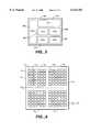
- FIG. 3is a diagram illustrating an integrated circuit chip including a plurality of macroblocks, and regions in which cells are to be placed by the present physical design automation system;
- FIG. 4is similar to FIG. 3, but illustrates a chip which is hierarchically partitioned into progressively smaller regions;
- FIG. 5is a diagram illustrating how cells which are placed by the present system can have different sizes and shapes
- FIG. 6is a diagram illustrating an initial assignment of a plurality of cells to a plurality of regions on a chip
- FIG. 7is a flowchart illustrating the process of the present invention.
- FIG. 8is a diagram illustrating computation of wirelength in an integrated circuit cell placement
- FIG. 9is a diagram illustrating how a cell is removed from a placement in accordance with the invention.
- FIGS. 10a and 10bare diagrams illustrating how the cell which was removed in FIG. 9 can be reassigned to two different regions and the wirelength computed for the two cases;
- FIG. 11is a diagram illustrating a two dimensional array of penalties for objects and regions
- FIG. 12is a flowchart illustrating an assignment process step of the present invention.
- FIG. 13is a diagram illustrating the construction of a normalized penalty scale
- FIGS. 14 and 15in combination illustrate the construction of a three dimensional array of normalized penalty summed values for subintervals
- FIG. 16is a diagram illustrating normalized penalties as assigned to subintervals of the normalized penalty scale
- FIG. 17is a diagram illustrating computation of a subinterval corresponding to a group size
- FIG. 18is a diagram illustrating a two dimensional array of cost function change values
- FIG. 19is a diagram illustrating movement of objects to produce a new assignment.
- FIG. 20is a graph illustrating computation of an optimum number of objects for movement.
- FIG. 1An exemplary integrated circuit chip is illustrated in FIG. 1 and generally designed by the reference numeral 10.
- the circuit 10includes a semiconductor substrate 12 on which are formed a number of functional circuit blocks that can have different sizes and shapes. Some are relatively large, such as a central processing unit (CPU) 14, a read-only memory (ROM) 16, a clock/timing unit 18, one or more random access memories (RAM) 20 and an input/output (I/O) interface unit 22. These blocks can be considered as modules for use in various circuit designs, and are represented as standard designs in circuit libraries.
- CPUcentral processing unit
- ROMread-only memory
- RAMrandom access memories
- I/Oinput/output
- the integrated circuit 10further comprises a large number, which can be tens of thousands, hundreds of thousands or even millions or more of small cells 24.
- Each cell 24represents a single logic element, such as a gate, or several logic elements that are interconnected in a standardized manner to perform a specific function. Cells 24 that consist of two or more interconnected gates or logic elements are also available as standard modules in circuit libraries.
- the cells 24 and the other elements of the circuit 10 described aboveare interconnected or routed in accordance with the logical design of the circuit to provide the desired functionality.
- the various elements of the circuit 10are interconnected by electrically conductive lines or traces that are routed, for example, through vertical channels 26 and horizontal channels 28 that run between the cells 24.
- FIG. 2illustrates an integrated circuit physical design automation system 30 for producing an optimized placement of the cells 24 such as illustrated in FIG. 1 in accordance with a method or process of the present invention.
- the system 30comprises a programmed digital computer 32 which may be of conventional type, including a processor such as a central processing Unit 34, a Read Only Memory (ROM) 36 for storing firmware, a Random Access Memory (RAM) 38 for storing an operating program and data, and an Input-Output (I/O) 40 for connecting the computer 32 to external devices.
- a processorsuch as a central processing Unit 34
- ROMRead Only Memory
- RAMRandom Access Memory
- I/OInput-Output
- the RAM 38stores an operating system 42 such as UNIX, and a physical design automation program and data 44 for implementing the process of the present invention.
- the system 30performs its function of physical design automation by causing the CPU 34 to execute the operating program 44 using input parameters specified by a user.
- FIG. 3illustrates one arrangement of regions in which cells are to be assigned or placed.
- An integrated circuit chip 50includes a plurality of fixed macroblocks 52a to 52c as described with reference to FIG. 1.
- the irregularly shaped area which is not covered by the macroblocks 52a to 52cis divided into rectangular cell regions 54a to 54g having different sizes and shapes.
- a large number of cells, which are not illustrated in FIG. 3,are to be assigned to the regions 54a to 54g.
- FIG. 4illustrates another arrangement of regions in which cells are to be assigned or placed.
- An integrated circuit chip 56has a single area in which a large number of cells are to be placed in a "Sea of Gates" configuration.
- the chip 56is hierarchically divided into a plurality of regions and subregions. For example, as illustrated, the chip 56 is initially divided into four regions R 1 to R 4 , which are in turn divided into four subregions.
- subregions R 1-1 to R 1-4 of the region R 1are shown in the drawing.
- the subregionscan themselves be subdivided into subregions, down to any number of levels.
- the subregion R 1-1is shown as being subdivided into four subregions R 1-1-1 to R 1-1-4 .
- the cell region 54a of FIG. 3can be hierarchically subdivided into subregions as illustrated in FIG. 4.
- the designation of regions in which cells, wiring segments, etc. are to be assignedis arbitrary, specified by the user, and is not limited to any particular configuration within the scope of the invention.
- cells which are to be assigned to regionscan have the same size and shape or, as illustrated, have different sizes and shapes.
- a region 60can have cells 62a to 62f having different heights and widths assigned to and placed therein.
- the present inventionprovides a process which is preferably implemented by a programmed digital computer for partitioning a large number, for example several hundred thousand or more, microelectronic device cells into a relatively small number of regions on an integrated circuit chip.
- the process of partitioninginvolves assigning individual cells to the regions of the chip such that a cost or penalty function, such as total wirelength of the placement, is minimized.
- a cost or penalty functionsuch as total wirelength of the placement
- the hypergraphrepresents the input data specifying the cells which are to be placed on the chip, and the wiring which interconnects the cells.
- the set O of vertices or objectsrepresents the set of cells
- the set Q of hyperedgesrepresents the wiring nets which interconnect the cells
- the sizes srepresent the sizes of the cells.
- the problemalso comprises specifying a set R of regions into which the cells are to be partitioned (assigned or mapped), and a set c of the sizes of the regions.
- the set R of regionsrepresents the regions or areas on the chip in which the cells are to be placed, and the set c of sizes represents the sizes or capacities of the regions for containing cells expressed as area, height or width.
- the present inventionsimultaneously partitions or assigns cells to all regions simultaneously, and therefore can be described as "multiway", as opposed to the prior art two way partitioning as represented by the min-cut algorithm.
- the steps of the present processare illustrated in FIG. 7.
- the first stepis to generate an initial placement either randomly, or using a methodology such as an optimization-driven placement technique as described in an article entitled "GORDIAN: VLSI Placement by Quadratic Programming and Slicing Optimization", by J. Kleinhans et al, IEEE Trans. on CAD, 1991, pp. 356-365.
- Another alternative for generating the initial placementis a force directed placement method.
- An initial partitioningcan be generated randomly, using a greedy algorithm such as min-cut, or using any other method as long as the capacities c j of the regions R j are not exceeded as indicated above.
- the next step of the processis to set a probability factor p equal to an initial value p o , and to set a number of iterations z equal to 0.
- a decision branchdetermines if z has reached a maximum value z max , indicating that the process has been performed a predetermined number (z max ) of times without changing the probability factor p. If z is less than z max , the value of z is incremented and the processes continues to the next step. If z has reached z max , z is reset to zero and the probability factor p is reduced by a factor of 2.
- the processdetermines if the probability factor p has been reduced below a minimum value p min . This represents an end criterion. If the probability factor p has not been reduced below p min , the process continues to the next step. If p has been reduced below p min , the process terminates.
- the set of all cellsis randomly divided into two subsets, a first subset V 1 of cells which remain on the chip, and a second subset V 2 of cells which are removed from the chip. Then, as will be described in detail below, penalties are computed for assigning each cell of the second subset V 2 to each region R j on the chip.
- the sizes or capacities c j of the regions from which the cells of the second subset V 2 were removedare recalculated such that their values are increased by the sizes s i of the removed cells.
- the cells of the second subset V 2are assigned to the regions R j on the chip such that a total penalty is minimized.
- Thisis preferably performed using an assignment method of the invention which will be described in detail below, but can alternatively be performed using a prior art algorithm such as the "Auction” or "Hungarian” algorithm.
- the Auction algorithmis described in, for example, a textbook entitled “Linear Network Optimization: Algorithms and Codes", by D. Bertsekas, MIT Press, Cambridge, Mass., 1991. pp. 167-243.
- the Hungarian algorithmis described in, for example, a textbook entitled “Network Programming”, by K. Murty, Prentice Hall, Englewood Cliffs, N.J., 1992, pp. 168-187.
- the processbranches back to the step of determining whether the value of z has increased above z max .
- an initial placementis generated, and the set of all cells is divided into a first subset of cells which remain on the chip, and a second subset of cells which are removed from the chip.
- the size of the second subsetis progressively reduced relative to the size of the first subset until an end criterion is reached.
- the process stepsare iteratively performed a number of times which is determined by incrementing the value of z from 0 to z max .
- the process steps which are iteratively performedcause randomly selected groups of cells to be "ripped up” and reassigned to different regions of the chip such that the total penalty is minimized. In this manner, the partitioning or assignment of the placement is iteratively improved until an optimal configuration is reached.
- the present methodcan be applied for improving an initial placement and partitioning including a fixed number of regions.
- an initial placementcan be hierarchically divided into progressively smaller regions as described above until a sufficiently fine level of detail is reached in which each cell is optimally placed in a region which does not contain any other cells.
- FIG. 7The process of FIG. 7 will now be described in detail with reference to FIGS. 8 to 20 of the drawings.
- total wirelength for each netcan be computed as rectilinear distances as illustrated in FIG. 8, which presents an exemplary set R of 16 regions R 1 to R 16 , and a set O of 6 cells O 1 to O 6 .
- the cells O 1 to O 6are placed in or assigned to the regions R 1 , R 3 , R 6 , R 9 , R 15 and R 16 respectively.
- a first net or hyperedge E 1interconnects the cells O 1 , O 3 , O 4 and O 5
- a second net E 2interconnects the cells O 2 , O 3 and O 6 .
- the cell O 3has connections to both nets E 1 and E 2 through different pins.
- the total wirelength ⁇ of a netcan be approximated as follows ##EQU2## where T is a subset of the regions R which contain cells of one net, (XB(j), YB(j)) are the X and Y coordinates of the center of the region R j , and (Xmed(T), Ymed(T) are X and Y coordinates of the median of the subset T.
- a medianis a value in an ordered set of values below and above which there is an equal number of values, or which is the arithmetic mean of the two middle values if there is no one middle value.
- the arithmetic meanwill not necessarily coincide with a center of a region. It is further within the scope of the invention to define a median interval between two middle values, consisting of the entire space between the middle values, and define any location within the median interval to be a median.
- one or the other of the middle valuescan be selected to represent the median. This will cause the median to coincide with the center of a region.
- the net E 1contains four cells, and the X coordinate of the median is between the centers of regions R 6 and R 9 which contain the cells O 3 and O 4 , with two cells being above and two cells being below the median. Similarly, the Y coordinate of the median of the net E 1 is between the centers of the regions R 1 and R 6 .
- a median M 1 of the net E 1will be defined at the center of the region R 10 , as corresponding to the X coordinate of the region R 6 which contains the cell O 3 , and the Y coordinate of the region R 9 which contains the cell O 4 .
- the net E 2has an odd number of values, and a median M 2 at the center of the region R 7 .
- the medians M 1 and M 2convert the hyperedges or nets E 1 and E 2 into rectilinear Steiner trees in which the medians M 1 and M 2 are single Steiner points.
- the Steiner pointscould be located at other points within a bounding box enclosing the nets and produce the same total wirelength.
- the total wirelength of the net E 1 as expressed aboveis the sum of the broken lines illustrated in FIG. 8, consisting of segments L 1 to L 6 having a total length of 6 units.
- the total wirelength of the net E 2is represented by the total length of solid line segments L 7 to L 10 having a total length of 5 units.
- ⁇is one-to-one mapping of the elements of V 2 to a set of integers that index V 2 , ⁇ :V 2 ⁇ 1 . . . b ⁇ , and ⁇ -1 its inverse mapping.
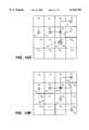
- FIGS. 9, 10a and 10billustrate how the penalty ⁇ * for a cell of the subset V 2 which is removed from a chip cell placement as described above with reference to FIG. 7 can be computed for assigning the cell to each region of the placement. It will be assumed that a cell O 1 has been removed, and that it is connected to a cell O 2 by a 2-pin net E 1 shown in broken line, and to cells O 2 , O 4 and O 5 by a 4-pin net E 2 shown in solid line.
- the cell O 1can be placed in or assigned to any of the regions R 1 to R 16 .
- a penalty ⁇ for assigning a cell to a regionis the total wirelength of all nets connected to the cell. This can be expressed as ⁇ :V 2 ⁇ R ⁇ , where ⁇ (i,j) is the penalty for placing the cell O i in the region R j .
- a total penalty ⁇ * for assigning a cell of the group V 2 to the regions Ris given as ##EQU3## where q is a subset of nets of Q which are connected to the cell O i , and intersects V 1 .
- the quantity ⁇ (i,j)is an initial condition which may or may not be specified along with the list of cells and the netlist. If no initial conditions are specified, this quantity is zero.
- FIG. 10aillustrates the penalty for assigning the cell O 1 to the region R 11 .
- the two pin net E 1has a total wirelength of 3 units.
- the net E 2has a median M, and a total wirelength of 4 units.
- FIG. 10billustrates the penalty for assigning the cell O 1 to the region R 16 .
- the wirelength of the net E 1is 5 units
- the wirelength of the net E 2is 7 units
- the penalty of placing the cell O 1 in the region R 11is smaller than placing it in the region R 16 .
- the new available capacity c j of a region R jis the initial capacity of the region decreased by the areas of cells already assigned to the region, and can be expressed as
- a cost function ⁇ for the placement resulting from re-assigning the cells of the second subset V 2 to the regions R jis computed as ##EQU4## where F(q) is the set of all regions into which the cells connected to the set of nets q are assigned, and F(i) is the set of regions into which the cells are mapped.
- the first term on the right side of the above equationis the total wirelength of the placement after assigning the cells of the subset V 2 to the regions.
- the second term on the rightis the total penalty of the re-assigned cells.
- the present inventioncan be practiced using either or both of these terms.
- the inventioncan be practiced using a cost function which does not include either of these terms. Regardless of which cost function is used to determine the quality of the partitioning, the object of the process is to find the assignment for which the cost is minimized.
- the assignment problem for assigning the cells of the subset V 2is to find the mapping F * of the set of vertices V 2 to the set of regions R, such that
- penalties ⁇are specified for assigning each cell of the subset V 2 to each region R j as described above.
- a penaltycan be considered as a negative affinity, with the affinity being an attractive force determined by a conventional force directed placement algorithm based on a model of masses and springs.
- the number n of cells O i , sizes s i of cells O, number m of regions R j , capacities c j of regions m, and penalties ⁇ (i,j) for assigning the cell O i to region R jare specified by the user as a two dimensional array having the form illustrated in FIG. 11.
- the capacity c j of a region R jis the size (area) of the region which is available to have cells placed therein.
- FIG. 12is a flowchart illustrating the main process steps of the assignment methodology. The following detailed description will be presented within the framework of the flowchart.
- the generalized assignment problemcan be formulated as follows.
- the cost function of the assignment Fis equal to the total penalty: ##EQU6## The goal is to find the assignment F with the minimal COST(F).
- Normalized penalties ⁇ (i,j)are computed by dividing the penalties ⁇ (i,j) by the sizes of the cells as ##EQU7##
- the normalized penalty change scaleis specified as having a minimum (most negative) value -M and a maximum (most positive) value +M, where
- the quantity ⁇is the "accuracy factor", and is selected in accordance with the characteristics of the computer on which the design automation program is run. Smaller values of ⁇ will result in greater accuracy and longer computing time, and vice-versa. It will be further noted that the last subinterval I k can have a value of less than ⁇ .
- the next step of the present processis to construct an initial permissible assignment which is to be improved upon by the invention.
- the initial assignmentcan be generated randomly, or by using another algorithm.
- the constraint which must be satisfiedis, as set forth above, that for each region, the sum of sizes of all cells assigned to that region is not greater than the capacity of the region.
- Lan initial value is assigned to L.
- the preferred initial value of Lis T, although the invention is not so limited.
- the initial value of V LV T .
- the present inventionproduces a rapid improvement in the initial assignment (and iteratively improved versions thereof) by moving the maximum number of cells between regions which will produce a maximum reduction in the cost of the assignment. This is done by moving the selected number of cells which have the largest negative normalized penalty changes through a complete permutation of the regions.
- region capacitieswill be exceeded upon completion of a permutation because the same number of cells is removed from and returned to each region. Although region capacities can be exceeded at intermediate stages of permutations, this does not affect the result of the process.
- An cellis in a subinterval if its normalized penalty change ⁇ , when the object is moved from j 1 to j 2 , has a value within the subinterval.
- the arraycan be expressed as:
- ris an index for the subintervals
- FIGS. 14 and 15illustrate the array ⁇ (r,j 1 j 2 ), where FIG. 14 represents a two dimensional portion of the array for a given value of r, and FIG. 15 represents a one dimensional portion of the array for given values of j 1 and j 2 . There are m(m-1) non-trivial values of ⁇ .
- Each value of xis equal to the maximal number of subintervals I r which contain cells having a total size no greater than V L for each respective value of V L , and each pair j 1 , j 2 .
- FIG. 16illustrates an example of the computation of the values of x for one pair j 1 ,j 2 . It will be assumed that MAX
- the subinterval I 1includes two cells O 23 and O 4 having normalized penalty changes ⁇ of -194 and -192, and sizes s of 4 and 5 respectively.
- the subinterval I 2contains one cell O 18
- the subinterval I 3contains one cell O 31
- the subinterval I 4contains no cells
- the subinterval I 5contains three cells
- the subinterval I 6contains one cell.
- the total group size V 532.
- the subintervals I 1 -I 6contain cells having a total size of 34.
- each elementrepresents the change in total cost function created by moving cells having total size V L between the corresponding two regions.
- FIG. 17further illustrates how the effect is equal to the product of the total cell size and the value of the subinterval.
- EFFECTis obtained by summing the individual values of ⁇ for each move, with a value of EFFECT being computed for each possible permutation.
- the optimal permutationis the one with the highest negative value of EFFECT (negative change corresponds to reduction of cost function).
- the value of Lis then decremented, and the process is repeated for the next lowest value of V L .
- the goalis to determine the highest value of L which will produce an increasing reduction of cost function. If the lower value of L produces a more negative value of EFFECT, the value of L is decremented again until the new lower value produces a less negative value of EFFECT. This is expressed mathematically as:
- V orepresent the current optimal value of V L . It will be seen that the value of EFFECT varies approximately parabolically with V L , and the value of V o produces a maximum negative value MAX NEG of EFFECT. A higher value V o +1 produces a more positive value of EFFECT, as does a more negative value V 0 -1.
- the cells for movementare selected by determining a subinterval r for each cell as
- a random number generator or the like(not shown) is used to generate numbers with a probability equal to that above value that the numbers will have values greater than a predetermined value.
- a random numberis generated for each cell in the subinterval x+1. If the random number is larger than the predetermined value, the cell is moved. If the random number is smaller than the predetermined value, the cell is not moved.
- the processbranches back as illustrated in FIG. 12 to determine a new optimal permutation for the modified assignment which may or may not have a decremented value of L.
- the present inventionsolves the partitioning problem and the problem of placing the partitions on the chip simultaneously, therefore overcoming the drawbacks of the prior art. This is accomplished by concurrently assigning cells to more than two regions (multiway), as compared to only two regions (bipartitioning) as in the prior art.
- the present inventionis also capable of improving on an initial partitioning or assignment produced using a min-cut or other methodology, and can also be considered as a placement improvement process.
- the present inventionyet further overcomes the limitations of the prior art in that it is capable of operating on cells of different sizes and shapes.
- the complexity of the present process where implemented on a digital computeris linear, thereby producing results with greatly reduced run times as compared to the prior art.
Landscapes
- Engineering & Computer Science (AREA)
- Computer Hardware Design (AREA)
- Physics & Mathematics (AREA)
- Theoretical Computer Science (AREA)
- Architecture (AREA)
- Evolutionary Computation (AREA)
- Geometry (AREA)
- General Engineering & Computer Science (AREA)
- General Physics & Mathematics (AREA)
- Design And Manufacture Of Integrated Circuits (AREA)
Abstract
Description
______________________________________ H hypergraph Q.sub.h net h index for net q subset of nets connected to a cell T subset of regions containing cells of one net O.sub.i cell (object or vertex) i index for cell n number of cells s.sub.i size of cell R.sub.j region j index for region m number of regions c.sub.j capacity of region ψ penalty Ψ normalized penalty ΔΨ normalized penalty change F assignment p permutation I.sub.r subinterval r index for subinterval k number of subintervals x subinterval corresponding to V.sub.L δ accuracy parameter M maximum normalized penalty V.sub.L group size L index for group size V.sub.T maximum group size V.sub.o optimal group size C group size constant total size of objects in subinterval Ω change of cost function for moving V.sub.L group ______________________________________ size
O=V.sub.1 ∪V.sub.2 and V.sub.1 ∩V.sub.2 =.o slashed.
c.sup.* (j)=c(j)-|i |F(i)-j∩V.sub.1 |
∀j:|{i|iεV.sub.2,(F.sup.* (i)=j)}|≦c.sup.* (j)M=2×MAX|Ψ(i,j)|
λ(r,j.sub.1,j.sub.2)=Σs.sub.i
i,F(i)=j.sub.i, (Ψ(i,j.sub.2)=Ψ(i,j.sub.1))εI.sub.I
ΔΨ=Ψ(i,j.sub.2)-Ψ(i,j.sub.1)
p:{1,2 . . . m}→{1,2 . . . m}EFFECT(p.sub.1,V.sub.L)<EFFECT(p.sub.2,V.sub.L-1)
(Ψ(i,j.sub.2)-Ψ(i,j.sub.1))εI.sub.r
Claims (22)
Priority Applications (1)
| Application Number | Priority Date | Filing Date | Title |
|---|---|---|---|
| US08/991,419US6134702A (en) | 1997-12-16 | 1997-12-16 | Physical design automation system and process for designing integrated circuit chips using multiway partitioning with constraints |
Applications Claiming Priority (1)
| Application Number | Priority Date | Filing Date | Title |
|---|---|---|---|
| US08/991,419US6134702A (en) | 1997-12-16 | 1997-12-16 | Physical design automation system and process for designing integrated circuit chips using multiway partitioning with constraints |
Publications (1)
| Publication Number | Publication Date |
|---|---|
| US6134702Atrue US6134702A (en) | 2000-10-17 |
Family
ID=25537198
Family Applications (1)
| Application Number | Title | Priority Date | Filing Date |
|---|---|---|---|
| US08/991,419Expired - LifetimeUS6134702A (en) | 1997-12-16 | 1997-12-16 | Physical design automation system and process for designing integrated circuit chips using multiway partitioning with constraints |
Country Status (1)
| Country | Link |
|---|---|
| US (1) | US6134702A (en) |
Cited By (43)
| Publication number | Priority date | Publication date | Assignee | Title |
|---|---|---|---|---|
| US20020069397A1 (en)* | 2000-12-06 | 2002-06-06 | Steven Teig | Method and apparatus for placing circuit modules |
| US20020100007A1 (en)* | 2000-12-06 | 2002-07-25 | Steven Teig | Recursive partitioning placement method and apparatus |
| US20020157075A1 (en)* | 2000-12-06 | 2002-10-24 | Steven Teig | Method and apparatus for computing placement costs |
| US20020170027A1 (en)* | 2000-12-06 | 2002-11-14 | Steven Teig | Method and apparatus for pre-computing placement costs |
| US20020199165A1 (en)* | 2000-12-06 | 2002-12-26 | Steven Teig | Method and apparatus for pre-computing attributes of routes |
| US6543039B1 (en)* | 1998-09-29 | 2003-04-01 | Kabushiki Kaisha Toshiba | Method of designing integrated circuit and apparatus for designing integrated circuit |
| US20030066042A1 (en)* | 2001-08-23 | 2003-04-03 | Steven Teig | Routing method and apparatus |
| US20030064559A1 (en)* | 2001-08-23 | 2003-04-03 | Steven Teig | Method and apparatus for generating routes for groups of related node configurations |
| US20030088841A1 (en)* | 2000-12-06 | 2003-05-08 | Steven Teig | Partitioning placement method and apparatus |
| US6577992B1 (en)* | 1999-05-07 | 2003-06-10 | Nassda Corporation | Transistor level circuit simulator using hierarchical data |
| US6671864B2 (en) | 2000-12-06 | 2003-12-30 | Cadence Design Systems, Inc. | Method and apparatus for using a diagonal line to measure an attribute of a bounding box of a net |
| US6738960B2 (en) | 2001-01-19 | 2004-05-18 | Cadence Design Systems, Inc. | Method and apparatus for producing sub-optimal routes for a net by generating fake configurations |
| US20040098697A1 (en)* | 2002-11-18 | 2004-05-20 | Jonathan Frankle | Method and apparatus for routing with independent goals on different layers |
| US20040098696A1 (en)* | 2002-11-18 | 2004-05-20 | Steven Teig | Method and apparatus for routing |
| US20040098680A1 (en)* | 2002-11-18 | 2004-05-20 | Steven Teig | Method and apparatus for searching for a three-dimensional global path |
| US20040098694A1 (en)* | 2002-11-18 | 2004-05-20 | Steven Teig | Method and apparatus for routing |
| US20040098698A1 (en)* | 2002-11-18 | 2004-05-20 | Steven Teig | Method and apparatus for searching for a global path |
| US20040098695A1 (en)* | 2002-11-18 | 2004-05-20 | Steven Teig | Method and apparatus for routing |
| US20040098691A1 (en)* | 2002-11-18 | 2004-05-20 | Steven Teig | Method and apparatus for performing an exponential path search |
| US20040103387A1 (en)* | 2002-11-18 | 2004-05-27 | Steven Teig | Method and apparatus for computing capacity of a region for non-manhattan routing |
| US6745379B2 (en) | 2001-08-23 | 2004-06-01 | Cadence Design Systems, Inc. | Method and apparatus for identifying propagation for routes with diagonal edges |
| US6862722B2 (en) | 2002-12-20 | 2005-03-01 | Taiwan Semiconductor Manufacturing Co., Ltd. | Extendable method for revising patterned microelectronic conductor layer layouts |
| US20050086624A1 (en)* | 2003-10-17 | 2005-04-21 | Lsi Logic Corporation | Process and apparatus for fast assignment of objects to a rectangle |
| US20050091625A1 (en)* | 2003-10-27 | 2005-04-28 | Lsi Logic Corporation | Process and apparatus for placement of cells in an IC during floorplan creation |
| US20050125756A1 (en)* | 2003-12-03 | 2005-06-09 | International Business Machines Corporation | Autonomic graphical partitioning |
| US6951006B1 (en)* | 2002-01-22 | 2005-09-27 | Cadence Design Systems, Inc. | Decomposing IC regions and embedding routes |
| US20050216870A1 (en)* | 2004-03-26 | 2005-09-29 | International Business Machines Corporation | Ic design density checking method, system and program product |
| US6957410B2 (en) | 2000-12-07 | 2005-10-18 | Cadence Design Systems, Inc. | Method and apparatus for adaptively selecting the wiring model for a design region |
| US7003754B2 (en) | 2000-12-07 | 2006-02-21 | Cadence Design Systems, Inc. | Routing method and apparatus that use of diagonal routes |
| US7013445B1 (en) | 2002-12-31 | 2006-03-14 | Cadence Design Systems, Inc. | Post processor for optimizing manhattan integrated circuits placements into non manhattan placements |
| US7058913B1 (en) | 2001-09-06 | 2006-06-06 | Cadence Design Systems, Inc. | Analytical placement method and apparatus |
| US7073150B2 (en) | 2000-12-07 | 2006-07-04 | Cadence Design Systems, Inc. | Hierarchical routing method and apparatus that use diagonal routes |
| US7089519B1 (en) | 2002-12-31 | 2006-08-08 | Cadence Design System, Inc. | Method and system for performing placement on non Manhattan semiconductor integrated circuits |
| US7103865B2 (en) | 2003-11-21 | 2006-09-05 | Lsi Logic Corporation | Process and apparatus for placement of megacells in ICs design |
| US7103858B2 (en) | 2004-04-14 | 2006-09-05 | Lsi Logic Corporation | Process and apparatus for characterizing intellectual property for integration into an IC platform environment |
| US7137097B1 (en) | 2002-08-27 | 2006-11-14 | Sun Microsystems, Inc. | Constraint-based global router for routing high performance designs |
| US7143382B2 (en) | 2001-08-23 | 2006-11-28 | Cadence Design Systems, Inc. | Method and apparatus for storing routes |
| US7149993B1 (en)* | 2004-03-29 | 2006-12-12 | Xilinx, Inc. | Method, system, and apparatus for incremental design in programmable logic devices using floorplanning |
| US7398498B2 (en) | 2001-08-23 | 2008-07-08 | Cadence Design Systems, Inc. | Method and apparatus for storing routes for groups of related net configurations |
| US7506295B1 (en) | 2002-12-31 | 2009-03-17 | Cadence Design Systems, Inc. | Non manhattan floor plan architecture for integrated circuits |
| US20090293034A1 (en)* | 2006-09-15 | 2009-11-26 | Pai Ravi R | Method and system for processing geometrical layout design data |
| US20130191805A1 (en)* | 2012-01-06 | 2013-07-25 | Mentor Graphics Corporation | Simulation Of Circuits With Repetitive Elements |
| EP4286942A3 (en)* | 2022-06-03 | 2023-12-13 | Samsung Electronics Co., Ltd. | Extreme ultraviolet lithography device and method of operating extreme ultraviolet lithography device |
Citations (1)
| Publication number | Priority date | Publication date | Assignee | Title |
|---|---|---|---|---|
| US5699265A (en)* | 1995-09-08 | 1997-12-16 | Lsi Logic Corporation | Physical design automation system and process for designing integrated circuit chips using multiway partitioning with constraints |
- 1997
- 1997-12-16USUS08/991,419patent/US6134702A/ennot_activeExpired - Lifetime
Patent Citations (1)
| Publication number | Priority date | Publication date | Assignee | Title |
|---|---|---|---|---|
| US5699265A (en)* | 1995-09-08 | 1997-12-16 | Lsi Logic Corporation | Physical design automation system and process for designing integrated circuit chips using multiway partitioning with constraints |
Cited By (90)
| Publication number | Priority date | Publication date | Assignee | Title |
|---|---|---|---|---|
| US6543039B1 (en)* | 1998-09-29 | 2003-04-01 | Kabushiki Kaisha Toshiba | Method of designing integrated circuit and apparatus for designing integrated circuit |
| US6993728B2 (en) | 1998-09-29 | 2006-01-31 | Kabushiki Kaisha Toshiba | Method of designing integrated circuit and apparatus for designing integrated circuit |
| US6577992B1 (en)* | 1999-05-07 | 2003-06-10 | Nassda Corporation | Transistor level circuit simulator using hierarchical data |
| US20040123260A1 (en)* | 2000-12-06 | 2004-06-24 | Steven Teig | Method and Apparatus for Pre-computing and Using Multiple Placement Cost Attributes to Quantify the Quality of a Placement a Configuration within a Partitioned Region |
| US6907593B2 (en) | 2000-12-06 | 2005-06-14 | Cadence Design Systems, Inc. | Method and apparatus for pre-computing attributes of routes |
| US20020199165A1 (en)* | 2000-12-06 | 2002-12-26 | Steven Teig | Method and apparatus for pre-computing attributes of routes |
| US20020157075A1 (en)* | 2000-12-06 | 2002-10-24 | Steven Teig | Method and apparatus for computing placement costs |
| US7013450B2 (en) | 2000-12-06 | 2006-03-14 | Cadence Design Systems, Inc. | Method and apparatus for routing |
| US20020100007A1 (en)* | 2000-12-06 | 2002-07-25 | Steven Teig | Recursive partitioning placement method and apparatus |
| US20030088841A1 (en)* | 2000-12-06 | 2003-05-08 | Steven Teig | Partitioning placement method and apparatus |
| US20020124231A1 (en)* | 2000-12-06 | 2002-09-05 | Steven Teig | Method and apparatus for pre-computing and using placement costs within a partitioned region for multiple wiring models |
| US6651233B2 (en)* | 2000-12-06 | 2003-11-18 | Cadence Design Systems, Inc. | Method and apparatus for measuring congestion in a partitioned region |
| US6802049B2 (en) | 2000-12-06 | 2004-10-05 | Cadence Design Systems, Inc. | Method and apparatus for computing placement costs by calculating bend values of connection graphs that model interconnect line topologies |
| US7024650B2 (en) | 2000-12-06 | 2006-04-04 | Cadence Design Systems, Inc. | Method and apparatus for considering diagonal wiring in placement |
| US6988256B2 (en)* | 2000-12-06 | 2006-01-17 | Cadence Design Systems, Inc. | Method and apparatus for pre-computing and using multiple placement cost attributes to quantify the quality of a placement configuration within a partitioned region |
| US20060010412A1 (en)* | 2000-12-06 | 2006-01-12 | Steven Teig | Method and Apparatus for Using Connection Graphs with Potential Diagonal Edges to Model Interconnect Topologies During Placement |
| US6952815B2 (en) | 2000-12-06 | 2005-10-04 | Cadence Design Systems, Inc. | Probabilistic routing method and apparatus |
| US7055120B2 (en) | 2000-12-06 | 2006-05-30 | Cadence Design Systems, Inc. | Method and apparatus for placing circuit modules |
| US6910198B2 (en) | 2000-12-06 | 2005-06-21 | Cadence Design Systems, Inc. | Method and apparatus for pre-computing and using placement costs within a partitioned region for multiple wiring models |
| US6904580B2 (en) | 2000-12-06 | 2005-06-07 | Cadence Design Systems, Inc. | Method and apparatus for pre-computing placement costs |
| US7080336B2 (en) | 2000-12-06 | 2006-07-18 | Cadence Design Systems, Inc. | Method and apparatus for computing placement costs |
| US7089523B2 (en) | 2000-12-06 | 2006-08-08 | Cadence Design Systems, Inc. | Method and apparatus for using connection graphs with potential diagonal edges to model interconnect topologies during placement |
| US20020069397A1 (en)* | 2000-12-06 | 2002-06-06 | Steven Teig | Method and apparatus for placing circuit modules |
| US7100137B2 (en) | 2000-12-06 | 2006-08-29 | Cadence Design Systems, Inc. | Method and apparatus for quantifying the quality of placement configurations in a partitioned region of an integrated circuit layout |
| US6848091B2 (en) | 2000-12-06 | 2005-01-25 | Cadence Design Systems, Inc. | Partitioning placement method and apparatus |
| US20020170027A1 (en)* | 2000-12-06 | 2002-11-14 | Steven Teig | Method and apparatus for pre-computing placement costs |
| US6678872B2 (en) | 2000-12-06 | 2004-01-13 | Cadence Design Systems, Inc. | Method and apparatus for using a diagonal line to measure congestion in a region of an integrated-circuit layout |
| US6671864B2 (en) | 2000-12-06 | 2003-12-30 | Cadence Design Systems, Inc. | Method and apparatus for using a diagonal line to measure an attribute of a bounding box of a net |
| US6826737B2 (en) | 2000-12-06 | 2004-11-30 | Cadence Design Systems, Inc. | Recursive partitioning placement method and apparatus |
| US7003754B2 (en) | 2000-12-07 | 2006-02-21 | Cadence Design Systems, Inc. | Routing method and apparatus that use of diagonal routes |
| US6957410B2 (en) | 2000-12-07 | 2005-10-18 | Cadence Design Systems, Inc. | Method and apparatus for adaptively selecting the wiring model for a design region |
| US7073150B2 (en) | 2000-12-07 | 2006-07-04 | Cadence Design Systems, Inc. | Hierarchical routing method and apparatus that use diagonal routes |
| US7139994B2 (en) | 2001-01-19 | 2006-11-21 | Cadence Design Systems, Inc. | Method and apparatus for pre-computing routes |
| US7096448B2 (en) | 2001-01-19 | 2006-08-22 | Cadence Design Systems, Inc. | Method and apparatus for diagonal routing by using several sets of lines |
| US6687893B2 (en) | 2001-01-19 | 2004-02-03 | Cadence Design Systems, Inc. | Method and apparatus for pre-computing routes for multiple wiring models |
| US6915501B2 (en) | 2001-01-19 | 2005-07-05 | Cadence Design Systems, Inc. | LP method and apparatus for identifying routes |
| US6738960B2 (en) | 2001-01-19 | 2004-05-18 | Cadence Design Systems, Inc. | Method and apparatus for producing sub-optimal routes for a net by generating fake configurations |
| US6883154B2 (en) | 2001-01-19 | 2005-04-19 | Cadence Design Systems, Inc. | LP method and apparatus for identifying route propagations |
| US6795958B2 (en) | 2001-08-23 | 2004-09-21 | Cadence Design Systems, Inc. | Method and apparatus for generating routes for groups of related node configurations |
| US6877149B2 (en) | 2001-08-23 | 2005-04-05 | Cadence Design Systems, Inc. | Method and apparatus for pre-computing routes |
| US7143382B2 (en) | 2001-08-23 | 2006-11-28 | Cadence Design Systems, Inc. | Method and apparatus for storing routes |
| US6931616B2 (en) | 2001-08-23 | 2005-08-16 | Cadence Design Systems, Inc. | Routing method and apparatus |
| US20030066042A1 (en)* | 2001-08-23 | 2003-04-03 | Steven Teig | Routing method and apparatus |
| US7398498B2 (en) | 2001-08-23 | 2008-07-08 | Cadence Design Systems, Inc. | Method and apparatus for storing routes for groups of related net configurations |
| US6745379B2 (en) | 2001-08-23 | 2004-06-01 | Cadence Design Systems, Inc. | Method and apparatus for identifying propagation for routes with diagonal edges |
| US20030064559A1 (en)* | 2001-08-23 | 2003-04-03 | Steven Teig | Method and apparatus for generating routes for groups of related node configurations |
| US7155697B2 (en) | 2001-08-23 | 2006-12-26 | Cadence Design Systems, Inc. | Routing method and apparatus |
| US7493581B2 (en) | 2001-09-06 | 2009-02-17 | Cadence Design Systems, Inc. | Analytical placement method and apparatus |
| US7058913B1 (en) | 2001-09-06 | 2006-06-06 | Cadence Design Systems, Inc. | Analytical placement method and apparatus |
| US6951006B1 (en)* | 2002-01-22 | 2005-09-27 | Cadence Design Systems, Inc. | Decomposing IC regions and embedding routes |
| US7137097B1 (en) | 2002-08-27 | 2006-11-14 | Sun Microsystems, Inc. | Constraint-based global router for routing high performance designs |
| US20040098691A1 (en)* | 2002-11-18 | 2004-05-20 | Steven Teig | Method and apparatus for performing an exponential path search |
| US20040103387A1 (en)* | 2002-11-18 | 2004-05-27 | Steven Teig | Method and apparatus for computing capacity of a region for non-manhattan routing |
| US7010771B2 (en) | 2002-11-18 | 2006-03-07 | Cadence Design Systems, Inc. | Method and apparatus for searching for a global path |
| US6996789B2 (en) | 2002-11-18 | 2006-02-07 | Cadence Design Systems, Inc. | Method and apparatus for performing an exponential path search |
| US8112733B2 (en) | 2002-11-18 | 2012-02-07 | Cadence Design Systems, Inc. | Method and apparatus for routing with independent goals on different layers |
| US6988257B2 (en) | 2002-11-18 | 2006-01-17 | Cadence Design Systems, Inc. | Method and apparatus for routing |
| US20040098697A1 (en)* | 2002-11-18 | 2004-05-20 | Jonathan Frankle | Method and apparatus for routing with independent goals on different layers |
| US7047513B2 (en) | 2002-11-18 | 2006-05-16 | Cadence Design Systems, Inc. | Method and apparatus for searching for a three-dimensional global path |
| US7480885B2 (en) | 2002-11-18 | 2009-01-20 | Cadence Design Systems, Inc. | Method and apparatus for routing with independent goals on different layers |
| US20040098696A1 (en)* | 2002-11-18 | 2004-05-20 | Steven Teig | Method and apparatus for routing |
| US7003752B2 (en) | 2002-11-18 | 2006-02-21 | Cadence Design Systems, Inc. | Method and apparatus for routing |
| US7171635B2 (en) | 2002-11-18 | 2007-01-30 | Cadence Design Systems, Inc. | Method and apparatus for routing |
| US7080342B2 (en) | 2002-11-18 | 2006-07-18 | Cadence Design Systems, Inc | Method and apparatus for computing capacity of a region for non-Manhattan routing |
| US20040098680A1 (en)* | 2002-11-18 | 2004-05-20 | Steven Teig | Method and apparatus for searching for a three-dimensional global path |
| US20040098694A1 (en)* | 2002-11-18 | 2004-05-20 | Steven Teig | Method and apparatus for routing |
| US20040098698A1 (en)* | 2002-11-18 | 2004-05-20 | Steven Teig | Method and apparatus for searching for a global path |
| US20040098695A1 (en)* | 2002-11-18 | 2004-05-20 | Steven Teig | Method and apparatus for routing |
| US20050132315A1 (en)* | 2002-12-20 | 2005-06-16 | Taiwan Semiconductor Manufacturing Co., Ltd. | Extendable method for revising patterned microelectronic conductor layer layouts |
| US6862722B2 (en) | 2002-12-20 | 2005-03-01 | Taiwan Semiconductor Manufacturing Co., Ltd. | Extendable method for revising patterned microelectronic conductor layer layouts |
| US7013445B1 (en) | 2002-12-31 | 2006-03-14 | Cadence Design Systems, Inc. | Post processor for optimizing manhattan integrated circuits placements into non manhattan placements |
| US7506295B1 (en) | 2002-12-31 | 2009-03-17 | Cadence Design Systems, Inc. | Non manhattan floor plan architecture for integrated circuits |
| US7089519B1 (en) | 2002-12-31 | 2006-08-08 | Cadence Design System, Inc. | Method and system for performing placement on non Manhattan semiconductor integrated circuits |
| US7111264B2 (en)* | 2003-10-17 | 2006-09-19 | Lsi Logic Corporation | Process and apparatus for fast assignment of objects to a rectangle |
| US20050086624A1 (en)* | 2003-10-17 | 2005-04-21 | Lsi Logic Corporation | Process and apparatus for fast assignment of objects to a rectangle |
| US7036102B2 (en)* | 2003-10-27 | 2006-04-25 | Lsi Logic Corporation | Process and apparatus for placement of cells in an IC during floorplan creation |
| US20050091625A1 (en)* | 2003-10-27 | 2005-04-28 | Lsi Logic Corporation | Process and apparatus for placement of cells in an IC during floorplan creation |
| US7103865B2 (en) | 2003-11-21 | 2006-09-05 | Lsi Logic Corporation | Process and apparatus for placement of megacells in ICs design |
| US7051307B2 (en) | 2003-12-03 | 2006-05-23 | International Business Machines Corporation | Autonomic graphical partitioning |
| US20050125756A1 (en)* | 2003-12-03 | 2005-06-09 | International Business Machines Corporation | Autonomic graphical partitioning |
| US20050216870A1 (en)* | 2004-03-26 | 2005-09-29 | International Business Machines Corporation | Ic design density checking method, system and program product |
| US7093212B2 (en) | 2004-03-26 | 2006-08-15 | International Business Machines Corporation | IC design density checking method, system and program product |
| US7149993B1 (en)* | 2004-03-29 | 2006-12-12 | Xilinx, Inc. | Method, system, and apparatus for incremental design in programmable logic devices using floorplanning |
| US7103858B2 (en) | 2004-04-14 | 2006-09-05 | Lsi Logic Corporation | Process and apparatus for characterizing intellectual property for integration into an IC platform environment |
| US20090293034A1 (en)* | 2006-09-15 | 2009-11-26 | Pai Ravi R | Method and system for processing geometrical layout design data |
| US7823110B2 (en)* | 2006-09-15 | 2010-10-26 | Softjin Technologies Private Limited | Method and system for processing geometrical layout design data |
| US20130191805A1 (en)* | 2012-01-06 | 2013-07-25 | Mentor Graphics Corporation | Simulation Of Circuits With Repetitive Elements |
| US8832635B2 (en)* | 2012-01-06 | 2014-09-09 | Mentor Graphics Corporation | Simulation of circuits with repetitive elements |
| EP4286942A3 (en)* | 2022-06-03 | 2023-12-13 | Samsung Electronics Co., Ltd. | Extreme ultraviolet lithography device and method of operating extreme ultraviolet lithography device |
| US11960212B2 (en) | 2022-06-03 | 2024-04-16 | Samsung Electronics Co., Ltd. | Extreme ultraviolet lithography device and method of operating extreme ultraviolet lithography device |
Similar Documents
| Publication | Publication Date | Title |
|---|---|---|
| US6134702A (en) | Physical design automation system and process for designing integrated circuit chips using multiway partitioning with constraints | |
| US5699265A (en) | Physical design automation system and process for designing integrated circuit chips using multiway partitioning with constraints | |
| US5638293A (en) | Optimal pad location method for microelectronic circuit cell placement | |
| US5712793A (en) | Physical design automation system and process for designing integrated circuit chips using fuzzy cell clusterization | |
| US5909376A (en) | Physical design automation system and process for designing integrated circuit chips using highly parallel sieve optimization with multiple "jiggles" | |
| US5661663A (en) | Physical design automation system and method using hierarchical clusterization and placement improvement based on complete re-placement of cell clusters | |
| US5745363A (en) | Optimization processing for integrated circuit physical design automation system using optimally switched cost function computations | |
| US5914887A (en) | Congestion based cost factor computing apparatus for integrated circuit physical design automation system | |
| US6493658B1 (en) | Optimization processing for integrated circuit physical design automation system using optimally switched fitness improvement algorithms | |
| US5557533A (en) | Cell placement alteration apparatus for integrated circuit chip physical design automation system | |
| US5875117A (en) | Simultaneous placement and routing (SPAR) method for integrated circuit physical design automation system | |
| US5682322A (en) | Optimization processing for integrated circuit physical design automation system using chaotic fitness improvement method | |
| US6155725A (en) | Cell placement representation and transposition for integrated circuit physical design automation system | |
| US5963975A (en) | Single chip integrated circuit distributed shared memory (DSM) and communications nodes | |
| US5898597A (en) | Integrated circuit floor plan optimization system | |
| US5870313A (en) | Optimization processing for integrated circuit physical design automation system using parallel moving windows | |
| US6651235B2 (en) | Scalable, partitioning integrated circuit layout system | |
| US6223332B1 (en) | Advanced modular cell placement system with overlap remover with minimal noise | |
| US5815403A (en) | Fail-safe distributive processing method for producing a highest fitness cell placement for an integrated circuit chip | |
| US5835378A (en) | Computer implemented method for leveling interconnect wiring density in a cell placement for an integrated circuit chip | |
| US6038385A (en) | Physical design automation system and process for designing integrated circuit chip using "chessboard" and "jiggle" optimization | |
| US5838585A (en) | Physical design automation system and method using monotonically improving linear clusterization | |
| US5796625A (en) | Physical design automation system and process for designing integrated circuit chip using simulated annealing with "chessboard and jiggle" optimization | |
| US5831863A (en) | Advanced modular cell placement system with wire length driven affinity system | |
| US5870312A (en) | Advanced modular cell placement system with dispersion-driven levelizing system |
Legal Events
| Date | Code | Title | Description |
|---|---|---|---|
| STCF | Information on status: patent grant | Free format text:PATENTED CASE | |
| FPAY | Fee payment | Year of fee payment:4 | |
| FEPP | Fee payment procedure | Free format text:PAYOR NUMBER ASSIGNED (ORIGINAL EVENT CODE: ASPN); ENTITY STATUS OF PATENT OWNER: LARGE ENTITY Free format text:PAYER NUMBER DE-ASSIGNED (ORIGINAL EVENT CODE: RMPN); ENTITY STATUS OF PATENT OWNER: LARGE ENTITY | |
| FPAY | Fee payment | Year of fee payment:8 | |
| FPAY | Fee payment | Year of fee payment:12 | |
| AS | Assignment | Owner name:DEUTSCHE BANK AG NEW YORK BRANCH, AS COLLATERAL AG Free format text:PATENT SECURITY AGREEMENT;ASSIGNORS:LSI CORPORATION;AGERE SYSTEMS LLC;REEL/FRAME:032856/0031 Effective date:20140506 | |
| AS | Assignment | Owner name:AVAGO TECHNOLOGIES GENERAL IP (SINGAPORE) PTE. LTD Free format text:ASSIGNMENT OF ASSIGNORS INTEREST;ASSIGNOR:LSI CORPORATION;REEL/FRAME:035390/0388 Effective date:20140814 | |
| AS | Assignment | Owner name:AGERE SYSTEMS LLC, PENNSYLVANIA Free format text:TERMINATION AND RELEASE OF SECURITY INTEREST IN PATENT RIGHTS (RELEASES RF 032856-0031);ASSIGNOR:DEUTSCHE BANK AG NEW YORK BRANCH, AS COLLATERAL AGENT;REEL/FRAME:037684/0039 Effective date:20160201 Owner name:LSI CORPORATION, CALIFORNIA Free format text:TERMINATION AND RELEASE OF SECURITY INTEREST IN PATENT RIGHTS (RELEASES RF 032856-0031);ASSIGNOR:DEUTSCHE BANK AG NEW YORK BRANCH, AS COLLATERAL AGENT;REEL/FRAME:037684/0039 Effective date:20160201 | |
| AS | Assignment | Owner name:BANK OF AMERICA, N.A., AS COLLATERAL AGENT, NORTH CAROLINA Free format text:PATENT SECURITY AGREEMENT;ASSIGNOR:AVAGO TECHNOLOGIES GENERAL IP (SINGAPORE) PTE. LTD.;REEL/FRAME:037808/0001 Effective date:20160201 Owner name:BANK OF AMERICA, N.A., AS COLLATERAL AGENT, NORTH Free format text:PATENT SECURITY AGREEMENT;ASSIGNOR:AVAGO TECHNOLOGIES GENERAL IP (SINGAPORE) PTE. LTD.;REEL/FRAME:037808/0001 Effective date:20160201 | |
| AS | Assignment | Owner name:AVAGO TECHNOLOGIES GENERAL IP (SINGAPORE) PTE. LTD., SINGAPORE Free format text:TERMINATION AND RELEASE OF SECURITY INTEREST IN PATENTS;ASSIGNOR:BANK OF AMERICA, N.A., AS COLLATERAL AGENT;REEL/FRAME:041710/0001 Effective date:20170119 Owner name:AVAGO TECHNOLOGIES GENERAL IP (SINGAPORE) PTE. LTD Free format text:TERMINATION AND RELEASE OF SECURITY INTEREST IN PATENTS;ASSIGNOR:BANK OF AMERICA, N.A., AS COLLATERAL AGENT;REEL/FRAME:041710/0001 Effective date:20170119 | |
| AS | Assignment | Owner name:BELL SEMICONDUCTOR, LLC, ILLINOIS Free format text:ASSIGNMENT OF ASSIGNORS INTEREST;ASSIGNORS:AVAGO TECHNOLOGIES GENERAL IP (SINGAPORE) PTE. LTD.;BROADCOM CORPORATION;REEL/FRAME:044887/0109 Effective date:20171208 | |
| AS | Assignment | Owner name:CORTLAND CAPITAL MARKET SERVICES LLC, AS COLLATERA Free format text:SECURITY INTEREST;ASSIGNORS:HILCO PATENT ACQUISITION 56, LLC;BELL SEMICONDUCTOR, LLC;BELL NORTHERN RESEARCH, LLC;REEL/FRAME:045216/0020 Effective date:20180124 | |
| AS | Assignment | Owner name:BELL NORTHERN RESEARCH, LLC, ILLINOIS Free format text:RELEASE BY SECURED PARTY;ASSIGNOR:CORTLAND CAPITAL MARKET SERVICES LLC;REEL/FRAME:059720/0223 Effective date:20220401 Owner name:BELL SEMICONDUCTOR, LLC, ILLINOIS Free format text:RELEASE BY SECURED PARTY;ASSIGNOR:CORTLAND CAPITAL MARKET SERVICES LLC;REEL/FRAME:059720/0223 Effective date:20220401 Owner name:HILCO PATENT ACQUISITION 56, LLC, ILLINOIS Free format text:RELEASE BY SECURED PARTY;ASSIGNOR:CORTLAND CAPITAL MARKET SERVICES LLC;REEL/FRAME:059720/0223 Effective date:20220401 |