US6134624A - High bandwidth cache system - Google Patents
High bandwidth cache systemDownload PDFInfo
- Publication number
- US6134624A US6134624AUS09/093,140US9314098AUS6134624AUS 6134624 AUS6134624 AUS 6134624AUS 9314098 AUS9314098 AUS 9314098AUS 6134624 AUS6134624 AUS 6134624A
- Authority
- US
- United States
- Prior art keywords
- adapter
- memory card
- memory
- master
- serial
- Prior art date
- Legal status (The legal status is an assumption and is not a legal conclusion. Google has not performed a legal analysis and makes no representation as to the accuracy of the status listed.)
- Expired - Lifetime
Links
Images


Classifications
- G—PHYSICS
- G06—COMPUTING OR CALCULATING; COUNTING
- G06F—ELECTRIC DIGITAL DATA PROCESSING
- G06F12/00—Accessing, addressing or allocating within memory systems or architectures
- G06F12/02—Addressing or allocation; Relocation
- G06F12/08—Addressing or allocation; Relocation in hierarchically structured memory systems, e.g. virtual memory systems
- G06F12/0802—Addressing of a memory level in which the access to the desired data or data block requires associative addressing means, e.g. caches
- G06F12/0866—Addressing of a memory level in which the access to the desired data or data block requires associative addressing means, e.g. caches for peripheral storage systems, e.g. disk cache
- G—PHYSICS
- G06—COMPUTING OR CALCULATING; COUNTING
- G06F—ELECTRIC DIGITAL DATA PROCESSING
- G06F12/00—Accessing, addressing or allocating within memory systems or architectures
- G06F12/02—Addressing or allocation; Relocation
- G06F12/08—Addressing or allocation; Relocation in hierarchically structured memory systems, e.g. virtual memory systems
- G06F12/0802—Addressing of a memory level in which the access to the desired data or data block requires associative addressing means, e.g. caches
- G06F12/0806—Multiuser, multiprocessor or multiprocessing cache systems
- G06F12/084—Multiuser, multiprocessor or multiprocessing cache systems with a shared cache
- G—PHYSICS
- G06—COMPUTING OR CALCULATING; COUNTING
- G06F—ELECTRIC DIGITAL DATA PROCESSING
- G06F12/00—Accessing, addressing or allocating within memory systems or architectures
- G06F12/02—Addressing or allocation; Relocation
- G06F12/08—Addressing or allocation; Relocation in hierarchically structured memory systems, e.g. virtual memory systems
- G06F12/0802—Addressing of a memory level in which the access to the desired data or data block requires associative addressing means, e.g. caches
- G06F12/0893—Caches characterised by their organisation or structure
Definitions
- the present inventionrelates to protocols and architectures in cache systems.
- a direct access storage deviceis an on-line digital storage device, such as a magnetic disk drive, that allows rapid read and write operations.
- DASD systemsinclude more than one disk for increased reliability and crash recovery.
- Such a systemcan be a redundant array of inexpensive disks (RAID) unit.
- DASD controllersIn order to meet greater performance demands, DASD controllers must be capable of handling data at increasing rates. Designing multiple very high data rate channels within a DASD controller unit and, specifically, to and from a central cache memory is limited with current parallel bus structures. Such a parallel bus system in shown in FIG. 1.
- PCBprinted circuit board
- Another possible solution for increasing the data rateis to send parallel bus control signals on dedicated wires. These separate signals, called side-band signals, may signal the start of transmission, provide timing, specify intended receivers, request attention, or indicate success or failure. Using side-band signals increases the number of connecting wires and, hence, suffers from the same drawbacks as increasing the number of data wires.
- Still another possible solution for increasing the data rateis to increase the clock rate used on an existing parallel bus.
- decreasing the time between clock edgesis limited by the physics of parallel connecting devices.
- each devicehas an associated capacitance.
- the total capacitanceis the sum of the individual capacitances and the distributed capacitance of the interconnecting trace.
- the velocity of propagation of a signal down the busis inversely proportional to this total capacitance and, therefore, the clock switching speed is directly limited by the total capacitance.
- a further possible solution for increasing the data rateis to use a currently available serial protocol for bussing data within the DASD controller.
- serial protocolsinclude SONET (Synchronous Optical NETwork), Fiber Channel, and USB (Universal Serial Bus).
- SONETSynchronous Optical NETwork
- Fiber ChannelFiber Channel
- USBUniversal Serial Bus
- these protocolswere designed primarily for connection between devices and not as intradevice busses; and primarily for use with particular interconnection media as fiber optic cable, coaxial cable, or twisted pairs. Therefore, use in PCB busses results in data transfer rates no greater than 200 megabytes per second, below the capabilities achievable using interconnection media for which the existing protocols were designed.
- Another object of the present inventionis to require less PCB real estate, fewer driver/receiver pairs, and less interconnections than existing parallel bus systems.
- Still another object of the present inventionis to develop a bus system with lower cost than existing parallel bus systems.
- a further object of the present inventionis to support RAID systems.
- a still further objectis to reduce the number of serial data links required to implement a serial cache system.
- a cache systemin carrying out the above objects and other objects and features of the present invention, includes a plurality of adapters, each adapter in communication with one computer element, and each adapter belonging to either a first set of adapters or a second set of adapters, at least one master memory card, at least one slave memory card, each slave memory card in communication with a corresponding master memory card, and a plurality of bidirectional multichannel serial data links.
- Each linkconnects one adapter with one memory card such that every adapter in the first set of adapters is connected to every master memory card and such that every adapter in the second set of adapters is connected to every slave memory card.
- each memory cardincludes a plurality of memory banks and at least one hub, each hub in communication with every memory bank on the memory card.
- each hub on each slave memory cardcan access each memory bank on the corresponding master memory card and each hub on the corresponding master memory card can access each memory bank on the slave memory card.
- the hubmay be a simplex hub, permitting either memory read or memory write during a memory access period, or may be a duplex hub, permitting simultaneous memory read and memory write during a memory access period.
- each bidirectional multichannel serial linkincludes a plurality of serial data drivers in the adapter and a plurality of serial data receivers in the memory card, each serial data receiver in the memory card corresponding to one of the plurality of serial data drivers in the adapter.
- a first set of unidirectional pairscarries serial data from one of the plurality of serial data drivers in the adapter to the corresponding serial data receiver in the memory card.
- Each bidirectional multichannel serial linkalso includes a plurality of serial data drivers in the memory card and a plurality of serial data receivers in the adapter, each serial data receiver in the adapter corresponding to one of the plurality of serial data drivers in the memory card.
- a second set of unidirectional pairscarries serial data from one of the serial data drivers in the memory card to the corresponding serial data receiver in the adapter.
- each direction of the bidirectional multichannel serial linkincludes a plurality of serial data drivers, a serial data receiver corresponding to each of the plurality of serial data drivers, the serial data receiver in communication with the corresponding serial data driver, a serial clock driver, and a serial clock receiver in communication with the serial clock driver.
- at least one serial data drivercomprises a flat panel display driver
- at least one serial data receivercomprises a flat panel display receiver
- the serial clock drivercomprises a flat panel display driver
- the serial clock receivercomprises a flat panel display receiver.
- each adapterhas a control logic including a control task to receive a master order, to decompose the master order into read orders and write orders, and to receive status information; a read queue; at least one read task capable of inputting at least one cache read order from the read queue, decomposing the read order into a sequence of cache reads, controlling the sequence of cache reads, and transmitting status information to the control task; a write queue; and at least one write task capable of inputting at least one cache write order, decomposing the at least one write order into a sequence of cache writes, controlling the sequence of cache writes, and transmitting status information to the control task.
- the write taskcan send the same sequence of cache writes to a plurality of memory banks for implementing data mirroring.
- a cache systemincludes at least one slave memory card that can send and receive data directly with each adapter in the second set using a data link.
- Each slave memory cardincludes at least one memory bank and at least one hub, each hub including a slave arbiter which can determine adapters selected to access the slave memory card.
- At least one master memory cardthat can send and receive data directly with each adapter in the first set using a data link as well as send data to and receive data from a corresponding slave memory card is also in the system.
- Each master memory cardhas at least one memory bank and at least one hub, each hub including a master arbiter that can determine adapters selected to access the master memory card and determine if the selected adapters from the first and second sets of adapters are granted access to memory banks on the master memory card and the corresponding slave memory card.
- each data linkis a bidirectional serial multichannel data link.
- the cache systemfurther includes a request line from each adapter in the second set to each slave arbiter, a grant line from each slave arbiter to each adapter in the second set, a request line from each adapter in the first set to each master arbiter, and a grant line from each master arbiter to each adapter in the first set.
- Each adaptercan assert the request line when access to the corresponding memory card is desired.
- Each arbitercan determine a selected adapter from the appropriate set to which access will be granted for a data access period and can assert the grant line to the selected adapter.
- the cache systemfurther includes at least one master bank bus connecting each master memory card to at least one first set adapter, at least one slave bank bus connecting each slave memory card to at least one second set adapter, and an intercard bank bus connecting the at least one slave arbiter to a corresponding master arbiter.
- Each adaptercan place a bank address to which access is requested on the bank bus.
- each slave arbitercan forward the second set adapter bank address to the corresponding master arbiter.
- the master arbiteris operable to determine if a bank conflict exists between the second set bank address forwarded to the master arbiter and the first set adapter bank address. If a bank conflict exists, the master arbiter can determine which adapter will be granted access to the requested memory bank.
- an arbitration methodFor at least one pair of master and slave memory cards in a cache memory system, an arbitration method is also provided. The method includes receiving an access request in the master memory card from each adapter in the first set requesting access to memory within the card pair, receiving an access request in the slave memory card from each adapter in the second set requesting access to memory within the card pair, determining at least one selected first set adapter if any first set adapter has requested access, determining at least one selected second set adapter if any second set adapter has requested access, receiving at least one memory bank address in the master memory card from each selected first set adapter if any selected first set adapter is determined, receiving at least one memory bank address in the slave memory card from each selected second set adapter if any selected second set adapter is determined, and granting access to selected adapters from the first set and the second set based on preventing more than one access to each memory bank. The method is repeated for each arbitration period.
- each memory bankis divided into addressable rows
- accessis granted to selected adapters based on the addresses of rows accessed during the previous arbitration period.
- each adapteris assigned to a side
- accessis granted based on the side to which an adapter is assigned.
- each adapteris further assigned a number, and access is granted based on a round robin algorithm, the algorithm using the adapter number within each side.
- accessis always granted to the selected first set adapter if the bank address from the first set adapter equals the bank address of the second set adapter.
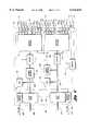
- FIG. 1is a block diagram of a computer system having a DASD controller with a traditional parallel bus architecture
- FIG. 2is a block diagram of a computer system having a DASD controller according to the present invention
- FIG. 3is a schematic diagram of a set of driver and receiver pairs implementing a multichannel serial link according to the present invention
- FIG. 4is a schematic diagram of an illustrative cache architecture that may use the present invention showing a portion of the data connections;
- FIG. 5is a schematic diagram of an exemplary serial hub for simplex operation according to the present invention.
- FIG. 6is a schematic diagram of an exemplary serial hub for duplex operation according to the present invention.
- FIG. 7is a schematic diagram of an illustrative control architecture according to the present invention.
- FIG. 8is a schematic diagram of a pair of memory cards including simplex hubs that may be used in the architecture shown in FIG. 7;
- FIG. 9is a schematic diagram of a pair of memory cards including duplex hubs that may be used in the architecture shown in FIG. 7;
- FIG. 10is a conceptualized timing diagram illustrating a control sequence for a simplex embodiment of the present invention.
- FIG. 11is a conceptualized timing diagram illustrating a control sequence for a duplex embodiment of the present invention.
- FIG. 12is a block diagram of tasks in adapter control logic according to the present invention.
- Parallel bus computer system 20includes parallel bus DASD controller 22 and mainframe elements such as processors 24 and disk arrays 25.
- Processor 24may be connected to parallel bus DASD controller 22 through processor bus 26 such as SCSI (Small Computer System Interface), ESCON (Enterprise System Connection), HIPPI (High Performance Parallel Interface), Fiber Channel, or FIPS (Federal Information Processing Standard).
- Disk array 25may be connected to parallel bus DASD controller 22 through disk array bus 27 such as SCSI or Fiber Channel.
- disk array bus 27such as SCSI or Fiber Channel.
- Parallel bus DASD controller 22contains parallel cache 28.
- a cacheis a large memory system accessible by processor 24 or disk array 25.
- Parallel adapter 30is operative to interface with processor 24 or disk array 25 through processor bus 26 or disk array bus 27 respectively and thereby access cache 28 using parallel bus 32.
- Serial link computer system 40includes the same processors 24, disk arrays 25, processor buses 26 and disk array buses 27 as in parallel computer system 20.
- serial link DASD controller 42is substituted for parallel DASD controller 22.
- three processors, three disk arrays, and six adaptersare shown, any number of processors and disk arrays together with their associated adapters are possible in computer system 40.
- DASD controller 42contains serial cache 44.
- Serial adapter 46provides the interface between processor 24 or disk array 25 and cache 44, connected through processor bus 26 or disk array bus 27 respectively and adapter 46. A performance increase will occur by replacing parallel bus 32 with bidirectional multichannel serial link 48 between each adapter 46 and cache 44.
- Each bidirectional multichannel serial link 48includes two unidirectional multichannel serial links, each unidirectional link providing communication in one direction.
- Group serial transmitter 60sends and group serial receiver 62 (RX) receives serial signals over a set of three or more serial channels, shown generally by 64.
- Set of serial channels 64 connecting group serial transmitter 60 and group serial receiver 62defines a point-to-point unidirectional multichannel serial path.
- Group serial transmitter 60accepts parallel data in input register 66 clocked by input parallel clock 68. Group serial transmitter 60 also accepts control input on control in bus 70. Control input may include, but is not limited to, indications for error, read frame, write frame, diagnostic frame, start of frame, and end of frame.
- Encoder 72receives control input from control in bus 70 and data from input register 66. Encoder 72 develops a parallel code corresponding to either the control input on control in bus 70 or the data value in input register 66 depending on the control input on control in bus 70.
- Parallel-to-serial register 74accepts a portion of the parallel code from encoder 72 and shifts out a serial sequence bit stream clocked by serial clock 76.
- Serial clock 76is produced by multiplying the frequency of input parallel clock 68 by a value equal to the number of bits in parallel-to-serial register 74.
- Serial clock driver 78outputs a signal corresponding to serial clock 76 onto serial clock channel 80.
- Serial data channel 82transmits a signal corresponding to the serial sequence bit stream produced by parallel-to-serial register 74.
- serial data drivers 78 and serial clock driver 84are implemented with a serial flat panel display driver having a differential output such as the SII140 manufactured by Silicon Image, Inc.
- serial flat panel display driverhaving a differential output such as the SII140 manufactured by Silicon Image, Inc.
- the non-standard use of serial flat panel display driversallows construction of a high reliability communication link. This link has an inherently low cost due to the volume leverage of the flat panel display industry. Furthermore, continued developments in flat panel technology will produce increasing serial transfer rates and increasing functionality at decreasing piece prices.
- encoder 72is operative to produce a DC balanced signal.
- encoder 72accepts a 24-bit input word and develops a 30-bit code.
- the 30-bit codeis divided into three 10-bit codes, each of which is DC balanced within one bit.
- the one-bit out of-balanceis compensated for by inserting idle clockings between frames.
- Each 10-bit codeis clocked into a corresponding parallel-to-serial register 74.
- group serial receiver 62accepts serial channels 64 and outputs control on control out bus 90 corresponding to the control signal input on control in bus 70, output parallel clock 92 corresponding to input parallel clock 68, and output parallel data 94 clocked by output parallel clock 92 corresponding to the data received by input register 66.
- Serial clock receiver 96accepts serial clock channel 80 and outputs serial clock 98. Each serial channel 82 carrying a serial sequence bit stream is received by a serial data receiver 100. Serial data receiver 100 outputs a signal to serial-to-parallel register 102 clocked by serial clock 98. Each serial to-parallel register 102 delivers a parallel word to decoder 104. Decoder 104 produces a control signal on control out bus 90 or a parallel data word depending on the value received by decoder 104. Serial clock 98 is divided by a factor equal to the number of bits in serial-to-parallel register 102 to produce output parallel clock 92. Data output from decoder 104 is clocked into output register 106 by output parallel clock 92. The output of output register 106 is output parallel data 94.
- serial data receivers 100 and serial clock receiver 96are implemented with a serial flat panel display receiver having a differential input and matching serial data drivers 78 and serial clock driver 84, such as the SII141 manufactured by Silicon Image, Inc.
- Decoder 104converts the balance coded input from serial-to-parallel registers 102 into an uncoded value. To match the encoding scheme used in group serial transmitter 60, three 10-bit registers 102 are used for serial-to-parallel conversion and the resulting 30-bit encoded value is decoded by decoder 104.
- FIG. 4a schematic diagram of an illustrative cache architecture according to the present invention is shown. As will be described below, only a portion of the data connections have been included.
- DASD controller 42includes sixteen adapters, one of which is indicated by 46.
- Cache 44is divided into at least one memory card. The example shown has four cards indicated as Cache 0 130, Cache 0' 132, Cache 1 134, and Cache 1' 136. Memory cards are grouped in pairs, one card being a master and one a slave. Master cards 130,134 are designated by cache numbers without primes and slave cards 132,136 by cache numbers with primes.
- each cardis divided into memory banks, one of which is indicated by 138.
- Each memory bank 138can service one memory request at a time.
- each memory cardhas five memory banks indicated by M0, Ml, M2, M3, and M4.
- all master cards 130,134are directly connected to each adapter 46 in the top half of arbiters indicated as A0 through A3 and B0 through B3.
- All slave cards 132,136are directly connected to each adapter 46 in the bottom half of adapters 46 indicated as A0' through A3' and B0' through B3'.
- FIG. 4the data write links from adapters 46 to memory cards 130,134 for the top half and the data read links from memory cards 132,136 to adapters 46 for the bottom half are shown.
- the adapters 46are divided into two sets with every adapter 46 in a first set connected to each master memory card 130,134 and each adapter 46 in a second set connected to each slave memory card 132,136.
- Each link 48is shown as a pair of unidirectional links comprising group serial transmitter 60 connected to group serial receiver 62 through serial channels 64. The operation of a unidirectional link is described with regards to FIG. 3 above.
- each master-slave pairis connected by intercard data buses, one of which is indicated by 140.
- intercard data buses 140reduces the number of multichannel serial data links 64 required. Arbitration by the master card and the slave card, discussed with regards to FIGS. 6 through 8 below, determines access to memory banks 138.
- FIG. 5a schematic diagram of an exemplary serial hub for simplex operation according to the present invention is shown.
- At least one simplex hub 160is used on each memory card 130,132,134, 136 in embodiments of the present invention that use simplex hub 160.
- eight adaptersare connected to hub 62, as indicated by the eight incoming unidirectional links 64 and eight outgoing unidirectional links 64.
- Each simplex hub 160can provide access to one memory bank 138, not shown for clarity, during a memory access period.
- Simplex arbiter 162determines which adapter 46 connected to memory card 130,132,134,136 will be selected. Each adapter 46 connected to hub 160 has a request line, the collection of which is indicated by request bus 164. Arbiter 162 indicates which adapter 46 is selected by asserting the corresponding grant line, the collection of which is indicated by grant bus 166. Adapter 46 is also connected to bank bus 168. Once granted access, adapter 46 indicates to which bank access is requested by placing the bank number on bank bus 168. Control and arbitration is further discussed with regards to FIGS. 7, 8, and 10 below.
- the receive data pathbegins with a set of incoming unidirectional serial data links 64. Each link is connected to a group serial receiver 62, which outputs short parallel data 94 corresponding to a received sequence of serial bits.
- group serial receiver 62The operation of group serial receiver 62 is described with regards to FIG. 3 above.
- the output of each group serial receiver 62is input into receive section 170.
- Receive section 170operates as a multiplexer, using selected adapter signal 171 from arbiter 162 to select which group serial receiver 62 output to forward to assembler 172.
- Receive section 170must switch between different group serial receivers 62, each driven by a clock in corresponding adapter 46, without allowing glitching.
- a design for glitchless receivingis described in U.S. Patent application (attorney docket 97-062-DSK) entitled "System and Method for Multiplexing Serial Links" by W. Burns and M. Lucas, which is hereby incorporated by reference.
- Assembler 172accepts three short parallel data words and constructs a wide parallel word.
- short parallel data 94is 24 bits and the wide parallel words are 72 bits.
- Format decoder 174accepts the output of assembler 172 as well as frame commands from the control out bus 90 of each group serial receiver 62. Format decoder 174 decodes memory address and mode information contained in the frame commands. Format decoder 174 also identifies the field type, stores the current mode, and outputs control signals. Format encoder outputs data onto internal data bus 176.
- Cyclic redundancy code (CRC) module 178checks the accuracy of incoming data using bits included in the wide data word.
- Error detection and correction (EDAC) module 180introduces bits to detect and correct errors introduced while data is stored in memory bank 138.
- Each memory bank 138 served by hub 160is connected to hub 160 through data bus 182.
- the address of the current write location in memoryis held in address buffer 184 and sent to memory bank 138 on address bus 186.
- Address bufferis loaded by format decoder 174.
- the transmit data pathis substantially the reverse of the receive data path.
- Address buffer 184puts out the location to be read on address bus 186.
- the datais read from memory bank 138 onto bus 182 and into EDAC module 180.
- EDAC module 180checks and corrects errors introduced by data storage and outputs the corrected data to internal data bus 176.
- CRC module 178adds bits for detecting and correcting errors in transmission.
- Format encoder 188generates stage frame commands for delivery to each group serial transmitter 60.
- Disassembler 190breaks wide parallel words into short parallel words.
- Transmit section 192serves as a demultiplexer, selecting the appropriate group serial transmitter 60 based on selected adapter signal 171. Data is sent from group serial transmitter 60 on unidirectional multichannel serial link 64.
- duplex hub 200is included on each memory card 130,132, 134,136 in embodiments of the present invention using duplex hub 200.
- the operation of duplex hub 200is similar to the operation of simplex hub 160 described with regards to FIG. 5 above except that duplex hub 200 is capable of simultaneous memory read and write.
- duplex hub 200In order to accomplish simultaneous memory read and write, duplex hub 200 must have two copies of all memory access components.
- internal data bus 176becomes internal write bus 202 and internal read bus 204.
- Two copies of CRC module 178, EDAC 180, and address buffer 184are needed.
- Two buses to memory banks 138are required.
- Write bus 206sends data to memory at the location specified by write address 208.
- Read bus 210receives data from memory at the location specified by read address 212.
- Duplex arbiter 214must determine if either or both of memory read and write will occur. Control and arbitration is described with regards to FIGS. 7, 9, 10, and 11 below.
- FIG. 7a schematic diagram of an illustrative control architecture according to the present invention is shown.
- sixteen adaptersone of which is indicated by 46, can access four memory cards 130,132,134,136.
- adaptersare divided into "A side" and "B side". In FIG. 7, only the A side adapters 46 are shown connected. Each side is further divided into a top half and a bottom half, the adapters in the top half having number designations such as 0, 1, 2, . . . and the adapters in the bottom half having number designations with primes such as 0', 1', 2', . . .
- One of ordinary skill in the artwill recognize that the choice of top and bottom and of numerical designation is arbitrary.
- Memory cardsare also split into two groups, master memory cards 130,134 and slave memory cards 132,136, with each master having a corresponding slave. If an odd number of memory cards are used, there will be one more master than slave memory cards.
- each adapter 46 in the top halfrequests access directly to all master memory cards 130,134, and each adapter 46 in the bottom half requests access directly to all slave memory cards 132,136.
- a request lineruns from each adapter 46 to all of the corresponding memory cards in the appropriate half.
- adapter A0has a request line to Cache 0 130, labeled Ra -- c0(0), which is part of request bus 164 and a request line to Cache 1 134, labeled Ra -- c1(0).
- a grant lineruns to each adapter 46 from all of the corresponding memory cards in the appropriate half.
- adapter A0has a grant line from Cache 0 130, labeled Ga -- c0(0), which is part of grant bus 166 and a grant line from Cache 1 134, labeled Ga -- c1(0).
- a parallel bank busconnects adapter 46 in each half of each side with the corresponding memory card 130,132,134,136.
- adapter A0is connected by bank bus 168, labeled Ba -- c0(4:0), to Cache 0 130. All but one of the bank bus lines is used to send the address of the requested bank from adapter 46 to a corresponding memory card.
- ten memory banks 138 in each pair of memory cards 130,132require four lines.
- the last line in bank bus 168is used by adapter 46 to signal that the bank address is valid.
- a separate bank busis shown for each side of adapters 46 for redundancy. Timing diagrams describing the use of request, grant, and bank control lines is described with regards to FIGS. 8 and 11 below.
- each memory cardhas five memory banks 138 and one hub 160 connected to eight adapters 46.
- Master memory card 130shares data with slave memory card 132 through two intercard data buses 140.
- Each bus 140corresponds to an intracard data path.
- Path A 240connects hub 160 in Cache 0 130 to each of the five memory banks 138 in Cache 0 130 and, through a first intercard bus 140, to each of the five memory banks 138 in Cache 0' 132.
- Path B 242connects hub 160 in Cache 0' 132 to each of the five memory banks 138 in Cache 0' 132 and, through a second intercard bus 140, to each of the five memory banks 138 in Cache 0 130.
- Transceiver pairsone pair of which is labeled 244, provide a buffer between internal paths 240,242 and memory banks 138 and between internal paths 240,242 and intercard buses 140.
- paths 240,242, intercard buses 140, and memory banks 138all have the same data width as the wide parallel word developed by assembler 172 described with regards to FIGS. 5 and 6 above. In the exemplary embodiment, this data width is 72 bits.
- Each hub 160,200 in a master memory card such as Cache 0 130has master arbiter 246.
- Master arbiter 246may be arbiter 162 for simplex hub 160 or arbiter 214 for duplex hub 200.
- Each hub 160,200 in a slave memory card such as Cache 0' 132has slave arbiter 248.
- Slave arbiter 248may be arbiter 162 for simplex hub 160 or arbiter 214 for duplex hub 200.
- Each arbiter 246,248is connected to adapters 46 in the appropriate half by request bus 164, grant bus 166, and bank bus 168, as described with regards to FIG. 7 above. In FIG.
- request bus 164is split into two groups of connections, the A Side connections are labeled Ra(3:0) and the B Side connections are labeled Rb(3:0).
- grant bus 166is labeled Ga(3:0) for the A Side and Gb(3:0) for the B Side.
- Bank bus 168has been split into two buses for redundancy. Each of these buses has been further split to show the bank address lines and bank valid line separately.
- the A side address busis labeled Ba(3:0)
- the B side address busis labeled Bb(3:0)
- the A Side bank valid lineis labeled Bva
- the B Side bank valid lineis labeled Bvb.
- Intercard bank bus 250provides master arbiter 246 with the bank address from a selected adapter 46 in the lower half of adapters. The purpose of intercard bank bus 250 will be described with regards to FIG. 10 below.
- Intercard control bus 252carries control signals between master arbiter 246 and slave arbiter 248 for synchronization and acknowledgement.
- each master memory card 130 and slave memory card 132 paircan provide access to two memory banks 138 simultaneously. Further, due to intercard data buses 140 and dual paths 240,242, both accesses may be on the same memory card 130,132. The decision as to which adapters 46 will be granted access comes from arbiters 246,248.
- duplex hub 200Operation of duplex hub 200 is described with regards to FIG. 6 above.
- the operation of memory cards 130,132 with duplex hubs 200is similar to the operation of memory cards with simplex hubs 160 described with regards to FIG. 8 above except that each hub can make two simultaneous memory accesses, a read and a write.
- each memory card 130,132has one hub 200.
- a pathconnects each hub 200 in the card pair 130,132 with memory banks 138.
- Path A 240connects hub 200 in master memory card 130 with memory banks 138 in both master memory card 130 and slave memory card 132.
- Path B 242connects hub 200 in slave memory card 132 with memory banks 138 in both master memory card 130 and slave memory card 132.
- each path 240,242includes two data buses, write bus 208 and read bus 210.
- Multiplexer 254 before each transceiver pair 244selects between write bus 208 and read bus 210.
- Intercard data bus 140is doubled in width, with master-to-slave bus 256 providing for parallel data flow in one direction and slave-to-master bus 258 providing for parallel data flow in the other direction.
- Parallel transmitter 260 and parallel receiver 262provide buffers for buses 256,258.
- Each master memory cardsuch as Cache 0 130, has master arbiter 264.
- Each slave memory cardsuch as Cache 0' 132, has slave arbiter 266.
- Each arbiter 264,266is connected to adapters 46 in the appropriate set of adapters 46 by request bus 164, grant bus 166, and bank bus 168, as described with regards to FIGS. 7 and 8 above. However, in order to permit simultaneous read and write for each hub, modifications are required.
- bank buses 168are increased in size such that two bank addresses may be sent simultaneously.
- bank buses 168become Ba(7:0) and Bb(7:0) in FIG. 9.
- bank buses 168are the same width and bank addresses are transmitted sequentially. For example, the memory read bank address is transmitted then the memory write bank address is transmitted.
- Intercard bank bus 250provides master arbiter 246 with the bank address from a selected adapter 46 in the lower half of adapters. The purpose of intercard bank bus 250 will be described with regards to FIG. 10 below.
- Intercard control bus 268carries control signals between master arbiter 264 and slave arbiter 266 for synchronization and acknowledgement.
- each master memory card 130 and slave memory card 132 paircan provide access to four memory banks 138 simultaneously. Further, due to intercard data buses 256,258 and dual paths 240,242, all four accesses may be on the same memory card 130,132. The decision as to which adapters 46 will be granted access comes from arbiters 264,266. Arbitration is discussed with regards to FIGS. 10 and 11 below.
- FIG. 10a conceptualized timing diagram illustrating a control sequence for the architecture of FIG. 7 is shown.
- the timing diagramshows one request sequence for Cache 0 130 and Cache 0' 132.
- the sequencebegins with each adapter 46 desiring access asserting its corresponding request line of request bus 164.
- Request bus Ra -- c0(3:0)indicates adapters A0 and A2 desire access to Cache 0 130, as shown by request signals 270.
- Request bus Rb -- c0indicates adapters B0, B2 and B3 desire access to Cache 0 130, as shown by request signals 271.
- Request bus Ra -- c0'indicates adapter A2' desires access to Cache 0' 132, as shown by request signals 272.
- Request bus Rb -- c0'indicates adapters B0' and B3' desire access to Cache 0' 132, as shown by request signal 273.
- Arbiters 246,248each select adapters 46 to which access may be granted.
- one adapter 46may be selected for each simplex hub 160 or duplex hub 200.
- One scheme for arbitrationis a round robin selection that toggles priority between sides for each request sequence and takes adapters on each side in numerical order. For example, if all adapters desired access, the sequence of grants might be A0, B0, A1, B1, A2, . . .
- Other arbitration algorithmsare possible, including granting priority to least recently used, least frequently used, most recently used, and random selection. Most recently used is attractive in that, if memory banks 138 are comprised of dynamic RAM (DRAM) arranged in rows, significant speedup can be achieved by accessing a row left open from the previous access.
- DRAMdynamic RAM
- round robin priorityis used.
- each arbiter 246,248asserts the appropriate grant line of grant bus 166.
- adapters A0 and B3'have been selected as indicated by grant bus signal sets Ga -- c0(3:0) 274, Gb -- c0(3:0) 275, Ga -- c0' (3:0) 276, and Gb -- c0' (3:0) 277.
- Each selected adapter 46outputs the address of the desired memory bank 138.
- adapter A0requests access to bank M4 of Cache 0 130 and adapter B3' requests access to bank M3 of Cache 0 130, as shown in bank signals 278 and 281. Since no adapter in the top half of Side B or the bottom half of Side A are selected, the values for bank signals 279 and 280 are irrelevant.
- Bank valid signal Bva -- c0 282is asserted by adapter A0 and is received by master arbiter 246 to indicate that bank signal 278 is valid.
- Adapter B3'asserts signal Bvb -- c0' 283 for slave arbiter 248.
- bank arbitrationbegins. Since two or more selected adapters may request the same bank on the same memory card 130,132, bank arbitration is required. In the exemplary embodiment described in FIG. 10, if an arbiter from the lower half was selected, slave arbiter 248 forwards the bank number to master arbiter 246 on intercard bank bus 250. If an arbiter from the upper half was selected, master arbiter 246 then compares the bank address received from the selected adapter 46 with the bank address forwarded from slave arbiter 248. If the two requested banks are the same, master arbiter 246 selects which adapter 46 will gain access to memory.
- each selected adapter 46is granted access.
- a bank arbitration method for one simplex hub 160 per memory card 130,132is to always grant access to adapter 46 from a particular half such as, for example, always granting access to adapter 46 connected to master memory card 130.
- Another bank arbitration methodis to alternate between top and bottom half adapters 46. In a preferred embodiment, fairness is achieved by alternating access between A-side and B-side adapters 46.
- arbiters 246,248store the bank addresses of ungranted requests for use in subsequent arbitration.
- the stored bank addressesare compared with bank addresses received from selected adapters 46 to maximize utilization of memory banks 138 by minimizing bank conflicts.
- arbiters 246,248indicate to which adapters 46 access has been granted using grant bus 166.
- arbiters 246,248indicate to which adapters 46 access has been granted using grant bus 166.
- arbiters 246,248indicate to which adapters 46 access has been granted using grant bus 166.
- grant bus signalsets Ga -- c0(3:0) 284, Gb -- c0(3:0) 285, Ga -- c0' (3:0) 286, and Gb -- c0' (3:0) 287.
- Data transfermay then begin, as indicated by new valid data signal 288.
- data transfer and arbitrationare overlapped, as indicated by previous valid data signal 289.
- the timing diagram in FIG. 10may be modified for duplex hubs 200 connected to adapters 46 through wide bank buses 168. Both the transmit and receive bank address are provided in bank signal 278,281. After bank arbitration, two sequential grant signals 284,287 are then sent to each selected adapter 46, one indicating if the transmit bank address is granted and one indicating if the receive bank address is granted.
- bank bus 168has sufficient width to transmit one bank address at a time.
- Adapter 46requests access to memory banks 138 by first sending the bank address for read then sending the bank address for write. Signals for adapter request 270, 271,272,273 and for adapter select 274,275,276,277 are described with regards to FIG. 10 above.
- adapter 46places the bank address desired for a write operation on bank bus 168.
- adapter A0requests read access to bank M4 of Cache 0 130 in bank signal 290 and adapter B3' requests read access to bank M3 of Cache 0 130 in bank signal 294.
- the values of bank signals 292,293 from adapters not selectedare not relevant.
- Bank valid signals 295,296are asserted to indicate bank addresses are valid.
- Grant signals 297,298,299,300indicate that both read bank requests are granted by corresponding arbiters 264,266.
- Selected adapters 46now send requests for write access on bank buses 242.
- Adapter A0requests write access to bank M8 in Cache 0' 132 in bank signal 301 and adapter B3' requests write access to bank M4 in Cache 0 130 in bank signal 304.
- bank signals 302,303 on bank buses 168 to adapters 46 not selectedare irrelevant.
- Bank valid signals 295,296are again asserted to indicate valid bank address.
- Grant signals 305,306,307,308indicate that adapter A0 is granted write access to bank M0 of cache C0' 132. However, adapter B3' is not granted access to bank M4 of cache C0 130 since this would conflict with the read access granted to A0. Three simultaneous data transfers may now proceed, as indicated by data valid 288. As in the simplex case, arbitration may be overlapped with data transfer, as indicated by valid data 289 resulting from the previous arbitration.
- the illustrative duplex bank granting technique described abovefavors memory reads by granting access to read bank requests first.
- write bank requestsmay be transmitted and arbitered first.
- Another possibilityis to send both read and write bank addresses prior to any arbitration and then grant access to memory banks 138.
- bank bus 168is wide enough to transmit both a read bank address and a write bank address simultaneously.
- bank address signals 290, 294, 301, and 304are transmitted concurrently. This reduces the hardware required in arbiters 246,248.
- FIGS. 10 and 11are conceptualized.
- the signalsare not drawn to indicate actual lengths of time or time overlaps.
- adapters 46are not synchronized to each other and, therefore, signals from adapters 46 may not change simultaneously as shown.
- Control task 320accepts master orders and decomposes the master orders into read and write tasks, which are placed in read queue 322 and write queue 324 respectively.
- Read task 326 and write task 328each take jobs from their respective queues, control data transfer, and report status.
- Master orders 330are received by master order task 332 in control task 320.
- Master order task 332is responsible for decomposing master order 330 into read orders and write orders, determining which orders may be run in parallel, and controlling the functioning of other tasks.
- Master order 330is divided into sections, each of which contains read and write operations that may be carried out in parallel. Once each section is completed, the operations in the next section may be carried out in parallel.
- Master order task 332places read and write orders into first-in first-out order queue 334. Orders are read from order queue 334 by manager task 336, which manages first-in first-out read queue 322 and first-in first-out write queue 324.
- Read task 326is initiated to handle a read order.
- Write task 328is initiated to handle a write order. Both tasks transition through a sequence of phases including Setup, Initiate, Wait, Complete, and, if necessary, Error Recovery. Setup and Initiate take care of internal and external initialization, including partitioning the read or write order into blocks of a size handled by adapter 46 and cache 48 hardware. These blocks are then received as read data 338 or write data 340. Wait is entered while each block is received or transmitted. If all blocks are handled successfully, a Complete state is entered. If an error occurred, Error Recovery state is entered.
- Read task 326provides read status 342 to master order task 332.
- Write task 328provides write status 344 to master order task 332.
- the status 342,344indicates the success or failure of read and write orders.
- Master order task 332must be capable of receiving status 342,344 in any order, since read and write orders may be processed asynchronously and nonsequentially. Master order task 332 reports master order status 346.
- multiple read tasks 326 and write tasks 328may exist concurrently, allowing adapter 46 to proceed with simultaneous staging and destaging if access to a desired memory bank 138 is blocked.
- write task 328is capable of transmitting the same information to multiple locations to facilitate data mirroring for use in, for example, RAID implementations.
Landscapes
- Engineering & Computer Science (AREA)
- Theoretical Computer Science (AREA)
- Physics & Mathematics (AREA)
- General Engineering & Computer Science (AREA)
- General Physics & Mathematics (AREA)
- Memory System Of A Hierarchy Structure (AREA)
Abstract
Description
Claims (26)
Priority Applications (1)
| Application Number | Priority Date | Filing Date | Title |
|---|---|---|---|
| US09/093,140US6134624A (en) | 1998-06-08 | 1998-06-08 | High bandwidth cache system |
Applications Claiming Priority (1)
| Application Number | Priority Date | Filing Date | Title |
|---|---|---|---|
| US09/093,140US6134624A (en) | 1998-06-08 | 1998-06-08 | High bandwidth cache system |
Publications (1)
| Publication Number | Publication Date |
|---|---|
| US6134624Atrue US6134624A (en) | 2000-10-17 |
Family
ID=22237419
Family Applications (1)
| Application Number | Title | Priority Date | Filing Date |
|---|---|---|---|
| US09/093,140Expired - LifetimeUS6134624A (en) | 1998-06-08 | 1998-06-08 | High bandwidth cache system |
Country Status (1)
| Country | Link |
|---|---|
| US (1) | US6134624A (en) |
Cited By (64)
| Publication number | Priority date | Publication date | Assignee | Title |
|---|---|---|---|---|
| US6314482B1 (en)* | 1999-03-19 | 2001-11-06 | International Business Machines Corporation | Method and system for indexing adapters within a data processing system |
| US6389554B1 (en)* | 1997-12-17 | 2002-05-14 | Electronics And Telecommunications Research Institute | Concurrent write duplex device |
| GB2374697A (en)* | 2000-06-29 | 2002-10-23 | Emc Corp | Data storage system having point-to-point configuration |
| US20020194408A1 (en)* | 2001-06-14 | 2002-12-19 | International Business Machines Corporation | Method and system for system performance optimization via heuristically optimized buses |
| US20030101312A1 (en)* | 2001-11-26 | 2003-05-29 | Doan Trung T. | Machine state storage apparatus and method |
| US6581112B1 (en) | 2000-03-31 | 2003-06-17 | Emc Corporation | Direct memory access (DMA) receiver |
| US6584513B1 (en) | 2000-03-31 | 2003-06-24 | Emc Corporation | Direct memory access (DMA) transmitter |
| US6601134B1 (en)* | 1998-04-27 | 2003-07-29 | Hitachi, Ltd. | Multi-processor type storage control apparatus for performing access control through selector |
| US6612492B1 (en)* | 2002-06-06 | 2003-09-02 | Chant Sincere Co., Ltd. | Four-in-one memory card insertion port |
| US6651130B1 (en) | 2000-04-28 | 2003-11-18 | Emc Corporation | Data storage system having separate data transfer section and message network with bus arbitration |
| US6779071B1 (en) | 2000-04-28 | 2004-08-17 | Emc Corporation | Data storage system having separate data transfer section and message network with status register |
| US20040260872A1 (en)* | 2003-06-20 | 2004-12-23 | Fujitsu Siemens Computers Gmbh | Mass memory device and method for operating a mass memory device |
| US20050097276A1 (en)* | 2001-09-28 | 2005-05-05 | Lu Shih-Lien L. | Hiding refresh of memory and refresh-hidden memory |
| US20050132159A1 (en)* | 2002-08-16 | 2005-06-16 | Jeddeloh Joseph M. | Memory hub bypass circuit and method |
| US20050146943A1 (en)* | 2003-08-28 | 2005-07-07 | Jeddeloh Joseph M. | Memory module and method having on-board data search capabilities and processor-based system using such memory modules |
| US20050177677A1 (en)* | 2004-02-05 | 2005-08-11 | Jeddeloh Joseph M. | Arbitration system having a packet memory and method for memory responses in a hub-based memory system |
| US6957285B2 (en) | 1998-12-30 | 2005-10-18 | Emc Corporation | Data storage system |
| US6980042B2 (en) | 2004-04-05 | 2005-12-27 | Micron Technology, Inc. | Delay line synchronizer apparatus and method |
| US6993621B1 (en) | 2000-03-31 | 2006-01-31 | Emc Corporation | Data storage system having separate data transfer section and message network with plural directors on a common printed circuit board and redundant switching networks |
| US7003601B1 (en) | 2000-03-31 | 2006-02-21 | Emc Corporation | Data storage system having separate data transfer section and message network with plural directions on a common printed circuit board |
| US7007194B1 (en) | 2000-06-29 | 2006-02-28 | Emc Corporation | Data storage system having point-to-point configuration |
| US7010575B1 (en) | 2000-03-31 | 2006-03-07 | Emc Corporation | Data storage system having separate data transfer section and message network having bus arbitration |
| US7073020B1 (en) | 1999-01-04 | 2006-07-04 | Emc Corporation | Method for message transfer in computer storage system |
| US7107415B2 (en) | 2003-06-20 | 2006-09-12 | Micron Technology, Inc. | Posted write buffers and methods of posting write requests in memory modules |
| US7106611B2 (en) | 2002-09-09 | 2006-09-12 | Micron Technology, Inc. | Wavelength division multiplexed memory module, memory system and method |
| US7117275B1 (en) | 1999-01-04 | 2006-10-03 | Emc Corporation | Data storage system having separate data transfer section and message network |
| US7117316B2 (en)* | 2002-08-05 | 2006-10-03 | Micron Technology, Inc. | Memory hub and access method having internal row caching |
| US7120743B2 (en) | 2003-10-20 | 2006-10-10 | Micron Technology, Inc. | Arbitration system and method for memory responses in a hub-based memory system |
| US7120723B2 (en) | 2004-03-25 | 2006-10-10 | Micron Technology, Inc. | System and method for memory hub-based expansion bus |
| US7120727B2 (en) | 2003-06-19 | 2006-10-10 | Micron Technology, Inc. | Reconfigurable memory module and method |
| US7133972B2 (en) | 2002-06-07 | 2006-11-07 | Micron Technology, Inc. | Memory hub with internal cache and/or memory access prediction |
| US7133991B2 (en) | 2003-08-20 | 2006-11-07 | Micron Technology, Inc. | Method and system for capturing and bypassing memory transactions in a hub-based memory system |
| US7136958B2 (en) | 2003-08-28 | 2006-11-14 | Micron Technology, Inc. | Multiple processor system and method including multiple memory hub modules |
| US7162567B2 (en) | 2004-05-14 | 2007-01-09 | Micron Technology, Inc. | Memory hub and method for memory sequencing |
| US7181584B2 (en) | 2004-02-05 | 2007-02-20 | Micron Technology, Inc. | Dynamic command and/or address mirroring system and method for memory modules |
| US7180522B2 (en) | 2000-06-23 | 2007-02-20 | Micron Technology, Inc. | Apparatus and method for distributed memory control in a graphics processing system |
| US7188219B2 (en) | 2004-01-30 | 2007-03-06 | Micron Technology, Inc. | Buffer control system and method for a memory system having outstanding read and write request buffers |
| US7194593B2 (en) | 2003-09-18 | 2007-03-20 | Micron Technology, Inc. | Memory hub with integrated non-volatile memory |
| US20070067540A1 (en)* | 2003-08-08 | 2007-03-22 | Hewlett-Packard Development Company, L.P. | Method and apparatus for sending data |
| US7200024B2 (en) | 2002-08-02 | 2007-04-03 | Micron Technology, Inc. | System and method for optically interconnecting memory devices |
| US7210059B2 (en) | 2003-08-19 | 2007-04-24 | Micron Technology, Inc. | System and method for on-board diagnostics of memory modules |
| US7213082B2 (en) | 2004-03-29 | 2007-05-01 | Micron Technology, Inc. | Memory hub and method for providing memory sequencing hints |
| US7222197B2 (en) | 2003-07-22 | 2007-05-22 | Micron Technology, Inc. | Apparatus and method for direct memory access in a hub-based memory system |
| US7234070B2 (en) | 2003-10-27 | 2007-06-19 | Micron Technology, Inc. | System and method for using a learning sequence to establish communications on a high-speed nonsynchronous interface in the absence of clock forwarding |
| US7242213B2 (en) | 2003-06-11 | 2007-07-10 | Micron Technology, Inc. | Memory module and method having improved signal routing topology |
| US7249236B2 (en) | 2002-08-29 | 2007-07-24 | Micron Technology, Inc. | Method and system for controlling memory accesses to memory modules having a memory hub architecture |
| US7254331B2 (en) | 2002-08-09 | 2007-08-07 | Micron Technology, Inc. | System and method for multiple bit optical data transmission in memory systems |
| US7257683B2 (en) | 2004-03-24 | 2007-08-14 | Micron Technology, Inc. | Memory arbitration system and method having an arbitration packet protocol |
| US7260685B2 (en) | 2003-06-20 | 2007-08-21 | Micron Technology, Inc. | Memory hub and access method having internal prefetch buffers |
| US7310752B2 (en) | 2003-09-12 | 2007-12-18 | Micron Technology, Inc. | System and method for on-board timing margin testing of memory modules |
| US7310748B2 (en) | 2004-06-04 | 2007-12-18 | Micron Technology, Inc. | Memory hub tester interface and method for use thereof |
| US7330992B2 (en) | 2003-12-29 | 2008-02-12 | Micron Technology, Inc. | System and method for read synchronization of memory modules |
| US7363419B2 (en) | 2004-05-28 | 2008-04-22 | Micron Technology, Inc. | Method and system for terminating write commands in a hub-based memory system |
| US7392331B2 (en) | 2004-08-31 | 2008-06-24 | Micron Technology, Inc. | System and method for transmitting data packets in a computer system having a memory hub architecture |
| US7428644B2 (en) | 2003-06-20 | 2008-09-23 | Micron Technology, Inc. | System and method for selective memory module power management |
| US7447240B2 (en) | 2004-03-29 | 2008-11-04 | Micron Technology, Inc. | Method and system for synchronizing communications links in a hub-based memory system |
| US7519788B2 (en) | 2004-06-04 | 2009-04-14 | Micron Technology, Inc. | System and method for an asynchronous data buffer having buffer write and read pointers |
| US7590797B2 (en) | 2004-04-08 | 2009-09-15 | Micron Technology, Inc. | System and method for optimizing interconnections of components in a multichip memory module |
| US7788451B2 (en) | 2004-02-05 | 2010-08-31 | Micron Technology, Inc. | Apparatus and method for data bypass for a bi-directional data bus in a hub-based memory sub-system |
| US20100235716A1 (en)* | 2006-06-30 | 2010-09-16 | Guillermo Rozas | Dual ported replicated data cache |
| US7805586B2 (en) | 2002-08-29 | 2010-09-28 | Micron Technology, Inc. | System and method for optimizing interconnections of memory devices in a multichip module |
| US8775764B2 (en) | 2004-03-08 | 2014-07-08 | Micron Technology, Inc. | Memory hub architecture having programmable lane widths |
| US20170132137A1 (en)* | 2015-11-09 | 2017-05-11 | International Business Machines Corporation | Implementing hardware accelerator for storage write cache management for reads from storage write cache |
| US10289592B1 (en)* | 2017-11-09 | 2019-05-14 | Funai Electric Co., Ltd. | Location-based address adapter and system |
Citations (2)
| Publication number | Priority date | Publication date | Assignee | Title |
|---|---|---|---|---|
| US4430710A (en)* | 1981-08-24 | 1984-02-07 | Burroughs Corporation | Subsystem controller |
| US4520452A (en)* | 1982-03-16 | 1985-05-28 | Burroughs Corporation | Memory selection in a multiple line adapter organization |
- 1998
- 1998-06-08USUS09/093,140patent/US6134624A/ennot_activeExpired - Lifetime
Patent Citations (2)
| Publication number | Priority date | Publication date | Assignee | Title |
|---|---|---|---|---|
| US4430710A (en)* | 1981-08-24 | 1984-02-07 | Burroughs Corporation | Subsystem controller |
| US4520452A (en)* | 1982-03-16 | 1985-05-28 | Burroughs Corporation | Memory selection in a multiple line adapter organization |
Non-Patent Citations (2)
| Title |
|---|
| "SiI140/SiI141 Datasheet", Silicon Image, Inc. Version 1.0 Dec. 1997, Pub. # DS140/141/001-127-100. |
| SiI140/SiI141 Datasheet , Silicon Image, Inc. Version 1.0 Dec. 1997, Pub. DS140/141/001 127 100.* |
Cited By (186)
| Publication number | Priority date | Publication date | Assignee | Title |
|---|---|---|---|---|
| US6389554B1 (en)* | 1997-12-17 | 2002-05-14 | Electronics And Telecommunications Research Institute | Concurrent write duplex device |
| US6601134B1 (en)* | 1998-04-27 | 2003-07-29 | Hitachi, Ltd. | Multi-processor type storage control apparatus for performing access control through selector |
| US20050283576A1 (en)* | 1998-04-27 | 2005-12-22 | Hitachi, Ltd. | Multi-processor type storage control apparatus for performing access control through selector |
| US6963950B2 (en) | 1998-04-27 | 2005-11-08 | Hitachi, Ltd. | Multi-processor type storage control apparatus for performing access control through selector |
| US7167949B2 (en) | 1998-04-27 | 2007-01-23 | Hitachi, Ltd. | Multi-processor type storage control apparatus for performing access control through selector |
| US20040073750A1 (en)* | 1998-04-27 | 2004-04-15 | Hitachi, Ltd. | Multi-processor type storage control apparatus for performing access control through selector |
| US6957285B2 (en) | 1998-12-30 | 2005-10-18 | Emc Corporation | Data storage system |
| US6988152B2 (en) | 1998-12-30 | 2006-01-17 | Emc Corporation | Data storage system |
| US7117275B1 (en) | 1999-01-04 | 2006-10-03 | Emc Corporation | Data storage system having separate data transfer section and message network |
| US7073020B1 (en) | 1999-01-04 | 2006-07-04 | Emc Corporation | Method for message transfer in computer storage system |
| US6314482B1 (en)* | 1999-03-19 | 2001-11-06 | International Business Machines Corporation | Method and system for indexing adapters within a data processing system |
| US6581112B1 (en) | 2000-03-31 | 2003-06-17 | Emc Corporation | Direct memory access (DMA) receiver |
| US7003601B1 (en) | 2000-03-31 | 2006-02-21 | Emc Corporation | Data storage system having separate data transfer section and message network with plural directions on a common printed circuit board |
| US6993621B1 (en) | 2000-03-31 | 2006-01-31 | Emc Corporation | Data storage system having separate data transfer section and message network with plural directors on a common printed circuit board and redundant switching networks |
| US6584513B1 (en) | 2000-03-31 | 2003-06-24 | Emc Corporation | Direct memory access (DMA) transmitter |
| US7010575B1 (en) | 2000-03-31 | 2006-03-07 | Emc Corporation | Data storage system having separate data transfer section and message network having bus arbitration |
| US6651130B1 (en) | 2000-04-28 | 2003-11-18 | Emc Corporation | Data storage system having separate data transfer section and message network with bus arbitration |
| US6779071B1 (en) | 2000-04-28 | 2004-08-17 | Emc Corporation | Data storage system having separate data transfer section and message network with status register |
| US7180522B2 (en) | 2000-06-23 | 2007-02-20 | Micron Technology, Inc. | Apparatus and method for distributed memory control in a graphics processing system |
| GB2374697A (en)* | 2000-06-29 | 2002-10-23 | Emc Corp | Data storage system having point-to-point configuration |
| US7007194B1 (en) | 2000-06-29 | 2006-02-28 | Emc Corporation | Data storage system having point-to-point configuration |
| US20020194408A1 (en)* | 2001-06-14 | 2002-12-19 | International Business Machines Corporation | Method and system for system performance optimization via heuristically optimized buses |
| US6952746B2 (en)* | 2001-06-14 | 2005-10-04 | International Business Machines Corporation | Method and system for system performance optimization via heuristically optimized buses |
| US20050097276A1 (en)* | 2001-09-28 | 2005-05-05 | Lu Shih-Lien L. | Hiding refresh of memory and refresh-hidden memory |
| US20030101312A1 (en)* | 2001-11-26 | 2003-05-29 | Doan Trung T. | Machine state storage apparatus and method |
| US6612492B1 (en)* | 2002-06-06 | 2003-09-02 | Chant Sincere Co., Ltd. | Four-in-one memory card insertion port |
| US8195918B2 (en) | 2002-06-07 | 2012-06-05 | Round Rock Research, Llc | Memory hub with internal cache and/or memory access prediction |
| US20110219196A1 (en)* | 2002-06-07 | 2011-09-08 | Round Rock Research, Llc | Memory hub with internal cache and/or memory access prediction |
| US7945737B2 (en) | 2002-06-07 | 2011-05-17 | Round Rock Research, Llc | Memory hub with internal cache and/or memory access prediction |
| US7644253B2 (en) | 2002-06-07 | 2010-01-05 | Micron Technology, Inc. | Memory hub with internal cache and/or memory access prediction |
| US7133972B2 (en) | 2002-06-07 | 2006-11-07 | Micron Technology, Inc. | Memory hub with internal cache and/or memory access prediction |
| US8499127B2 (en) | 2002-06-07 | 2013-07-30 | Round Rock Research, Llc | Memory hub with internal cache and/or memory access prediction |
| US7382639B2 (en) | 2002-08-02 | 2008-06-03 | Micron Technology, Inc. | System and method for optically interconnecting memory devices |
| US7289347B2 (en) | 2002-08-02 | 2007-10-30 | Micron Technology, Inc. | System and method for optically interconnecting memory devices |
| US7200024B2 (en) | 2002-08-02 | 2007-04-03 | Micron Technology, Inc. | System and method for optically interconnecting memory devices |
| US7411807B2 (en) | 2002-08-02 | 2008-08-12 | Micron Technology, Inc. | System and method for optically interconnecting memory devices |
| US7117316B2 (en)* | 2002-08-05 | 2006-10-03 | Micron Technology, Inc. | Memory hub and access method having internal row caching |
| US8954687B2 (en) | 2002-08-05 | 2015-02-10 | Micron Technology, Inc. | Memory hub and access method having a sequencer and internal row caching |
| US7489875B2 (en) | 2002-08-09 | 2009-02-10 | Micron Technology, Inc. | System and method for multiple bit optical data transmission in memory systems |
| US7254331B2 (en) | 2002-08-09 | 2007-08-07 | Micron Technology, Inc. | System and method for multiple bit optical data transmission in memory systems |
| US7415567B2 (en) | 2002-08-16 | 2008-08-19 | Micron Technology, Inc. | Memory hub bypass circuit and method |
| US7047351B2 (en) | 2002-08-16 | 2006-05-16 | Micron Technology, Inc. | Memory hub bypass circuit and method |
| US20050132159A1 (en)* | 2002-08-16 | 2005-06-16 | Jeddeloh Joseph M. | Memory hub bypass circuit and method |
| US7149874B2 (en) | 2002-08-16 | 2006-12-12 | Micron Technology, Inc. | Memory hub bypass circuit and method |
| US7908452B2 (en) | 2002-08-29 | 2011-03-15 | Round Rock Research, Llc | Method and system for controlling memory accesses to memory modules having a memory hub architecture |
| US8086815B2 (en) | 2002-08-29 | 2011-12-27 | Round Rock Research, Llc | System for controlling memory accesses to memory modules having a memory hub architecture |
| US7249236B2 (en) | 2002-08-29 | 2007-07-24 | Micron Technology, Inc. | Method and system for controlling memory accesses to memory modules having a memory hub architecture |
| US7716444B2 (en) | 2002-08-29 | 2010-05-11 | Round Rock Research, Llc | Method and system for controlling memory accesses to memory modules having a memory hub architecture |
| US7836252B2 (en) | 2002-08-29 | 2010-11-16 | Micron Technology, Inc. | System and method for optimizing interconnections of memory devices in a multichip module |
| US7805586B2 (en) | 2002-08-29 | 2010-09-28 | Micron Technology, Inc. | System and method for optimizing interconnections of memory devices in a multichip module |
| US8234479B2 (en) | 2002-08-29 | 2012-07-31 | Round Rock Research, Llc | System for controlling memory accesses to memory modules having a memory hub architecture |
| US20110167238A1 (en)* | 2002-08-29 | 2011-07-07 | Round Rock Research, Llc | Method and system for controlling memory accesses to memory modules having a memory hub architecture |
| US8190819B2 (en) | 2002-08-29 | 2012-05-29 | Micron Technology, Inc. | System and method for optimizing interconnections of memory devices in a multichip module |
| US7106611B2 (en) | 2002-09-09 | 2006-09-12 | Micron Technology, Inc. | Wavelength division multiplexed memory module, memory system and method |
| US7282947B2 (en) | 2003-06-11 | 2007-10-16 | Micron Technology, Inc. | Memory module and method having improved signal routing topology |
| US7557601B2 (en) | 2003-06-11 | 2009-07-07 | Micron Technology, Inc. | Memory module and method having improved signal routing topology |
| US7242213B2 (en) | 2003-06-11 | 2007-07-10 | Micron Technology, Inc. | Memory module and method having improved signal routing topology |
| US7245145B2 (en) | 2003-06-11 | 2007-07-17 | Micron Technology, Inc. | Memory module and method having improved signal routing topology |
| US7746095B2 (en) | 2003-06-11 | 2010-06-29 | Round Rock Research, Llc | Memory module and method having improved signal routing topology |
| US20110029746A1 (en)* | 2003-06-19 | 2011-02-03 | Round Rock Research, Llc | Reconfigurable memory module and method |
| US7818712B2 (en) | 2003-06-19 | 2010-10-19 | Round Rock Research, Llc | Reconfigurable memory module and method |
| US7120727B2 (en) | 2003-06-19 | 2006-10-10 | Micron Technology, Inc. | Reconfigurable memory module and method |
| US8732383B2 (en) | 2003-06-19 | 2014-05-20 | Round Rock Research, Llc | Reconfigurable memory module and method |
| US8200884B2 (en) | 2003-06-19 | 2012-06-12 | Round Rock Research, Llc | Reconfigurable memory module and method |
| US7966444B2 (en) | 2003-06-19 | 2011-06-21 | Round Rock Research, Llc | Reconfigurable memory module and method |
| US7107415B2 (en) | 2003-06-20 | 2006-09-12 | Micron Technology, Inc. | Posted write buffers and methods of posting write requests in memory modules |
| US7412566B2 (en) | 2003-06-20 | 2008-08-12 | Micron Technology, Inc. | Memory hub and access method having internal prefetch buffers |
| US7428644B2 (en) | 2003-06-20 | 2008-09-23 | Micron Technology, Inc. | System and method for selective memory module power management |
| EP1489519A3 (en)* | 2003-06-20 | 2007-04-04 | Fujitsu Siemens Computers GmbH | Mass memory and method to operate a mass memory |
| US7260685B2 (en) | 2003-06-20 | 2007-08-21 | Micron Technology, Inc. | Memory hub and access method having internal prefetch buffers |
| US7447842B2 (en) | 2003-06-20 | 2008-11-04 | Fujitsu Siemens Computers Gmbh | Mass memory device and method for operating a mass memory device |
| US20040260872A1 (en)* | 2003-06-20 | 2004-12-23 | Fujitsu Siemens Computers Gmbh | Mass memory device and method for operating a mass memory device |
| US7529896B2 (en) | 2003-06-20 | 2009-05-05 | Micron Technology, Inc. | Memory modules having a memory hub containing a posted write buffer, a memory device interface and a link interface, and method of posting write requests in memory modules |
| US8127081B2 (en) | 2003-06-20 | 2012-02-28 | Round Rock Research, Llc | Memory hub and access method having internal prefetch buffers |
| US7437579B2 (en) | 2003-06-20 | 2008-10-14 | Micron Technology, Inc. | System and method for selective memory module power management |
| US7389364B2 (en) | 2003-07-22 | 2008-06-17 | Micron Technology, Inc. | Apparatus and method for direct memory access in a hub-based memory system |
| US7222197B2 (en) | 2003-07-22 | 2007-05-22 | Micron Technology, Inc. | Apparatus and method for direct memory access in a hub-based memory system |
| US7966430B2 (en) | 2003-07-22 | 2011-06-21 | Round Rock Research, Llc | Apparatus and method for direct memory access in a hub-based memory system |
| US8209445B2 (en) | 2003-07-22 | 2012-06-26 | Round Rock Research, Llc | Apparatus and method for direct memory access in a hub-based memory system |
| US7506085B2 (en)* | 2003-08-08 | 2009-03-17 | Hewlett-Packard Development Company, L.P. | System and method for sending data across a bus cable having in-band and side-band signal conductors |
| US20070067540A1 (en)* | 2003-08-08 | 2007-03-22 | Hewlett-Packard Development Company, L.P. | Method and apparatus for sending data |
| US7278060B2 (en) | 2003-08-19 | 2007-10-02 | Micron Technology, Inc. | System and method for on-board diagnostics of memory modules |
| US7913122B2 (en) | 2003-08-19 | 2011-03-22 | Round Rock Research, Llc | System and method for on-board diagnostics of memory modules |
| US7516363B2 (en) | 2003-08-19 | 2009-04-07 | Micron Technology, Inc. | System and method for on-board diagnostics of memory modules |
| US7210059B2 (en) | 2003-08-19 | 2007-04-24 | Micron Technology, Inc. | System and method for on-board diagnostics of memory modules |
| US7251714B2 (en) | 2003-08-20 | 2007-07-31 | Micron Technology, Inc. | Method and system for capturing and bypassing memory transactions in a hub-based memory system |
| US7133991B2 (en) | 2003-08-20 | 2006-11-07 | Micron Technology, Inc. | Method and system for capturing and bypassing memory transactions in a hub-based memory system |
| US7386649B2 (en) | 2003-08-28 | 2008-06-10 | Micron Technology, Inc. | Multiple processor system and method including multiple memory hub modules |
| US7873775B2 (en) | 2003-08-28 | 2011-01-18 | Round Rock Research, Llc | Multiple processor system and method including multiple memory hub modules |
| US8244952B2 (en) | 2003-08-28 | 2012-08-14 | Round Rock Research, Llc | Multiple processor system and method including multiple memory hub modules |
| US20110113189A1 (en)* | 2003-08-28 | 2011-05-12 | Round Rock Research, Llc | Multiple processor system and method including multiple memory hub modules |
| US7581055B2 (en) | 2003-08-28 | 2009-08-25 | Micron Technology, Inc. | Multiple processor system and method including multiple memory hub modules |
| US7136958B2 (en) | 2003-08-28 | 2006-11-14 | Micron Technology, Inc. | Multiple processor system and method including multiple memory hub modules |
| US9082461B2 (en) | 2003-08-28 | 2015-07-14 | Round Rock Research, Llc | Multiple processor system and method including multiple memory hub modules |
| US20050146943A1 (en)* | 2003-08-28 | 2005-07-07 | Jeddeloh Joseph M. | Memory module and method having on-board data search capabilities and processor-based system using such memory modules |
| US20100153794A1 (en)* | 2003-09-12 | 2010-06-17 | Round Rock Research, Llc | System and method for on-board timing margin testing of memory modules |
| US7958412B2 (en) | 2003-09-12 | 2011-06-07 | Round Rock Research, Llc | System and method for on-board timing margin testing of memory modules |
| US7310752B2 (en) | 2003-09-12 | 2007-12-18 | Micron Technology, Inc. | System and method for on-board timing margin testing of memory modules |
| US7194593B2 (en) | 2003-09-18 | 2007-03-20 | Micron Technology, Inc. | Memory hub with integrated non-volatile memory |
| US7975122B2 (en) | 2003-09-18 | 2011-07-05 | Round Rock Research, Llc | Memory hub with integrated non-volatile memory |
| US8832404B2 (en) | 2003-09-18 | 2014-09-09 | Round Rock Research, Llc | Memory hub with integrated non-volatile memory |
| US7490211B2 (en) | 2003-09-18 | 2009-02-10 | Micron Technology, Inc. | Memory hub with integrated non-volatile memory |
| US8589643B2 (en) | 2003-10-20 | 2013-11-19 | Round Rock Research, Llc | Arbitration system and method for memory responses in a hub-based memory system |
| US7120743B2 (en) | 2003-10-20 | 2006-10-10 | Micron Technology, Inc. | Arbitration system and method for memory responses in a hub-based memory system |
| US7234070B2 (en) | 2003-10-27 | 2007-06-19 | Micron Technology, Inc. | System and method for using a learning sequence to establish communications on a high-speed nonsynchronous interface in the absence of clock forwarding |
| US7461286B2 (en) | 2003-10-27 | 2008-12-02 | Micron Technology, Inc. | System and method for using a learning sequence to establish communications on a high-speed nonsynchronous interface in the absence of clock forwarding |
| US8880833B2 (en) | 2003-12-29 | 2014-11-04 | Micron Technology, Inc. | System and method for read synchronization of memory modules |
| US8392686B2 (en) | 2003-12-29 | 2013-03-05 | Micron Technology, Inc. | System and method for read synchronization of memory modules |
| US7330992B2 (en) | 2003-12-29 | 2008-02-12 | Micron Technology, Inc. | System and method for read synchronization of memory modules |
| US7434081B2 (en) | 2003-12-29 | 2008-10-07 | Micron Technology, Inc. | System and method for read synchronization of memory modules |
| US8788765B2 (en) | 2004-01-30 | 2014-07-22 | Micron Technology, Inc. | Buffer control system and method for a memory system having outstanding read and write request buffers |
| US8504782B2 (en) | 2004-01-30 | 2013-08-06 | Micron Technology, Inc. | Buffer control system and method for a memory system having outstanding read and write request buffers |
| US7188219B2 (en) | 2004-01-30 | 2007-03-06 | Micron Technology, Inc. | Buffer control system and method for a memory system having outstanding read and write request buffers |
| US7412574B2 (en) | 2004-02-05 | 2008-08-12 | Micron Technology, Inc. | System and method for arbitration of memory responses in a hub-based memory system |
| US9164937B2 (en) | 2004-02-05 | 2015-10-20 | Micron Technology, Inc. | Apparatus and method for data bypass for a bi-directional data bus in a hub-based memory sub-system |
| US8291173B2 (en) | 2004-02-05 | 2012-10-16 | Micron Technology, Inc. | Apparatus and method for data bypass for a bi-directional data bus in a hub-based memory sub-system |
| US7788451B2 (en) | 2004-02-05 | 2010-08-31 | Micron Technology, Inc. | Apparatus and method for data bypass for a bi-directional data bus in a hub-based memory sub-system |
| US7181584B2 (en) | 2004-02-05 | 2007-02-20 | Micron Technology, Inc. | Dynamic command and/or address mirroring system and method for memory modules |
| US20050177677A1 (en)* | 2004-02-05 | 2005-08-11 | Jeddeloh Joseph M. | Arbitration system having a packet memory and method for memory responses in a hub-based memory system |
| US8694735B2 (en) | 2004-02-05 | 2014-04-08 | Micron Technology, Inc. | Apparatus and method for data bypass for a bi-directional data bus in a hub-based memory sub-system |
| US7546435B2 (en) | 2004-02-05 | 2009-06-09 | Micron Technology. Inc. | Dynamic command and/or address mirroring system and method for memory modules |
| US8775764B2 (en) | 2004-03-08 | 2014-07-08 | Micron Technology, Inc. | Memory hub architecture having programmable lane widths |
| US9274991B2 (en) | 2004-03-08 | 2016-03-01 | Micron Technology, Inc. | Memory hub architecture having programmable lane widths |
| US8082404B2 (en) | 2004-03-24 | 2011-12-20 | Micron Technology, Inc. | Memory arbitration system and method having an arbitration packet protocol |
| US9032166B2 (en) | 2004-03-24 | 2015-05-12 | Micron Technology, Inc. | Memory arbitration system and method having an arbitration packet protocol |
| US7412571B2 (en) | 2004-03-24 | 2008-08-12 | Micron Technology, Inc. | Memory arbitration system and method having an arbitration packet protocol |
| US7257683B2 (en) | 2004-03-24 | 2007-08-14 | Micron Technology, Inc. | Memory arbitration system and method having an arbitration packet protocol |
| US8555006B2 (en) | 2004-03-24 | 2013-10-08 | Micron Technology, Inc. | Memory arbitration system and method having an arbitration packet protocol |
| US7610430B2 (en) | 2004-03-25 | 2009-10-27 | Micron Technology, Inc. | System and method for memory hub-based expansion bus |
| US7899969B2 (en) | 2004-03-25 | 2011-03-01 | Round Rock Research, Llc | System and method for memory hub-based expansion bus |
| US7370134B2 (en) | 2004-03-25 | 2008-05-06 | Micron Technology, Inc. | System and method for memory hub-based expansion bus |
| US7120723B2 (en) | 2004-03-25 | 2006-10-10 | Micron Technology, Inc. | System and method for memory hub-based expansion bus |
| US8117371B2 (en) | 2004-03-25 | 2012-02-14 | Round Rock Research, Llc | System and method for memory hub-based expansion bus |
| US7222210B2 (en) | 2004-03-25 | 2007-05-22 | Micron Technology, Inc. | System and method for memory hub-based expansion bus |
| US7174409B2 (en) | 2004-03-25 | 2007-02-06 | Micron Technology, Inc. | System and method for memory hub-based expansion bus |
| US7206887B2 (en) | 2004-03-25 | 2007-04-17 | Micron Technology, Inc. | System and method for memory hub-based expansion bus |
| US7213082B2 (en) | 2004-03-29 | 2007-05-01 | Micron Technology, Inc. | Memory hub and method for providing memory sequencing hints |
| US7418526B2 (en) | 2004-03-29 | 2008-08-26 | Micron Technology, Inc. | Memory hub and method for providing memory sequencing hints |
| US7529273B2 (en) | 2004-03-29 | 2009-05-05 | Micron Technology, Inc. | Method and system for synchronizing communications links in a hub-based memory system |
| US7447240B2 (en) | 2004-03-29 | 2008-11-04 | Micron Technology, Inc. | Method and system for synchronizing communications links in a hub-based memory system |
| US7605631B2 (en) | 2004-04-05 | 2009-10-20 | Micron Technology, Inc. | Delay line synchronizer apparatus and method |
| US8164375B2 (en) | 2004-04-05 | 2012-04-24 | Round Rock Research, Llc | Delay line synchronizer apparatus and method |
| US6980042B2 (en) | 2004-04-05 | 2005-12-27 | Micron Technology, Inc. | Delay line synchronizer apparatus and method |
| US7590797B2 (en) | 2004-04-08 | 2009-09-15 | Micron Technology, Inc. | System and method for optimizing interconnections of components in a multichip memory module |
| US7870329B2 (en) | 2004-04-08 | 2011-01-11 | Micron Technology, Inc. | System and method for optimizing interconnections of components in a multichip memory module |
| US8438329B2 (en) | 2004-04-08 | 2013-05-07 | Micron Technology, Inc. | System and method for optimizing interconnections of components in a multichip memory module |
| US7162567B2 (en) | 2004-05-14 | 2007-01-09 | Micron Technology, Inc. | Memory hub and method for memory sequencing |
| US7562178B2 (en) | 2004-05-14 | 2009-07-14 | Micron Technology, Inc. | Memory hub and method for memory sequencing |
| US7353320B2 (en) | 2004-05-14 | 2008-04-01 | Micron Technology, Inc. | Memory hub and method for memory sequencing |
| US7363419B2 (en) | 2004-05-28 | 2008-04-22 | Micron Technology, Inc. | Method and system for terminating write commands in a hub-based memory system |
| US7774559B2 (en) | 2004-05-28 | 2010-08-10 | Micron Technology, Inc. | Method and system for terminating write commands in a hub-based memory system |
| US7594088B2 (en) | 2004-06-04 | 2009-09-22 | Micron Technology, Inc. | System and method for an asynchronous data buffer having buffer write and read pointers |
| US8239607B2 (en) | 2004-06-04 | 2012-08-07 | Micron Technology, Inc. | System and method for an asynchronous data buffer having buffer write and read pointers |
| US7310748B2 (en) | 2004-06-04 | 2007-12-18 | Micron Technology, Inc. | Memory hub tester interface and method for use thereof |
| US7519788B2 (en) | 2004-06-04 | 2009-04-14 | Micron Technology, Inc. | System and method for an asynchronous data buffer having buffer write and read pointers |
| US7823024B2 (en) | 2004-06-04 | 2010-10-26 | Micron Technology, Inc. | Memory hub tester interface and method for use thereof |
| US8346998B2 (en) | 2004-08-31 | 2013-01-01 | Micron Technology, Inc. | System and method for transmitting data packets in a computer system having a memory hub architecture |
| US7392331B2 (en) | 2004-08-31 | 2008-06-24 | Micron Technology, Inc. | System and method for transmitting data packets in a computer system having a memory hub architecture |
| US7949803B2 (en) | 2004-08-31 | 2011-05-24 | Micron Technology, Inc. | System and method for transmitting data packets in a computer system having a memory hub architecture |
| US7596641B2 (en) | 2004-08-31 | 2009-09-29 | Micron Technology, Inc. | System and method for transmitting data packets in a computer system having a memory hub architecture |
| US8656214B2 (en)* | 2006-06-30 | 2014-02-18 | Guillermo Rozas | Dual ported replicated data cache |
| US20100235716A1 (en)* | 2006-06-30 | 2010-09-16 | Guillermo Rozas | Dual ported replicated data cache |
| US20170132143A1 (en)* | 2015-11-09 | 2017-05-11 | International Business Machines Corporation | Implementing hardware accelerator for storage write cache management for merging data with existing data on fast writes to storage write cache |
| US9864695B2 (en)* | 2015-11-09 | 2018-01-09 | International Business Machines Corporation | Implementing hardware accelerator for storage write cache management for managing cache destage rates and thresholds for storage write cache |
| US20170132152A1 (en)* | 2015-11-09 | 2017-05-11 | International Business Machines Corporation | Implementing hardware accelerator for storage write cache management for identification of data age in storage write cache |
| US20170132137A1 (en)* | 2015-11-09 | 2017-05-11 | International Business Machines Corporation | Implementing hardware accelerator for storage write cache management for reads from storage write cache |
| US20170132153A1 (en)* | 2015-11-09 | 2017-05-11 | International Business Machines Corporation | Implementing hardware accelerator for storage write cache management for managing cache line updates for writes, reads, and destages in storage write cache |
| US20170132138A1 (en)* | 2015-11-09 | 2017-05-11 | International Business Machines Corporation | Implementing hardware accelerator for storage write cache management for managing cache line updates for purges from storage write cache |
| US20170132142A1 (en)* | 2015-11-09 | 2017-05-11 | International Business Machines Corporation | Implementing hardware accelerator for storage write cache management for writes to storage write cache |
| US20170132154A1 (en)* | 2015-11-09 | 2017-05-11 | International Business Machines Corporation | Implementing hardware accelerator for storage write cache management for managing cache destage rates and thresholds for storage write cache |
| US20170132151A1 (en)* | 2015-11-09 | 2017-05-11 | International Business Machines Corporation | Implementing hardware accelerator for storage write cache management for destage operations from storage write cache |
| US20170132145A1 (en)* | 2015-11-09 | 2017-05-11 | International Business Machines Corporation | Implementing hardware accelerator for storage write cache management for reads with partial read hits from storage write cache |
| US20170131909A1 (en)* | 2015-11-09 | 2017-05-11 | International Business Machines Corporation | Implementing hardware accelerator for storage write cache management with cache line manipulation |
| US20170132146A1 (en)* | 2015-11-09 | 2017-05-11 | International Business Machines Corporation | Implementing hardware accelerator for storage write cache management for simultaneous read and destage operations from storage write cache |
| US9940258B2 (en)* | 2015-11-09 | 2018-04-10 | International Business Machines Corporation | Implementing hardware accelerator for storage write cache management for merging data with existing data on fast writes to storage write cache |
| US9940256B2 (en)* | 2015-11-09 | 2018-04-10 | International Business Machines Corporation | Implementing hardware accelerator for storage write cache management for managing cache line updates for writes, reads, and destages in storage write cache |
| US9940250B2 (en)* | 2015-11-09 | 2018-04-10 | International Business Machines Corporation | Implementing hardware accelerator for storage write cache management for writes to storage write cache |
| US9940253B2 (en)* | 2015-11-09 | 2018-04-10 | International Business Machines Corporation | Implementing hardware accelerator for storage write cache management for destage operations from storage write cache |
| US9940249B2 (en)* | 2015-11-09 | 2018-04-10 | International Business Machines Corporation | Implementing hardware accelerator for storage write cache management with cache line manipulation |
| US9940255B2 (en)* | 2015-11-09 | 2018-04-10 | International Business Machines Corporation | Implementing hardware accelerator for storage write cache management for identification of data age in storage write cache |
| US9940251B2 (en)* | 2015-11-09 | 2018-04-10 | International Business Machines Corporation | Implementing hardware accelerator for storage write cache management for reads from storage write cache |
| US9940252B2 (en)* | 2015-11-09 | 2018-04-10 | International Business Machines Corporation | Implementing hardware accelerator for storage write cache management for reads with partial read hits from storage write cache |
| US9940254B2 (en)* | 2015-11-09 | 2018-04-10 | International Business Machines Corporation | Implementing hardware accelerator for storage write cache management for simultaneous read and destage operations from storage write cache |
| US9940257B2 (en)* | 2015-11-09 | 2018-04-10 | International Business Machines Corporation | Implementing hardware accelerator for storage write cache management for managing cache line updates for purges from storage write cache |
| US10078595B2 (en) | 2015-11-09 | 2018-09-18 | International Business Machines Corporation | Implementing hardware accelerator for storage write cache management for managing cache destage rates and thresholds for storage write cache |
| US10289592B1 (en)* | 2017-11-09 | 2019-05-14 | Funai Electric Co., Ltd. | Location-based address adapter and system |
Similar Documents
| Publication | Publication Date | Title |
|---|---|---|
| US6134624A (en) | High bandwidth cache system | |
| US6301637B1 (en) | High performance data paths | |
| US6715022B1 (en) | Unique serial protocol minicking parallel bus | |
| US6557069B1 (en) | Processor-memory bus architecture for supporting multiple processors | |
| EP0451938B1 (en) | Multiple cluster signal processor | |
| US4652993A (en) | Multiple output port memory storage module | |
| US6088752A (en) | Method and apparatus for exchanging information between buses in a portable computer and docking station through a bridge employing a serial link | |
| CN100595720C (en) | Apparatus and method for direct memory access in a hub-based storage system | |
| EP0524684A2 (en) | A universal buffered interface for coupling multiple processors, memory units, and I/O interfaces to a common high-speed bus | |
| US7356634B2 (en) | Device including serial interface | |
| US20120020365A1 (en) | Modular interconnect structure | |
| JPH04302051A (en) | Compatible protocol for multiprocessor using common memory | |
| US6611895B1 (en) | High bandwidth cache system | |
| US6360290B1 (en) | Commercial standard digital bus interface circuit | |
| EP1653370B1 (en) | Bus controller | |
| US4648065A (en) | Modified snapshot priority enabling two requestors to share a single memory port | |
| CN116737624B (en) | High-performance data access device | |
| US5404504A (en) | Trace tool for serial, optical interface | |
| US5602667A (en) | Extended distance fiber optic interface | |
| JPH08314854A (en) | Data transfer system and related apparatus | |
| CA2347869C (en) | Linked bridge | |
| KR19990047968A (en) | Structure of Array Controller with Dual I / O Bus for Raid System | |
| KR100757224B1 (en) | Computer docking system and method | |
| EP1653373B1 (en) | Bus bridge | |
| JPH07109599B2 (en) | Information transfer device for processing system |
Legal Events
| Date | Code | Title | Description |
|---|---|---|---|
| AS | Assignment | Owner name:STORAGE TECHNOLOGY CORPORATION, COLORADO Free format text:ASSIGNMENT OF ASSIGNORS INTEREST;ASSIGNORS:BURNS, WILLIAM A.;SELKIRK, STEPHEN S.;KRULL, NICHOLAS J.;AND OTHERS;REEL/FRAME:009239/0882 Effective date:19980603 | |
| STCF | Information on status: patent grant | Free format text:PATENTED CASE | |
| FEPP | Fee payment procedure | Free format text:PAT HOLDER CLAIMS SMALL ENTITY STATUS, ENTITY STATUS SET TO SMALL (ORIGINAL EVENT CODE: LTOS); ENTITY STATUS OF PATENT OWNER: LARGE ENTITY | |
| FEPP | Fee payment procedure | Free format text:ENTITY STATUS SET TO SMALL (ORIGINAL EVENT CODE: SMAL); ENTITY STATUS OF PATENT OWNER: LARGE ENTITY | |
| FEPP | Fee payment procedure | Free format text:PAT HOLDER NO LONGER CLAIMS SMALL ENTITY STATUS, ENTITY STATUS SET TO UNDISCOUNTED (ORIGINAL EVENT CODE: STOL); ENTITY STATUS OF PATENT OWNER: LARGE ENTITY | |
| FPAY | Fee payment | Year of fee payment:4 | |
| FPAY | Fee payment | Year of fee payment:8 | |
| FPAY | Fee payment | Year of fee payment:12 | |
| AS | Assignment | Owner name:ORACLE AMERICA, INC., CALIFORNIA Free format text:MERGER AND CHANGE OF NAME;ASSIGNORS:SUN MICROSYSTEMS, INC.;ORACLE USA, INC.;ORACLE AMERICA, INC.;REEL/FRAME:037695/0409 Effective date:20100212 Owner name:SUN MICROSYSTEMS, INC., CALIFORNIA Free format text:MERGER;ASSIGNOR:STORAGE TECHNOLOGY CORPORATION;REEL/FRAME:037695/0383 Effective date:20061222 |