US6134181A - Configurable memory block - Google Patents
Configurable memory blockDownload PDFInfo
- Publication number
- US6134181A US6134181AUS09/257,468US25746899AUS6134181AUS 6134181 AUS6134181 AUS 6134181AUS 25746899 AUS25746899 AUS 25746899AUS 6134181 AUS6134181 AUS 6134181A
- Authority
- US
- United States
- Prior art keywords
- circuit
- response
- signal
- output
- data
- Prior art date
- Legal status (The legal status is an assumption and is not a legal conclusion. Google has not performed a legal analysis and makes no representation as to the accuracy of the status listed.)
- Expired - Lifetime
Links
- 230000015654memoryEffects0.000titleclaimsabstractdescription42
- 230000004044responseEffects0.000claimsabstractdescription27
- 238000000034methodMethods0.000claimsabstractdescription5
- 239000000872bufferSubstances0.000claimsdescription20
- 230000001360synchronised effectEffects0.000claimsdescription15
- 230000007704transitionEffects0.000claimsdescription11
- 230000006870functionEffects0.000description9
- 238000010586diagramMethods0.000description7
- 230000008859changeEffects0.000description1
- 230000000295complement effectEffects0.000description1
- 230000005055memory storageEffects0.000description1
Images


Classifications
- G—PHYSICS
- G11—INFORMATION STORAGE
- G11C—STATIC STORES
- G11C8/00—Arrangements for selecting an address in a digital store
- G11C8/10—Decoders
Definitions
- the present inventionrelates to memories generally and, more particularly, to an embedded memory that may be configured to operate in a number of modes.
- an asynchronous SRAMcan be used to implement a logic function by using the address inputs as the logic function inputs, the data output(s) as the logic function output(s), and the memory bits as a lookup table for the output values for a given set of input values.
- the present inventionconcerns a circuit and method comprising a memory and a plurality of address circuits.
- the memory arraymay comprise a plurality of storage elements each configured to read and write data in response to an internal address signal.
- the plurality of address circuitsmay each be configured to generate one of said internal address signals in response to (i) an external address signal, (ii) a clock signal and (iii) a control signal.
- the objects, features and advantages of the present inventioninclude providing a memory block that may be configured to operate having (i) asynchronous inputs and outputs, (ii) synchronous inputs (e.g., synchronous flowthrough), (iii) synchronous outputs, (iv) synchronous inputs and outputs (e.g., pipelined), (v) a number of bit widths (e.g., ⁇ 32, 33 16, ⁇ 8, ⁇ 4, ⁇ 2, ⁇ 1), (vi) a Read Only Memory (ROM) mode, and/or (vii) a mode implementing a logic function.
- asynchronous inputse.g., synchronous flowthrough
- synchronous outputse.g., synchronous outputs
- synchronous inputs and outputse.g., pipelined
- a number of bit widthse.g., ⁇ 32, 33 16, ⁇ 8, ⁇ 4, ⁇ 2, ⁇ 1
- ROMRead Only Memory
- a mode implementing a logic functione.g.
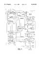
- FIG. 1is block a diagram of a preferred embodiment of the present invention.
- FIG. 2is a more detailed diagram of the circuit of FIG. 1;
- FIG. 3is a more detailed diagram of one of the address generators of FIG. 2;
- FIG. 4is a more detailed diagram of a portion of the circuit of FIG. 2.
- the circuit 50generally comprises an address generator block (or circuit) 52, a memory section (or circuit) 54 and an output section (or circuit) 56.
- the address generator circuit 52may have an input 60 that may receive a clock signal (e.g., CLK), an input 62 that may receive a control signal (e.g., C ⁇ a-n>), an input 64 that may receive an external address signal (e.g., A), an output 66 that may present an internal address signal (e.g., AI) and an output 68 that may present an output selection signal (e.g., OUTSEL).
- the memory section 54may have an input 68 that may receive the internal address signal AI and an output 69 that may present data signals to an input 70 of the output section 56.
- the output section 56may also include an input 74 that may receive the signal CLK, an input 76 that may receive the control (or configuration) signal C ⁇ a-n>, an input 72 that may receive the signal OUTSEL and an output 78 that may present an output signal (e.g., DATAOUT).
- the control signal C ⁇ a-n>may be a multi-bit control signal, where one or more of the bits may be presented to the input 62 and one or more of the bits may be presented to the input 76.
- the one or more bits presented to the input 62may be the same bits or different bits than the one or more bits that may be presented to the input 76.
- the memory section 54generally comprises a memory array 102, an address transition detect (ATD) block (or circuit) 106, a row decode block (or circuit) 108, a bitline load block (or circuit) 110, an equalization block (or circuit) 112, a data buffer block (or circuit) 114, a data line equalization block (or circuit) 116 and a data output block (or circuit) 118.
- ATDaddress transition detect
- the address generator block 52generally comprises a number of address generators 103a-103n.
- Each of the address generators 103a-103ngenerally comprises an X address generator (e.g., 104a), a Z address generator (e.g., 104b) and a Y address generator (e.g., 104c).
- the address generator blocks 104a-104nmay each have an input 120a-120n that may receive the external address A, an input 122a-122n that may receive the external clock signal CLK, an input 124a-124n that may receive the configuration signal C ⁇ a-n>, and an output 126a-126n that may present an internal address signal (e.g., AIa-AIn).
- the internal address signals AIa-AIn presented from the Z address generatorsgenerally comprise a number of select signals (e.g., BLKSEL ⁇ 0>-BLKSEL ⁇ n>) that may be presented to an input 130 of the data buffer block 114.
- the internal address signals AIa-AIn presented from the X address generatorsgenerally comprise a number of select signal (e.g., ROWSEL ⁇ 0>-ROWSEL ⁇ n>) that may be presented to a number of inputs 132a-132n of the row decode block 108.
- the address transition detect block 106generally comprises a number of inputs 134a-134n that may receive the internal address signals AIa-AIn from the X address generators and the Y address generators.
- the address transition detect block 106may also comprise an output 136 that may present a control signal (e.g., an address transition detect signal ATD).
- the signal ATDmay be generated in response to a transition of one of the internal address signals AIa-AIn.
- the signal ATDis generally presented to an input 138 of the equalization block 112 as well as to an input 140 of the data line equalization block 116.
- the input 138is generally shown having an inverter, which generally provides a digital complement (e.g., ATDb) of the signal ATD to the input 138.
- the row decoder block 108generally presents a number of enable signals (e.g., ENa-ENn) at a number of outputs 142a-142n.
- a number of inputs 144a-144n of the memory array 142may receive the enable signals ENa-ENn.
- the enable signals ENa-ENngenerally enable a particular row of the memory array 102 in response to one of the row select signals ROWSEL ⁇ a>-ROWSEL ⁇ n>.
- the memory array 102generally presents a number of bitlines (e.g., BLa-BLBa through BLn-BLBn) at a number of outputs 146a-146n and 148a-148n.
- Datais generally written to or read from the memory array 142 when a voltage difference occurs on a particular bitline pair (e.g., bitlines BLa and BLBa).
- bitline pairs BLa-BLBa through BLn-BLBnrun through the bitline load block 110, the equalization block 112 and to the data buffer block 114.
- One block of the bitlinesgenerally is presented from the data line equalization circuit 116 to the data output circuit 118.
- One block of data outputsis generally presented from the data output block 118.
- the bitline load block 110generally shuts off when a line of a bitline pair BLa-BLBa through BLn-BLBn pulls low so that little or no DC current is supplied by the loads after the bitline is switched.
- the equalization circuit 112generally responds to the signal ATD to provide equalization to the bitlines BLa-BLBa through BLn-BLBn.
- the data buffer block 114generally responds to the signals BLKSEL ⁇ 0>-BLKSEL ⁇ n>to select which bitline pair BLa-BLBa through BLn-BLBn that is reading or writing data to the memory array 102.
- the data line equalization circuit 106generally responds to the address transition detect signal ATD to pre-set the data lines to a known state.
- the data output block 118may have inputs 170a-170n and inputs 172a-172n that generally receive the signals presented at the outputs 160a-160n and 162a-162n of the 20 data line equalization circuit 116.
- the data output block 118 7generally presents a signal at output 180a-180n in response to the signals received at the inputs 170a-170n and 172a-172n.
- the output section 56generally comprises an output multiplexer 181 and an output generator 182.
- the output multiplexergenerally receives the control signal C ⁇ a-n>and the signal OUTSEL ⁇ a-n>from the Y address generators 104a-104n.
- the output multiplexer 181may have an output 184 that presents a signal in response to the control signal C ⁇ a-n>and the signal OUTSEL ⁇ a-n>.
- the output multiplexer 181generally configures the word-width of the signal DATAOUT in response to the control signal C ⁇ a-n>and the clock signal CLK.
- the output multiplexer block 181may receive the output from each data output block 118 and may select which outputs are sent based on the address inputs.
- the configuration signal C ⁇ a-n>may select the word-width of the block (e.g., ⁇ 1, ⁇ 4, ⁇ 8, ⁇ 16 or ⁇ 36).
- the output generator block 182may receive the output (s) from the output multiplexer block 181 and may generate an asynchronous or a synchronous data output based on the configuration signal C ⁇ a-n>and the clock signal CLK (to be described in more detail in connection with FIG. 3).
- the output multiplexer 181 and the output generator 182may each receive one or more of the bits of the control signal C ⁇ a-n>.
- the one or more bits received by the output multiplexer 181may be the same bits or different bits than the one or more bits received by the output generator 182.
- the memory array 102may be designed with a core SRAM device which may be asynchronous having a particular word-width. For example, a word-width of 8-bits may be implemented. However, other word-widths may be implemented to meet the design criteria of a particular implementation. For example, a 32-bit word-width may be implemented. Additional functions may be implemented by the address generator blocks 104a-104n which may control how the inputs and outputs are connected to the memory array 102.
- the address generator 104generally comprises a multiplexer 190 and a register 192.
- the multiplexer 190may comprise an input 194 that may receive the signal A, an input 196 that may receive a signal from the register 192, an input 198 that may receive the control signal C ⁇ a-n>and an output 200 that is generally connected to the output 126 and may provide the internal address signal AI.
- the register 192generally comprises an input 202 that may receive the external address signal A and an output 204 that generally presents a signal to the input 196 of the multiplexer 190.
- the external address Amay be connected to the internal address AI either asynchronously (e.g., when the signal C ⁇ a-n>is low) or synchronously (e.g., when the signal C ⁇ a-n>is high). Therefore, the signal C ⁇ a-n>may control whether the address is asynchronous or synchronous.
- the configuration signal C ⁇ a-n>may either be an input to the address generator 104, or may be the output of a special memory bit which may be used to hold the desired configuration state. It may be desirable for the asynchronous core (i.e., the memory array 102) to have little or no DC current draw when none of the inputs are switching.
- the memory arraymay be implemented as a number of memory cells 220a-220n.
- the bitlines BLa-BLBa through BLn-BLBnmay be implemented as short bitlines. For example, 16 cells may be connected to each pair of bitlines and may be allowed to switch full rail (e.g., from Vss to Vcc). As a result, there may be little or no DC current consumed by the memory cells. Additionally, the short bitlines BLa-BLBa through BLn-BLBn still allow a fast access time.
- the signal ATDmay be used to pre-charge the bitlines BLa-BLBa through BLn-BLBn to VCC after an address change has been detected.
- the bitline load block 110generally comprises a cross-coupled pair of transistors 222 and 224 as well as a half-latch 226 and a half-latch 228.
- the cross-coupled transistors 222 and 224may be implemented as PMOS devices.
- the half-latch 226generally comprises an inverter 230 and a PMOS device 232.
- the half-latch 228generally comprises an inverter 234 and a PMOS device 236.
- the PMOS devices 222, 224, 232 and 236may be implemented as NMOS devices.
- the cross-coupled PMOS devices 222 and 224 and the half-latches 226 and 228may be used as bitline loads.
- the cross-coupled devices 222 and 224 and the half-latches 226 and 228generally shut off when a particular bitline pulls low. As a result, little or no DC current is supplied by the loads after the bitline is switched.
- the equalization circuit 112is shown implemented with a PMOS device 240 and a PMOS device 242.
- NMOS devicesmay be implemented, with the polarity of the signal ATD inverted, such as with an inverter.
- the data buffer block 114a-114nmay be implemented as a tri-state buffer 250 and a tri-state buffer 252.
- the tri-state buffer 250may be implemented as an NMOS device 254, an NMOS device 256 and an PMOS 258.
- the tri-state buffer 252may be implemented as an NMOS device 260, an NMOS device 262 and a PMOS device 264.
- other tri-state buffersmay be implemented accordingly to meet the design criteria of a particular implementation.
- the data buffer circuits 114a-114nmay be implemented in place of a traditional sense-amplifier.
- the tri-state buffer outputs from each set of bitlinesmay be shorted together and drive the data output buffers 118.
- only one set of bitline tri-state buffers 114a114is selected so that only one set of bitline tri-state buffers drives the data output buffers 118.
- the present inventionmay provide the flexibility to be implemented in embedded systems. All of the operational modes (i.e., (i) asynchronous inputs and outputs, (ii) synchronous inputs (e.g., synchronous flowthrough), (iii) synchronous outputs, (iv) synchronous inputs and outputs (e.g., pipelined), (v) a number of bit widths (e.g., ⁇ 32, ⁇ 16, ⁇ 8, ⁇ 4, ⁇ 2, ⁇ 1), (vi) a Read Only Memory (ROM) mode, and/or (vii) a mode implementing a logic function) may be easily configurable within the circuit 50.
- the circuit 100may be used for many more functions than just as a memory storage area (e.g., a logic function implementation is possible).
- circuit 50may use a 1024 ⁇ 8 asynchronous core as the memory array 102.
- any depth/width memorymay be used to implement the memory array 102.
- the word-width of the core memorye.g., ⁇ 8 in one example
- the maximum word-width available for a particular configurationmay be the maximum word-width available for a particular configuration.
- circuit 50with a fully CMOS datapath generally allows both a high speed operation along with a minimal or zero DC power consumption when the inputs are not switching.
- the circuit 100may allow an embedded memory to be used for many different applications which require synchronous memory, asynchronous memory, read-only memory, or random logic functions.
- the present inventionmay give a user the flexibility to use the embedded memory block in a number of configurations.
Landscapes
- Engineering & Computer Science (AREA)
- Microelectronics & Electronic Packaging (AREA)
- Static Random-Access Memory (AREA)
Abstract
Description
Claims (20)
Priority Applications (2)
| Application Number | Priority Date | Filing Date | Title |
|---|---|---|---|
| US09/257,468US6134181A (en) | 1999-02-24 | 1999-02-24 | Configurable memory block |
| US09/690,294US6298005B1 (en) | 1999-02-24 | 2000-10-17 | Configurable memory block |
Applications Claiming Priority (1)
| Application Number | Priority Date | Filing Date | Title |
|---|---|---|---|
| US09/257,468US6134181A (en) | 1999-02-24 | 1999-02-24 | Configurable memory block |
Related Child Applications (1)
| Application Number | Title | Priority Date | Filing Date |
|---|---|---|---|
| US09/690,294ContinuationUS6298005B1 (en) | 1999-02-24 | 2000-10-17 | Configurable memory block |
Publications (1)
| Publication Number | Publication Date |
|---|---|
| US6134181Atrue US6134181A (en) | 2000-10-17 |
Family
ID=22976427
Family Applications (2)
| Application Number | Title | Priority Date | Filing Date |
|---|---|---|---|
| US09/257,468Expired - LifetimeUS6134181A (en) | 1999-02-24 | 1999-02-24 | Configurable memory block |
| US09/690,294Expired - LifetimeUS6298005B1 (en) | 1999-02-24 | 2000-10-17 | Configurable memory block |
Family Applications After (1)
| Application Number | Title | Priority Date | Filing Date |
|---|---|---|---|
| US09/690,294Expired - LifetimeUS6298005B1 (en) | 1999-02-24 | 2000-10-17 | Configurable memory block |
Country Status (1)
| Country | Link |
|---|---|
| US (2) | US6134181A (en) |
Cited By (47)
| Publication number | Priority date | Publication date | Assignee | Title |
|---|---|---|---|---|
| US6298005B1 (en)* | 1999-02-24 | 2001-10-02 | Cypress Semiconductor Corp. | Configurable memory block |
| US6388464B1 (en) | 1999-12-30 | 2002-05-14 | Cypress Semiconductor Corp. | Configurable memory for programmable logic circuits |
| US6466505B1 (en)* | 2001-05-02 | 2002-10-15 | Cypress Semiconductor Corp. | Flexible input structure for an embedded memory |
| US6608500B1 (en) | 2000-03-31 | 2003-08-19 | Cypress Semiconductor Corp. | I/O architecture/cell design for programmable logic device |
| US20040078739A1 (en)* | 1999-11-09 | 2004-04-22 | Kabushiki Kaisha Toshiba | Semiconductor device |
| US6820184B2 (en) | 1999-09-20 | 2004-11-16 | Texas Instruments Incorporated | Memory management in embedded systems with dynamic object instantiation |
| US6864710B1 (en) | 1999-12-30 | 2005-03-08 | Cypress Semiconductor Corp. | Programmable logic device |
| US6968438B1 (en)* | 1999-09-20 | 2005-11-22 | Texas Instruments Incorporated | Application programming interface with inverted memory protocol for embedded software systems |
| US7126398B1 (en) | 2003-12-17 | 2006-10-24 | Cypress Semiconductor Corporation | Method and an apparatus to generate static logic level output |
| US7233540B1 (en)* | 2005-09-27 | 2007-06-19 | Lsi Corporation | Latch-based random access memory (LBRAM) with tri-state banking and contention avoidance |
| US7737724B2 (en) | 2007-04-17 | 2010-06-15 | Cypress Semiconductor Corporation | Universal digital block interconnection and channel routing |
| US7761845B1 (en) | 2002-09-09 | 2010-07-20 | Cypress Semiconductor Corporation | Method for parameterizing a user module |
| US7765095B1 (en) | 2000-10-26 | 2010-07-27 | Cypress Semiconductor Corporation | Conditional branching in an in-circuit emulation system |
| US7770113B1 (en) | 2001-11-19 | 2010-08-03 | Cypress Semiconductor Corporation | System and method for dynamically generating a configuration datasheet |
| US7774190B1 (en) | 2001-11-19 | 2010-08-10 | Cypress Semiconductor Corporation | Sleep and stall in an in-circuit emulation system |
| US7796464B1 (en) | 2003-06-27 | 2010-09-14 | Cypress Semiconductor Corporation | Synchronous memory with a shadow-cycle counter |
| US7825688B1 (en) | 2000-10-26 | 2010-11-02 | Cypress Semiconductor Corporation | Programmable microcontroller architecture(mixed analog/digital) |
| US7844437B1 (en) | 2001-11-19 | 2010-11-30 | Cypress Semiconductor Corporation | System and method for performing next placements and pruning of disallowed placements for programming an integrated circuit |
| US7893724B2 (en) | 2004-03-25 | 2011-02-22 | Cypress Semiconductor Corporation | Method and circuit for rapid alignment of signals |
| US7893772B1 (en) | 2007-12-03 | 2011-02-22 | Cypress Semiconductor Corporation | System and method of loading a programmable counter |
| US8026739B2 (en) | 2007-04-17 | 2011-09-27 | Cypress Semiconductor Corporation | System level interconnect with programmable switching |
| US8040266B2 (en) | 2007-04-17 | 2011-10-18 | Cypress Semiconductor Corporation | Programmable sigma-delta analog-to-digital converter |
| US8049569B1 (en) | 2007-09-05 | 2011-11-01 | Cypress Semiconductor Corporation | Circuit and method for improving the accuracy of a crystal-less oscillator having dual-frequency modes |
| US8069405B1 (en) | 2001-11-19 | 2011-11-29 | Cypress Semiconductor Corporation | User interface for efficiently browsing an electronic document using data-driven tabs |
| US8069428B1 (en) | 2001-10-24 | 2011-11-29 | Cypress Semiconductor Corporation | Techniques for generating microcontroller configuration information |
| US8067948B2 (en) | 2006-03-27 | 2011-11-29 | Cypress Semiconductor Corporation | Input/output multiplexer bus |
| US8069436B2 (en) | 2004-08-13 | 2011-11-29 | Cypress Semiconductor Corporation | Providing hardware independence to automate code generation of processing device firmware |
| US8078894B1 (en) | 2007-04-25 | 2011-12-13 | Cypress Semiconductor Corporation | Power management architecture, method and configuration system |
| US8078970B1 (en) | 2001-11-09 | 2011-12-13 | Cypress Semiconductor Corporation | Graphical user interface with user-selectable list-box |
| US8085100B2 (en) | 2005-02-04 | 2011-12-27 | Cypress Semiconductor Corporation | Poly-phase frequency synthesis oscillator |
| US8085067B1 (en) | 2005-12-21 | 2011-12-27 | Cypress Semiconductor Corporation | Differential-to-single ended signal converter circuit and method |
| US8092083B2 (en) | 2007-04-17 | 2012-01-10 | Cypress Semiconductor Corporation | Temperature sensor with digital bandgap |
| US8103496B1 (en) | 2000-10-26 | 2012-01-24 | Cypress Semicondutor Corporation | Breakpoint control in an in-circuit emulation system |
| US8103497B1 (en) | 2002-03-28 | 2012-01-24 | Cypress Semiconductor Corporation | External interface for event architecture |
| US8120408B1 (en) | 2005-05-05 | 2012-02-21 | Cypress Semiconductor Corporation | Voltage controlled oscillator delay cell and method |
| US8130025B2 (en) | 2007-04-17 | 2012-03-06 | Cypress Semiconductor Corporation | Numerical band gap |
| US8149048B1 (en) | 2000-10-26 | 2012-04-03 | Cypress Semiconductor Corporation | Apparatus and method for programmable power management in a programmable analog circuit block |
| US8176296B2 (en) | 2000-10-26 | 2012-05-08 | Cypress Semiconductor Corporation | Programmable microcontroller architecture |
| US8402313B1 (en) | 2002-05-01 | 2013-03-19 | Cypress Semiconductor Corporation | Reconfigurable testing system and method |
| US8499270B1 (en) | 2007-04-25 | 2013-07-30 | Cypress Semiconductor Corporation | Configuration of programmable IC design elements |
| US8516025B2 (en) | 2007-04-17 | 2013-08-20 | Cypress Semiconductor Corporation | Clock driven dynamic datapath chaining |
| US8527949B1 (en) | 2001-11-19 | 2013-09-03 | Cypress Semiconductor Corporation | Graphical user interface for dynamically reconfiguring a programmable device |
| US20140247672A1 (en)* | 2010-10-20 | 2014-09-04 | Taiwan Semiconductor Manufacturing Company, Ltd. | Reading memory data |
| US9448964B2 (en) | 2009-05-04 | 2016-09-20 | Cypress Semiconductor Corporation | Autonomous control in a programmable system |
| US9564902B2 (en) | 2007-04-17 | 2017-02-07 | Cypress Semiconductor Corporation | Dynamically configurable and re-configurable data path |
| US9720805B1 (en) | 2007-04-25 | 2017-08-01 | Cypress Semiconductor Corporation | System and method for controlling a target device |
| US10698662B2 (en) | 2001-11-15 | 2020-06-30 | Cypress Semiconductor Corporation | System providing automatic source code generation for personalization and parameterization of user modules |
Families Citing this family (6)
| Publication number | Priority date | Publication date | Assignee | Title |
|---|---|---|---|---|
| KR100320683B1 (en)* | 2000-02-03 | 2002-01-17 | 윤종용 | Semiconductor memory device with function for repairing stand-by current fail |
| US7061792B1 (en) | 2002-08-10 | 2006-06-13 | National Semiconductor Corporation | Low AC power SRAM architecture |
| US7286383B1 (en)* | 2002-08-10 | 2007-10-23 | National Semiconductor Corporation | Bit line sharing and word line load reduction for low AC power SRAM architecture |
| US6721224B2 (en) | 2002-08-26 | 2004-04-13 | Mosel Vitelic, Inc. | Memory refresh methods and circuits |
| TW201135747A (en)* | 2010-04-13 | 2011-10-16 | Novatek Microelectronics Corp | Embedded storage apparatus and test method thereof |
| US8400863B1 (en)* | 2010-08-20 | 2013-03-19 | Altera Corporation | Configurable memory block |
Citations (1)
| Publication number | Priority date | Publication date | Assignee | Title |
|---|---|---|---|---|
| US5384745A (en)* | 1992-04-27 | 1995-01-24 | Mitsubishi Denki Kabushiki Kaisha | Synchronous semiconductor memory device |
Family Cites Families (2)
| Publication number | Priority date | Publication date | Assignee | Title |
|---|---|---|---|---|
| US5835970A (en) | 1995-12-21 | 1998-11-10 | Cypress Semiconductor Corp. | Burst address generator having two modes of operation employing a linear/nonlinear counter using decoded addresses |
| US6134181A (en)* | 1999-02-24 | 2000-10-17 | Cypress Semiconductor Corp. | Configurable memory block |
- 1999
- 1999-02-24USUS09/257,468patent/US6134181A/ennot_activeExpired - Lifetime
- 2000
- 2000-10-17USUS09/690,294patent/US6298005B1/ennot_activeExpired - Lifetime
Patent Citations (1)
| Publication number | Priority date | Publication date | Assignee | Title |
|---|---|---|---|---|
| US5384745A (en)* | 1992-04-27 | 1995-01-24 | Mitsubishi Denki Kabushiki Kaisha | Synchronous semiconductor memory device |
Cited By (67)
| Publication number | Priority date | Publication date | Assignee | Title |
|---|---|---|---|---|
| US6298005B1 (en)* | 1999-02-24 | 2001-10-02 | Cypress Semiconductor Corp. | Configurable memory block |
| US6820184B2 (en) | 1999-09-20 | 2004-11-16 | Texas Instruments Incorporated | Memory management in embedded systems with dynamic object instantiation |
| US6968438B1 (en)* | 1999-09-20 | 2005-11-22 | Texas Instruments Incorporated | Application programming interface with inverted memory protocol for embedded software systems |
| US7146546B2 (en)* | 1999-11-09 | 2006-12-05 | Kabushiki Kaisha Toshiba | Semiconductor device |
| US20040078739A1 (en)* | 1999-11-09 | 2004-04-22 | Kabushiki Kaisha Toshiba | Semiconductor device |
| US6388464B1 (en) | 1999-12-30 | 2002-05-14 | Cypress Semiconductor Corp. | Configurable memory for programmable logic circuits |
| US6512395B1 (en) | 1999-12-30 | 2003-01-28 | Cypress Semiconductor Corp. | Configurable memory for programmable logic circuits |
| US6864710B1 (en) | 1999-12-30 | 2005-03-08 | Cypress Semiconductor Corp. | Programmable logic device |
| US6608500B1 (en) | 2000-03-31 | 2003-08-19 | Cypress Semiconductor Corp. | I/O architecture/cell design for programmable logic device |
| US7765095B1 (en) | 2000-10-26 | 2010-07-27 | Cypress Semiconductor Corporation | Conditional branching in an in-circuit emulation system |
| US8555032B2 (en) | 2000-10-26 | 2013-10-08 | Cypress Semiconductor Corporation | Microcontroller programmable system on a chip with programmable interconnect |
| US8103496B1 (en) | 2000-10-26 | 2012-01-24 | Cypress Semicondutor Corporation | Breakpoint control in an in-circuit emulation system |
| US8149048B1 (en) | 2000-10-26 | 2012-04-03 | Cypress Semiconductor Corporation | Apparatus and method for programmable power management in a programmable analog circuit block |
| US10261932B2 (en) | 2000-10-26 | 2019-04-16 | Cypress Semiconductor Corporation | Microcontroller programmable system on a chip |
| US8176296B2 (en) | 2000-10-26 | 2012-05-08 | Cypress Semiconductor Corporation | Programmable microcontroller architecture |
| US10248604B2 (en) | 2000-10-26 | 2019-04-02 | Cypress Semiconductor Corporation | Microcontroller programmable system on a chip |
| US10020810B2 (en) | 2000-10-26 | 2018-07-10 | Cypress Semiconductor Corporation | PSoC architecture |
| US9843327B1 (en) | 2000-10-26 | 2017-12-12 | Cypress Semiconductor Corporation | PSOC architecture |
| US7825688B1 (en) | 2000-10-26 | 2010-11-02 | Cypress Semiconductor Corporation | Programmable microcontroller architecture(mixed analog/digital) |
| US9766650B2 (en) | 2000-10-26 | 2017-09-19 | Cypress Semiconductor Corporation | Microcontroller programmable system on a chip with programmable interconnect |
| US8358150B1 (en) | 2000-10-26 | 2013-01-22 | Cypress Semiconductor Corporation | Programmable microcontroller architecture(mixed analog/digital) |
| US8736303B2 (en) | 2000-10-26 | 2014-05-27 | Cypress Semiconductor Corporation | PSOC architecture |
| US10725954B2 (en) | 2000-10-26 | 2020-07-28 | Monterey Research, Llc | Microcontroller programmable system on a chip |
| US6466505B1 (en)* | 2001-05-02 | 2002-10-15 | Cypress Semiconductor Corp. | Flexible input structure for an embedded memory |
| US8793635B1 (en) | 2001-10-24 | 2014-07-29 | Cypress Semiconductor Corporation | Techniques for generating microcontroller configuration information |
| US8069428B1 (en) | 2001-10-24 | 2011-11-29 | Cypress Semiconductor Corporation | Techniques for generating microcontroller configuration information |
| US10466980B2 (en) | 2001-10-24 | 2019-11-05 | Cypress Semiconductor Corporation | Techniques for generating microcontroller configuration information |
| US8078970B1 (en) | 2001-11-09 | 2011-12-13 | Cypress Semiconductor Corporation | Graphical user interface with user-selectable list-box |
| US10698662B2 (en) | 2001-11-15 | 2020-06-30 | Cypress Semiconductor Corporation | System providing automatic source code generation for personalization and parameterization of user modules |
| US8527949B1 (en) | 2001-11-19 | 2013-09-03 | Cypress Semiconductor Corporation | Graphical user interface for dynamically reconfiguring a programmable device |
| US8533677B1 (en) | 2001-11-19 | 2013-09-10 | Cypress Semiconductor Corporation | Graphical user interface for dynamically reconfiguring a programmable device |
| US7770113B1 (en) | 2001-11-19 | 2010-08-03 | Cypress Semiconductor Corporation | System and method for dynamically generating a configuration datasheet |
| US7774190B1 (en) | 2001-11-19 | 2010-08-10 | Cypress Semiconductor Corporation | Sleep and stall in an in-circuit emulation system |
| US7844437B1 (en) | 2001-11-19 | 2010-11-30 | Cypress Semiconductor Corporation | System and method for performing next placements and pruning of disallowed placements for programming an integrated circuit |
| US8370791B2 (en) | 2001-11-19 | 2013-02-05 | Cypress Semiconductor Corporation | System and method for performing next placements and pruning of disallowed placements for programming an integrated circuit |
| US8069405B1 (en) | 2001-11-19 | 2011-11-29 | Cypress Semiconductor Corporation | User interface for efficiently browsing an electronic document using data-driven tabs |
| US8103497B1 (en) | 2002-03-28 | 2012-01-24 | Cypress Semiconductor Corporation | External interface for event architecture |
| US8402313B1 (en) | 2002-05-01 | 2013-03-19 | Cypress Semiconductor Corporation | Reconfigurable testing system and method |
| US7761845B1 (en) | 2002-09-09 | 2010-07-20 | Cypress Semiconductor Corporation | Method for parameterizing a user module |
| US7796464B1 (en) | 2003-06-27 | 2010-09-14 | Cypress Semiconductor Corporation | Synchronous memory with a shadow-cycle counter |
| US7126398B1 (en) | 2003-12-17 | 2006-10-24 | Cypress Semiconductor Corporation | Method and an apparatus to generate static logic level output |
| US7893724B2 (en) | 2004-03-25 | 2011-02-22 | Cypress Semiconductor Corporation | Method and circuit for rapid alignment of signals |
| US8069436B2 (en) | 2004-08-13 | 2011-11-29 | Cypress Semiconductor Corporation | Providing hardware independence to automate code generation of processing device firmware |
| US8085100B2 (en) | 2005-02-04 | 2011-12-27 | Cypress Semiconductor Corporation | Poly-phase frequency synthesis oscillator |
| US8120408B1 (en) | 2005-05-05 | 2012-02-21 | Cypress Semiconductor Corporation | Voltage controlled oscillator delay cell and method |
| US7233540B1 (en)* | 2005-09-27 | 2007-06-19 | Lsi Corporation | Latch-based random access memory (LBRAM) with tri-state banking and contention avoidance |
| US8085067B1 (en) | 2005-12-21 | 2011-12-27 | Cypress Semiconductor Corporation | Differential-to-single ended signal converter circuit and method |
| US8067948B2 (en) | 2006-03-27 | 2011-11-29 | Cypress Semiconductor Corporation | Input/output multiplexer bus |
| US8717042B1 (en) | 2006-03-27 | 2014-05-06 | Cypress Semiconductor Corporation | Input/output multiplexer bus |
| US8476928B1 (en) | 2007-04-17 | 2013-07-02 | Cypress Semiconductor Corporation | System level interconnect with programmable switching |
| US8026739B2 (en) | 2007-04-17 | 2011-09-27 | Cypress Semiconductor Corporation | System level interconnect with programmable switching |
| US8130025B2 (en) | 2007-04-17 | 2012-03-06 | Cypress Semiconductor Corporation | Numerical band gap |
| US7737724B2 (en) | 2007-04-17 | 2010-06-15 | Cypress Semiconductor Corporation | Universal digital block interconnection and channel routing |
| US8482313B2 (en) | 2007-04-17 | 2013-07-09 | Cypress Semiconductor Corporation | Universal digital block interconnection and channel routing |
| US8516025B2 (en) | 2007-04-17 | 2013-08-20 | Cypress Semiconductor Corporation | Clock driven dynamic datapath chaining |
| US8040266B2 (en) | 2007-04-17 | 2011-10-18 | Cypress Semiconductor Corporation | Programmable sigma-delta analog-to-digital converter |
| US8092083B2 (en) | 2007-04-17 | 2012-01-10 | Cypress Semiconductor Corporation | Temperature sensor with digital bandgap |
| US9564902B2 (en) | 2007-04-17 | 2017-02-07 | Cypress Semiconductor Corporation | Dynamically configurable and re-configurable data path |
| US9720805B1 (en) | 2007-04-25 | 2017-08-01 | Cypress Semiconductor Corporation | System and method for controlling a target device |
| US8909960B1 (en) | 2007-04-25 | 2014-12-09 | Cypress Semiconductor Corporation | Power management architecture, method and configuration system |
| US8499270B1 (en) | 2007-04-25 | 2013-07-30 | Cypress Semiconductor Corporation | Configuration of programmable IC design elements |
| US8078894B1 (en) | 2007-04-25 | 2011-12-13 | Cypress Semiconductor Corporation | Power management architecture, method and configuration system |
| US8049569B1 (en) | 2007-09-05 | 2011-11-01 | Cypress Semiconductor Corporation | Circuit and method for improving the accuracy of a crystal-less oscillator having dual-frequency modes |
| US7893772B1 (en) | 2007-12-03 | 2011-02-22 | Cypress Semiconductor Corporation | System and method of loading a programmable counter |
| US9448964B2 (en) | 2009-05-04 | 2016-09-20 | Cypress Semiconductor Corporation | Autonomous control in a programmable system |
| US9183903B2 (en)* | 2010-10-20 | 2015-11-10 | Taiwan Semiconductor Manufacturing Company, Ltd. | Reading memory data |
| US20140247672A1 (en)* | 2010-10-20 | 2014-09-04 | Taiwan Semiconductor Manufacturing Company, Ltd. | Reading memory data |
Also Published As
| Publication number | Publication date |
|---|---|
| US6298005B1 (en) | 2001-10-02 |
Similar Documents
| Publication | Publication Date | Title |
|---|---|---|
| US6134181A (en) | Configurable memory block | |
| KR0142805B1 (en) | Semiconductor memory device | |
| US7345936B2 (en) | Data storage circuit | |
| US11527282B2 (en) | SRAM with burst mode operation | |
| KR970004416B1 (en) | Random-access memory and its read and write circuit as well as read and write method of data packet | |
| JP3754593B2 (en) | Integrated circuit having memory cells for storing data bits and method for writing write data bits to memory cells in integrated circuits | |
| US10885982B2 (en) | Semiconductor memory device and control method therefor | |
| WO2005006340A2 (en) | Sram cell structure and circuits | |
| USRE36655E (en) | Semiconductor memory device and method for reading and writing data therein | |
| JPH05334876A (en) | Semiconductor memory having memory row line selecting latch type repeater | |
| US7599237B2 (en) | Memory device and method for precharging a memory device | |
| US5963484A (en) | High speed single-ended amplifier of a latched type | |
| EP0547889B1 (en) | A tristatable driver for internal data bus lines | |
| US6484231B1 (en) | Synchronous SRAM circuit | |
| US5295104A (en) | Integrated circuit with precharged internal data bus | |
| JP2588936B2 (en) | Semiconductor storage device | |
| EP0952549B1 (en) | Edge transition detection disable circuit to alter memory device operating characteristics | |
| EP0547892B1 (en) | An integrated circuit with self-biased differential data lines | |
| US6741493B1 (en) | Split local and continuous bitline requiring fewer wires | |
| US6597201B1 (en) | Dynamic predecoder circuitry for memory circuits | |
| KR100340067B1 (en) | Memory device having single port memory capable of reading and writing data at the same time | |
| KR100298181B1 (en) | Register file having a plurality of read/write and bypass path | |
| US6580656B2 (en) | Semiconductor memory device having memory cell block activation control circuit and method for controlling activation of memory cell blocks thereof | |
| US11462263B2 (en) | Burst-mode memory with column multiplexer | |
| KR100431304B1 (en) | A static random access memory with improved read performance |
Legal Events
| Date | Code | Title | Description |
|---|---|---|---|
| AS | Assignment | Owner name:MICRON TECHNOLOGY, INC., IDAHO Free format text:ASSIGNMENT OF ASSIGNORS INTEREST;ASSIGNORS:FORBES, LEONARD;AHN, KIE Y.;REEL/FRAME:009795/0334;SIGNING DATES FROM 19990219 TO 19990222 Owner name:CYPRESS SEMICONDUCTOR CORPORATION, CALIFORNIA Free format text:ASSIGNMENT OF ASSIGNORS INTEREST;ASSIGNOR:LANDRY, GREG J.;REEL/FRAME:009802/0301 Effective date:19990224 | |
| STCF | Information on status: patent grant | Free format text:PATENTED CASE | |
| FPAY | Fee payment | Year of fee payment:4 | |
| FPAY | Fee payment | Year of fee payment:8 | |
| FPAY | Fee payment | Year of fee payment:12 | |
| AS | Assignment | Owner name:MORGAN STANLEY SENIOR FUNDING, INC., NEW YORK Free format text:SECURITY INTEREST;ASSIGNORS:CYPRESS SEMICONDUCTOR CORPORATION;SPANSION LLC;REEL/FRAME:035240/0429 Effective date:20150312 | |
| AS | Assignment | Owner name:SPANSION LLC, CALIFORNIA Free format text:PARTIAL RELEASE OF SECURITY INTEREST IN PATENTS;ASSIGNOR:MORGAN STANLEY SENIOR FUNDING, INC., AS COLLATERAL AGENT;REEL/FRAME:039708/0001 Effective date:20160811 Owner name:CYPRESS SEMICONDUCTOR CORPORATION, CALIFORNIA Free format text:PARTIAL RELEASE OF SECURITY INTEREST IN PATENTS;ASSIGNOR:MORGAN STANLEY SENIOR FUNDING, INC., AS COLLATERAL AGENT;REEL/FRAME:039708/0001 Effective date:20160811 | |
| AS | Assignment | Owner name:MONTEREY RESEARCH, LLC, CALIFORNIA Free format text:ASSIGNMENT OF ASSIGNORS INTEREST;ASSIGNOR:CYPRESS SEMICONDUCTOR CORPORATION;REEL/FRAME:040911/0238 Effective date:20160811 | |
| AS | Assignment | Owner name:MORGAN STANLEY SENIOR FUNDING, INC., NEW YORK Free format text:CORRECTIVE ASSIGNMENT TO CORRECT THE 8647899 PREVIOUSLY RECORDED ON REEL 035240 FRAME 0429. ASSIGNOR(S) HEREBY CONFIRMS THE SECURITY INTERST;ASSIGNORS:CYPRESS SEMICONDUCTOR CORPORATION;SPANSION LLC;REEL/FRAME:058002/0470 Effective date:20150312 |