US6134090A - Enhanced spin-valve/GMR magnetic sensor with an insulating boundary layer - Google Patents
Enhanced spin-valve/GMR magnetic sensor with an insulating boundary layerDownload PDFInfo
- Publication number
- US6134090A US6134090AUS09/153,581US15358198AUS6134090AUS 6134090 AUS6134090 AUS 6134090AUS 15358198 AUS15358198 AUS 15358198AUS 6134090 AUS6134090 AUS 6134090A
- Authority
- US
- United States
- Prior art keywords
- layer
- ferromagnetic
- spin valve
- valve sensor
- ferromagnetic material
- Prior art date
- Legal status (The legal status is an assumption and is not a legal conclusion. Google has not performed a legal analysis and makes no representation as to the accuracy of the status listed.)
- Expired - Lifetime
Links
Images


Classifications
- G—PHYSICS
- G11—INFORMATION STORAGE
- G11B—INFORMATION STORAGE BASED ON RELATIVE MOVEMENT BETWEEN RECORD CARRIER AND TRANSDUCER
- G11B5/00—Recording by magnetisation or demagnetisation of a record carrier; Reproducing by magnetic means; Record carriers therefor
- G11B5/127—Structure or manufacture of heads, e.g. inductive
- G11B5/33—Structure or manufacture of flux-sensitive heads, i.e. for reproduction only; Combination of such heads with means for recording or erasing only
- G11B5/39—Structure or manufacture of flux-sensitive heads, i.e. for reproduction only; Combination of such heads with means for recording or erasing only using magneto-resistive devices or effects
- G11B5/3903—Structure or manufacture of flux-sensitive heads, i.e. for reproduction only; Combination of such heads with means for recording or erasing only using magneto-resistive devices or effects using magnetic thin film layers or their effects, the films being part of integrated structures
- B—PERFORMING OPERATIONS; TRANSPORTING
- B82—NANOTECHNOLOGY
- B82Y—SPECIFIC USES OR APPLICATIONS OF NANOSTRUCTURES; MEASUREMENT OR ANALYSIS OF NANOSTRUCTURES; MANUFACTURE OR TREATMENT OF NANOSTRUCTURES
- B82Y10/00—Nanotechnology for information processing, storage or transmission, e.g. quantum computing or single electron logic
- B—PERFORMING OPERATIONS; TRANSPORTING
- B82—NANOTECHNOLOGY
- B82Y—SPECIFIC USES OR APPLICATIONS OF NANOSTRUCTURES; MEASUREMENT OR ANALYSIS OF NANOSTRUCTURES; MANUFACTURE OR TREATMENT OF NANOSTRUCTURES
- B82Y25/00—Nanomagnetism, e.g. magnetoimpedance, anisotropic magnetoresistance, giant magnetoresistance or tunneling magnetoresistance
- G—PHYSICS
- G01—MEASURING; TESTING
- G01R—MEASURING ELECTRIC VARIABLES; MEASURING MAGNETIC VARIABLES
- G01R33/00—Arrangements or instruments for measuring magnetic variables
- G01R33/02—Measuring direction or magnitude of magnetic fields or magnetic flux
- G01R33/06—Measuring direction or magnitude of magnetic fields or magnetic flux using galvano-magnetic devices
- G01R33/09—Magnetoresistive devices
- G01R33/093—Magnetoresistive devices using multilayer structures, e.g. giant magnetoresistance sensors
- G—PHYSICS
- G11—INFORMATION STORAGE
- G11B—INFORMATION STORAGE BASED ON RELATIVE MOVEMENT BETWEEN RECORD CARRIER AND TRANSDUCER
- G11B5/00—Recording by magnetisation or demagnetisation of a record carrier; Reproducing by magnetic means; Record carriers therefor
- G11B5/127—Structure or manufacture of heads, e.g. inductive
- G11B5/33—Structure or manufacture of flux-sensitive heads, i.e. for reproduction only; Combination of such heads with means for recording or erasing only
- G11B5/39—Structure or manufacture of flux-sensitive heads, i.e. for reproduction only; Combination of such heads with means for recording or erasing only using magneto-resistive devices or effects
- G11B2005/3996—Structure or manufacture of flux-sensitive heads, i.e. for reproduction only; Combination of such heads with means for recording or erasing only using magneto-resistive devices or effects large or giant magnetoresistive effects [GMR], e.g. as generated in spin-valve [SV] devices
Definitions
- the inventionrelates to spin valve sensors for use in magnetic disc read/write heads.
- Magnetic sensors utilizing giant magnetoresistance (GMR) effectshave utility as magnetic sensors, especially in magnetoresistive read heads used in magnetic disc storage systems.
- the GMR effectis observed in ultrathin, electrically conductive multilayer systems having magnetic layers.
- Magnetic sensors utilizing the GMR effectare frequently referred to as "spin valve" sensors.
- a spin valve sensoris typically a sandwiched structure including two ferromagnetic layers separated by a thin non-ferromagnetic layer.
- One of the ferromagnetic layersis called the "pinned layer” because it is magnetically pinned or oriented in a fixed and unchanging direction.
- One common method of maintaining the magnetic orientation of the pinning layeris through anti-ferromagnetic exchange coupling utilizing a proximate, i.e. adjacent or nearby, anti-ferromagnetic layer, commonly referred to as the "pinning layer.”
- the other ferromagnetic layeris called the “free” or “unpinned” layer because its magnetization can rotate in response to the presence of external magnetic fields.
- spin valve sensorsresult from a large difference in electrical conductivity exhibited by the devices depending on the relative alignment between the magnetizations of the two ferromagnetic layers.
- a sufficient pinning field from the pinning layeris required to keep the pinned ferromagnetic layer's magnetization unchanged during operation.
- Various anti-ferromagnetic materialssuch as NiMn, FeMn, NiO, IrMn, PtPdMn, CrMnPt, RuRhMn, and TbCo, have been used or proposed as antiferromagnetic pinning layers for spin valve sensors
- the inventionfeatures a spin valve sensor comprising:
- the inventionfeatures a method of producing a spin valve sensor, the method comprising:
- the multilayer structurecomprising:
- a spacer layer of electrically conducting, non-ferromagnetic materialpositioned between the first and second layers of ferromagnetic material
- a pinning layercomprising manganese, proximate the first ferromagnetic layer and opposite the spacer layer;
- FIG. 1is a schematic, top view of a disc drive system.
- FIG. 2is a schematic, perspective view of a slider with a spin valve/GMR sensor.
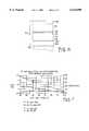
- FIG. 3is a schematic, fragmentary, side view of a spin valve/GMR sensor on a substrate.
- FIG. 4is a schematic, fragmentary, side view of an embodiment of the spin valve/GMR sensor of FIG. 3 with ferromagnetic layers having two component layers each.
- FIG. 5is a schematic, fragmentary, side view of an embodiment of the spin valve/GMR sensor of FIG. 3 with ferromagnetic layers having three component layers each.
- FIG. 6is a schematic, fragmentary, side view of a top spin valve/GMR sensor on a substrate.
- FIG. 7is a plot of GMR effect in percent and change in resistance (dR in milliohms) from varying the orientation of an external magnetic field both as a function of NiFe free layer thickness for a spin valve/GMR sensor of FIG. 5 and for a corresponding spin valve with a Ta cap.
- a relevant spin valve GMRgenerally includes an antiferromagnetic pinning layer, a first or pinned ferromagnetic layer proximate the pinning layer, a second or free ferromagnetic layer and a non-ferromagnetic layer between the first and second ferromagnetic layers.
- the spin valveis referred to as a bottom spin valve.
- the free ferromagnetic layeris at the top of the spin valve structure so that thin electrically insulating layers can be generated at its surface without affecting the stacks below.
- the free ferromagnetic layeris at the bottom of the spin valve structure proximate to a substrate.
- the pinning layeris placed proximate to a substrate such that the deposition of a thin insulating layer adjacent to the free ferromagnetic layer does not disrupt the crystal lattice of the other layers of the spin valve.
- Other embodimentsinclude symmetric spin valves having two pinning layers with one on either side of the spin valve and duplicate pinned ferromagnetic layers and duplicate spacer layers in a symmetric arrangement.
- the presence of the electrically insulating layer adjacent to the free ferromagnetic layerevidently generates flatter electronic surfaces, which promote the specular scattering of electrons.
- the GMR effectresults from reduced scattering of conduction electrons when the magnetic fields of the two ferromagnetic layers are aligned. At the edge of the ferromagnetic layer, diffusive or specular scattering can occur. Diffusive scattering results in the loss of momentum and spin coherence. In contrast, specular scattering preserve momentum and spin coherence. Thus, increased specular scattering of electrons at the edge of the free ferromagnetic material results in the enhanced GMR effect.
- FIG. 1depicts an embodiment of a disc drive system 100 including drive unit 102, actuator assembly 104 and controller 106.
- Drive unit 102includes disc 108 and spindle 110 connected to a spindle motor.
- actuator assembly 104includes actuator 112, support arm 114, load beam 116 and gimble/head assembly 118.
- Actuator 112controls the position of gimble/head assembly 118 over disc 108 by rotating or laterally moving support arm 114.
- Load beam 116is located at the end of support arm 114 and gimble/head assembly 118 is located at the end of load beam 116.
- Controller 106instructs actuator 112 regarding the position of support arm 114 over disc 108 and drive unit 102 regarding the control of the spindle motor.
- Gimble/head assembly 118includes a slider which, in operation, flies just above the disc surface.
- FIG. 2depicts an embodiment of a slider 140.
- glider 140includes two rails 142, 144 oriented along the length of air bearing surface 146.
- Other structure in addition or alternative to rails 142, 144can be contoured into the air bearing surface to alter the aerodynamic performance of slider 140.
- GMR spin valve 150is located at or near the rear edge of slider 140.
- the spin valveis deposited in layer onto the slider body.
- the substrate, on which the spin valve is depositedis an electrically insulating layer that forms a boundary of the spin valve referred to as a 1st half gap. Additional layers such as an Al 2 O 3 base coat and a bottom shield can be placed between the 1st half gap and the slider body.
- An electrically insulating layer referred to as a second half gapis placed over the spin valve. The entire structure is covered at its top surface with a top shield or shared pole.
- a preferred embodiment of spin valve 150is located on a substrate 202.
- Substrate 202preferably is a layer of Al 2 O 3 , aluminum nitride, diamond-like carbon or other electrically insulating material.
- Substrate 202is referred to as a first half gap and is oriented toward the slider body.
- Spin valve 150includes an optional seed layer 204, pinning layer 210, pinned ferromagnetic layer 212, spacer layer 214, free ferromagnetic layer 216, electrically insulating layer 218 and electrically insulating layer 220.
- a second half gap 222is located over the spin valve.
- Seed layer 204provides a transition between the crystal lattice of the adjacent spin valve layers and the lattice of the substrate such that the crystal lattice of the spin valve layers is not significantly disrupted at the interface.
- Suitable materials for the seed layerinclude, for example, tantalum (Ta) and bilayers of Ta and NiFe.
- Ta seed layersgenerally have a thickness on the order of about 35 ⁇ . Other materials and thicknesses can be used as appropriate.
- Pinning layer 210is an antiferromagnetic layer. Suitable antiferromagnetic materials for the pinning layer include, for example, the following manganese alloys: NiMn, FeMn, IrMn, PtPdMn, RuMn, RhMn and CrMnPt. The use of NiMn pinning layers is described in U.S. Pat. No. 5,764,056, entitled “Nickel-Manganese Pinned Spin Valve/GMR Magnetic Sensors,” incorporated herein by reference. Pinning layer 210 preferably has a thickness from about 80 ⁇ to about 500 ⁇ , and more preferably from about 100 ⁇ to about 300 ⁇ .
- Spacer layer 214is made from non-ferromagnetic, electrically conducting material. Spacer layer magnetically uncouples pinned ferromagnetic layer 212 from free ferromagnetic layer 216.
- a variety of non-ferromagnetic, electrically conducting materialscan be used for spacer layer 214. Preferred materials for spacer layer 214 include, for example, copper, CuAu and CuAg.
- Spacer layer 214generally has a thickness from about 25 ⁇ to about 50 ⁇ . In preferred embodiments, spacer layer 214 is a layer of copper with a thickness from about 25 ⁇ to about 35 ⁇ .
- Ferromagnetic layers 212, 216can be single layer or, preferably, multilayered structures. Suitable ferromagnetic, electrically conducting materials for the formation of ferromagnetic layers 212, 216 include, for example, Co, NiFe, CoFe, CoZrNb, NiFeCr, AlSiFe and NiFeRe. The arrangement of component layers, number of component layers and thickness of component layers within ferromagnetic layers 212, 216 can be adjusted to achieve desired characteristics.
- ferromagnetic layers 212, 216are a single layer of ferromagnetic material, as shown in FIG. 3.
- ferromagnetic layers 212, 216each can have two component layers of ferromagnetic material 230, 232 and 234, 236, as shown in FIG. 4.
- layers 230 and 236are cobalt with a thickness of about 15 ⁇
- layers 232 and 234are NiFe with a thickness of about 50 ⁇ .
- ferromagnetic layer 212has three component layers 240, 242, 244, and ferromagnetic layer 216 has three component layers 250, 252, 254, see FIG. 5.
- component layers 240 and 254are CoFe alloy with a thickness of about 30 ⁇ .
- Component layers 242, 252are NiFe with a thickness of about 30 ⁇ .
- Component layers 244 and 250are cobalt with a thickness of about 20 ⁇ .
- Ferromagnetic layers 212, 216do not have necessarily the same number, composition and/or thickness of the component layers as each other.
- the orientation of the magnetic moment of pinned ferromagnetic layer 212is fixed by its proximity to pinning layer 210.
- the orientation of free ferromagnetic layer 216is oriented by the magnetic moment of the disc surface as the slider flies over the magnetic disc.
- the relative orientation of the magnetic moment in the pinned ferromagnetic layer and in the free ferromagnetic layerresults in the Giant Magneto-Resistive (GMR) effect when the layers have sufficient thinness and the materials are properly selected.
- GMRGiant Magneto-Resistive
- Electrically insulating layer 218preferably is an oxide layer formed by oxidizing the top portion of ferromagnetic layer 216.
- the electrically insulating nature of layer 218generates flatter electronic surfaces that promote specular scattering of conduction electrons. This specular scattering leads to an observed enhanced GMR effect.
- the oxide layercan be formed using an oxygen plasma formed by application of a voltage to ferromagnetic layer 216 in an oxygen atmosphere.
- an oxide layercan be formed by thermal oxidation obtained by heating ferromagnetic layer 216 under an oxygen atmosphere.
- the oxide layercan be formed by sputtering a portion of ferromagnetic layer 216 in the presence of an oxygen atmosphere (reactive sputtering) rather than an inert atmosphere or vacuum.
- oxide layer 218has an average thickness of about 2 monolayers to about 10 monolayers and more preferably 3 to 5 monolayers, although the oxide layer may not be flat especially if the ferromagnetic layer on which the oxide layer is placed is not flat. Excessive oxidation should be avoided so that the free ferromagnetic layer is not completely or mostly oxidized. Oxidation times can be determined empirically for a particular oxygen concentration and a particular oxidation approach.
- electrically insulating layer 218is formed by the deposition of an oxide such as NiFeO x that forms a continuous transition between the two substances at the interface with a ferromagnetic material such as NiFe.
- a ferromagnetic materialsuch as NiFe.
- Other electrically insulating materialscan be used such as Al 2 O 3 , Ta 2 O 5 , carbon nitride and diamond-like carbon.
- Preferred materials for electrically insulating layer 218may effectively oxidize rough portions of the free ferromagnetic layer to produce specular scattering of electrons.
- vacuumis not broken between the formation of free ferromagnetic layer 216 and electrically insulating layer 218, although oxygen can be bled selectively into the system at low pressures.
- electrically insulating layer 220can be produced from any convenient electrically insulating material.
- layer 220can be an oxide layer, Al 2 O 3 , Ta 2 O 5 , carbon nitride or diamond-like carbon.
- Layer 220preferably has a thickness from about 2 monolayers to about 5 nm.
- FIG. 7displays plots of the GMR effect and of the change in resistance resulting from changing the orientation of the applied magnetic field from parallel to antiparallel.
- the results marked as not having a Ta capwere measured with a GMR spin valve essentially as shown in FIG. 5.
- the spin valves used to produce FIG. 7included a NiMn pinning layer and were annealed as described below. For comparison, results were obtained with a GMR spin valve with comparable pinning layer, ferromagnetic layers and spacer layer as shown in FIG. 5 with the oxide layer replaced with a Ta cap with a thickness of about 50 ⁇ .
- the spin valveswere completed with the addition of a 2nd half gap and a shield.
- Additional spin valveswere tested with two component layer ferromagnetic layers to evaluate the effect of replacing a Ta cap with an oxide layer. These spin valves again had a NiMn pinning layer and were annealed. A first pair of additional spin valves had a 31 nm copper spacing layer and ferromagnetic layers formed from 10 nm of Co and 60 nm of NiFe. The measurements made using these spin valves with an oxide layer or a Ta cap are shown in Table 1.
- a second pair of spin valveshad a 34 nm copper spacer layer and ferromagnetic layers formed from 10 nm Co and 80 nm NiFe. The measurements made with the second pair are shown in Table 2.
- the spin valvescan be produced using deposition methods that can be controlled to achieve microstructures as described above.
- a magnetic field on the order of about 50 Oeis applied during the deposition of the layers.
- Deposition of the layerspreferably occurs sequentially, without breaking vacuum between the deposition of sequential layers. Some deposition techniques may not be adversely affected by the breaking of the vacuum between deposition of layers. Suitable deposition techniques include, for example, S-gun deposition, ion beam deposition, and magnetron sputtering.
- the structureis annealed following the deposition of the layers.
- the sensor stacksare annealed at a temperature between about 240-280° C. for at least two hours.
- the layersare annealed at 270° C. for 10 hours.
- the initial annealingis performed in a magnetic field of at least 100 gauss.
- the applied magnetic fieldcan be applied in a direction perpendicular to the direction of the magnetic field applied during deposition of the films. Suitable strengths of the magnetic field applied during annealing depend on the shape of the sensor being fabricated. In general, higher magnetic field strengths during annealing are preferred.
- the annealing processis necessary to cause the NiMn pinning layers to have desirable, high pinning field strengths. Prior to annealing, the NiMn pinning layers do not produce the necessary magnitudes of the pinning fields.
- the preferred deposition techniquesprovide sufficient thermal stability of the layers for the structure to survive the annealing process. If thermal based oxidation is used to form an electrically insulating layer, the oxidation can be performed simultaneously with the annealing.
Landscapes
- Engineering & Computer Science (AREA)
- Chemical & Material Sciences (AREA)
- Nanotechnology (AREA)
- Physics & Mathematics (AREA)
- Crystallography & Structural Chemistry (AREA)
- Manufacturing & Machinery (AREA)
- Condensed Matter Physics & Semiconductors (AREA)
- General Physics & Mathematics (AREA)
- Mathematical Physics (AREA)
- Theoretical Computer Science (AREA)
- Hall/Mr Elements (AREA)
Abstract
Description
TABLE 1 ______________________________________ Ta cap % GMR R (ohms) dR (m-ohms) H.sub.1 (O.sub.e) H.sub.cl (O.sub.e) ______________________________________ Yes 3.53 3.198 113 9.5 1.5 No 5.01 3.151 157 19.5 1.5 ______________________________________
TABLE 2 ______________________________________ Ta cap % GMR R (ohms) dR (m-ohms) H.sub.1 (O.sub.e) H.sub.cl (O.sub.e) ______________________________________ Yes 3.99 3.344 133 9.5 1.3 No 5.82 3.06 178 15.6 2 ______________________________________
Claims (25)
Priority Applications (1)
| Application Number | Priority Date | Filing Date | Title |
|---|---|---|---|
| US09/153,581US6134090A (en) | 1998-03-20 | 1998-09-15 | Enhanced spin-valve/GMR magnetic sensor with an insulating boundary layer |
Applications Claiming Priority (2)
| Application Number | Priority Date | Filing Date | Title |
|---|---|---|---|
| US7887598P | 1998-03-20 | 1998-03-20 | |
| US09/153,581US6134090A (en) | 1998-03-20 | 1998-09-15 | Enhanced spin-valve/GMR magnetic sensor with an insulating boundary layer |
Publications (1)
| Publication Number | Publication Date |
|---|---|
| US6134090Atrue US6134090A (en) | 2000-10-17 |
Family
ID=26761045
Family Applications (1)
| Application Number | Title | Priority Date | Filing Date |
|---|---|---|---|
| US09/153,581Expired - LifetimeUS6134090A (en) | 1998-03-20 | 1998-09-15 | Enhanced spin-valve/GMR magnetic sensor with an insulating boundary layer |
Country Status (1)
| Country | Link |
|---|---|
| US (1) | US6134090A (en) |
Cited By (41)
| Publication number | Priority date | Publication date | Assignee | Title |
|---|---|---|---|---|
| US6219208B1 (en)* | 1999-06-25 | 2001-04-17 | International Business Machines Corporation | Dual spin valve sensor with self-pinned layer specular reflector |
| US6219209B1 (en)* | 1999-07-29 | 2001-04-17 | International Business Machines Corporation | Spin valve head with multiple antiparallel coupling layers |
| US20020051330A1 (en)* | 2000-11-01 | 2002-05-02 | Seagate Technology Llc | High resistance CPP transducer in a read/write head |
| US20020126428A1 (en)* | 2001-03-08 | 2002-09-12 | International Business Machines Corporation | Free layer structure for a spin valve sensor with a specular reflecting layer composed of ferromagnetic oxide |
| US6456468B1 (en)* | 1997-03-18 | 2002-09-24 | Nec Corporation | Magnetoresistance effect element, and magnetoresistance effect sensor and magnetic information recording and playback system using same |
| WO2003001513A1 (en)* | 2001-06-20 | 2003-01-03 | International Business Machines Corporation | Spin valve sensor with a metal and metal oxide cap layer structure |
| US6504362B2 (en) | 2000-07-13 | 2003-01-07 | Seagate Technology Llc | Process of measuring slide-reading of abutted-junction read heads |
| US20030005575A1 (en)* | 2001-06-25 | 2003-01-09 | Tdk Corporation | Manufacturing method of magnetoresistive effect sensor and manufacturing method of thin-film magnetic head |
| US6519119B1 (en) | 1999-11-03 | 2003-02-11 | Seagate Technology, Llc | Structure for current perrpendicular to plane giant magnetoresistive read heads |
| US6548114B2 (en)* | 1998-05-07 | 2003-04-15 | Seagate Technology Llc | Method of fabricating a spin valve/GMR sensor having a synthetic antiferromagnetic layer pinned by Mn-alloy |
| WO2002054389A3 (en)* | 2001-01-02 | 2003-04-24 | Ibm | Enhanced free layer for a spin valve sensor in a magnetic read head |
| US6583969B1 (en)* | 2000-04-12 | 2003-06-24 | International Business Machines Corporation | Pinned layer structure having nickel iron film for reducing coercivity of a free layer structure in a spin valve sensor |
| US6587315B1 (en)* | 1999-01-20 | 2003-07-01 | Alps Electric Co., Ltd. | Magnetoresistive-effect device with a magnetic coupling junction |
| WO2003071300A1 (en)* | 2002-02-25 | 2003-08-28 | Fujitsu Limited | Magnetoresistive spin-valve sensor and magnetic storage apparatus |
| US6621667B1 (en)* | 2000-08-15 | 2003-09-16 | Seagate Technology Llc | Giant magnetoresistive sensor with a multilayer cap layer |
| US6620530B1 (en) | 2001-01-26 | 2003-09-16 | Headway Technologies, Inc. | Synthetic anti-parallel spin valve, having improved robustness, and process to manufacture it |
| US6621664B1 (en) | 2000-02-28 | 2003-09-16 | Seagate Technology Llc | Perpendicular recording head having integrated read and write portions |
| KR20030073600A (en)* | 2002-03-12 | 2003-09-19 | 학교법인고려중앙학원 | Spin valve type magnetoresistive element |
| US20030179515A1 (en)* | 2002-03-21 | 2003-09-25 | International Machines Corporation | Spin valve sensor with exchange biased free layer and antiparallel (AP) pinned layer pinned without a pinning layer |
| US20030179509A1 (en)* | 2002-03-21 | 2003-09-25 | International Business Machines Corporation | Hard biased self-pinned spin valve sensor with recessed overlaid leads |
| US20030179507A1 (en)* | 2002-03-21 | 2003-09-25 | International Business Machines Corporation | Exchange biased self-pinned spin valve sensor with recessed overlaid leads |
| US6636393B1 (en)* | 1999-08-12 | 2003-10-21 | Tdk Corporation | Magnetic transducer and thin-film magnetic head having a stacked structure including an interlayer having a high electrical resistance |
| US6650512B1 (en)* | 2000-03-21 | 2003-11-18 | International Business Machines Corporation | GMR coefficient enhancement of a spin valve structure |
| US6649254B1 (en) | 2000-02-04 | 2003-11-18 | Seagate Technology Llc | Compensated crystalline superlattice ferrimagnets |
| US6661622B1 (en)* | 2000-07-17 | 2003-12-09 | International Business Machines Corporation | Method to achieve low and stable ferromagnetic coupling field |
| US6661623B1 (en)* | 1999-08-11 | 2003-12-09 | Tdk Corporation | Magnetic transducer with interlayer thin-film magnetic head and method of manufacturing thereof |
| US20030228491A1 (en)* | 2002-06-07 | 2003-12-11 | Ambrose Thomas F. | Thin film device with perpendicular exchange bias |
| US6697236B2 (en) | 2002-03-25 | 2004-02-24 | International Business Machines Corporation | System and method for an exchange stabilized AP-coupled free layer for MR heads |
| US6714389B1 (en) | 2000-11-01 | 2004-03-30 | Seagate Technology Llc | Digital magnetoresistive sensor with bias |
| US20040105937A1 (en)* | 2002-12-03 | 2004-06-03 | International Business Machines Corporation | Fabrication of self-aligned reflective/protective overlays on magnetoresistance sensors, and the sensors |
| US20040141257A1 (en)* | 2003-01-15 | 2004-07-22 | Alps Electric Co., Ltd. | Magnetic sensing element including a pair of antiferromagnetic layers separated by spacer section in track width direction and method for fabricating same |
| US20040141261A1 (en)* | 2003-01-15 | 2004-07-22 | Alps Electric Co., Ltd. | GMR element having fixed magnetic layer provided on side surface of free magnetic layer |
| US6816347B2 (en)* | 1999-12-28 | 2004-11-09 | Kabushiki Kaisha Toshiba | Magnetoresistive element and magnetic recording apparatus |
| US20040252417A1 (en)* | 2003-01-15 | 2004-12-16 | Alps Electric Co., Ltd. | GMR element having pinned magnetic layers at two sides of free magnetic layer in track width direction |
| US20050068692A1 (en)* | 2003-09-30 | 2005-03-31 | Freitag James Mac | spin valve sensor having one of two AP pinned layers made of cobalt |
| US20050068686A1 (en)* | 2003-09-30 | 2005-03-31 | Freitag James Mac | Spin valve sensor with a capping layer comprising cobalt |
| EP1262957A3 (en)* | 2001-06-01 | 2005-08-17 | Fujitsu Limited | Magnetoresistive head and manufacturing method therefor |
| US20050259365A1 (en)* | 2002-03-08 | 2005-11-24 | Seagate Technology Llc | Magnetoresistive sensor with a specular scattering layer formed by deposition from an oxide target |
| US7057865B1 (en) | 2000-08-09 | 2006-06-06 | Seagate Technology Llc | High sensitivity tunneling GMR sensors with synthetic antiferromagnet free layer |
| US7071010B1 (en) | 2005-05-10 | 2006-07-04 | Hitachi Global Storage Technologies Netherlands B.V. | Methods of making a three terminal magnetic sensor having a collector region electrically isolated from a carrier substrate body |
| US20060255416A1 (en)* | 2005-05-10 | 2006-11-16 | Hitachi Global Storage Technologies Netherlands B.V. | Three terminal magnetic sensor having a collector region electrically isolated from a carrier substrate body |
Citations (32)
| Publication number | Priority date | Publication date | Assignee | Title |
|---|---|---|---|---|
| US4949039A (en)* | 1988-06-16 | 1990-08-14 | Kernforschungsanlage Julich Gmbh | Magnetic field sensor with ferromagnetic thin layers having magnetically antiparallel polarized components |
| US5206590A (en)* | 1990-12-11 | 1993-04-27 | International Business Machines Corporation | Magnetoresistive sensor based on the spin valve effect |
| US5315468A (en)* | 1992-07-28 | 1994-05-24 | International Business Machines Corporation | Magnetoresistive sensor having antiferromagnetic layer for exchange bias |
| US5422571A (en)* | 1993-02-08 | 1995-06-06 | International Business Machines Corporation | Magnetoresistive spin valve sensor having a nonmagnetic back layer |
| US5475304A (en)* | 1993-10-01 | 1995-12-12 | The United States Of America As Represented By The Secretary Of The Navy | Magnetoresistive linear displacement sensor, angular displacement sensor, and variable resistor using a moving domain wall |
| US5534355A (en)* | 1990-11-01 | 1996-07-09 | Kabushiki Kaisha Toshiba | Artificial multilayer and method of manufacturing the same |
| US5549977A (en)* | 1993-11-18 | 1996-08-27 | Lucent Technologies Inc. | Article comprising magnetoresistive material |
| US5583725A (en)* | 1994-06-15 | 1996-12-10 | International Business Machines Corporation | Spin valve magnetoresistive sensor with self-pinned laminated layer and magnetic recording system using the sensor |
| US5608593A (en)* | 1995-03-09 | 1997-03-04 | Quantum Peripherals Colorado, Inc. | Shaped spin valve type magnetoresistive transducer and method for fabricating the same incorporating domain stabilization technique |
| US5633770A (en)* | 1994-05-06 | 1997-05-27 | Quantum Corporation | Digital output magnetoresistive (DOMR) head and methods associated therewith |
| US5648885A (en)* | 1995-08-31 | 1997-07-15 | Hitachi, Ltd. | Giant magnetoresistive effect sensor, particularly having a multilayered magnetic thin film layer |
| US5650887A (en)* | 1996-02-26 | 1997-07-22 | International Business Machines Corporation | System for resetting sensor magnetization in a spin valve magnetoresistive sensor |
| US5686838A (en)* | 1992-12-21 | 1997-11-11 | Siemens Aktiengesellschaft | Magnetoresistive sensor having at least a layer system and a plurality of measuring contacts disposed thereon, and a method of producing the sensor |
| US5688605A (en)* | 1992-10-30 | 1997-11-18 | Kabushiki Kaisha Toshiba | Magnetoresistance effect element |
| US5696655A (en)* | 1996-07-30 | 1997-12-09 | Nec Research Institute, Inc. | Self-biasing non-magnetic giant magnetoresistance |
| US5696656A (en)* | 1996-09-06 | 1997-12-09 | International Business Machines Corporation | Highly sensitive orthogonal spin valve read head |
| US5701222A (en)* | 1995-09-11 | 1997-12-23 | International Business Machines Corporation | Spin valve sensor with antiparallel magnetization of pinned layers |
| US5705973A (en)* | 1996-08-26 | 1998-01-06 | Read-Rite Corporation | Bias-free symmetric dual spin valve giant magnetoresistance transducer |
| JPH103620A (en)* | 1996-06-17 | 1998-01-06 | Sharp Corp | Magnetoresistive element, method of manufacturing the same, and magnetic head using the same |
| US5717550A (en)* | 1996-11-01 | 1998-02-10 | Read-Rite Corporation | Antiferromagnetic exchange biasing using buffer layer |
| US5739990A (en)* | 1996-11-13 | 1998-04-14 | Read-Rite Corporation | Spin-valve GMR sensor with inbound exchange stabilization |
| US5739988A (en)* | 1996-09-18 | 1998-04-14 | International Business Machines Corporation | Spin valve sensor with enhanced magnetoresistance |
| US5742162A (en)* | 1996-07-17 | 1998-04-21 | Read-Rite Corporation | Magnetoresistive spin valve sensor with multilayered keeper |
| US5742458A (en)* | 1995-04-03 | 1998-04-21 | Alps Electric Co., Ltd. | Giant magnetoresistive material film which includes a free layer, a pinned layer and a coercive force increasing layer |
| US5751521A (en)* | 1996-09-23 | 1998-05-12 | International Business Machines Corporation | Differential spin valve sensor structure |
| US5756191A (en)* | 1994-09-13 | 1998-05-26 | Kabushiki Kaisha Toshiba | Exchange coupling film and magnetoresistance effect element |
| US5764056A (en)* | 1996-05-16 | 1998-06-09 | Seagate Technology, Inc. | Nickel-manganese as a pinning layer in spin valve/GMR magnetic sensors |
| US5768069A (en)* | 1996-11-27 | 1998-06-16 | International Business Machines Corporation | Self-biased dual spin valve sensor |
| US5862021A (en)* | 1996-06-17 | 1999-01-19 | Sharp Kabushiki Kaisha | Magnetoresistive effect device utilizing an oxide layer adjacent one of the magnetic layers |
| US5958611A (en)* | 1996-06-14 | 1999-09-28 | Tdk Corporation | Magnetic multilayered film, magnetoresistance effect element and magnetoresistance device |
| US5989690A (en)* | 1995-06-02 | 1999-11-23 | Nec Corporation | Magnetoresistance effect film, a method of manufacturing the same, and magnetoresistance effect device |
| US5998016A (en)* | 1997-01-16 | 1999-12-07 | Tdk Corporation | Spin valve effect magnetoresistive sensor and magnetic head with the sensor |
- 1998
- 1998-09-15USUS09/153,581patent/US6134090A/ennot_activeExpired - Lifetime
Patent Citations (36)
| Publication number | Priority date | Publication date | Assignee | Title |
|---|---|---|---|---|
| US4949039A (en)* | 1988-06-16 | 1990-08-14 | Kernforschungsanlage Julich Gmbh | Magnetic field sensor with ferromagnetic thin layers having magnetically antiparallel polarized components |
| US5534355A (en)* | 1990-11-01 | 1996-07-09 | Kabushiki Kaisha Toshiba | Artificial multilayer and method of manufacturing the same |
| US5616370A (en)* | 1990-11-01 | 1997-04-01 | Kabushiki Kaisha Toshiba | Artificial multilayer and method of manufacturing the same |
| US5206590A (en)* | 1990-12-11 | 1993-04-27 | International Business Machines Corporation | Magnetoresistive sensor based on the spin valve effect |
| US5315468A (en)* | 1992-07-28 | 1994-05-24 | International Business Machines Corporation | Magnetoresistive sensor having antiferromagnetic layer for exchange bias |
| US5702832A (en)* | 1992-10-30 | 1997-12-30 | Kabushiki Kaisha Toshiba | Magnetoresistance effect element |
| US5688605A (en)* | 1992-10-30 | 1997-11-18 | Kabushiki Kaisha Toshiba | Magnetoresistance effect element |
| US5738946A (en)* | 1992-10-30 | 1998-04-14 | Kabushiki Kaisha Toshiba | Magnetoresistance effect element |
| US5725963A (en)* | 1992-10-30 | 1998-03-10 | Kabushiki Kaisha Toshiba | Magnetoresistance effect element |
| US5686838A (en)* | 1992-12-21 | 1997-11-11 | Siemens Aktiengesellschaft | Magnetoresistive sensor having at least a layer system and a plurality of measuring contacts disposed thereon, and a method of producing the sensor |
| US5422571A (en)* | 1993-02-08 | 1995-06-06 | International Business Machines Corporation | Magnetoresistive spin valve sensor having a nonmagnetic back layer |
| US5475304A (en)* | 1993-10-01 | 1995-12-12 | The United States Of America As Represented By The Secretary Of The Navy | Magnetoresistive linear displacement sensor, angular displacement sensor, and variable resistor using a moving domain wall |
| US5549977A (en)* | 1993-11-18 | 1996-08-27 | Lucent Technologies Inc. | Article comprising magnetoresistive material |
| US5633770A (en)* | 1994-05-06 | 1997-05-27 | Quantum Corporation | Digital output magnetoresistive (DOMR) head and methods associated therewith |
| US5583725A (en)* | 1994-06-15 | 1996-12-10 | International Business Machines Corporation | Spin valve magnetoresistive sensor with self-pinned laminated layer and magnetic recording system using the sensor |
| US5756191A (en)* | 1994-09-13 | 1998-05-26 | Kabushiki Kaisha Toshiba | Exchange coupling film and magnetoresistance effect element |
| US5608593A (en)* | 1995-03-09 | 1997-03-04 | Quantum Peripherals Colorado, Inc. | Shaped spin valve type magnetoresistive transducer and method for fabricating the same incorporating domain stabilization technique |
| US5742458A (en)* | 1995-04-03 | 1998-04-21 | Alps Electric Co., Ltd. | Giant magnetoresistive material film which includes a free layer, a pinned layer and a coercive force increasing layer |
| US5989690A (en)* | 1995-06-02 | 1999-11-23 | Nec Corporation | Magnetoresistance effect film, a method of manufacturing the same, and magnetoresistance effect device |
| US5648885A (en)* | 1995-08-31 | 1997-07-15 | Hitachi, Ltd. | Giant magnetoresistive effect sensor, particularly having a multilayered magnetic thin film layer |
| US5701222A (en)* | 1995-09-11 | 1997-12-23 | International Business Machines Corporation | Spin valve sensor with antiparallel magnetization of pinned layers |
| US5650887A (en)* | 1996-02-26 | 1997-07-22 | International Business Machines Corporation | System for resetting sensor magnetization in a spin valve magnetoresistive sensor |
| US5764056A (en)* | 1996-05-16 | 1998-06-09 | Seagate Technology, Inc. | Nickel-manganese as a pinning layer in spin valve/GMR magnetic sensors |
| US5958611A (en)* | 1996-06-14 | 1999-09-28 | Tdk Corporation | Magnetic multilayered film, magnetoresistance effect element and magnetoresistance device |
| JPH103620A (en)* | 1996-06-17 | 1998-01-06 | Sharp Corp | Magnetoresistive element, method of manufacturing the same, and magnetic head using the same |
| US5862021A (en)* | 1996-06-17 | 1999-01-19 | Sharp Kabushiki Kaisha | Magnetoresistive effect device utilizing an oxide layer adjacent one of the magnetic layers |
| US5742162A (en)* | 1996-07-17 | 1998-04-21 | Read-Rite Corporation | Magnetoresistive spin valve sensor with multilayered keeper |
| US5696655A (en)* | 1996-07-30 | 1997-12-09 | Nec Research Institute, Inc. | Self-biasing non-magnetic giant magnetoresistance |
| US5705973A (en)* | 1996-08-26 | 1998-01-06 | Read-Rite Corporation | Bias-free symmetric dual spin valve giant magnetoresistance transducer |
| US5696656A (en)* | 1996-09-06 | 1997-12-09 | International Business Machines Corporation | Highly sensitive orthogonal spin valve read head |
| US5739988A (en)* | 1996-09-18 | 1998-04-14 | International Business Machines Corporation | Spin valve sensor with enhanced magnetoresistance |
| US5751521A (en)* | 1996-09-23 | 1998-05-12 | International Business Machines Corporation | Differential spin valve sensor structure |
| US5717550A (en)* | 1996-11-01 | 1998-02-10 | Read-Rite Corporation | Antiferromagnetic exchange biasing using buffer layer |
| US5739990A (en)* | 1996-11-13 | 1998-04-14 | Read-Rite Corporation | Spin-valve GMR sensor with inbound exchange stabilization |
| US5768069A (en)* | 1996-11-27 | 1998-06-16 | International Business Machines Corporation | Self-biased dual spin valve sensor |
| US5998016A (en)* | 1997-01-16 | 1999-12-07 | Tdk Corporation | Spin valve effect magnetoresistive sensor and magnetic head with the sensor |
Non-Patent Citations (12)
| Title |
|---|
| "AMR Effect in Spin-Valve Structure," by Y. Uchara et al., IEEE Transactions on Magnetics. vol 32. No. 5. Sep. 1996, pp. 3432-3433. |
| "Linearity of Unshielded Spin-Valve Sensors," by Sugawara et al., Appl. Phys. Lett. 60 (4), Jan. 27, 1997 pp. 523-525. |
| "NiMn-Pinned Spin Valves With High Pinning Field Made by Ion Beam Sputtering," by Mao et al., Appl. Phys. Lett. 69 (23). Dec. 2, 1996 pp. 3593-3595. |
| AMR Effect in Spin Valve Structure, by Y. Uchara et al., IEEE Transactions on Magnetics. vol 32. No. 5. Sep. 1996, pp. 3432 3433.* |
| Domain Stabilization With MR Heads, by Devasahayam et al., NSIC Heads Program Monthly Report, Feb. 14, 1996.* |
| Exchange Biasing with NiMn, by Devasahayam et al., DSSC Spring 96 Review, Carnegie Mellon University.* |
| Exchange Biasing with NiMn, by Devasahayam et al., NSIC Meeting, Dec. 12, 1995.* |
| Improved Exchange Coupling Between Ferromagnetic Ni Fe and Antiferromagnetic Ni Mn based Films, by Lin et al., Appl. Phys. Lett ., vol. 65, No. 9, pp. 1183 1185, Aug. 29, 1994.* |
| Improved Exchange Coupling Between Ferromagnetic Ni-Fe and Antiferromagnetic Ni-Mn-based Films, by Lin et al., Appl. Phys. Lett., vol. 65, No. 9, pp. 1183-1185, Aug. 29, 1994. |
| Linearity of Unshielded Spin Valve Sensors, by Sugawara et al., Appl. Phys. Lett. 60 (4), Jan. 27, 1997 pp. 523 525.* |
| NiMn Pinned Spin Valves With High Pinning Field Made by Ion Beam Sputtering, by Mao et al., Appl. Phys. Lett. 69 (23). Dec. 2, 1996 pp. 3593 3595.* |
| Spin Valve Heads at Seagate Technology, by Murdock, Discon Conference, Sep. 1996.* |
Cited By (64)
| Publication number | Priority date | Publication date | Assignee | Title |
|---|---|---|---|---|
| US6456468B1 (en)* | 1997-03-18 | 2002-09-24 | Nec Corporation | Magnetoresistance effect element, and magnetoresistance effect sensor and magnetic information recording and playback system using same |
| US6548114B2 (en)* | 1998-05-07 | 2003-04-15 | Seagate Technology Llc | Method of fabricating a spin valve/GMR sensor having a synthetic antiferromagnetic layer pinned by Mn-alloy |
| US6690554B2 (en)* | 1999-01-20 | 2004-02-10 | Alps Electric Co., Ltd. | Magnetoresistive-effect device with extended AFM layer and method for manufacturing the same |
| US6791804B2 (en)* | 1999-01-20 | 2004-09-14 | Alps Electric Co., Ltd. | Magnetoresistive-effect device and method for manufacturing the same |
| US6587315B1 (en)* | 1999-01-20 | 2003-07-01 | Alps Electric Co., Ltd. | Magnetoresistive-effect device with a magnetic coupling junction |
| US6655008B2 (en)* | 1999-06-25 | 2003-12-02 | Hitachi Global Storage Technologies Netherlands B. V. | Method of making a dual GMR read head with self-pinned layer and specular reflector |
| US6219208B1 (en)* | 1999-06-25 | 2001-04-17 | International Business Machines Corporation | Dual spin valve sensor with self-pinned layer specular reflector |
| US6219209B1 (en)* | 1999-07-29 | 2001-04-17 | International Business Machines Corporation | Spin valve head with multiple antiparallel coupling layers |
| US20040042132A1 (en)* | 1999-08-11 | 2004-03-04 | Tdk Corporation | Magnetic transducer, thin film magnetic head and method of manufacturing the same |
| US7145756B2 (en)* | 1999-08-11 | 2006-12-05 | Tdk Corporation | Magnetic transducer, thin film magnetic head and method of manufacturing the same |
| US6661623B1 (en)* | 1999-08-11 | 2003-12-09 | Tdk Corporation | Magnetic transducer with interlayer thin-film magnetic head and method of manufacturing thereof |
| US6636393B1 (en)* | 1999-08-12 | 2003-10-21 | Tdk Corporation | Magnetic transducer and thin-film magnetic head having a stacked structure including an interlayer having a high electrical resistance |
| US6519119B1 (en) | 1999-11-03 | 2003-02-11 | Seagate Technology, Llc | Structure for current perrpendicular to plane giant magnetoresistive read heads |
| US6816347B2 (en)* | 1999-12-28 | 2004-11-09 | Kabushiki Kaisha Toshiba | Magnetoresistive element and magnetic recording apparatus |
| US6649254B1 (en) | 2000-02-04 | 2003-11-18 | Seagate Technology Llc | Compensated crystalline superlattice ferrimagnets |
| US6621664B1 (en) | 2000-02-28 | 2003-09-16 | Seagate Technology Llc | Perpendicular recording head having integrated read and write portions |
| US6650512B1 (en)* | 2000-03-21 | 2003-11-18 | International Business Machines Corporation | GMR coefficient enhancement of a spin valve structure |
| US6583969B1 (en)* | 2000-04-12 | 2003-06-24 | International Business Machines Corporation | Pinned layer structure having nickel iron film for reducing coercivity of a free layer structure in a spin valve sensor |
| US6504362B2 (en) | 2000-07-13 | 2003-01-07 | Seagate Technology Llc | Process of measuring slide-reading of abutted-junction read heads |
| US6661622B1 (en)* | 2000-07-17 | 2003-12-09 | International Business Machines Corporation | Method to achieve low and stable ferromagnetic coupling field |
| US7057865B1 (en) | 2000-08-09 | 2006-06-06 | Seagate Technology Llc | High sensitivity tunneling GMR sensors with synthetic antiferromagnet free layer |
| US6621667B1 (en)* | 2000-08-15 | 2003-09-16 | Seagate Technology Llc | Giant magnetoresistive sensor with a multilayer cap layer |
| US6714389B1 (en) | 2000-11-01 | 2004-03-30 | Seagate Technology Llc | Digital magnetoresistive sensor with bias |
| US20020051330A1 (en)* | 2000-11-01 | 2002-05-02 | Seagate Technology Llc | High resistance CPP transducer in a read/write head |
| US6700757B2 (en) | 2001-01-02 | 2004-03-02 | Hitachi Global Storage Technologies Netherlands B.V. | Enhanced free layer for a spin valve sensor |
| WO2002054389A3 (en)* | 2001-01-02 | 2003-04-24 | Ibm | Enhanced free layer for a spin valve sensor in a magnetic read head |
| US6620530B1 (en) | 2001-01-26 | 2003-09-16 | Headway Technologies, Inc. | Synthetic anti-parallel spin valve, having improved robustness, and process to manufacture it |
| US20020126428A1 (en)* | 2001-03-08 | 2002-09-12 | International Business Machines Corporation | Free layer structure for a spin valve sensor with a specular reflecting layer composed of ferromagnetic oxide |
| US6624986B2 (en)* | 2001-03-08 | 2003-09-23 | International Business Machines Corporation | Free layer structure for a spin valve sensor with a specular reflecting layer composed of ferromagnetic oxide |
| EP1262957A3 (en)* | 2001-06-01 | 2005-08-17 | Fujitsu Limited | Magnetoresistive head and manufacturing method therefor |
| WO2003001513A1 (en)* | 2001-06-20 | 2003-01-03 | International Business Machines Corporation | Spin valve sensor with a metal and metal oxide cap layer structure |
| US6735060B2 (en) | 2001-06-20 | 2004-05-11 | International Business Machines Corporation | Spin valve sensor with a metal and metal oxide cap layer structure |
| US20030005575A1 (en)* | 2001-06-25 | 2003-01-09 | Tdk Corporation | Manufacturing method of magnetoresistive effect sensor and manufacturing method of thin-film magnetic head |
| US7086141B2 (en)* | 2001-06-25 | 2006-08-08 | Tdk Corporation | Manufacturing method of magnetoresistive effect sensor |
| US20050052793A1 (en)* | 2002-02-25 | 2005-03-10 | Fujitsu Limited | Magnetoresistive spin-valve sensor and magnetic storage apparatus |
| WO2003071300A1 (en)* | 2002-02-25 | 2003-08-28 | Fujitsu Limited | Magnetoresistive spin-valve sensor and magnetic storage apparatus |
| US20050259365A1 (en)* | 2002-03-08 | 2005-11-24 | Seagate Technology Llc | Magnetoresistive sensor with a specular scattering layer formed by deposition from an oxide target |
| KR20030073600A (en)* | 2002-03-12 | 2003-09-19 | 학교법인고려중앙학원 | Spin valve type magnetoresistive element |
| US20030179515A1 (en)* | 2002-03-21 | 2003-09-25 | International Machines Corporation | Spin valve sensor with exchange biased free layer and antiparallel (AP) pinned layer pinned without a pinning layer |
| US20030179507A1 (en)* | 2002-03-21 | 2003-09-25 | International Business Machines Corporation | Exchange biased self-pinned spin valve sensor with recessed overlaid leads |
| US6744607B2 (en)* | 2002-03-21 | 2004-06-01 | Hitachi Global Storage Technologies Netherlands B.V. | Exchange biased self-pinned spin valve sensor with recessed overlaid leads |
| US20030179509A1 (en)* | 2002-03-21 | 2003-09-25 | International Business Machines Corporation | Hard biased self-pinned spin valve sensor with recessed overlaid leads |
| US6859348B2 (en)* | 2002-03-21 | 2005-02-22 | Hitachi Global Storage Technologies Netherlands B.V. | Hard biased self-pinned spin valve sensor with recessed overlaid leads |
| US6865062B2 (en)* | 2002-03-21 | 2005-03-08 | International Business Machines Corporation | Spin valve sensor with exchange biased free layer and antiparallel (AP) pinned layer pinned without a pinning layer |
| US6697236B2 (en) | 2002-03-25 | 2004-02-24 | International Business Machines Corporation | System and method for an exchange stabilized AP-coupled free layer for MR heads |
| US20030228491A1 (en)* | 2002-06-07 | 2003-12-11 | Ambrose Thomas F. | Thin film device with perpendicular exchange bias |
| US6835464B2 (en) | 2002-06-07 | 2004-12-28 | Seagate Technology Llc | Thin film device with perpendicular exchange bias |
| US20040105937A1 (en)* | 2002-12-03 | 2004-06-03 | International Business Machines Corporation | Fabrication of self-aligned reflective/protective overlays on magnetoresistance sensors, and the sensors |
| US6913782B2 (en) | 2002-12-03 | 2005-07-05 | Hitachi Global Storage Technologies Netherlands B.V. | Fabrication of self-aligned reflective/protective overlays on magnetoresistance sensors, and the sensors |
| US7218485B2 (en) | 2003-01-15 | 2007-05-15 | Alps Electric Co., Ltd. | GMR element having fixed magnetic layer provided on side surface of free magnetic layer |
| US20040252417A1 (en)* | 2003-01-15 | 2004-12-16 | Alps Electric Co., Ltd. | GMR element having pinned magnetic layers at two sides of free magnetic layer in track width direction |
| US20040141261A1 (en)* | 2003-01-15 | 2004-07-22 | Alps Electric Co., Ltd. | GMR element having fixed magnetic layer provided on side surface of free magnetic layer |
| US7428128B2 (en) | 2003-01-15 | 2008-09-23 | Tdk Corporation | High read output, high sensitivity magnetic sensing element |
| US20040141257A1 (en)* | 2003-01-15 | 2004-07-22 | Alps Electric Co., Ltd. | Magnetic sensing element including a pair of antiferromagnetic layers separated by spacer section in track width direction and method for fabricating same |
| US7212383B2 (en) | 2003-01-15 | 2007-05-01 | Alps Electric Co., Ltd. | Magnetic sensing element including a pair of antiferromagnetic layers separated by spacer section in track width direction and method for fabricating same |
| US20050068686A1 (en)* | 2003-09-30 | 2005-03-31 | Freitag James Mac | Spin valve sensor with a capping layer comprising cobalt |
| US20050068692A1 (en)* | 2003-09-30 | 2005-03-31 | Freitag James Mac | spin valve sensor having one of two AP pinned layers made of cobalt |
| US7145755B2 (en) | 2003-09-30 | 2006-12-05 | Hitachi Global Storage Technologies Netherlands B.V. | Spin valve sensor having one of two AP pinned layers made of cobalt |
| US7173796B2 (en) | 2003-09-30 | 2007-02-06 | Hitachi Global Storage Technologies Netherlands B.V. | Spin valve with a capping layer comprising an oxidized cobalt layer and method of forming same |
| US7071010B1 (en) | 2005-05-10 | 2006-07-04 | Hitachi Global Storage Technologies Netherlands B.V. | Methods of making a three terminal magnetic sensor having a collector region electrically isolated from a carrier substrate body |
| US20080007876A1 (en)* | 2005-05-10 | 2008-01-10 | Lille Jeffrey S | Magnetic storage device which includes a three terminal magnetic sensor having a collector region electrically isolated from a slider body |
| US20060255416A1 (en)* | 2005-05-10 | 2006-11-16 | Hitachi Global Storage Technologies Netherlands B.V. | Three terminal magnetic sensor having a collector region electrically isolated from a carrier substrate body |
| US7719069B2 (en) | 2005-05-10 | 2010-05-18 | Hitachi Global Storage Technologies Netherlands B.V. | Three terminal magnetic sensor having a collector region electrically isolated from a carrier substrate body |
| US8300366B2 (en) | 2005-05-10 | 2012-10-30 | HGST Netherlands B.V. | Magnetic storage device which includes a three terminal magnetic sensor having a collector region electrically isolated from a slider body |
Similar Documents
| Publication | Publication Date | Title |
|---|---|---|
| US6134090A (en) | Enhanced spin-valve/GMR magnetic sensor with an insulating boundary layer | |
| US9577184B2 (en) | TMR device with novel free layer structure | |
| US8385027B2 (en) | TMR device with novel free layer structure | |
| US6738236B1 (en) | Spin valve/GMR sensor using synthetic antiferromagnetic layer pinned by Mn-alloy having a high blocking temperature | |
| US5958611A (en) | Magnetic multilayered film, magnetoresistance effect element and magnetoresistance device | |
| US8008740B2 (en) | Low resistance tunneling magnetoresistive sensor with composite inner pinned layer | |
| US6313973B1 (en) | Laminated magnetorestrictive element of an exchange coupling film, an antiferromagnetic film and a ferromagnetic film and a magnetic disk drive using same | |
| US9214170B2 (en) | TMR device with low magnetostriction free layer | |
| US5869963A (en) | Magnetoresistive sensor and head | |
| JP3219713B2 (en) | Method of manufacturing magnetoresistive element | |
| US7780820B2 (en) | Low resistance tunneling magnetoresistive sensor with natural oxidized double MgO barrier | |
| US9484049B2 (en) | TMR device with novel free layer | |
| JP3650344B2 (en) | Spin valve | |
| US8000066B2 (en) | Hard disk system incorporating a current perpendicular to plane magneto-resistive effect device with a spacer layer in the thickness range showing conduction performance halfway between OHMIC conduction and semi-conductive conduction | |
| KR100321956B1 (en) | Magnetoresistance effect film and method for making the same | |
| JP3578116B2 (en) | Method for manufacturing spin-valve giant magnetoresistive sensor and method for manufacturing thin-film magnetic head | |
| US7446985B2 (en) | Epitaxial oxide cap layers for enhancing GMR performance | |
| JPH1091921A (en) | Dual spin bulb-type thin film magnetic head | |
| JP3843837B2 (en) | Method for manufacturing spin valve magnetoresistive sensor and method for manufacturing thin film magnetic head | |
| JP2003304011A (en) | Magnetoresistance effect element and magnetoresistance effect memory element | |
| JPH11232617A (en) | Magnetoresistive element and magnetic head using the same |
Legal Events
| Date | Code | Title | Description |
|---|---|---|---|
| AS | Assignment | Owner name:SEAGATE TECHNOLOGY, INC., CALIFORNIA Free format text:ASSIGNMENT OF ASSIGNORS INTEREST;ASSIGNORS:MAO, SINING;MURDOCK, EDWARD S.;REEL/FRAME:009466/0406;SIGNING DATES FROM 19980910 TO 19980911 | |
| AS | Assignment | Owner name:SEAGATE TECHNOLOGY LLC, CALIFORNIA Free format text:ASSIGNMENT OF ASSIGNORS INTEREST;ASSIGNOR:SEAGATE TECHNOLOGY, INC.;REEL/FRAME:010962/0736 Effective date:20000628 | |
| STCF | Information on status: patent grant | Free format text:PATENTED CASE | |
| AS | Assignment | Owner name:JPMORGAN CHASE BANK, AS COLLATERAL AGENT, NEW YORK Free format text:SECURITY AGREEMENT;ASSIGNOR:SEAGATE TECHNOLOGY LLC;REEL/FRAME:013177/0001 Effective date:20020513 Owner name:JPMORGAN CHASE BANK, AS COLLATERAL AGENT,NEW YORK Free format text:SECURITY AGREEMENT;ASSIGNOR:SEAGATE TECHNOLOGY LLC;REEL/FRAME:013177/0001 Effective date:20020513 | |
| FPAY | Fee payment | Year of fee payment:4 | |
| FEPP | Fee payment procedure | Free format text:PAYOR NUMBER ASSIGNED (ORIGINAL EVENT CODE: ASPN); ENTITY STATUS OF PATENT OWNER: LARGE ENTITY | |
| AS | Assignment | Owner name:SEAGATE TECHNOLOGY LLC, CALIFORNIA Free format text:RELEASE OF SECURITY INTERESTS IN PATENT RIGHTS;ASSIGNOR:JPMORGAN CHASE BANK, N.A., AS ADMINISTRATIVE AGENT (FORMERLY KNOWN AS THE CHASE MANHATTAN BANK);REEL/FRAME:016945/0763 Effective date:20051130 | |
| FPAY | Fee payment | Year of fee payment:8 | |
| AS | Assignment | Owner name:WELLS FARGO BANK, NATIONAL ASSOCIATION, AS COLLATERAL AGENT AND SECOND PRIORITY REPRESENTATIVE, CALIFORNIA Free format text:SECURITY AGREEMENT;ASSIGNORS:MAXTOR CORPORATION;SEAGATE TECHNOLOGY LLC;SEAGATE TECHNOLOGY INTERNATIONAL;REEL/FRAME:022757/0017 Effective date:20090507 Owner name:JPMORGAN CHASE BANK, N.A., AS ADMINISTRATIVE AGENT AND FIRST PRIORITY REPRESENTATIVE, NEW YORK Free format text:SECURITY AGREEMENT;ASSIGNORS:MAXTOR CORPORATION;SEAGATE TECHNOLOGY LLC;SEAGATE TECHNOLOGY INTERNATIONAL;REEL/FRAME:022757/0017 Effective date:20090507 Owner name:JPMORGAN CHASE BANK, N.A., AS ADMINISTRATIVE AGENT Free format text:SECURITY AGREEMENT;ASSIGNORS:MAXTOR CORPORATION;SEAGATE TECHNOLOGY LLC;SEAGATE TECHNOLOGY INTERNATIONAL;REEL/FRAME:022757/0017 Effective date:20090507 Owner name:WELLS FARGO BANK, NATIONAL ASSOCIATION, AS COLLATE Free format text:SECURITY AGREEMENT;ASSIGNORS:MAXTOR CORPORATION;SEAGATE TECHNOLOGY LLC;SEAGATE TECHNOLOGY INTERNATIONAL;REEL/FRAME:022757/0017 Effective date:20090507 | |
| AS | Assignment | Owner name:SEAGATE TECHNOLOGY HDD HOLDINGS, CALIFORNIA Free format text:RELEASE;ASSIGNOR:JPMORGAN CHASE BANK, N.A., AS ADMINISTRATIVE AGENT;REEL/FRAME:025662/0001 Effective date:20110114 Owner name:SEAGATE TECHNOLOGY LLC, CALIFORNIA Free format text:RELEASE;ASSIGNOR:JPMORGAN CHASE BANK, N.A., AS ADMINISTRATIVE AGENT;REEL/FRAME:025662/0001 Effective date:20110114 Owner name:MAXTOR CORPORATION, CALIFORNIA Free format text:RELEASE;ASSIGNOR:JPMORGAN CHASE BANK, N.A., AS ADMINISTRATIVE AGENT;REEL/FRAME:025662/0001 Effective date:20110114 Owner name:SEAGATE TECHNOLOGY INTERNATIONAL, CALIFORNIA Free format text:RELEASE;ASSIGNOR:JPMORGAN CHASE BANK, N.A., AS ADMINISTRATIVE AGENT;REEL/FRAME:025662/0001 Effective date:20110114 | |
| AS | Assignment | Owner name:THE BANK OF NOVA SCOTIA, AS ADMINISTRATIVE AGENT, CANADA Free format text:SECURITY AGREEMENT;ASSIGNOR:SEAGATE TECHNOLOGY LLC;REEL/FRAME:026010/0350 Effective date:20110118 Owner name:THE BANK OF NOVA SCOTIA, AS ADMINISTRATIVE AGENT, Free format text:SECURITY AGREEMENT;ASSIGNOR:SEAGATE TECHNOLOGY LLC;REEL/FRAME:026010/0350 Effective date:20110118 | |
| FPAY | Fee payment | Year of fee payment:12 | |
| AS | Assignment | Owner name:SEAGATE TECHNOLOGY US HOLDINGS, INC., CALIFORNIA Free format text:TERMINATION AND RELEASE OF SECURITY INTEREST IN PATENT RIGHTS;ASSIGNOR:WELLS FARGO BANK, NATIONAL ASSOCIATION, AS COLLATERAL AGENT AND SECOND PRIORITY REPRESENTATIVE;REEL/FRAME:030833/0001 Effective date:20130312 Owner name:EVAULT INC. (F/K/A I365 INC.), CALIFORNIA Free format text:TERMINATION AND RELEASE OF SECURITY INTEREST IN PATENT RIGHTS;ASSIGNOR:WELLS FARGO BANK, NATIONAL ASSOCIATION, AS COLLATERAL AGENT AND SECOND PRIORITY REPRESENTATIVE;REEL/FRAME:030833/0001 Effective date:20130312 Owner name:SEAGATE TECHNOLOGY LLC, CALIFORNIA Free format text:TERMINATION AND RELEASE OF SECURITY INTEREST IN PATENT RIGHTS;ASSIGNOR:WELLS FARGO BANK, NATIONAL ASSOCIATION, AS COLLATERAL AGENT AND SECOND PRIORITY REPRESENTATIVE;REEL/FRAME:030833/0001 Effective date:20130312 Owner name:SEAGATE TECHNOLOGY INTERNATIONAL, CAYMAN ISLANDS Free format text:TERMINATION AND RELEASE OF SECURITY INTEREST IN PATENT RIGHTS;ASSIGNOR:WELLS FARGO BANK, NATIONAL ASSOCIATION, AS COLLATERAL AGENT AND SECOND PRIORITY REPRESENTATIVE;REEL/FRAME:030833/0001 Effective date:20130312 | |
| AS | Assignment | Owner name:SEAGATE TECHNOLOGY PUBLIC LIMITED COMPANY, CALIFORNIA Free format text:RELEASE BY SECURED PARTY;ASSIGNOR:THE BANK OF NOVA SCOTIA;REEL/FRAME:072193/0001 Effective date:20250303 Owner name:SEAGATE TECHNOLOGY, CALIFORNIA Free format text:RELEASE BY SECURED PARTY;ASSIGNOR:THE BANK OF NOVA SCOTIA;REEL/FRAME:072193/0001 Effective date:20250303 Owner name:SEAGATE TECHNOLOGY HDD HOLDINGS, CALIFORNIA Free format text:RELEASE BY SECURED PARTY;ASSIGNOR:THE BANK OF NOVA SCOTIA;REEL/FRAME:072193/0001 Effective date:20250303 Owner name:I365 INC., CALIFORNIA Free format text:RELEASE BY SECURED PARTY;ASSIGNOR:THE BANK OF NOVA SCOTIA;REEL/FRAME:072193/0001 Effective date:20250303 Owner name:SEAGATE TECHNOLOGY LLC, CALIFORNIA Free format text:RELEASE BY SECURED PARTY;ASSIGNOR:THE BANK OF NOVA SCOTIA;REEL/FRAME:072193/0001 Effective date:20250303 Owner name:SEAGATE TECHNOLOGY INTERNATIONAL, CAYMAN ISLANDS Free format text:RELEASE BY SECURED PARTY;ASSIGNOR:THE BANK OF NOVA SCOTIA;REEL/FRAME:072193/0001 Effective date:20250303 Owner name:SEAGATE HDD CAYMAN, CAYMAN ISLANDS Free format text:RELEASE BY SECURED PARTY;ASSIGNOR:THE BANK OF NOVA SCOTIA;REEL/FRAME:072193/0001 Effective date:20250303 Owner name:SEAGATE TECHNOLOGY (US) HOLDINGS, INC., CALIFORNIA Free format text:RELEASE BY SECURED PARTY;ASSIGNOR:THE BANK OF NOVA SCOTIA;REEL/FRAME:072193/0001 Effective date:20250303 |