US6132552A - Method and apparatus for controlling the temperature of a gas distribution plate in a process reactor - Google Patents
Method and apparatus for controlling the temperature of a gas distribution plate in a process reactorDownload PDFInfo
- Publication number
- US6132552A US6132552AUS09/026,246US2624698AUS6132552AUS 6132552 AUS6132552 AUS 6132552AUS 2624698 AUS2624698 AUS 2624698AUS 6132552 AUS6132552 AUS 6132552A
- Authority
- US
- United States
- Prior art keywords
- gas
- plasma process
- reactor according
- process reactor
- plasma
- Prior art date
- Legal status (The legal status is an assumption and is not a legal conclusion. Google has not performed a legal analysis and makes no representation as to the accuracy of the status listed.)
- Expired - Lifetime
Links
Images

Classifications
- C—CHEMISTRY; METALLURGY
- C23—COATING METALLIC MATERIAL; COATING MATERIAL WITH METALLIC MATERIAL; CHEMICAL SURFACE TREATMENT; DIFFUSION TREATMENT OF METALLIC MATERIAL; COATING BY VACUUM EVAPORATION, BY SPUTTERING, BY ION IMPLANTATION OR BY CHEMICAL VAPOUR DEPOSITION, IN GENERAL; INHIBITING CORROSION OF METALLIC MATERIAL OR INCRUSTATION IN GENERAL
- C23C—COATING METALLIC MATERIAL; COATING MATERIAL WITH METALLIC MATERIAL; SURFACE TREATMENT OF METALLIC MATERIAL BY DIFFUSION INTO THE SURFACE, BY CHEMICAL CONVERSION OR SUBSTITUTION; COATING BY VACUUM EVAPORATION, BY SPUTTERING, BY ION IMPLANTATION OR BY CHEMICAL VAPOUR DEPOSITION, IN GENERAL
- C23C16/00—Chemical coating by decomposition of gaseous compounds, without leaving reaction products of surface material in the coating, i.e. chemical vapour deposition [CVD] processes
- C23C16/44—Chemical coating by decomposition of gaseous compounds, without leaving reaction products of surface material in the coating, i.e. chemical vapour deposition [CVD] processes characterised by the method of coating
- C23C16/455—Chemical coating by decomposition of gaseous compounds, without leaving reaction products of surface material in the coating, i.e. chemical vapour deposition [CVD] processes characterised by the method of coating characterised by the method used for introducing gases into reaction chamber or for modifying gas flows in reaction chamber
- C23C16/45563—Gas nozzles
- C23C16/45565—Shower nozzles
- C—CHEMISTRY; METALLURGY
- C23—COATING METALLIC MATERIAL; COATING MATERIAL WITH METALLIC MATERIAL; CHEMICAL SURFACE TREATMENT; DIFFUSION TREATMENT OF METALLIC MATERIAL; COATING BY VACUUM EVAPORATION, BY SPUTTERING, BY ION IMPLANTATION OR BY CHEMICAL VAPOUR DEPOSITION, IN GENERAL; INHIBITING CORROSION OF METALLIC MATERIAL OR INCRUSTATION IN GENERAL
- C23C—COATING METALLIC MATERIAL; COATING MATERIAL WITH METALLIC MATERIAL; SURFACE TREATMENT OF METALLIC MATERIAL BY DIFFUSION INTO THE SURFACE, BY CHEMICAL CONVERSION OR SUBSTITUTION; COATING BY VACUUM EVAPORATION, BY SPUTTERING, BY ION IMPLANTATION OR BY CHEMICAL VAPOUR DEPOSITION, IN GENERAL
- C23C16/00—Chemical coating by decomposition of gaseous compounds, without leaving reaction products of surface material in the coating, i.e. chemical vapour deposition [CVD] processes
- C23C16/44—Chemical coating by decomposition of gaseous compounds, without leaving reaction products of surface material in the coating, i.e. chemical vapour deposition [CVD] processes characterised by the method of coating
- C23C16/4401—Means for minimising impurities, e.g. dust, moisture or residual gas, in the reaction chamber
- C23C16/4405—Cleaning of reactor or parts inside the reactor by using reactive gases
- C—CHEMISTRY; METALLURGY
- C23—COATING METALLIC MATERIAL; COATING MATERIAL WITH METALLIC MATERIAL; CHEMICAL SURFACE TREATMENT; DIFFUSION TREATMENT OF METALLIC MATERIAL; COATING BY VACUUM EVAPORATION, BY SPUTTERING, BY ION IMPLANTATION OR BY CHEMICAL VAPOUR DEPOSITION, IN GENERAL; INHIBITING CORROSION OF METALLIC MATERIAL OR INCRUSTATION IN GENERAL
- C23C—COATING METALLIC MATERIAL; COATING MATERIAL WITH METALLIC MATERIAL; SURFACE TREATMENT OF METALLIC MATERIAL BY DIFFUSION INTO THE SURFACE, BY CHEMICAL CONVERSION OR SUBSTITUTION; COATING BY VACUUM EVAPORATION, BY SPUTTERING, BY ION IMPLANTATION OR BY CHEMICAL VAPOUR DEPOSITION, IN GENERAL
- C23C16/00—Chemical coating by decomposition of gaseous compounds, without leaving reaction products of surface material in the coating, i.e. chemical vapour deposition [CVD] processes
- C23C16/44—Chemical coating by decomposition of gaseous compounds, without leaving reaction products of surface material in the coating, i.e. chemical vapour deposition [CVD] processes characterised by the method of coating
- C23C16/455—Chemical coating by decomposition of gaseous compounds, without leaving reaction products of surface material in the coating, i.e. chemical vapour deposition [CVD] processes characterised by the method of coating characterised by the method used for introducing gases into reaction chamber or for modifying gas flows in reaction chamber
- C23C16/45502—Flow conditions in reaction chamber
- C23C16/45508—Radial flow
- C—CHEMISTRY; METALLURGY
- C23—COATING METALLIC MATERIAL; COATING MATERIAL WITH METALLIC MATERIAL; CHEMICAL SURFACE TREATMENT; DIFFUSION TREATMENT OF METALLIC MATERIAL; COATING BY VACUUM EVAPORATION, BY SPUTTERING, BY ION IMPLANTATION OR BY CHEMICAL VAPOUR DEPOSITION, IN GENERAL; INHIBITING CORROSION OF METALLIC MATERIAL OR INCRUSTATION IN GENERAL
- C23C—COATING METALLIC MATERIAL; COATING MATERIAL WITH METALLIC MATERIAL; SURFACE TREATMENT OF METALLIC MATERIAL BY DIFFUSION INTO THE SURFACE, BY CHEMICAL CONVERSION OR SUBSTITUTION; COATING BY VACUUM EVAPORATION, BY SPUTTERING, BY ION IMPLANTATION OR BY CHEMICAL VAPOUR DEPOSITION, IN GENERAL
- C23C16/00—Chemical coating by decomposition of gaseous compounds, without leaving reaction products of surface material in the coating, i.e. chemical vapour deposition [CVD] processes
- C23C16/44—Chemical coating by decomposition of gaseous compounds, without leaving reaction products of surface material in the coating, i.e. chemical vapour deposition [CVD] processes characterised by the method of coating
- C23C16/455—Chemical coating by decomposition of gaseous compounds, without leaving reaction products of surface material in the coating, i.e. chemical vapour deposition [CVD] processes characterised by the method of coating characterised by the method used for introducing gases into reaction chamber or for modifying gas flows in reaction chamber
- C23C16/45563—Gas nozzles
- C23C16/4558—Perforated rings
- C—CHEMISTRY; METALLURGY
- C23—COATING METALLIC MATERIAL; COATING MATERIAL WITH METALLIC MATERIAL; CHEMICAL SURFACE TREATMENT; DIFFUSION TREATMENT OF METALLIC MATERIAL; COATING BY VACUUM EVAPORATION, BY SPUTTERING, BY ION IMPLANTATION OR BY CHEMICAL VAPOUR DEPOSITION, IN GENERAL; INHIBITING CORROSION OF METALLIC MATERIAL OR INCRUSTATION IN GENERAL
- C23C—COATING METALLIC MATERIAL; COATING MATERIAL WITH METALLIC MATERIAL; SURFACE TREATMENT OF METALLIC MATERIAL BY DIFFUSION INTO THE SURFACE, BY CHEMICAL CONVERSION OR SUBSTITUTION; COATING BY VACUUM EVAPORATION, BY SPUTTERING, BY ION IMPLANTATION OR BY CHEMICAL VAPOUR DEPOSITION, IN GENERAL
- C23C16/00—Chemical coating by decomposition of gaseous compounds, without leaving reaction products of surface material in the coating, i.e. chemical vapour deposition [CVD] processes
- C23C16/44—Chemical coating by decomposition of gaseous compounds, without leaving reaction products of surface material in the coating, i.e. chemical vapour deposition [CVD] processes characterised by the method of coating
- C23C16/50—Chemical coating by decomposition of gaseous compounds, without leaving reaction products of surface material in the coating, i.e. chemical vapour deposition [CVD] processes characterised by the method of coating using electric discharges
- C23C16/505—Chemical coating by decomposition of gaseous compounds, without leaving reaction products of surface material in the coating, i.e. chemical vapour deposition [CVD] processes characterised by the method of coating using electric discharges using radio frequency discharges
- C23C16/507—Chemical coating by decomposition of gaseous compounds, without leaving reaction products of surface material in the coating, i.e. chemical vapour deposition [CVD] processes characterised by the method of coating using electric discharges using radio frequency discharges using external electrodes, e.g. in tunnel type reactors
- H—ELECTRICITY
- H01—ELECTRIC ELEMENTS
- H01J—ELECTRIC DISCHARGE TUBES OR DISCHARGE LAMPS
- H01J37/00—Discharge tubes with provision for introducing objects or material to be exposed to the discharge, e.g. for the purpose of examination or processing thereof
- H01J37/32—Gas-filled discharge tubes
- H01J37/32009—Arrangements for generation of plasma specially adapted for examination or treatment of objects, e.g. plasma sources
- H01J37/32082—Radio frequency generated discharge
- H01J37/321—Radio frequency generated discharge the radio frequency energy being inductively coupled to the plasma
- H—ELECTRICITY
- H01—ELECTRIC ELEMENTS
- H01J—ELECTRIC DISCHARGE TUBES OR DISCHARGE LAMPS
- H01J37/00—Discharge tubes with provision for introducing objects or material to be exposed to the discharge, e.g. for the purpose of examination or processing thereof
- H01J37/32—Gas-filled discharge tubes
- H01J37/32431—Constructional details of the reactor
- H01J37/3244—Gas supply means
- H—ELECTRICITY
- H01—ELECTRIC ELEMENTS
- H01J—ELECTRIC DISCHARGE TUBES OR DISCHARGE LAMPS
- H01J37/00—Discharge tubes with provision for introducing objects or material to be exposed to the discharge, e.g. for the purpose of examination or processing thereof
- H01J37/32—Gas-filled discharge tubes
- H01J37/32431—Constructional details of the reactor
- H01J37/32458—Vessel
- H01J37/32522—Temperature
- H—ELECTRICITY
- H01—ELECTRIC ELEMENTS
- H01L—SEMICONDUCTOR DEVICES NOT COVERED BY CLASS H10
- H01L21/00—Processes or apparatus adapted for the manufacture or treatment of semiconductor or solid state devices or of parts thereof
- H01L21/67—Apparatus specially adapted for handling semiconductor or electric solid state devices during manufacture or treatment thereof; Apparatus specially adapted for handling wafers during manufacture or treatment of semiconductor or electric solid state devices or components ; Apparatus not specifically provided for elsewhere
- H01L21/67005—Apparatus not specifically provided for elsewhere
- H01L21/67011—Apparatus for manufacture or treatment
- H01L21/67098—Apparatus for thermal treatment
- H01L21/67109—Apparatus for thermal treatment mainly by convection
Definitions
- the present inventionrelates generally to process reactors used in fabricating semiconductor devices and, more particularly, to the control of the plasma temperature within the process reactor for improved reactor fabrication and maintenance operations.
- Plasma process reactorsare used for both etching and depositing material on the surface of the semiconductor substrate.
- a gasis injected into the chamber of the process reactor where it is ionized into a plasma for either etching or reacting with the surface of the semiconductor substrate to form a desired pattern thereon. It is important to control the gas distribution into the reactor, as well as to control the temperature of the gas in forming the plasma.
- Process reactorsoften use a thermally isolated dielectric plate to control the gas distribution into the reactor. The gases are injected into the chamber on the backside of the dielectric plate and pass through gas inlet holes in the plate to get into the reaction zone.
- the plateis thermally isolated because a backside gap is required to allow the process gases to flow behind the plate to the gas inlet holes. This makes the plate temperature and gas temperature difficult to control as the process puts a heat load on the plate.
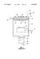
- Plasma process reactor 10includes a plasma chamber 12 in which is positioned a substrate holder 14. A semiconductor substrate 16 is placed on substrate holder 14. A bias voltage controller 18 is coupled to substrate holder 14 in order to bias the voltage to counter the charges building up on semiconductor substrate 16. An etching gas is provided through gas inlet 20, which is ionized by inductor backside 22. Placed upon inductor backside 22 is a plurality of inductor elements 24 that is controlled by a current 26. Current 26 causes an induction current to flow that generates an ionizing field on the interior surface of inductor backside 22.
- the plasmathen passes through a gas distribution plate 28, which is held in place with a vacuum seal via O-ring 30, allowing a gas to pass through a plurality of apertures 32.
- a second O-ring 34is placed between the inductor backside 22 and gas distribution plate 28.
- a vacuumis created by a vacuum pump 36 for evacuating material and pressure from plasma chamber 12.
- a control gate 38is provided to allow a more precise control of the vacuum, as well as the evacuated material.
- An outlet 40removes the material from the vacuum for disposal.
- gas distribution plate 28is made of a silicon nitride material. In certain desired oxide etch processes, it is required that the gas distribution plate 28 be cooled below 80° C. This cooling is accomplished by cooling the reactor wall of plasma chamber 12 and is sometimes called a window in this plasma etch reactor. The reactor wall is cooled to about 20° C. and the process gas is run through the backside gap. Unfortunately, the temperature of the inductor backside 22 cannot be easily modified in this arrangement. The inability to control the temperature causes other problems during different stages of use of the process reactor.
- a plasma process reactorthat allows for greater control in varying the functional temperature range for enhancing semiconductor processing and reactor cleaning.
- the temperatureis controlled by splitting the process gas flow from a single gas manifold that injects the process gas behind the gas distribution plate into two streams where the first stream goes behind the gas distribution plate and the second stream is injected directly into the chamber.
- the temperature of the gas distribution platecan be increased.
- the increasing of the chamber temperatureresults in higher O 2 plasma cleaning rates of the deposits on the hotter surfaces.
- the high gas flowallows higher temperatures to be achieved over the non-split flow of the prior art.
- FIG. 1is a schematic diagram of a plasma process reactor according to the prior art
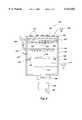
- FIG. 2is a schematic diagram of a plasma process reactor having a split fold plasma manifold and injector according to the present invention
- FIG. 3is a schematic diagram of a top plan view of a gas distribution ring providing the secondary gas flow into the chamber;
- FIG. 4is an alternative embodiment of the gas flow ring used in the plasma process reactor of FIG. 2.
- a high density, plasma process reactor 100is depicted in the schematic diagram of FIG. 2.
- the reactormay have multiple plasma sources where one source is for etching layers in a semiconductor substrate while the other source is for depositing a polymer.
- Reactor 100is a low pressure reactor that operates at or below 50 milliTorr. Low pressure reactors are desired, as they avoid microscopic loading, where features of the same size etch more slowly in dense patterns than in sparse patterns.
- the reactor 100has separate controls for top and bottom power. The top power is for energizing high density plasma sources and the bottom power or bias source is for directing the plasma for etching and for directing a polymer for depositing.
- the high density plasma process reactor 100is modeled after an LAM 9100 TCP (transferred coupled plasma) etcher and an Applied Materials HDP 5300.
- High density plasmais defined as plasma having an ion density greater than 1 ⁇ 10 10 per centimeter 3 in a plasma generation zone. Typically, high density plasmas range in ion density from 10 11 to 10 13 per cm 3 .
- Process reactor 100increases the range of process results capable of being obtained, as well as improves the ability to clean the chamber by adding a second process gas flow inlet that avoids gas passing through the gas distribution plate on the backside of the reactor.
- Reactor 100is similar in construction to that of the prior art reactor 10 in FIG. 1.
- Reactor 100includes a chamber 112 in which is placed a substrate support platform 114 that holds semiconductor substrate 116.
- a plurality of semiconductor substrates 116can be placed upon substrate support platform 114.
- the bottom bias sourceis controlled by voltage supply 118 that either grounds substrate support 114 or holds it at a selected voltage to attract the plasma generated within reactor 100.
- a first process gas inlet 120is provided that feeds process gas within a chamber formed by reactor backside 122 and gas distribution plate (or dielectric) 128.
- Gas distribution plate 128further includes a dielectric layer 129, placed on the backside 122 of gas distribution plate 128.
- a plurality of inductive power sources 124which is controlled by power supply 126, is mounted to the reactor backside 122 for inductively coupling energy to form the plasma that is emitted through apertures 132 in gas distribution plate 128.
- a first O-ring 130is used to seal gas distribution plate 128 in place within chamber 112 and a second O-ring 134 is used to form the chamber between reactor backside 122 and gas distribution plate 128.
- a vacuumis created by a vacuum pump 136 for evacuating material and pressure from plasma chamber 112.
- a control gate 138is provided to allow a more precise control of the vacuum, as well as the evacuated material.
- An outlet 140removes the material from the vacuum for disposal.
- Process reactor 100further includes a second process gas inlet 142 as well as an auxiliary oxygen inlet 144; both inlets provide gas flow into chamber 112 and thus bypass gas distribution plate 128.
- a second process gas inlet 142as well as an auxiliary oxygen inlet 144; both inlets provide gas flow into chamber 112 and thus bypass gas distribution plate 128.
- the fractional flowdecreases that flows behind the gas distribution plate 128, thus allowing the temperature of gas distribution plate 128 to increase.
- Inlets 120, 142, and 144can be controlled by a mechanical valve (not shown) that is electronically controlled to open and close at different times.
- the second process gas inlet 142actually feeds into a distribution ring 146.
- a pair of distribution rings 146, 148are placed within the reactor, one above semiconductor substrate 116 and another substantially coplanar to semiconductor substrate 116.
- distribution ring 146it is an annular ring with gas vents that point downwardly towards semiconductor distribution substrate 116.
- the ring 146is annular and thus provides a radial gas flow symmetrical to the semiconductor substrate 116.
- the alternative ring 148which may be used in tandem with the first ring, has jets 150 that direct the gas flow upward and radially inward for uniform distribution to semiconductor substrate 116.
- reactor 100uses the additional inlet valves to improve its cleaning ability, as well as provide process modifications.
- the process gasis 100% injected through the side, the cooling of the dielectric layer 129 on gas distribution plate 128 diminishes and the O 2 plasma can now clean deposits from the gas distribution plate 128, because it is thermally uncoupled from the rear reactor backside 122 during the cleaning step. Further, residue, such as fluorocarbon polymers, are quickly and more efficiently cleaned off of gas distribution plate 128 because of the higher temperature.
- the change in gas temperatureis inversely-proportional to the change in pressure within chamber 112. Accordingly, by reducing the pressure behind gas distribution plate 128, the temperature of the gas flow can increase by bypassing gas distribution plate 128.
- FIG. 3is a bottom plan view of a second inlet gas distribution ring 146.
- Distribution ring 146includes an annular gas vent 152 that has a plurality of holes 154 distributed around the inner perimeter. The holes can be directed to point either perpendicular to the plane of distribution ring 146 or to point slightly inwardly radially towards the axis of the annular gas vent 152.
- An inlet connector 156is provided to attach distribution ring 146 to the interior of chamber 112.
- FIG. 4depicts an alternative embodiment of the distribution ring 146. In this embodiment, distribution ring 146 has a square or polygonal shaped gas vent 158.
- a plurality of holes 154is provided along the bottom surface of gas vent 158.
- an inlet connector 156is provided to connect distribution ring 146 to the second process gas inlet 142 within chamber 112.
- Either ring of FIG. 3 or FIG. 4can be placed in the position of ring 146 in FIG. 2. Additionally, either ring can be placed in a position of distribution ring 148 having jets 150 that are substantially coplanar with the semiconductor substrate 116.
- T 12880° C.
- T 128110° C.
- Table IIprovides the values for when the flow is either 100% through inlet 120 or inlet 142:
- the chamber pressureis independent of the pressure behind dielectric plate 128.
- the pressure for 100% of the flow through second process gas inlet 120is dependent on O 2 flow rates shown in Table I.
- the present inventionmay be employed to fabricate a variety of devices such as, for example, memory devices. These other devices are not necessarily limited to memory devices but can include applications, specific integrated circuits, microprocessors, microcontroller, digital signal processor, and the like. Moreover, such devices may be employed in a variety of systems, such systems including, but not limited to, memory modules, network cards, telephones, scanners, facsimile machines, routers, copying machines, displays, printers, calculators, and computers, among others.
Landscapes
- Chemical & Material Sciences (AREA)
- Engineering & Computer Science (AREA)
- Physics & Mathematics (AREA)
- Chemical Kinetics & Catalysis (AREA)
- Materials Engineering (AREA)
- Mechanical Engineering (AREA)
- Metallurgy (AREA)
- Organic Chemistry (AREA)
- General Chemical & Material Sciences (AREA)
- Plasma & Fusion (AREA)
- Analytical Chemistry (AREA)
- Condensed Matter Physics & Semiconductors (AREA)
- General Physics & Mathematics (AREA)
- Manufacturing & Machinery (AREA)
- Computer Hardware Design (AREA)
- Microelectronics & Electronic Packaging (AREA)
- Power Engineering (AREA)
- Drying Of Semiconductors (AREA)
Abstract
Description
TABLE I ______________________________________ CHAMBER FLOWS PRESSURE AT DIELECTRIC PRESSURE GASES (sccm) PLATE 128 (Torr) (mTorr) ______________________________________ C.sub.2 HF.sub.5 15 30-40 5-50 N.sub.2 5 CHF.sub.3 15 CH.sub.2 F.sub.2 15 ______________________________________
TABLE II ______________________________________PRESSURE 100% throughInlet 120 100% throughInlet 142 BehindPlate 128 30-500 mTorr 5-500 mTorr In Chamber 5-500 mTorr 5-500 mTorr ______________________________________
Claims (42)
Priority Applications (10)
| Application Number | Priority Date | Filing Date | Title |
|---|---|---|---|
| US09/026,246US6132552A (en) | 1998-02-19 | 1998-02-19 | Method and apparatus for controlling the temperature of a gas distribution plate in a process reactor |
| US09/514,820US6323133B1 (en) | 1998-02-19 | 2000-02-28 | Method and apparatus for controlling the temperature of a gas distribution plate in a process reactor |
| US09/680,638US6299725B1 (en) | 1998-02-19 | 2000-10-06 | Method and apparatus for controlling the temperature of a gas distribution plate in a process reactor |
| US09/924,628US6383334B1 (en) | 1998-02-19 | 2001-08-08 | Method and apparatus for controlling the temperature of a gas distribution plate in a process reactor |
| US09/944,503US6387816B2 (en) | 1998-02-19 | 2001-08-30 | Method and apparatus for controlling the temperature of a gas distribution plate in a process reactor |
| US10/127,273US6617256B2 (en) | 1998-02-19 | 2002-04-22 | Method for controlling the temperature of a gas distribution plate in a process reactor |
| US10/127,104US6613189B2 (en) | 1998-02-19 | 2002-04-22 | Apparatus for controlling the temperature of a gas distribution plate in a process reactor |
| US10/651,424US6833049B2 (en) | 1998-02-19 | 2003-08-29 | Apparatus for controlling the temperature of a gas distribution plate in a process reactor |
| US10/651,423US6960534B2 (en) | 1998-02-19 | 2003-08-29 | Method for controlling the temperature of a gas distribution plate in a process reactor |
| US11/237,604US20060021969A1 (en) | 1998-02-19 | 2005-09-27 | Method for controlling the temperature of a gas distribution plate in a process reactor |
Applications Claiming Priority (1)
| Application Number | Priority Date | Filing Date | Title |
|---|---|---|---|
| US09/026,246US6132552A (en) | 1998-02-19 | 1998-02-19 | Method and apparatus for controlling the temperature of a gas distribution plate in a process reactor |
Related Child Applications (2)
| Application Number | Title | Priority Date | Filing Date |
|---|---|---|---|
| US09/514,820DivisionUS6323133B1 (en) | 1998-02-19 | 2000-02-28 | Method and apparatus for controlling the temperature of a gas distribution plate in a process reactor |
| US09/680,638ContinuationUS6299725B1 (en) | 1998-02-19 | 2000-10-06 | Method and apparatus for controlling the temperature of a gas distribution plate in a process reactor |
Publications (1)
| Publication Number | Publication Date |
|---|---|
| US6132552Atrue US6132552A (en) | 2000-10-17 |
Family
ID=21830708
Family Applications (10)
| Application Number | Title | Priority Date | Filing Date |
|---|---|---|---|
| US09/026,246Expired - LifetimeUS6132552A (en) | 1998-02-19 | 1998-02-19 | Method and apparatus for controlling the temperature of a gas distribution plate in a process reactor |
| US09/514,820Expired - Fee RelatedUS6323133B1 (en) | 1998-02-19 | 2000-02-28 | Method and apparatus for controlling the temperature of a gas distribution plate in a process reactor |
| US09/680,638Expired - Fee RelatedUS6299725B1 (en) | 1998-02-19 | 2000-10-06 | Method and apparatus for controlling the temperature of a gas distribution plate in a process reactor |
| US09/924,628Expired - Fee RelatedUS6383334B1 (en) | 1998-02-19 | 2001-08-08 | Method and apparatus for controlling the temperature of a gas distribution plate in a process reactor |
| US09/944,503Expired - Fee RelatedUS6387816B2 (en) | 1998-02-19 | 2001-08-30 | Method and apparatus for controlling the temperature of a gas distribution plate in a process reactor |
| US10/127,104Expired - Fee RelatedUS6613189B2 (en) | 1998-02-19 | 2002-04-22 | Apparatus for controlling the temperature of a gas distribution plate in a process reactor |
| US10/127,273Expired - Fee RelatedUS6617256B2 (en) | 1998-02-19 | 2002-04-22 | Method for controlling the temperature of a gas distribution plate in a process reactor |
| US10/651,423Expired - Fee RelatedUS6960534B2 (en) | 1998-02-19 | 2003-08-29 | Method for controlling the temperature of a gas distribution plate in a process reactor |
| US10/651,424Expired - Fee RelatedUS6833049B2 (en) | 1998-02-19 | 2003-08-29 | Apparatus for controlling the temperature of a gas distribution plate in a process reactor |
| US11/237,604AbandonedUS20060021969A1 (en) | 1998-02-19 | 2005-09-27 | Method for controlling the temperature of a gas distribution plate in a process reactor |
Family Applications After (9)
| Application Number | Title | Priority Date | Filing Date |
|---|---|---|---|
| US09/514,820Expired - Fee RelatedUS6323133B1 (en) | 1998-02-19 | 2000-02-28 | Method and apparatus for controlling the temperature of a gas distribution plate in a process reactor |
| US09/680,638Expired - Fee RelatedUS6299725B1 (en) | 1998-02-19 | 2000-10-06 | Method and apparatus for controlling the temperature of a gas distribution plate in a process reactor |
| US09/924,628Expired - Fee RelatedUS6383334B1 (en) | 1998-02-19 | 2001-08-08 | Method and apparatus for controlling the temperature of a gas distribution plate in a process reactor |
| US09/944,503Expired - Fee RelatedUS6387816B2 (en) | 1998-02-19 | 2001-08-30 | Method and apparatus for controlling the temperature of a gas distribution plate in a process reactor |
| US10/127,104Expired - Fee RelatedUS6613189B2 (en) | 1998-02-19 | 2002-04-22 | Apparatus for controlling the temperature of a gas distribution plate in a process reactor |
| US10/127,273Expired - Fee RelatedUS6617256B2 (en) | 1998-02-19 | 2002-04-22 | Method for controlling the temperature of a gas distribution plate in a process reactor |
| US10/651,423Expired - Fee RelatedUS6960534B2 (en) | 1998-02-19 | 2003-08-29 | Method for controlling the temperature of a gas distribution plate in a process reactor |
| US10/651,424Expired - Fee RelatedUS6833049B2 (en) | 1998-02-19 | 2003-08-29 | Apparatus for controlling the temperature of a gas distribution plate in a process reactor |
| US11/237,604AbandonedUS20060021969A1 (en) | 1998-02-19 | 2005-09-27 | Method for controlling the temperature of a gas distribution plate in a process reactor |
Country Status (1)
| Country | Link |
|---|---|
| US (10) | US6132552A (en) |
Cited By (74)
| Publication number | Priority date | Publication date | Assignee | Title |
|---|---|---|---|---|
| WO2001037317A1 (en)* | 1999-11-15 | 2001-05-25 | Lam Research Corporation | Plasma processing system with dynamic gas distribution control |
| US6299725B1 (en) | 1998-02-19 | 2001-10-09 | Micron Technology, Inc. | Method and apparatus for controlling the temperature of a gas distribution plate in a process reactor |
| US6417111B2 (en)* | 1999-07-05 | 2002-07-09 | Mitsubishi Denki Kabushiki Kaisha | Plasma processing apparatus |
| WO2002061179A1 (en)* | 2001-01-19 | 2002-08-08 | Tokyo Electron Limited | Method and apparatus for gas injection system with minimum particulate contamination |
| US20020129768A1 (en)* | 2001-03-15 | 2002-09-19 | Carpenter Craig M. | Chemical vapor deposition apparatuses and deposition methods |
| US6453842B1 (en)* | 2000-08-11 | 2002-09-24 | Applied Materials Inc. | Externally excited torroidal plasma source using a gas distribution plate |
| US6458723B1 (en) | 1999-06-24 | 2002-10-01 | Silicon Genesis Corporation | High temperature implant apparatus |
| US6474257B2 (en)* | 2001-02-20 | 2002-11-05 | Macronix International Co., Ltd. | High density plasma chemical vapor deposition chamber |
| US6494986B1 (en)* | 2000-08-11 | 2002-12-17 | Applied Materials, Inc. | Externally excited multiple torroidal plasma source |
| US20020192972A1 (en)* | 2001-03-29 | 2002-12-19 | Masaki Narita | Plasma processing |
| US6514838B2 (en) | 1998-02-17 | 2003-02-04 | Silicon Genesis Corporation | Method for non mass selected ion implant profile control |
| US20030047449A1 (en)* | 2000-08-11 | 2003-03-13 | Applied Materials, Inc. | Method to drive spatially separate resonant structure with spatially distinct plasma secondaries using a single generator and switching elements |
| US20030064169A1 (en)* | 2001-09-28 | 2003-04-03 | Hong Jin Pyo | Plasma enhanced chemical vapor deposition apparatus and method of producing carbon nanotube using the same |
| US20030073316A1 (en)* | 1998-12-07 | 2003-04-17 | Taiwan Semiconductor Manufacturing Company | Novel post etching treatment process for high density oxide etcher |
| US6551446B1 (en) | 2000-08-11 | 2003-04-22 | Applied Materials Inc. | Externally excited torroidal plasma source with a gas distribution plate |
| US20030168011A1 (en)* | 2000-05-02 | 2003-09-11 | Bong-Ju Lee | Apparatus for treating the surface wit neutral particle beams |
| US6632322B1 (en) | 2000-06-30 | 2003-10-14 | Lam Research Corporation | Switched uniformity control |
| US6641673B2 (en)* | 2000-12-20 | 2003-11-04 | General Electric Company | Fluid injector for and method of prolonged delivery and distribution of reagents into plasma |
| US20030226641A1 (en)* | 2000-08-11 | 2003-12-11 | Applied Materials, Inc. | Externally excited torroidal plasma source with magnetic control of ion distribution |
| US6676760B2 (en)* | 2001-08-16 | 2004-01-13 | Appiled Materials, Inc. | Process chamber having multiple gas distributors and method |
| US20040011464A1 (en)* | 2002-07-16 | 2004-01-22 | Applied Materials, Inc. | Promotion of independence between degree of dissociation of reactive gas and the amount of ionization of dilutant gas via diverse gas injection |
| US6689220B1 (en)* | 2000-11-22 | 2004-02-10 | Simplus Systems Corporation | Plasma enhanced pulsed layer deposition |
| US20040094092A1 (en)* | 2002-02-25 | 2004-05-20 | Derderian Garo J. | Apparatus for improved delivery of metastable species |
| US20040099216A1 (en)* | 2002-11-27 | 2004-05-27 | Seok-Keun Koh | Apparatus for modifying surface of material using ion beam |
| US20040135828A1 (en)* | 2003-01-15 | 2004-07-15 | Schmitt Stephen E. | Printer and method for printing an item with a high durability and/or resolution image |
| US20040144310A1 (en)* | 2001-08-17 | 2004-07-29 | Campbell Philip H. | CVD apparatuses and methods of forming a layer over a semiconductor substrate |
| US20040149218A1 (en)* | 2000-08-11 | 2004-08-05 | Applied Materials, Inc. | Plasma immersion ion implantation process using a capacitively coupled plasma source having low dissociation and low minimum plasma voltage |
| US20040194708A1 (en)* | 2001-01-22 | 2004-10-07 | Anelva Corporation | Method of cleaning a cvd device |
| US6835277B2 (en)* | 2001-06-16 | 2004-12-28 | Samsung Electronics Co., Ltd. | Ashing apparatus for semiconductor device |
| US20050093460A1 (en)* | 2003-11-04 | 2005-05-05 | Samsung Electronics Co., Ltd. | Helical resonator type plasma processing apparatus |
| US6893907B2 (en) | 2002-06-05 | 2005-05-17 | Applied Materials, Inc. | Fabrication of silicon-on-insulator structure using plasma immersion ion implantation |
| US20050109279A1 (en)* | 2003-11-07 | 2005-05-26 | Shimadzu Corporation | Surface wave excitation plasma CVD system |
| US20050160982A1 (en)* | 2004-01-27 | 2005-07-28 | Ha Min-No | Plasma enhanced semicondutor deposition apparatus |
| US20050191416A1 (en)* | 2002-08-15 | 2005-09-01 | Cem Basceri | Methods of gas delivery for deposition processes and methods of depositing material on a substrate |
| US20050194475A1 (en)* | 2004-03-04 | 2005-09-08 | Han-Ki Kim | Inductively coupled plasma chemical vapor deposition apparatus |
| US20050224181A1 (en)* | 2004-04-08 | 2005-10-13 | Applied Materials, Inc. | Method and apparatus for in-situ film stack processing |
| US20060003237A1 (en)* | 2003-09-12 | 2006-01-05 | Micron Technology, Inc. | Transparent amorphous carbon structure in semiconductor devices |
| US20060011583A1 (en)* | 1999-11-15 | 2006-01-19 | Bailey Andrew D Iii | Materials and gas chemistries for processing systems |
| US20060021574A1 (en)* | 2004-08-02 | 2006-02-02 | Veeco Instruments Inc. | Multi-gas distribution injector for chemical vapor deposition reactors |
| US20060121193A1 (en)* | 2003-04-30 | 2006-06-08 | Strauch Gerhard K | Process and apparatus for depositing semiconductor layers using two process gases, one of which is preconditioned |
| US7094670B2 (en) | 2000-08-11 | 2006-08-22 | Applied Materials, Inc. | Plasma immersion ion implantation process |
| US7094316B1 (en) | 2000-08-11 | 2006-08-22 | Applied Materials, Inc. | Externally excited torroidal plasma source |
| US7109098B1 (en) | 2005-05-17 | 2006-09-19 | Applied Materials, Inc. | Semiconductor junction formation process including low temperature plasma deposition of an optical absorption layer and high speed optical annealing |
| US7137354B2 (en) | 2000-08-11 | 2006-11-21 | Applied Materials, Inc. | Plasma immersion ion implantation apparatus including a plasma source having low dissociation and low minimum plasma voltage |
| US7166524B2 (en) | 2000-08-11 | 2007-01-23 | Applied Materials, Inc. | Method for ion implanting insulator material to reduce dielectric constant |
| US7183177B2 (en) | 2000-08-11 | 2007-02-27 | Applied Materials, Inc. | Silicon-on-insulator wafer transfer method using surface activation plasma immersion ion implantation for wafer-to-wafer adhesion enhancement |
| US7223676B2 (en) | 2002-06-05 | 2007-05-29 | Applied Materials, Inc. | Very low temperature CVD process with independently variable conformality, stress and composition of the CVD layer |
| US7244474B2 (en) | 2004-03-26 | 2007-07-17 | Applied Materials, Inc. | Chemical vapor deposition plasma process using an ion shower grid |
| US7288491B2 (en) | 2000-08-11 | 2007-10-30 | Applied Materials, Inc. | Plasma immersion ion implantation process |
| US7291360B2 (en) | 2004-03-26 | 2007-11-06 | Applied Materials, Inc. | Chemical vapor deposition plasma process using plural ion shower grids |
| US7294563B2 (en) | 2000-08-10 | 2007-11-13 | Applied Materials, Inc. | Semiconductor on insulator vertical transistor fabrication and doping process |
| US7303982B2 (en) | 2000-08-11 | 2007-12-04 | Applied Materials, Inc. | Plasma immersion ion implantation process using an inductively coupled plasma source having low dissociation and low minimum plasma voltage |
| US7312162B2 (en) | 2005-05-17 | 2007-12-25 | Applied Materials, Inc. | Low temperature plasma deposition process for carbon layer deposition |
| US7312148B2 (en) | 2005-08-08 | 2007-12-25 | Applied Materials, Inc. | Copper barrier reflow process employing high speed optical annealing |
| US7320734B2 (en) | 2000-08-11 | 2008-01-22 | Applied Materials, Inc. | Plasma immersion ion implantation system including a plasma source having low dissociation and low minimum plasma voltage |
| US7323401B2 (en) | 2005-08-08 | 2008-01-29 | Applied Materials, Inc. | Semiconductor substrate process using a low temperature deposited carbon-containing hard mask |
| US7335611B2 (en) | 2005-08-08 | 2008-02-26 | Applied Materials, Inc. | Copper conductor annealing process employing high speed optical annealing with a low temperature-deposited optical absorber layer |
| US7422775B2 (en) | 2005-05-17 | 2008-09-09 | Applied Materials, Inc. | Process for low temperature plasma deposition of an optical absorption layer and high speed optical annealing |
| US7428915B2 (en) | 2005-04-26 | 2008-09-30 | Applied Materials, Inc. | O-ringless tandem throttle valve for a plasma reactor chamber |
| US7429532B2 (en) | 2005-08-08 | 2008-09-30 | Applied Materials, Inc. | Semiconductor substrate process using an optically writable carbon-containing mask |
| US20080289576A1 (en)* | 2007-05-23 | 2008-11-27 | Samsung Electronics Co., Ltd. | Plasma based ion implantation system |
| US7465478B2 (en) | 2000-08-11 | 2008-12-16 | Applied Materials, Inc. | Plasma immersion ion implantation process |
| US7479456B2 (en) | 2004-08-26 | 2009-01-20 | Applied Materials, Inc. | Gasless high voltage high contact force wafer contact-cooling electrostatic chuck |
| US7666464B2 (en) | 2004-10-23 | 2010-02-23 | Applied Materials, Inc. | RF measurement feedback control and diagnostics for a plasma immersion ion implantation reactor |
| US7695590B2 (en) | 2004-03-26 | 2010-04-13 | Applied Materials, Inc. | Chemical vapor deposition plasma reactor having plural ion shower grids |
| US7767561B2 (en) | 2004-07-20 | 2010-08-03 | Applied Materials, Inc. | Plasma immersion ion implantation reactor having an ion shower grid |
| US20110180213A1 (en)* | 2008-06-11 | 2011-07-28 | Tokyo Electron Limited | Plasma processing apparatus and plasma processing method |
| US8058156B2 (en) | 2004-07-20 | 2011-11-15 | Applied Materials, Inc. | Plasma immersion ion implantation reactor having multiple ion shower grids |
| US20120037077A1 (en)* | 2002-05-03 | 2012-02-16 | Giacomo Benvenuti | Large area deposition in high vacuum with high thickness uniformity |
| US20130098293A1 (en)* | 2011-10-20 | 2013-04-25 | Samsung Electronics Co., Ltd. | Chemical vapor deposition apparatus |
| US10208380B2 (en)* | 2015-12-04 | 2019-02-19 | Applied Materials, Inc. | Advanced coating method and materials to prevent HDP-CVD chamber arcing |
| CN114068272A (en)* | 2020-07-31 | 2022-02-18 | 中微半导体设备(上海)股份有限公司 | Gas flow regulating device and regulating method and plasma processing device |
| US11264218B2 (en)* | 2019-02-01 | 2022-03-01 | Tokyo Electron Limited | Substrate processing apparatus and cleaning method |
| US11769652B2 (en)* | 2018-07-31 | 2023-09-26 | Taiwan Semiconductor Manufacturing Co., Ltd. | Devices and methods for controlling wafer uniformity in plasma-based process |
Families Citing this family (21)
| Publication number | Priority date | Publication date | Assignee | Title |
|---|---|---|---|---|
| EP1308992A4 (en)* | 2000-08-11 | 2006-01-18 | Tokyo Electron Ltd | Device and method for processing substrate |
| CN101038863B (en)* | 2001-02-15 | 2011-07-06 | 东京毅力科创株式会社 | Method and apparatus for processing workpiece |
| US7141138B2 (en)* | 2002-09-13 | 2006-11-28 | Applied Materials, Inc. | Gas delivery system for semiconductor processing |
| US20040261946A1 (en)* | 2003-04-24 | 2004-12-30 | Tokyo Electron Limited | Plasma processing apparatus, focus ring, and susceptor |
| TW200537695A (en)* | 2004-03-19 | 2005-11-16 | Adv Lcd Tech Dev Ct Co Ltd | Insulating film forming method, insulating film forming apparatus, and plasma film forming apparatus |
| US20060062914A1 (en)* | 2004-09-21 | 2006-03-23 | Diwakar Garg | Apparatus and process for surface treatment of substrate using an activated reactive gas |
| JP4854317B2 (en)* | 2006-01-31 | 2012-01-18 | 東京エレクトロン株式会社 | Substrate processing method |
| EP1840936A1 (en)* | 2006-03-29 | 2007-10-03 | Applied Materials GmbH & Co. KG | Sputtering chamber for coating a substrate |
| US20070264443A1 (en)* | 2006-05-09 | 2007-11-15 | Applied Materials, Inc. | Apparatus and method for avoidance of parasitic plasma in plasma source gas supply conduits |
| US20080083701A1 (en)* | 2006-10-04 | 2008-04-10 | Mks Instruments, Inc. | Oxygen conditioning of plasma vessels |
| KR100974566B1 (en) | 2008-08-08 | 2010-08-06 | 한국생산기술연구원 | Atmospheric pressure plasma device |
| KR101037188B1 (en) | 2008-12-17 | 2011-05-26 | 세메스 주식회사 | Plasma processing equipment |
| JP2010192513A (en)* | 2009-02-16 | 2010-09-02 | Hitachi High-Technologies Corp | Plasma processing apparatus and method of operating the same |
| WO2011021539A1 (en)* | 2009-08-20 | 2011-02-24 | 東京エレクトロン株式会社 | Plasma treatment device and plasma treatment method |
| JP5045786B2 (en)* | 2010-05-26 | 2012-10-10 | 東京エレクトロン株式会社 | Plasma processing equipment |
| US9499905B2 (en)* | 2011-07-22 | 2016-11-22 | Applied Materials, Inc. | Methods and apparatus for the deposition of materials on a substrate |
| JP6406811B2 (en)* | 2013-11-20 | 2018-10-17 | 国立大学法人名古屋大学 | III-nitride semiconductor device manufacturing apparatus and method, and semiconductor wafer manufacturing method |
| US9741575B2 (en)* | 2014-03-10 | 2017-08-22 | Taiwan Semiconductor Manufacturing Co., Ltd. | CVD apparatus with gas delivery ring |
| CN107073157B (en) | 2014-08-15 | 2021-03-02 | 约翰逊父子公司 | Wax furnace |
| KR102696320B1 (en)* | 2015-06-12 | 2024-08-20 | 어플라이드 머티어리얼스, 인코포레이티드 | Injector for semiconductor epitaxy growth |
| US20190051495A1 (en)* | 2017-08-10 | 2019-02-14 | Qiwei Liang | Microwave Reactor For Deposition or Treatment of Carbon Compounds |
Citations (6)
| Publication number | Priority date | Publication date | Assignee | Title |
|---|---|---|---|---|
| US4348577A (en)* | 1979-12-12 | 1982-09-07 | Vlsi Technology Research Association | High selectivity plasma etching method |
| US5500076A (en)* | 1993-06-22 | 1996-03-19 | Lsi Logic Corporation | Process for dynamic control of the concentration of one or more etchants in a plasma-enhanced etch process for formation of patterned layers of conductive material on integrated circuit structures |
| US5576629A (en)* | 1994-10-24 | 1996-11-19 | Fourth State Technology, Inc. | Plasma monitoring and control method and system |
| US5597439A (en)* | 1994-10-26 | 1997-01-28 | Applied Materials, Inc. | Process gas inlet and distribution passages |
| US5620523A (en)* | 1994-04-11 | 1997-04-15 | Canon Sales Co., Inc. | Apparatus for forming film |
| US5792261A (en)* | 1993-12-17 | 1998-08-11 | Tokyo Electron Limited | Plasma process apparatus |
Family Cites Families (13)
| Publication number | Priority date | Publication date | Assignee | Title |
|---|---|---|---|---|
| JPS61112513A (en)* | 1984-11-05 | 1986-05-30 | 中国化工株式会社 | How to repair pull boxes |
| JPS61125133A (en) | 1984-11-22 | 1986-06-12 | Hitachi Ltd | Low temperature plasma electromagnetic field control structure |
| JPS634081A (en)* | 1986-06-21 | 1988-01-09 | Nissin Electric Co Ltd | Etching device |
| DE3830249A1 (en)* | 1988-09-06 | 1990-03-15 | Schott Glaswerke | PLASMA PROCESS FOR COATING LEVEL SUBSTRATES |
| JPH04192328A (en)* | 1990-11-26 | 1992-07-10 | Toshiba Corp | plasma processing equipment |
| US20010054601A1 (en)* | 1996-05-13 | 2001-12-27 | Jian Ding | Low ceiling temperature process for a plasma reactor with heated source of a polymer-hardening precursor material |
| US5522934A (en)* | 1994-04-26 | 1996-06-04 | Tokyo Electron Limited | Plasma processing apparatus using vertical gas inlets one on top of another |
| US5576626A (en) | 1995-01-17 | 1996-11-19 | Microsensor Technology, Inc. | Compact and low fuel consumption flame ionization detector with flame tip on diffuser |
| JP3317209B2 (en)* | 1997-08-12 | 2002-08-26 | 東京エレクトロンエイ・ティー株式会社 | Plasma processing apparatus and plasma processing method |
| US6132552A (en) | 1998-02-19 | 2000-10-17 | Micron Technology, Inc. | Method and apparatus for controlling the temperature of a gas distribution plate in a process reactor |
| JP2000100742A (en)* | 1998-09-25 | 2000-04-07 | Dainippon Screen Mfg Co Ltd | Heat treatment equipment |
| US6263249B1 (en)* | 1999-02-26 | 2001-07-17 | Medtronic, Inc. | Medical electrical lead having controlled texture surface and method of making same |
| US7296532B2 (en)* | 2002-12-18 | 2007-11-20 | Taiwan Semiconductor Manufacturing Co., Ltd. | Bypass gas feed system and method to improve reactant gas flow and film deposition |
- 1998
- 1998-02-19USUS09/026,246patent/US6132552A/ennot_activeExpired - Lifetime
- 2000
- 2000-02-28USUS09/514,820patent/US6323133B1/ennot_activeExpired - Fee Related
- 2000-10-06USUS09/680,638patent/US6299725B1/ennot_activeExpired - Fee Related
- 2001
- 2001-08-08USUS09/924,628patent/US6383334B1/ennot_activeExpired - Fee Related
- 2001-08-30USUS09/944,503patent/US6387816B2/ennot_activeExpired - Fee Related
- 2002
- 2002-04-22USUS10/127,104patent/US6613189B2/ennot_activeExpired - Fee Related
- 2002-04-22USUS10/127,273patent/US6617256B2/ennot_activeExpired - Fee Related
- 2003
- 2003-08-29USUS10/651,423patent/US6960534B2/ennot_activeExpired - Fee Related
- 2003-08-29USUS10/651,424patent/US6833049B2/ennot_activeExpired - Fee Related
- 2005
- 2005-09-27USUS11/237,604patent/US20060021969A1/ennot_activeAbandoned
Patent Citations (6)
| Publication number | Priority date | Publication date | Assignee | Title |
|---|---|---|---|---|
| US4348577A (en)* | 1979-12-12 | 1982-09-07 | Vlsi Technology Research Association | High selectivity plasma etching method |
| US5500076A (en)* | 1993-06-22 | 1996-03-19 | Lsi Logic Corporation | Process for dynamic control of the concentration of one or more etchants in a plasma-enhanced etch process for formation of patterned layers of conductive material on integrated circuit structures |
| US5792261A (en)* | 1993-12-17 | 1998-08-11 | Tokyo Electron Limited | Plasma process apparatus |
| US5620523A (en)* | 1994-04-11 | 1997-04-15 | Canon Sales Co., Inc. | Apparatus for forming film |
| US5576629A (en)* | 1994-10-24 | 1996-11-19 | Fourth State Technology, Inc. | Plasma monitoring and control method and system |
| US5597439A (en)* | 1994-10-26 | 1997-01-28 | Applied Materials, Inc. | Process gas inlet and distribution passages |
Cited By (120)
| Publication number | Priority date | Publication date | Assignee | Title |
|---|---|---|---|---|
| US6514838B2 (en) | 1998-02-17 | 2003-02-04 | Silicon Genesis Corporation | Method for non mass selected ion implant profile control |
| US6960534B2 (en) | 1998-02-19 | 2005-11-01 | Micron Technology, Inc. | Method for controlling the temperature of a gas distribution plate in a process reactor |
| US6299725B1 (en) | 1998-02-19 | 2001-10-09 | Micron Technology, Inc. | Method and apparatus for controlling the temperature of a gas distribution plate in a process reactor |
| US6383334B1 (en) | 1998-02-19 | 2002-05-07 | Micron Technology, Inc. | Method and apparatus for controlling the temperature of a gas distribution plate in a process reactor |
| US6387816B2 (en) | 1998-02-19 | 2002-05-14 | Micron Technology, Inc. | Method and apparatus for controlling the temperature of a gas distribution plate in a process reactor |
| US20040038551A1 (en)* | 1998-02-19 | 2004-02-26 | Donohoe Kevin G. | Method for controlling the temperature of a gas distribution plate in a process reactor |
| US6617256B2 (en) | 1998-02-19 | 2003-09-09 | Micron Technology, Inc. | Method for controlling the temperature of a gas distribution plate in a process reactor |
| US6613189B2 (en) | 1998-02-19 | 2003-09-02 | Micron Technology, Inc. | Apparatus for controlling the temperature of a gas distribution plate in a process reactor |
| US20040035531A1 (en)* | 1998-02-19 | 2004-02-26 | Donohoe Kevin G. | Apparatus for controlling the temperature of a gas distribution plate in a process reactor |
| US6833049B2 (en) | 1998-02-19 | 2004-12-21 | Micron Technology, Inc. | Apparatus for controlling the temperature of a gas distribution plate in a process reactor |
| US20060021969A1 (en)* | 1998-02-19 | 2006-02-02 | Donohoe Kevin G | Method for controlling the temperature of a gas distribution plate in a process reactor |
| US20030089382A1 (en)* | 1998-12-07 | 2003-05-15 | Taiwan Semiconductor Manufacturing Company | Novel post etching treatment process for high density oxide etcher |
| US6889697B2 (en)* | 1998-12-07 | 2005-05-10 | Taiwan Semiconductor Manufacturing Company, Ltd. | Post etching treatment process for high density oxide etcher |
| US20030073316A1 (en)* | 1998-12-07 | 2003-04-17 | Taiwan Semiconductor Manufacturing Company | Novel post etching treatment process for high density oxide etcher |
| US6458723B1 (en) | 1999-06-24 | 2002-10-01 | Silicon Genesis Corporation | High temperature implant apparatus |
| US6417111B2 (en)* | 1999-07-05 | 2002-07-09 | Mitsubishi Denki Kabushiki Kaisha | Plasma processing apparatus |
| US20060011583A1 (en)* | 1999-11-15 | 2006-01-19 | Bailey Andrew D Iii | Materials and gas chemistries for processing systems |
| WO2001037317A1 (en)* | 1999-11-15 | 2001-05-25 | Lam Research Corporation | Plasma processing system with dynamic gas distribution control |
| US6935269B2 (en)* | 2000-05-02 | 2005-08-30 | Sem Technology Co., Ltd. | Apparatus for treating the surface with neutral particle beams |
| US20030168011A1 (en)* | 2000-05-02 | 2003-09-11 | Bong-Ju Lee | Apparatus for treating the surface wit neutral particle beams |
| US20040031564A1 (en)* | 2000-06-30 | 2004-02-19 | Lam Research Corporation | Switched uniformity control |
| US7282454B2 (en) | 2000-06-30 | 2007-10-16 | Lam Research Corporation | Switched uniformity control |
| US6632322B1 (en) | 2000-06-30 | 2003-10-14 | Lam Research Corporation | Switched uniformity control |
| US7294563B2 (en) | 2000-08-10 | 2007-11-13 | Applied Materials, Inc. | Semiconductor on insulator vertical transistor fabrication and doping process |
| US7037813B2 (en) | 2000-08-11 | 2006-05-02 | Applied Materials, Inc. | Plasma immersion ion implantation process using a capacitively coupled plasma source having low dissociation and low minimum plasma voltage |
| US7430984B2 (en) | 2000-08-11 | 2008-10-07 | Applied Materials, Inc. | Method to drive spatially separate resonant structure with spatially distinct plasma secondaries using a single generator and switching elements |
| US7094316B1 (en) | 2000-08-11 | 2006-08-22 | Applied Materials, Inc. | Externally excited torroidal plasma source |
| US7094670B2 (en) | 2000-08-11 | 2006-08-22 | Applied Materials, Inc. | Plasma immersion ion implantation process |
| US20030226641A1 (en)* | 2000-08-11 | 2003-12-11 | Applied Materials, Inc. | Externally excited torroidal plasma source with magnetic control of ion distribution |
| US7166524B2 (en) | 2000-08-11 | 2007-01-23 | Applied Materials, Inc. | Method for ion implanting insulator material to reduce dielectric constant |
| US6551446B1 (en) | 2000-08-11 | 2003-04-22 | Applied Materials Inc. | Externally excited torroidal plasma source with a gas distribution plate |
| US7183177B2 (en) | 2000-08-11 | 2007-02-27 | Applied Materials, Inc. | Silicon-on-insulator wafer transfer method using surface activation plasma immersion ion implantation for wafer-to-wafer adhesion enhancement |
| US6453842B1 (en)* | 2000-08-11 | 2002-09-24 | Applied Materials Inc. | Externally excited torroidal plasma source using a gas distribution plate |
| US6494986B1 (en)* | 2000-08-11 | 2002-12-17 | Applied Materials, Inc. | Externally excited multiple torroidal plasma source |
| US7465478B2 (en) | 2000-08-11 | 2008-12-16 | Applied Materials, Inc. | Plasma immersion ion implantation process |
| US7137354B2 (en) | 2000-08-11 | 2006-11-21 | Applied Materials, Inc. | Plasma immersion ion implantation apparatus including a plasma source having low dissociation and low minimum plasma voltage |
| US7288491B2 (en) | 2000-08-11 | 2007-10-30 | Applied Materials, Inc. | Plasma immersion ion implantation process |
| US20040149218A1 (en)* | 2000-08-11 | 2004-08-05 | Applied Materials, Inc. | Plasma immersion ion implantation process using a capacitively coupled plasma source having low dissociation and low minimum plasma voltage |
| US7291545B2 (en) | 2000-08-11 | 2007-11-06 | Applied Materials, Inc. | Plasma immersion ion implantation process using a capacitively couple plasma source having low dissociation and low minimum plasma voltage |
| US6939434B2 (en) | 2000-08-11 | 2005-09-06 | Applied Materials, Inc. | Externally excited torroidal plasma source with magnetic control of ion distribution |
| US7303982B2 (en) | 2000-08-11 | 2007-12-04 | Applied Materials, Inc. | Plasma immersion ion implantation process using an inductively coupled plasma source having low dissociation and low minimum plasma voltage |
| US20030047449A1 (en)* | 2000-08-11 | 2003-03-13 | Applied Materials, Inc. | Method to drive spatially separate resonant structure with spatially distinct plasma secondaries using a single generator and switching elements |
| US7320734B2 (en) | 2000-08-11 | 2008-01-22 | Applied Materials, Inc. | Plasma immersion ion implantation system including a plasma source having low dissociation and low minimum plasma voltage |
| US20040137167A1 (en)* | 2000-11-22 | 2004-07-15 | Tue Nguyen | Plasma enhanced pulsed layer deposition |
| US7361387B2 (en) | 2000-11-22 | 2008-04-22 | Tegal Corporation | Plasma enhanced pulsed layer deposition |
| US6689220B1 (en)* | 2000-11-22 | 2004-02-10 | Simplus Systems Corporation | Plasma enhanced pulsed layer deposition |
| US20050005855A1 (en)* | 2000-11-22 | 2005-01-13 | Tegal Corporation | Plasma enhanced pulsed layer deposition |
| US6641673B2 (en)* | 2000-12-20 | 2003-11-04 | General Electric Company | Fluid injector for and method of prolonged delivery and distribution of reagents into plasma |
| US7563328B2 (en) | 2001-01-19 | 2009-07-21 | Tokyo Electron Limited | Method and apparatus for gas injection system with minimum particulate contamination |
| US20040079484A1 (en)* | 2001-01-19 | 2004-04-29 | Strang Eric J. | Method and apparatus for gas injection system with minimum particulate contamination |
| WO2002061179A1 (en)* | 2001-01-19 | 2002-08-08 | Tokyo Electron Limited | Method and apparatus for gas injection system with minimum particulate contamination |
| US20080276957A1 (en)* | 2001-01-22 | 2008-11-13 | Anelva Corporation | Method of cleaning a cvd device |
| US8105440B2 (en) | 2001-01-22 | 2012-01-31 | Canon Anelva Corporation | Method of cleaning a CVD device |
| US20040194708A1 (en)* | 2001-01-22 | 2004-10-07 | Anelva Corporation | Method of cleaning a cvd device |
| US6474257B2 (en)* | 2001-02-20 | 2002-11-05 | Macronix International Co., Ltd. | High density plasma chemical vapor deposition chamber |
| US20050241581A1 (en)* | 2001-03-15 | 2005-11-03 | Carpenter Craig M | Chemical vapor deposition apparatuses and deposition methods |
| US20020129768A1 (en)* | 2001-03-15 | 2002-09-19 | Carpenter Craig M. | Chemical vapor deposition apparatuses and deposition methods |
| US20020192972A1 (en)* | 2001-03-29 | 2002-12-19 | Masaki Narita | Plasma processing |
| US6835277B2 (en)* | 2001-06-16 | 2004-12-28 | Samsung Electronics Co., Ltd. | Ashing apparatus for semiconductor device |
| US6676760B2 (en)* | 2001-08-16 | 2004-01-13 | Appiled Materials, Inc. | Process chamber having multiple gas distributors and method |
| US20040144310A1 (en)* | 2001-08-17 | 2004-07-29 | Campbell Philip H. | CVD apparatuses and methods of forming a layer over a semiconductor substrate |
| US6849133B2 (en)* | 2001-08-17 | 2005-02-01 | Micron Technology, Inc. | CVD apparatuses and methods of forming a layer over a semiconductor substrate |
| US20050112890A1 (en)* | 2001-08-17 | 2005-05-26 | Campbell Philip H. | CVD apparatuses and methods of forming a layer over a semiconductor substrate |
| US20030064169A1 (en)* | 2001-09-28 | 2003-04-03 | Hong Jin Pyo | Plasma enhanced chemical vapor deposition apparatus and method of producing carbon nanotube using the same |
| GB2380494A (en)* | 2001-09-28 | 2003-04-09 | Hanyang Hak Won Co Ltd | Plasma enhanced chemical vapour deposition apparatus; producing carbon nanotubes |
| US7527693B2 (en) | 2002-02-25 | 2009-05-05 | Micron Technology, Inc. | Apparatus for improved delivery of metastable species |
| US20040094092A1 (en)* | 2002-02-25 | 2004-05-20 | Derderian Garo J. | Apparatus for improved delivery of metastable species |
| US7393562B2 (en) | 2002-02-25 | 2008-07-01 | Micron Technology, Inc. | Deposition methods for improved delivery of metastable species |
| US20120037077A1 (en)* | 2002-05-03 | 2012-02-16 | Giacomo Benvenuti | Large area deposition in high vacuum with high thickness uniformity |
| US8852344B2 (en)* | 2002-05-03 | 2014-10-07 | Ecole Polytechnique Federale De Lausanne (Epfl) | Large area deposition in high vacuum with high thickness uniformity |
| US7223676B2 (en) | 2002-06-05 | 2007-05-29 | Applied Materials, Inc. | Very low temperature CVD process with independently variable conformality, stress and composition of the CVD layer |
| US7700465B2 (en) | 2002-06-05 | 2010-04-20 | Applied Materials, Inc. | Plasma immersion ion implantation process using a plasma source having low dissociation and low minimum plasma voltage |
| US6893907B2 (en) | 2002-06-05 | 2005-05-17 | Applied Materials, Inc. | Fabrication of silicon-on-insulator structure using plasma immersion ion implantation |
| US7393765B2 (en) | 2002-06-05 | 2008-07-01 | Applied Materials, Inc. | Low temperature CVD process with selected stress of the CVD layer on CMOS devices |
| US20040011464A1 (en)* | 2002-07-16 | 2004-01-22 | Applied Materials, Inc. | Promotion of independence between degree of dissociation of reactive gas and the amount of ionization of dilutant gas via diverse gas injection |
| US7399499B2 (en) | 2002-08-15 | 2008-07-15 | Micron Technology, Inc. | Methods of gas delivery for deposition processes and methods of depositing material on a substrate |
| US20050191416A1 (en)* | 2002-08-15 | 2005-09-01 | Cem Basceri | Methods of gas delivery for deposition processes and methods of depositing material on a substrate |
| US20040099216A1 (en)* | 2002-11-27 | 2004-05-27 | Seok-Keun Koh | Apparatus for modifying surface of material using ion beam |
| US7819058B2 (en)* | 2003-01-15 | 2010-10-26 | Schmitt Stephen E | Printer for printing individuated items with high durability and/or resolution image |
| US20060102035A1 (en)* | 2003-01-15 | 2006-05-18 | Schmitt Stephen E | Printed item |
| US20040135828A1 (en)* | 2003-01-15 | 2004-07-15 | Schmitt Stephen E. | Printer and method for printing an item with a high durability and/or resolution image |
| US20100012034A1 (en)* | 2003-04-30 | 2010-01-21 | Gerhard Karl Strauch | Process And Apparatus For Depositing Semiconductor Layers Using Two Process Gases, One Of Which is Preconditioned |
| US20060121193A1 (en)* | 2003-04-30 | 2006-06-08 | Strauch Gerhard K | Process and apparatus for depositing semiconductor layers using two process gases, one of which is preconditioned |
| US7709398B2 (en)* | 2003-04-30 | 2010-05-04 | Aixtron Ag | Process and apparatus for depositing semiconductor layers using two process gases, one of which is preconditioned |
| US20060003237A1 (en)* | 2003-09-12 | 2006-01-05 | Micron Technology, Inc. | Transparent amorphous carbon structure in semiconductor devices |
| US20050093460A1 (en)* | 2003-11-04 | 2005-05-05 | Samsung Electronics Co., Ltd. | Helical resonator type plasma processing apparatus |
| US20050109279A1 (en)* | 2003-11-07 | 2005-05-26 | Shimadzu Corporation | Surface wave excitation plasma CVD system |
| US8307781B2 (en)* | 2003-11-07 | 2012-11-13 | Shimadzu Corporation | Surface wave excitation plasma CVD system |
| US20050160982A1 (en)* | 2004-01-27 | 2005-07-28 | Ha Min-No | Plasma enhanced semicondutor deposition apparatus |
| US20050194475A1 (en)* | 2004-03-04 | 2005-09-08 | Han-Ki Kim | Inductively coupled plasma chemical vapor deposition apparatus |
| US7291360B2 (en) | 2004-03-26 | 2007-11-06 | Applied Materials, Inc. | Chemical vapor deposition plasma process using plural ion shower grids |
| US7244474B2 (en) | 2004-03-26 | 2007-07-17 | Applied Materials, Inc. | Chemical vapor deposition plasma process using an ion shower grid |
| US7695590B2 (en) | 2004-03-26 | 2010-04-13 | Applied Materials, Inc. | Chemical vapor deposition plasma reactor having plural ion shower grids |
| US20050224181A1 (en)* | 2004-04-08 | 2005-10-13 | Applied Materials, Inc. | Method and apparatus for in-situ film stack processing |
| US7358192B2 (en) | 2004-04-08 | 2008-04-15 | Applied Materials, Inc. | Method and apparatus for in-situ film stack processing |
| US7767561B2 (en) | 2004-07-20 | 2010-08-03 | Applied Materials, Inc. | Plasma immersion ion implantation reactor having an ion shower grid |
| US8058156B2 (en) | 2004-07-20 | 2011-11-15 | Applied Materials, Inc. | Plasma immersion ion implantation reactor having multiple ion shower grids |
| US20100300359A1 (en)* | 2004-08-02 | 2010-12-02 | Veeco Instruments Inc. | Multi-gas distribution injector for chemical vapor deposition reactors |
| US20060021574A1 (en)* | 2004-08-02 | 2006-02-02 | Veeco Instruments Inc. | Multi-gas distribution injector for chemical vapor deposition reactors |
| US7479456B2 (en) | 2004-08-26 | 2009-01-20 | Applied Materials, Inc. | Gasless high voltage high contact force wafer contact-cooling electrostatic chuck |
| US7666464B2 (en) | 2004-10-23 | 2010-02-23 | Applied Materials, Inc. | RF measurement feedback control and diagnostics for a plasma immersion ion implantation reactor |
| US7428915B2 (en) | 2005-04-26 | 2008-09-30 | Applied Materials, Inc. | O-ringless tandem throttle valve for a plasma reactor chamber |
| US7312162B2 (en) | 2005-05-17 | 2007-12-25 | Applied Materials, Inc. | Low temperature plasma deposition process for carbon layer deposition |
| US7422775B2 (en) | 2005-05-17 | 2008-09-09 | Applied Materials, Inc. | Process for low temperature plasma deposition of an optical absorption layer and high speed optical annealing |
| US7109098B1 (en) | 2005-05-17 | 2006-09-19 | Applied Materials, Inc. | Semiconductor junction formation process including low temperature plasma deposition of an optical absorption layer and high speed optical annealing |
| US7312148B2 (en) | 2005-08-08 | 2007-12-25 | Applied Materials, Inc. | Copper barrier reflow process employing high speed optical annealing |
| US7323401B2 (en) | 2005-08-08 | 2008-01-29 | Applied Materials, Inc. | Semiconductor substrate process using a low temperature deposited carbon-containing hard mask |
| US7335611B2 (en) | 2005-08-08 | 2008-02-26 | Applied Materials, Inc. | Copper conductor annealing process employing high speed optical annealing with a low temperature-deposited optical absorber layer |
| US7429532B2 (en) | 2005-08-08 | 2008-09-30 | Applied Materials, Inc. | Semiconductor substrate process using an optically writable carbon-containing mask |
| US20080289576A1 (en)* | 2007-05-23 | 2008-11-27 | Samsung Electronics Co., Ltd. | Plasma based ion implantation system |
| US9196460B2 (en)* | 2008-06-11 | 2015-11-24 | Tokyo Electron Limited | Plasma processing apparatus and plasma processing method |
| US20110180213A1 (en)* | 2008-06-11 | 2011-07-28 | Tokyo Electron Limited | Plasma processing apparatus and plasma processing method |
| US20130098293A1 (en)* | 2011-10-20 | 2013-04-25 | Samsung Electronics Co., Ltd. | Chemical vapor deposition apparatus |
| US9410247B2 (en)* | 2011-10-20 | 2016-08-09 | Samsung Electronics Co., Ltd. | Chemical vapor deposition apparatus |
| US10208380B2 (en)* | 2015-12-04 | 2019-02-19 | Applied Materials, Inc. | Advanced coating method and materials to prevent HDP-CVD chamber arcing |
| US10655223B2 (en)* | 2015-12-04 | 2020-05-19 | Applied Materials, Inc. | Advanced coating method and materials to prevent HDP-CVD chamber arcing |
| US11769652B2 (en)* | 2018-07-31 | 2023-09-26 | Taiwan Semiconductor Manufacturing Co., Ltd. | Devices and methods for controlling wafer uniformity in plasma-based process |
| US11264218B2 (en)* | 2019-02-01 | 2022-03-01 | Tokyo Electron Limited | Substrate processing apparatus and cleaning method |
| CN114068272A (en)* | 2020-07-31 | 2022-02-18 | 中微半导体设备(上海)股份有限公司 | Gas flow regulating device and regulating method and plasma processing device |
| CN114068272B (en)* | 2020-07-31 | 2023-09-29 | 中微半导体设备(上海)股份有限公司 | Gas flow regulating device and regulating method and plasma processing device |
Also Published As
| Publication number | Publication date |
|---|---|
| US20020189759A1 (en) | 2002-12-19 |
| US6613189B2 (en) | 2003-09-02 |
| US6299725B1 (en) | 2001-10-09 |
| US6617256B2 (en) | 2003-09-09 |
| US6387816B2 (en) | 2002-05-14 |
| US6833049B2 (en) | 2004-12-21 |
| US20040038551A1 (en) | 2004-02-26 |
| US20020026983A1 (en) | 2002-03-07 |
| US20020155644A1 (en) | 2002-10-24 |
| US20060021969A1 (en) | 2006-02-02 |
| US6323133B1 (en) | 2001-11-27 |
| US6960534B2 (en) | 2005-11-01 |
| US20020014471A1 (en) | 2002-02-07 |
| US6383334B1 (en) | 2002-05-07 |
| US20040035531A1 (en) | 2004-02-26 |
Similar Documents
| Publication | Publication Date | Title |
|---|---|---|
| US6132552A (en) | Method and apparatus for controlling the temperature of a gas distribution plate in a process reactor | |
| US6335293B1 (en) | Systems and methods for two-sided etch of a semiconductor substrate | |
| US8097120B2 (en) | Process tuning gas injection from the substrate edge | |
| TWI484577B (en) | Etch reactor suitable for etching high aspect ratio features | |
| EP0819780B1 (en) | Inductively coupled HDP-CVD reactor | |
| CN102867726B (en) | Plasma confinement ring assemblies, plasma processing device and method for processing semiconductor substrate | |
| KR102454532B1 (en) | Electrostatic chuck with features for preventing electrical arcing and light-up and improving process uniformity | |
| KR100954257B1 (en) | High vacuum, self-cooling gas delivery system for high density plasma applications | |
| KR20080099180A (en) | Process for Wafer Back Polymer Removal and Wafer Front Photoresist Removal | |
| JP2001501379A (en) | Particle control method and plasma processing chamber | |
| JPH0837180A (en) | Temperature-controlled hot-wall reactive ion etching to obtain stability of process | |
| KR20080071525A (en) | Process for Wafer Front Polymer Removal and Wafer Front Remover Plasma | |
| KR20080071524A (en) | Process for Wafer Backside Polymer Removal with Wafer Frontal Gas Cleaning | |
| US20230402261A1 (en) | Uniform in situ cleaning and deposition | |
| US6306244B1 (en) | Apparatus for reducing polymer deposition on substrate support | |
| KR19980071315A (en) | Method and apparatus for minimizing excessive aluminum accumulation in CVD chamber | |
| US20010009177A1 (en) | Systems and methods for two-sided etch of a semiconductor substrate | |
| TW202333230A (en) | Plasma processing method and plasma processing apparatus | |
| US20220084845A1 (en) | High conductance process kit | |
| KR20030044199A (en) | RF enhancing type machine for semiconductor device fabrication and method of cleanning process chamber thereof | |
| JPH10242118A (en) | Apparatus for manufacturing semiconductor device | |
| KR20000066921A (en) | Polymer generating equipment and method of forming a pattern of a semiconductor device using the same |
Legal Events
| Date | Code | Title | Description |
|---|---|---|---|
| AS | Assignment | Owner name:MICRON TECHNOLOGY, INC., IDAHO Free format text:ASSIGNMENT OF ASSIGNORS INTEREST;ASSIGNORS:BLALOCK, GUY T.;DONOHOE, KEVIN G.;REEL/FRAME:009007/0199 Effective date:19980210 | |
| STCF | Information on status: patent grant | Free format text:PATENTED CASE | |
| FPAY | Fee payment | Year of fee payment:4 | |
| FEPP | Fee payment procedure | Free format text:PAYOR NUMBER ASSIGNED (ORIGINAL EVENT CODE: ASPN); ENTITY STATUS OF PATENT OWNER: LARGE ENTITY | |
| FPAY | Fee payment | Year of fee payment:8 | |
| FPAY | Fee payment | Year of fee payment:12 | |
| AS | Assignment | Owner name:U.S. BANK NATIONAL ASSOCIATION, AS COLLATERAL AGENT, CALIFORNIA Free format text:SECURITY INTEREST;ASSIGNOR:MICRON TECHNOLOGY, INC.;REEL/FRAME:038669/0001 Effective date:20160426 Owner name:U.S. BANK NATIONAL ASSOCIATION, AS COLLATERAL AGEN Free format text:SECURITY INTEREST;ASSIGNOR:MICRON TECHNOLOGY, INC.;REEL/FRAME:038669/0001 Effective date:20160426 | |
| AS | Assignment | Owner name:MORGAN STANLEY SENIOR FUNDING, INC., AS COLLATERAL AGENT, MARYLAND Free format text:PATENT SECURITY AGREEMENT;ASSIGNOR:MICRON TECHNOLOGY, INC.;REEL/FRAME:038954/0001 Effective date:20160426 Owner name:MORGAN STANLEY SENIOR FUNDING, INC., AS COLLATERAL Free format text:PATENT SECURITY AGREEMENT;ASSIGNOR:MICRON TECHNOLOGY, INC.;REEL/FRAME:038954/0001 Effective date:20160426 | |
| AS | Assignment | Owner name:U.S. BANK NATIONAL ASSOCIATION, AS COLLATERAL AGENT, CALIFORNIA Free format text:CORRECTIVE ASSIGNMENT TO CORRECT THE REPLACE ERRONEOUSLY FILED PATENT #7358718 WITH THE CORRECT PATENT #7358178 PREVIOUSLY RECORDED ON REEL 038669 FRAME 0001. ASSIGNOR(S) HEREBY CONFIRMS THE SECURITY INTEREST;ASSIGNOR:MICRON TECHNOLOGY, INC.;REEL/FRAME:043079/0001 Effective date:20160426 Owner name:U.S. BANK NATIONAL ASSOCIATION, AS COLLATERAL AGEN Free format text:CORRECTIVE ASSIGNMENT TO CORRECT THE REPLACE ERRONEOUSLY FILED PATENT #7358718 WITH THE CORRECT PATENT #7358178 PREVIOUSLY RECORDED ON REEL 038669 FRAME 0001. ASSIGNOR(S) HEREBY CONFIRMS THE SECURITY INTEREST;ASSIGNOR:MICRON TECHNOLOGY, INC.;REEL/FRAME:043079/0001 Effective date:20160426 | |
| AS | Assignment | Owner name:MICRON TECHNOLOGY, INC., IDAHO Free format text:RELEASE BY SECURED PARTY;ASSIGNOR:U.S. BANK NATIONAL ASSOCIATION, AS COLLATERAL AGENT;REEL/FRAME:047243/0001 Effective date:20180629 | |
| AS | Assignment | Owner name:MICRON TECHNOLOGY, INC., IDAHO Free format text:RELEASE BY SECURED PARTY;ASSIGNOR:MORGAN STANLEY SENIOR FUNDING, INC., AS COLLATERAL AGENT;REEL/FRAME:050937/0001 Effective date:20190731 |