US6130903A - Trumpet-flared monolithically integrated semiconductor laser amplifier - Google Patents
Trumpet-flared monolithically integrated semiconductor laser amplifierDownload PDFInfo
- Publication number
- US6130903A US6130903AUS09/019,976US1997698AUS6130903AUS 6130903 AUS6130903 AUS 6130903AUS 1997698 AUS1997698 AUS 1997698AUS 6130903 AUS6130903 AUS 6130903A
- Authority
- US
- United States
- Prior art keywords
- amplifier
- flare
- max
- geometry
- carried out
- Prior art date
- Legal status (The legal status is an assumption and is not a legal conclusion. Google has not performed a legal analysis and makes no representation as to the accuracy of the status listed.)
- Expired - Fee Related
Links
Images


Classifications
- H—ELECTRICITY
- H01—ELECTRIC ELEMENTS
- H01S—DEVICES USING THE PROCESS OF LIGHT AMPLIFICATION BY STIMULATED EMISSION OF RADIATION [LASER] TO AMPLIFY OR GENERATE LIGHT; DEVICES USING STIMULATED EMISSION OF ELECTROMAGNETIC RADIATION IN WAVE RANGES OTHER THAN OPTICAL
- H01S5/00—Semiconductor lasers
- H01S5/50—Amplifier structures not provided for in groups H01S5/02 - H01S5/30
- H—ELECTRICITY
- H01—ELECTRIC ELEMENTS
- H01S—DEVICES USING THE PROCESS OF LIGHT AMPLIFICATION BY STIMULATED EMISSION OF RADIATION [LASER] TO AMPLIFY OR GENERATE LIGHT; DEVICES USING STIMULATED EMISSION OF ELECTROMAGNETIC RADIATION IN WAVE RANGES OTHER THAN OPTICAL
- H01S5/00—Semiconductor lasers
- H01S5/02—Structural details or components not essential to laser action
- H01S5/026—Monolithically integrated components, e.g. waveguides, monitoring photo-detectors, drivers
- H—ELECTRICITY
- H01—ELECTRIC ELEMENTS
- H01S—DEVICES USING THE PROCESS OF LIGHT AMPLIFICATION BY STIMULATED EMISSION OF RADIATION [LASER] TO AMPLIFY OR GENERATE LIGHT; DEVICES USING STIMULATED EMISSION OF ELECTROMAGNETIC RADIATION IN WAVE RANGES OTHER THAN OPTICAL
- H01S5/00—Semiconductor lasers
- H01S5/10—Construction or shape of the optical resonator, e.g. extended or external cavity, coupled cavities, bent-guide, varying width, thickness or composition of the active region
- H01S5/1053—Comprising an active region having a varying composition or cross-section in a specific direction
- H01S5/1064—Comprising an active region having a varying composition or cross-section in a specific direction varying width along the optical axis
- H—ELECTRICITY
- H01—ELECTRIC ELEMENTS
- H01S—DEVICES USING THE PROCESS OF LIGHT AMPLIFICATION BY STIMULATED EMISSION OF RADIATION [LASER] TO AMPLIFY OR GENERATE LIGHT; DEVICES USING STIMULATED EMISSION OF ELECTROMAGNETIC RADIATION IN WAVE RANGES OTHER THAN OPTICAL
- H01S5/00—Semiconductor lasers
- H01S5/10—Construction or shape of the optical resonator, e.g. extended or external cavity, coupled cavities, bent-guide, varying width, thickness or composition of the active region
- H01S5/12—Construction or shape of the optical resonator, e.g. extended or external cavity, coupled cavities, bent-guide, varying width, thickness or composition of the active region the resonator having a periodic structure, e.g. in distributed feedback [DFB] lasers
- H01S5/125—Distributed Bragg reflector [DBR] lasers
Definitions
- This inventionrelates to monolithically integrated semiconductor laser amplifiers and to Master Oscillator-Power Amplifier (MOPA) lasers that have a flared amplifier section (such as MFA-MOPA's).
- MOPAMaster Oscillator-Power Amplifier
- the inventionrelates to the optimization of the flare of such amplifiers and MOPA devices to achieve higher output powers.
- Monolithically integrated semiconductor lasers that have a flared amplifier sectionare well known and have been extensively studied. For example O'Brien, et al., in IEEE Journal of Quantum Electronics, pages 2052-2057 (1993), study the optical properties of a MFA-MOPA semiconductor laser. This design has allowed higher output powers to be achieved in a single diffraction-limited beam. The paper includes a study of output power, efficiency, spectral quality, virtual source stability (astigmatism), and beam quality.
- the semiconductor active mediumis an electrically pumped light amplifying diode heterostructure or "amplifier chip" that has a flared gain region with a narrow, single mode, optical aperture end and a broad light output end.
- the flared gain regionis differentially pumped to ensure high power amplification of forward propagating light while maintaining a single spatial mode of oscillation.
- the flared regionis linearly flared and increases in width toward the output facet of the amplifier chip at a rate that is slightly greater than the divergence of light propagating within the flared gain region.
- Hot spots near the input endwhich otherwise distort the beam and lead to optical filamentation and a spatially incoherent and multimode output, are thus avoided by providing only a low level of pumping near the input end. Also, by only allowing strong amplification at the output end of the amplifier, spatial hole burning in the input region is avoided.
- the flare of the pumped gain region of the amplifieris typically linear.
- inventorshave clearly demonstrated the benefits of a semiconductor laser amplifier which has a linearly-flared gain region, expanding in width from the input end to the output end of the amplifier. Improvements to the flared configuration have been achieved by differentially pumping the gain region.
- the output power of the flared semiconductor laseris still limited by the onset of filamentation within the amplifier and the consequential degradation of the laser beam. Accordingly, there is still a need for an optimal approach to the design of laser amplifiers to maximize output power without filamentation within the amplifier.
- one of the objectives and advantages of the present inventionis to provide a semiconductor laser amplifier that maintains a stable, nearly diffraction limited output beam at higher powers before the onset of transverse mode instabilities, excess beam divergence and catastrophic optical damage, thereby enabling the laser to emit an output beam of significantly higher power and brightness than enabled in the prior art.
- Another objectiveis to provide a MOPA device incorporating such an optical amplifier.
- the MFA-MOPAcomprises a semiconductor laser with separate master oscillator and uniformly-pumped trumpet-flared power amplifier regions.
- the current densities and reflections of the laser beamare analyzed to determine the output powers at which filamentation and beam degradation due to reflections occur.
- the shape of the trumpet-flareis optimized to delay the onset of filamentation and the degradation of the output laser beam due to reflections to higher output powers for the MFA-MOPA device.
- FIG. 2shows the near-field intensity vs. time and position across the output facet for a linear-flared MOPA.
- the reflectivity at the output facetis 0.05%.
- FIG. 3shows the near-field intensity vs. time and position across the output facet for a trumpet-flared MOPA according to the present invention.
- the reflectivity at the output facetis 0.05%.
- FIG. 4shows the near-field intensity vs. time and position across the output facet for the linear-flared MOPA.
- the reflectivity at the output facetis 0%.
- FIG. 5shows the near-field intensity vs. time and position across the output facet for the trumpet-flared MOPA.
- the reflectivity at the output facetis 0%.
- FIGS. 6-9show the far-fields corresponding to the four cases described in FIGS. 2-5.
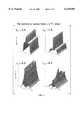
- an MFA-MOPA semiconductor laserin accord with one embodiment of the present invention, consists of a master oscillator 14, such as a distributed Bragg reflector (DBR), coupled to a trumpet-flared power amplifier 18, all formed on a common substrate 12 and with electrodes 23, 24 and 26 provided on the top and bottom surfaces of the body.
- the material compositionis some combination of group III-IV compound semiconductors, such as GaAs/AlGaAs, InGaAs/AlGaAs or InP/InGaAsP.
- group III-IV compound semiconductorssuch as GaAs/AlGaAs, InGaAs/AlGaAs or InP/InGaAsP.
- other direct bandgap semiconductor materialsmay also be used.
- the semiconductor material bodycan be formed with a homostructure, single heterostructure or, preferably, a double heterostructure or multiheterostructure. All such structures include an active light emitting region 12 near a pn junction in the body.
- This active region 12may be a single active layer, a single quantum well (SQW) structure or a multiple quantum well (MQW) structure. Strained-layer superlattice structures may be used.
- the electrodes 23, 24 and 26provide a forward electrical bias across the pn junction and inject currents I MO and I PA through the active region 12 of the master oscillator 14 and power amplifier 18 areas respectively of the MOPA device.
- a pump current greater than a lasing threshold current density injected through the active region 12 in the gain section of the MOPAcauses lightwaves to be generated in the master oscillator section and to propagate under lasing conditions.
- the active region 12 and the layers above and below itform a transverse waveguide for light propagation.
- the term “transverse”is used here to refer to the direction perpendicular to the plane of the active region 12. Lateral waveguiding is also provided in portions of the MOPA device described below.
- the term “lateral” or “x”refers to the direction in the plane of the active region perpendicular to the direction of propagation.
- the direction of laser light propagation itselfis referred to as the "longitudinal" or "z" direction.
- the diode laser oscillator 14is preferably a distributed Bragg reflector (DBR) laser defined by first or second order DBR gratings 16 bounding the pumped region of the master oscillator.
- DBRdistributed Bragg reflector
- An additional preamplifier and second set of DBR gratingscan be added between the master oscillator 14 and the power amplifier 18 to allow for adjustment of the input power to the amplifier independent from the adjustment of the output power of the master oscillator.
- a flared power amplifier 18is coupled to the master oscillator 14. As well understood in the art, gratings at the input aperture and antireflective coating at the output aperture of the amplifier are provided and designed to prevent self-oscillation.
- the flare of the power amplifier 18is a non-linear flare referred to as a "trumpet-flare.”
- the amplifier 18has a transverse waveguiding region 20 with an active light emitting gain region 12 sandwiched between adjacent, higher bandgap, lower refractive index layers above and below the active region 12.
- the amplifier 18is electrically pumped with a uniform amplification current I PA through contacts 24 and 26.
- the width of the top conductive contact 24 above the amplifier 18, and consequently the width of the gain region,is flared such that it has a first width at the input end of the amplifier 18 that substantially matches the width of the output of the master oscillator 14 and a second width at the output end of the amplifier 18 that is significantly wider than the first width.
- the increase in width in the amplifier's pumped gain region 20 of amplifier 18 defined by the contact 24 or other waveguiding meansmatches or is only slightly larger than the divergence of the light beam received from the master oscillator 14.
- the output of the power amplifier 18passes through an output facet 22 which is antireflection (AR) coated.
- the shape of the flare of the gain region of amplifier 18 illustrated in FIG. 1Ais carefully chosen to allow higher output powers from the amplifier 18 before the onset of transverse beam instabilities and filamentation.
- the trumpet-flared gain region of amplifier 18when optimized to delay the onset of filamentation, also results in a reduced amount of optical feedback from the output of the power amplifier 18 to the master oscillator 14, thereby allowing higher output powers before the onset of reflection-induced intensity and phase fluctuations.
- the optimum shape of the flare of the gain region of amplifier 18is dependent upon the geometry of the amplifier as well as the semiconductor material of the substrate 12.
- the shape of the flared gain region of amplifier 18is optimized for an MFA-MOPA embodiment according to the present invention by using a high resolution computational model developed for this purpose (see J. V. Moloney et al., "Full Space-Time Simulation for High-Brightness Semiconductor Lasers,” IEEE Photonics Technology Letters, Vol. 9, No. 6, pp. 731-733, June 1997; P. M. W. Skovgaard et al., "Enhanced Stability of MFA-MOPA Semiconductor Laser Using a Nonlinear, Trumpet-Shaped Flare," IEEE Photonics Technology Letters, Vol. 9, No. 9, pp. 1220-1222, September 1997; and C. Z.
- the modelresolves time and longitudinal and transverse space dependencies and includes realistic gain and dispersion dynamics.
- the essence of the modelis the extraction of the local refractive index and gain spectra from the complex susceptibility function ⁇ (N, ⁇ ) of the photon energy h ⁇ and of the carrier density N.
- ⁇ (N, ⁇ )is normally calculated using a detailed microscopic theory of highly excited semiconductors but may also be obtained directly from experimental data; it is fitted to a number of Lorentzians to give a detailed yet computationally tractable picture of the material response.
- Nonlinear (saturable) gain and the influence of many-body effectscan be included in the calculation of ⁇ (N, ⁇ ) for bulk and quantum-well materials.
- the symbols ⁇ , J, e, ⁇represent respectively the internal quantum efficiency, pumping current density, electron charge, and active region width.
- ⁇ 1 and D Nrepresent the carrier recombination rate and the diffusion length.
- ⁇ (N, ⁇ )is approximated by the background term plus one or more complex Lorentzian fitted to the gain and index spectra of a 90 ⁇ strained In 0 .19 Ga 0 .81 As/GaAs quantum well, used for here example only.
- Lattice temperature effectshave not been included. Since the width of the amplifier is large, and the current density over this width is constant, lattice temperature effects are expected to play a minor role in the simulations, given that their spatial length scale is much greater than that of filamentation.
- the profile width of the flareis defined using the following equation: ##EQU2## where w o is the minimum halfwidth of the flare at the input aperture z o and w max is the (maximum) halfwidth of the flare at the output facet z max .
- the basis for the optimization of the flare shapelies in the observation that the buildup of unsaturated carriers at the edge of the flared structure, near the master oscillator's pump section end, destabilizes the device and promotes filamentation instabilities which degrade device performance.
- the strong nonuniformity of carrier density under the flare sectionchanges with current pumping level and depends on the characteristics of the laser gain medium.
- the procedure for optimizing the flare geometryis carried out following successive stages.
- the bandstructure evaluated for a specific laser gain mediumis used to compute the semiconductor optical response utilizing full microscopic many-body theory, which is well described in the literature (see, for example, Haug, H. and S. W. Koch, "Quantum Theory of the Optical and Electronic Properties of Semiconductors,” World Scientific, Third Edition, 1994; S. Hughes et al., "The Influence of Electron-Hole Scattering on the Gain Spectra and the Saturation Behavior of Highly Excited Semiconductors," Solid State Communications, Vol. 100, No. 555, pp. 1-12, 1996; and W. W.
- the next stageis an iterative procedure.
- the semiconductor optical responseis fed into a laser simulation model, such as the model described by Equations (1) and (2) above, a flare shape is specified and the space-time evolution of the forward/backward intensities and the carrier densities throughout the structure are computed.
- This informationprovides a complete profile of the distribution of carriers throughout the active gain region of the amplifier, thereby making it possible for one skilled in the art to identify high density spots likely to produce filamentation.
- This informationenables the judicious modification of the flare geometry so as to reduce pumping where high densities of unsaturated carriers are found, which in turn reduces filamentation in the amplifier.
- the flare shapeis thus modified iteratively in order to minimize the presence of unsaturated carriers along the edge of the flare.
- the bowing parameter b(as well as other flare parameters, if necessary) is varied and used to generate an updated flare profile, which is then used to compute new carrier density profiles with Equations 1 and 2.
- An alternative experimental approachwould be to utilize a transparent contact (for example an Indium Tin Oxide contact) to obtain images of the spontaneous emission from the active region of the device as a function of the bias current of the power amplifier. This would give information on the carrier density and allow one to iteratively redesign the flare according to the principles of the invention, but this approach would be less reliable because of the inevitable approximation inherent with such visual inference of carrier density.
- FIGS. 6 to 9show the corrected far-field intensities for the four cases described above.
- a correctionhas been applied to offset the natural internal divergence of the MOPA output, the correction being equivalent to including a spherical lens in the appropriate location relative to the output facet 22.
- the central lobe of the far-fieldhas an angular full-width at half-maximum (FWHM) of approximately 0.4° and typically 60% of the power is contained in the central lobe.
- FWHMfull-width at half-maximum
- the invention's modification of the flare of the typical MOPA power amplifier 18 from a linear-flare to a trumpet-flareincreases the output power for the onset of filamentation in the device by a factor of 2 while maintaining a near diffraction limited output.
- the method for optimizing the shape of the flare of a flared semiconductor laser amplifier as set forth in this disclosureallows one skilled in the art to design a trumpet-flared MOPA semiconductor laser to produce a maximum useable continuous wave (CW) output power and brightness which is approximately twice that obtainable prior to the improvement of this invention.
- CWcontinuous wave
- trumpet-flared feature to control the density distribution of carriers within the gain portion of a semiconductor laser amplifiercan be applied to an amplifier which is independent of the master oscillator.
- the methods of this inventionmay be utilized to design semiconductor flared amplifiers manufactured from a variety of semiconductor materials and different device geometries. Therefore, while the present invention has been shown and described herein in what is believed to be the most practical and preferred embodiments, it is recognized that departures can be made therefrom within the scope of the invention, which is not to be limited to the details disclosed herein but is to be accorded the full scope embraced by any and all equivalent processes and products.
Landscapes
- Physics & Mathematics (AREA)
- Condensed Matter Physics & Semiconductors (AREA)
- General Physics & Mathematics (AREA)
- Electromagnetism (AREA)
- Optics & Photonics (AREA)
- Semiconductor Lasers (AREA)
Abstract
Description
Claims (14)
Priority Applications (1)
| Application Number | Priority Date | Filing Date | Title |
|---|---|---|---|
| US09/019,976US6130903A (en) | 1997-02-07 | 1998-02-06 | Trumpet-flared monolithically integrated semiconductor laser amplifier |
Applications Claiming Priority (2)
| Application Number | Priority Date | Filing Date | Title |
|---|---|---|---|
| US3785097P | 1997-02-07 | 1997-02-07 | |
| US09/019,976US6130903A (en) | 1997-02-07 | 1998-02-06 | Trumpet-flared monolithically integrated semiconductor laser amplifier |
Publications (1)
| Publication Number | Publication Date |
|---|---|
| US6130903Atrue US6130903A (en) | 2000-10-10 |
Family
ID=26692823
Family Applications (1)
| Application Number | Title | Priority Date | Filing Date |
|---|---|---|---|
| US09/019,976Expired - Fee RelatedUS6130903A (en) | 1997-02-07 | 1998-02-06 | Trumpet-flared monolithically integrated semiconductor laser amplifier |
Country Status (1)
| Country | Link |
|---|---|
| US (1) | US6130903A (en) |
Cited By (16)
| Publication number | Priority date | Publication date | Assignee | Title |
|---|---|---|---|---|
| US20030076566A1 (en)* | 2001-10-23 | 2003-04-24 | Jonathan Simon | Optical communication devices, light emission devices and optical communication methods |
| US20030202547A1 (en)* | 1998-11-25 | 2003-10-30 | Fermann Martin E. | Multi-mode fiber amplifier |
| EP1396055A4 (en)* | 2001-06-06 | 2005-05-25 | Quintessence Photonics Corp | Laser diode with an internal mirror |
| US20070002924A1 (en)* | 2005-06-30 | 2007-01-04 | Hutchinson John M | Integrated monitoring and feedback designs for external cavity tunable lasers |
| DE102008014093A1 (en)* | 2007-12-27 | 2009-07-02 | Osram Opto Semiconductors Gmbh | Edge-emitting semiconductor laser chip with at least one current barrier |
| US20130089115A1 (en)* | 2011-10-11 | 2013-04-11 | Nlight Photonics Corporation | High Power Semiconductor Laser with Phase-Matching Optical Element |
| USD702701S1 (en)* | 2012-01-19 | 2014-04-15 | Spoonjack, Llc | Display screen with graphical user interface |
| US20150092801A1 (en)* | 2012-03-13 | 2015-04-02 | Ole Bjarlin Jensen | Laser system with wavelength converter |
| US9166369B2 (en) | 2013-04-09 | 2015-10-20 | Nlight Photonics Corporation | Flared laser oscillator waveguide |
| US9214786B2 (en) | 2013-04-09 | 2015-12-15 | Nlight Photonics Corporation | Diode laser packages with flared laser oscillator waveguides |
| US10186836B2 (en) | 2014-10-10 | 2019-01-22 | Nlight, Inc. | Multiple flared laser oscillator waveguide |
| US10270224B2 (en) | 2015-06-04 | 2019-04-23 | Nlight, Inc. | Angled DBR-grating laser/amplifier with one or more mode-hopping regions |
| CN113206441A (en)* | 2021-04-30 | 2021-08-03 | 中国科学院半导体研究所 | Main oscillation power amplification laser and preparation method thereof |
| US11837838B1 (en)* | 2020-01-31 | 2023-12-05 | Freedom Photonics Llc | Laser having tapered region |
| WO2024233226A1 (en)* | 2023-05-10 | 2024-11-14 | Kyocera Sld Laser, Inc. | High power gallium and nitrogen containing laser diode devices with improved mode quality |
| US12431692B2 (en) | 2021-04-26 | 2025-09-30 | Lumentum Operations Llc | Multi-wavelength laser diode |
Citations (4)
| Publication number | Priority date | Publication date | Assignee | Title |
|---|---|---|---|---|
| US5392308A (en)* | 1993-01-07 | 1995-02-21 | Sdl, Inc. | Semiconductor laser with integral spatial mode filter |
| US5539571A (en)* | 1992-09-21 | 1996-07-23 | Sdl, Inc. | Differentially pumped optical amplifer and mopa device |
| US5657339A (en)* | 1994-12-27 | 1997-08-12 | Fuji Photo Film Co. Ltd. | Integrated optics semiconductor laser device |
| US5715268A (en)* | 1994-01-24 | 1998-02-03 | Sdl, Inc. | Laser amplifiers with suppressed self oscillation |
- 1998
- 1998-02-06USUS09/019,976patent/US6130903A/ennot_activeExpired - Fee Related
Patent Citations (5)
| Publication number | Priority date | Publication date | Assignee | Title |
|---|---|---|---|---|
| US5539571A (en)* | 1992-09-21 | 1996-07-23 | Sdl, Inc. | Differentially pumped optical amplifer and mopa device |
| US5392308A (en)* | 1993-01-07 | 1995-02-21 | Sdl, Inc. | Semiconductor laser with integral spatial mode filter |
| US5602864A (en)* | 1993-01-07 | 1997-02-11 | Sdl, Inc. | Semiconductor laser with integral spatial mode filter |
| US5715268A (en)* | 1994-01-24 | 1998-02-03 | Sdl, Inc. | Laser amplifiers with suppressed self oscillation |
| US5657339A (en)* | 1994-12-27 | 1997-08-12 | Fuji Photo Film Co. Ltd. | Integrated optics semiconductor laser device |
Non-Patent Citations (14)
| Title |
|---|
| C.Z. Ning et al., "Effective Bloch Equations for Semiconductor Lasers and Amplifiers," IEEE Journal of Quantum Electronics, vol. 33, No. 9, pp. 1543-1550, Sep. 1997. |
| C.Z. Ning et al., Effective Bloch Equations for Semiconductor Lasers and Amplifiers, IEEE Journal of Quantum Electronics, vol. 33, No. 9, pp. 1543 1550, Sep. 1997.* |
| Haug, H. and S. W. Koch, "Quantum Theory of the Optical and Electronic Properties of Semiconductors," World Scientific, Third Edition, 1994. |
| Haug, H. and S. W. Koch, Quantum Theory of the Optical and Electronic Properties of Semiconductors, World Scientific, Third Edition, 1994.* |
| J.V. Moloney et al., "Full Space-Time Simulation for High-Brightness SemiductoR Lasers," IEEE Photonics Technology Letters, vol. 9, No. 6, pp. 731-733, Jun. 1997. |
| J.V. Moloney et al., Full Space Time Simulation for High Brightness SemiconductoR Lasers, IEEE Photonics Technology Letters, vol. 9, No. 6, pp. 731 733, Jun. 1997.* |
| O Brien, et al., Operating Characteristics of a High Power Monolithically Integrated Flared Amplifier Master Oscillator Power Amplifier, IEEE Journal of Quantum Electronics, pp. 2052 2057 (1993).* |
| O'Brien, et al., "Operating Characteristics of a High-Power Monolithically Integrated Flared Amplifier Master Oscillator Power Amplifier," IEEE Journal of Quantum Electronics, pp. 2052-2057 (1993). |
| P.M.W. Skovgaard et al., "Enhanced Stability of MFA-MOPA Semiconductor Laser Using a Nonlinear, Trumpet-Shaped Flare," IEEE Photonics Technolgy Letters, vol. 9, No. 9, pp. 1220-1222, Sep. 1997. |
| P.M.W. Skovgaard et al., Enhanced Stability of MFA MOPA Semiconductor Laser Using a Nonlinear, Trumpet Shaped Flare, IEEE Photonics Technolgy Letters, vol. 9, No. 9, pp. 1220 1222, Sep. 1997.* |
| S. Hughes et al., "The Influence of Electron-Hole Scattering on the Gain Spectra and the Saturation Behavior of Highly Excited Semiconductors," Solid State Communications, vol. 100, No. 555, pp. 1-12, 1996. |
| S. Hughes et al., The Influence of Electron Hole Scattering on the Gain Spectra and the Saturation Behavior of Highly Excited Semiconductors, Solid State Communications, vol. 100, No. 555, pp. 1 12, 1996.* |
| W.W. Chow et al., "Comparison of Experimental and Theoretical GaInP Quantum Well Gain Spectra," Appl. Phys. Lett., vol. 71, No. 157, pp. 157-159, 1997. |
| W.W. Chow et al., Comparison of Experimental and Theoretical GaInP Quantum Well Gain Spectra, Appl. Phys. Lett., vol. 71, No. 157, pp. 157 159, 1997.* |
Cited By (30)
| Publication number | Priority date | Publication date | Assignee | Title |
|---|---|---|---|---|
| US8761211B2 (en)* | 1998-11-25 | 2014-06-24 | Imra America, Inc. | Multi-mode fiber amplifier |
| US20030202547A1 (en)* | 1998-11-25 | 2003-10-30 | Fermann Martin E. | Multi-mode fiber amplifier |
| US9570880B2 (en) | 1998-11-25 | 2017-02-14 | Imra America, Inc. | Multi-mode fiber amplifier |
| US9595802B2 (en) | 1998-11-25 | 2017-03-14 | Imra America, Inc. | Multi-mode fiber amplifier |
| EP1396055A4 (en)* | 2001-06-06 | 2005-05-25 | Quintessence Photonics Corp | Laser diode with an internal mirror |
| US7155131B2 (en)* | 2001-10-23 | 2006-12-26 | Avago Technologies Fiber Ip (Singapore) Pte. Ltd. | Optical communication devices, light emission devices and optical communication methods |
| US20030076566A1 (en)* | 2001-10-23 | 2003-04-24 | Jonathan Simon | Optical communication devices, light emission devices and optical communication methods |
| US20070002924A1 (en)* | 2005-06-30 | 2007-01-04 | Hutchinson John M | Integrated monitoring and feedback designs for external cavity tunable lasers |
| DE102008014093B4 (en)* | 2007-12-27 | 2020-02-06 | Osram Opto Semiconductors Gmbh | Edge-emitting semiconductor laser chip with at least one current barrier |
| US20100284434A1 (en)* | 2007-12-27 | 2010-11-11 | Osram Opto Semiconductors Gmbh | Edge emitting semiconductor laser chip having at least one current barrier |
| DE102008014093A1 (en)* | 2007-12-27 | 2009-07-02 | Osram Opto Semiconductors Gmbh | Edge-emitting semiconductor laser chip with at least one current barrier |
| US9166368B2 (en)* | 2011-10-11 | 2015-10-20 | Nlight Photonics Corporation | High power semiconductor laser with phase-matching optical element |
| US20130089115A1 (en)* | 2011-10-11 | 2013-04-11 | Nlight Photonics Corporation | High Power Semiconductor Laser with Phase-Matching Optical Element |
| USD702701S1 (en)* | 2012-01-19 | 2014-04-15 | Spoonjack, Llc | Display screen with graphical user interface |
| US20150092801A1 (en)* | 2012-03-13 | 2015-04-02 | Ole Bjarlin Jensen | Laser system with wavelength converter |
| US9685755B2 (en)* | 2012-03-13 | 2017-06-20 | Danmarks Tekniske Universitet | Laser system with wavelength converter |
| US9553424B2 (en) | 2013-04-09 | 2017-01-24 | Nlight, Inc. | Flared laser oscillator waveguide |
| US9166369B2 (en) | 2013-04-09 | 2015-10-20 | Nlight Photonics Corporation | Flared laser oscillator waveguide |
| US9214786B2 (en) | 2013-04-09 | 2015-12-15 | Nlight Photonics Corporation | Diode laser packages with flared laser oscillator waveguides |
| US10014664B2 (en) | 2013-04-09 | 2018-07-03 | Nlight, Inc. | Flared laser oscillator waveguide |
| US10063030B2 (en) | 2013-04-09 | 2018-08-28 | Nlight, Inc. | Diode laser packages with flared laser oscillator waveguides |
| US9627852B2 (en) | 2013-04-09 | 2017-04-18 | Nlight, Inc. | Diode laser packages with flared laser oscillator waveguides |
| US10186836B2 (en) | 2014-10-10 | 2019-01-22 | Nlight, Inc. | Multiple flared laser oscillator waveguide |
| US10270224B2 (en) | 2015-06-04 | 2019-04-23 | Nlight, Inc. | Angled DBR-grating laser/amplifier with one or more mode-hopping regions |
| US11837838B1 (en)* | 2020-01-31 | 2023-12-05 | Freedom Photonics Llc | Laser having tapered region |
| US20240039240A1 (en)* | 2020-01-31 | 2024-02-01 | Freedom Photonics Llc | Laser having tapered region |
| US12224554B2 (en)* | 2020-01-31 | 2025-02-11 | Freedom Photonics Llc | Laser having tapered region |
| US12431692B2 (en) | 2021-04-26 | 2025-09-30 | Lumentum Operations Llc | Multi-wavelength laser diode |
| CN113206441A (en)* | 2021-04-30 | 2021-08-03 | 中国科学院半导体研究所 | Main oscillation power amplification laser and preparation method thereof |
| WO2024233226A1 (en)* | 2023-05-10 | 2024-11-14 | Kyocera Sld Laser, Inc. | High power gallium and nitrogen containing laser diode devices with improved mode quality |
Similar Documents
| Publication | Publication Date | Title |
|---|---|---|
| Mikulla et al. | High-brightness tapered semiconductor laser oscillators and amplifiers with low-modal gain epilayer-structures | |
| US6130903A (en) | Trumpet-flared monolithically integrated semiconductor laser amplifier | |
| US20070223549A1 (en) | High-Power Optoelectronic Device with Improved Beam Quality Incorporating A Lateral Mode Filtering Section | |
| Hallman et al. | High Power $1.5\mu $ m Pulsed Laser Diode With Asymmetric Waveguide and Active Layer Near p-cladding | |
| Zink et al. | Monolithic master oscillator tilted tapered power amplifier emitting 9.5 W at 1060 nm | |
| Selmic et al. | Single frequency 1550-nm AlGaInAs-InP tapered high-power laser with a distributed Bragg reflector | |
| JP2867819B2 (en) | Multiple quantum well semiconductor laser | |
| Hallman et al. | > 25 W pulses from 1.5 μ m double‐asymmetric waveguide, 100 μ m stripe laser diode with bulk active layer | |
| Kageyama et al. | Long-wavelength quantum dot FP and DFB lasers for high temperature applications | |
| US5606570A (en) | High power antiguided semiconductor laser with interelement loss | |
| Skovgaard et al. | Enhanced stability of MFA-MOPA semiconductor lasers using a nonlinear, trumpet-shaped flare | |
| RU2540233C1 (en) | Injection laser having multiwave modulated emission | |
| Pezeshki et al. | GaInP/AlGaInP 670 nm singlemode DBR laser | |
| Agrawal et al. | Linewidth of distributed feedback semiconductor lasers with partially reflecting facets | |
| US7139299B2 (en) | De-tuned distributed feedback laser diode | |
| Kallenbach et al. | High-power high-brightness ridge-waveguide tapered diode lasers at 14xx nm | |
| Brox et al. | High-power ridge waveguide DFB and DFB-MOPA lasers at 1064 nm with a vertical farfield angle of 15 | |
| JP3010817B2 (en) | Semiconductor optical device | |
| Nilsson et al. | Improved spectral characteristics of MQW-DFB lasers by incorporation of multiple phase-shifts | |
| Belenky et al. | Trends in semiconductor laser design: Balance between leakage, gain and loss in InGaAsP/InP MQW structures | |
| Unger | High-power laser diodes and laser diode arrays | |
| Petermann | Basic laser characteristics | |
| Chazan et al. | Influence of the epitaxial layer structure on the beam quality factor of tapered semiconductor amplifiers | |
| Bedford et al. | Semiconductor unstable resonators with laterally finite mirrors | |
| Luo et al. | Tapered-cavity surface-emitting distributed-Bragg-reflector semiconductor lasers: Modeling and experiment |
Legal Events
| Date | Code | Title | Description |
|---|---|---|---|
| AS | Assignment | Owner name:ARIZONA BOARD OF REGENTS ON BEHALF OF THE UNIVERSI Free format text:ASSIGNMENT OF ASSIGNORS INTEREST;ASSIGNORS:MOLONEY, JEROME V.;INDIK, ROBERT;NING, CUN-ZHENG;REEL/FRAME:009099/0363;SIGNING DATES FROM 19980317 TO 19980323 | |
| AS | Assignment | Owner name:AIR FORCE, UNITED STATES, VIRGINIA Free format text:CONFIRMATORY LICENSE;ASSIGNOR:ARIZONA, UNIVERSITY OF;REEL/FRAME:013542/0348 Effective date:20020716 | |
| FEPP | Fee payment procedure | Free format text:PAYOR NUMBER ASSIGNED (ORIGINAL EVENT CODE: ASPN); ENTITY STATUS OF PATENT OWNER: SMALL ENTITY | |
| FPAY | Fee payment | Year of fee payment:4 | |
| FPAY | Fee payment | Year of fee payment:8 | |
| AS | Assignment | Owner name:AIR FORCE, UNITED STATES, VIRGINIA Free format text:CONFIRMATORY LICENSE;ASSIGNOR:UNIVERSITY OF ARIZONA;REEL/FRAME:027465/0419 Effective date:20020716 | |
| REMI | Maintenance fee reminder mailed | ||
| LAPS | Lapse for failure to pay maintenance fees | ||
| STCH | Information on status: patent discontinuation | Free format text:PATENT EXPIRED DUE TO NONPAYMENT OF MAINTENANCE FEES UNDER 37 CFR 1.362 | |
| FP | Lapsed due to failure to pay maintenance fee | Effective date:20121010 |