US6130732A - Paper-white reflective display and methods of forming the same - Google Patents
Paper-white reflective display and methods of forming the sameDownload PDFInfo
- Publication number
- US6130732A US6130732AUS08/792,307US79230797AUS6130732AUS 6130732 AUS6130732 AUS 6130732AUS 79230797 AUS79230797 AUS 79230797AUS 6130732 AUS6130732 AUS 6130732A
- Authority
- US
- United States
- Prior art keywords
- liquid crystal
- layers
- paper
- reflective display
- forming
- Prior art date
- Legal status (The legal status is an assumption and is not a legal conclusion. Google has not performed a legal analysis and makes no representation as to the accuracy of the status listed.)
- Expired - Lifetime
Links
- 241000533901Narcissus papyraceusSpecies0.000titleclaimsabstractdescription54
- 238000000034methodMethods0.000titleclaimsdescription19
- 239000004973liquid crystal related substanceSubstances0.000claimsabstractdescription128
- 229920000642polymerPolymers0.000claimsabstractdescription119
- 239000000758substrateSubstances0.000claimsabstractdescription24
- 239000000463materialSubstances0.000claimsdescription10
- 239000006096absorbing agentSubstances0.000claimsdescription5
- 239000005262ferroelectric liquid crystals (FLCs)Substances0.000claimsdescription3
- 239000003999initiatorSubstances0.000claimsdescription3
- 239000000178monomerSubstances0.000claimsdescription3
- 238000004873anchoringMethods0.000claims2
- 230000001939inductive effectEffects0.000claims2
- 230000005684electric fieldEffects0.000description6
- 239000004983Polymer Dispersed Liquid CrystalSubstances0.000description5
- 239000004986Cholesteric liquid crystals (ChLC)Substances0.000description4
- AMGQUBHHOARCQH-UHFFFAOYSA-Nindium;oxotinChemical compound[In].[Sn]=OAMGQUBHHOARCQH-UHFFFAOYSA-N0.000description4
- 238000002310reflectometryMethods0.000description4
- 230000003595spectral effectEffects0.000description4
- 239000002131composite materialSubstances0.000description3
- 238000005516engineering processMethods0.000description3
- 229920000106Liquid crystal polymerPolymers0.000description2
- 239000004977Liquid-crystal polymers (LCPs)Substances0.000description2
- 239000004988Nematic liquid crystalSubstances0.000description2
- BLRPTPMANUNPDV-UHFFFAOYSA-NSilaneChemical compound[SiH4]BLRPTPMANUNPDV-UHFFFAOYSA-N0.000description2
- 230000015572biosynthetic processEffects0.000description2
- 230000003098cholesteric effectEffects0.000description2
- 238000010586diagramMethods0.000description2
- 230000002452interceptive effectEffects0.000description2
- 230000003287optical effectEffects0.000description2
- 238000005457optimizationMethods0.000description2
- 229910000077silaneInorganic materials0.000description2
- 239000004094surface-active agentSubstances0.000description2
- 230000003213activating effectEffects0.000description1
- 239000000654additiveSubstances0.000description1
- 230000000996additive effectEffects0.000description1
- 238000013019agitationMethods0.000description1
- 238000000149argon plasma sinteringMethods0.000description1
- 230000001419dependent effectEffects0.000description1
- 238000011161developmentMethods0.000description1
- 230000018109developmental processEffects0.000description1
- 239000006185dispersionSubstances0.000description1
- 230000002708enhancing effectEffects0.000description1
- 239000005276holographic polymer dispersed liquid crystals (HPDLCs)Substances0.000description1
- 238000001093holographyMethods0.000description1
- 238000005286illuminationMethods0.000description1
- 238000004519manufacturing processMethods0.000description1
- 239000011159matrix materialSubstances0.000description1
- 239000000203mixtureSubstances0.000description1
- 238000012986modificationMethods0.000description1
- 230000004048modificationEffects0.000description1
- 230000000737periodic effectEffects0.000description1
- 238000005191phase separationMethods0.000description1
- 229920002959polymer blendPolymers0.000description1
- 238000007493shaping processMethods0.000description1
- 239000002904solventSubstances0.000description1
- 230000000087stabilizing effectEffects0.000description1
- 239000011800void materialSubstances0.000description1
Images


Classifications
- G—PHYSICS
- G02—OPTICS
- G02F—OPTICAL DEVICES OR ARRANGEMENTS FOR THE CONTROL OF LIGHT BY MODIFICATION OF THE OPTICAL PROPERTIES OF THE MEDIA OF THE ELEMENTS INVOLVED THEREIN; NON-LINEAR OPTICS; FREQUENCY-CHANGING OF LIGHT; OPTICAL LOGIC ELEMENTS; OPTICAL ANALOGUE/DIGITAL CONVERTERS
- G02F1/00—Devices or arrangements for the control of the intensity, colour, phase, polarisation or direction of light arriving from an independent light source, e.g. switching, gating or modulating; Non-linear optics
- G02F1/01—Devices or arrangements for the control of the intensity, colour, phase, polarisation or direction of light arriving from an independent light source, e.g. switching, gating or modulating; Non-linear optics for the control of the intensity, phase, polarisation or colour
- G02F1/13—Devices or arrangements for the control of the intensity, colour, phase, polarisation or direction of light arriving from an independent light source, e.g. switching, gating or modulating; Non-linear optics for the control of the intensity, phase, polarisation or colour based on liquid crystals, e.g. single liquid crystal display cells
- G02F1/133—Constructional arrangements; Operation of liquid crystal cells; Circuit arrangements
- G02F1/1333—Constructional arrangements; Manufacturing methods
- G02F1/1347—Arrangement of liquid crystal layers or cells in which the final condition of one light beam is achieved by the addition of the effects of two or more layers or cells
- G02F1/13471—Arrangement of liquid crystal layers or cells in which the final condition of one light beam is achieved by the addition of the effects of two or more layers or cells in which all the liquid crystal cells or layers remain transparent, e.g. FLC, ECB, DAP, HAN, TN, STN, SBE-LC cells
- G02F1/13473—Arrangement of liquid crystal layers or cells in which the final condition of one light beam is achieved by the addition of the effects of two or more layers or cells in which all the liquid crystal cells or layers remain transparent, e.g. FLC, ECB, DAP, HAN, TN, STN, SBE-LC cells for wavelength filtering or for colour display without the use of colour mosaic filters
- G—PHYSICS
- G02—OPTICS
- G02F—OPTICAL DEVICES OR ARRANGEMENTS FOR THE CONTROL OF LIGHT BY MODIFICATION OF THE OPTICAL PROPERTIES OF THE MEDIA OF THE ELEMENTS INVOLVED THEREIN; NON-LINEAR OPTICS; FREQUENCY-CHANGING OF LIGHT; OPTICAL LOGIC ELEMENTS; OPTICAL ANALOGUE/DIGITAL CONVERTERS
- G02F1/00—Devices or arrangements for the control of the intensity, colour, phase, polarisation or direction of light arriving from an independent light source, e.g. switching, gating or modulating; Non-linear optics
- G02F1/01—Devices or arrangements for the control of the intensity, colour, phase, polarisation or direction of light arriving from an independent light source, e.g. switching, gating or modulating; Non-linear optics for the control of the intensity, phase, polarisation or colour
- G02F1/13—Devices or arrangements for the control of the intensity, colour, phase, polarisation or direction of light arriving from an independent light source, e.g. switching, gating or modulating; Non-linear optics for the control of the intensity, phase, polarisation or colour based on liquid crystals, e.g. single liquid crystal display cells
- G02F1/133—Constructional arrangements; Operation of liquid crystal cells; Circuit arrangements
- G02F1/1333—Constructional arrangements; Manufacturing methods
- G02F1/1334—Constructional arrangements; Manufacturing methods based on polymer dispersed liquid crystals, e.g. microencapsulated liquid crystals
- G02F1/13342—Holographic polymer dispersed liquid crystals
- G—PHYSICS
- G02—OPTICS
- G02F—OPTICAL DEVICES OR ARRANGEMENTS FOR THE CONTROL OF LIGHT BY MODIFICATION OF THE OPTICAL PROPERTIES OF THE MEDIA OF THE ELEMENTS INVOLVED THEREIN; NON-LINEAR OPTICS; FREQUENCY-CHANGING OF LIGHT; OPTICAL LOGIC ELEMENTS; OPTICAL ANALOGUE/DIGITAL CONVERTERS
- G02F2202/00—Materials and properties
- G02F2202/02—Materials and properties organic material
- G02F2202/022—Materials and properties organic material polymeric
- G—PHYSICS
- G02—OPTICS
- G02F—OPTICAL DEVICES OR ARRANGEMENTS FOR THE CONTROL OF LIGHT BY MODIFICATION OF THE OPTICAL PROPERTIES OF THE MEDIA OF THE ELEMENTS INVOLVED THEREIN; NON-LINEAR OPTICS; FREQUENCY-CHANGING OF LIGHT; OPTICAL LOGIC ELEMENTS; OPTICAL ANALOGUE/DIGITAL CONVERTERS
- G02F2203/00—Function characteristic
- G02F2203/02—Function characteristic reflective
Definitions
- This inventionrelates to a reflective display and methods of forming the same.
- the inventionrelates to a paper-white liquid crystal reflective display and methods of forming the same.
- a reflective liquid crystal displayis the polymer-dispersed liquid crystal (PDLC) display, which operates on the principle of electrically controlled light scattering.
- PDLCpolymer-dispersed liquid crystal
- liquid crystal dropletsare embedded in a polymer matrix.
- the alignment of the liquid crystal dropletsis random, resulting in an opaque, scattering film because of the mismatch between effective refractive index of the liquid crystal with that of the polymer.
- the liquid crystal within the liquid crystal dropletsaligns parallel to the electric field and the composite material becomes transparent.
- contrast ratios in the direct-view reflective modeare in the 5-10:1 range and are strongly cell thickness dependent.
- the reflectivity of the polymer dispersed liquid crystal reflective displayis only about 12 to 15%.
- cholesteric liquid crystal displayAnother type of reflective liquid crystal display is the polymer dispersed cholesteric liquid crystal display (PDCLC), which operates on the principle of Bragg reflection.
- PDCLCpolymer dispersed cholesteric liquid crystal display
- Such cholesteric liquid crystal displayshave a contrast ratio approaching approximately 10:1 with a photopic reflectivity of 10-13% under ambient lighting conditions and approximately 40% peak reflectivity at the Bragg wavelength.
- Another type of reflective liquid crystal displayis a polymer stabilized cholesteric texture (PSCT) reflective display.
- PSDpolymer stabilized cholesteric texture
- the polymer stabilized cholesteric texture reflective displayuses a small amount of polymer additive in the cholesteric liquid crystal medium which assembles into an ordered stabilizing network. Contrast ratios have been reported between 20-30:1 with 10 to 15% photopic reflection under ambient lighting conditions, and nearly 40% peak reflectivity at the Bragg wavelength. Similar displays have been demonstrated without the polymer with comparable performance.
- a more recent type of reflective liquid crystal displayis the holographic polymer dispersed liquid crystal display.
- Such a displayis reported in "Holographically formed liquid crystal/polymer device for reflective color displays", by Tanaka et al., as reported in the Journal of the Society for Information Display, Volume 2, No. 1, 1994, pages 37-40. Further developments by Tanaka et al. reported on optimization of such a holographic liquid crystal display in "Optimization of Holographic PDLC for Reflective Color Display Applications" in the SID '95 Digest, pages 267-270.
- This holographically formed polymer dispersed liquid crystalis formed using optical interference techniques (reflection holography) to form planes of liquid crystal droplets at predesignated positions within the sample setting up a modulation in the liquid crystal droplet densities.
- the resulting optical interferencereflects the Bragg wavelength in the off-state when the liquid crystal material directors encapsulated within the droplets are misaligned.
- the periodic refractive index modulationvanishes if the refractive index of the liquid crystal is approximately matched with the refractive index of the polymer, and all incident light is transmitted.
- the spectral reflectance of the displayis determined during the fabrication process and can be chosen to reflect any visible wavelength.
- the above-described holographic liquid crystal/polymer reflective color displayis formed with an isotropic polymer which results in liquid crystal droplets being formed during the phase separation. Because the polymer is isotropic, the molecules of the polymer are randomly aligned and the display device has visible opaqueness or haze when viewed from an angle due to the mismatch between the effective refractive index of the liquid crystal and that of the polymer becomes enhanced at wide angles. Additionally, this display device requires a relatively large drive voltage due to the liquid crystal spherical droplets. In particular, the voltage necessary to drive the display device is proportional to the surface-to-volume ratio of the liquid crystal droplets. Such spherical droplets have a surface-to-volume ratio of 3/R where R is the radius of the droplet.
- U.S. patent application attorney docket No. JAO 34133entitled “HOLOGRAPHICALLY FORMED REFLECTIVE DISPLAY, LIQUID CRYSTAL DISPLAY AND PROJECTION SYSTEMS AND METHODS OF FORMING THE SAME", the subject matter of which is incorporated herein, discloses holographically formed reflective displays and projection systems.
- U.S. Patent application attorney docket No. JAO 34134entitled “BROADBAND REFLECTIVE DISPLAY AND METHODS OF FORMING THE SAME”, the subject matter of which is incorporated herein, discloses broadening the reflective wavelengths by including a plurality of groups of reflective layers each being reflective of different wavelengths of light.
- this inventionprovides a paper-white reflective display that has improved photopic white reflectance, a high contrast, a lack of haze or opaqueness when viewed from various viewing angles and a reduced drive voltage compared to conventional devices.
- the paper-white reflective displayincludes first and second substrates, a plurality of groups of liquid crystal and polymer layers located between the first and second substrates, each of the plurality of groups of liquid crystal and polymer layers being reflective of different wavelengths of light and a voltage source connected between the first and second substrates that selectively applies a voltage to all of the liquid crystal and polymer layers.
- FIG. 1ais a schematic view illustrating a reflective display prior to application of interfering lasers during assembly of the display
- FIG. 1bis a schematic view illustrating the reflective display
- FIGS. 2a-2cillustrate the homogenous and homeotropic surface boundary conditions of the reflective display in the off-state
- FIGS. 3a-3cillustrate the homogenous and homeotropic surface boundary conditions of the reflective display in the on-state
- FIG. 4illustrates a full-color reflective liquid crystal display
- FIG. 5illustrates a projection system which includes three reflective displays
- FIG. 6illustrates a paper-white reflective display
- FIGS. 7a and 7bare graphs illustrating reflectance versus wavelength and a diagram showing the chromaticity of the white-point, respectively, for the paper-white reflective display of FIG. 6;
- FIG. 8illustrates a paper-white reflective display having a plurality of sub-layers
- FIGS. 9a and 9bare graphs illustrating reflectance versus wavelength and a diagram showing the chromaticity of the white-point, respectively, for the paper-white reflective display of FIG. 8.
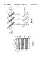
- FIG. 1aillustrates a reflective display.
- Alignment layers 14may be a rubbed polymer layer, where homogeneous surface boundary conditions are desired, or a silane surfactant layer, for example, where homeotropic (perpendicular) surface boundary conditions are desired, as will be further explained below.
- Displaced between the alignment layers 14is a anisotropic polymer 18 dissolved in a liquid crystal solvent.
- the anisotropic polymer 18may include a photo-active monomer and suitable photo-initiator.
- the liquid crystal polymer mixture 16is homogenized via mechanical agitation and heat.
- the deviceis then irradiated with interfering laser beams A and B, for example, that set up interference fringes within the device.
- the resultant structureis illustrated in FIG. 1b. Regions within the liquid crystal/polymer mixture 16 that experience the high intensity of the interference pattern of the lasers become polymer rich and form polymer sheets 20 and those regions where the intensity is low become void of polymer and form liquid crystal regions 22. As can be seen in Figure 1b, the polymer sheets 20 and liquid crystal regions 22 form into a multilayer structure.
- the holographically formed reflective display 8is illustrated in FIG. 2a in an off-state.
- the off-stateoccurs when no electric field is applied between the indium tin oxide layers 12.
- the displayIn the off-state, the display is transparent and all light is transmitted through the display because the molecules of the liquid crystal regions 22 are effectively index matched and aligned with the molecules forming the polymer sheets 20.
- FIGS. 2b and 2care enlarged views of the liquid crystal layer 22 and polymer sheets 20 within circles 15 and 17 of FIGS. 2a and 3a, respectively.
- FIG. 2billustrates the homogeneous surface boundary conditions that are formed when the alignment layer 14 is a rubbed polymer layer.
- a rubbed polymer layeris well known to those of ordinary skill in the art and is formed by conventional rubbing techniques.
- the rubbed polymer layercauses the molecules within the polymer sheets 20 and within the liquid crystal regions 22 to form along the planar alignment direction of the nematic liquid crystal medium in a direction generally parallel to a surface of the substrate 10. As may be seen with reference to FIG.
- the polymer molecules forming the polymer sheets 20are anisotropic polymer molecules, the molecules are elongated and align in a single direction.
- the molecules forming liquid crystal regions 22are anisotropic and hence align in the same direction as the molecules forming the polymer sheets.
- This index matched alignmentvastly reduces haze in the holographically formed reflective display 8 when it is viewed from various viewing angles.
- Conventional holographically formed reflective displaysin contrast, use isotropic polymers which are randomly aligned and thus create haze and opaqueness when viewed from various viewing angles.
- FIG. 2cis an enlarged view of the circle 15 shown in FIG. 2a.
- the homeotropic surface boundary conditionsare created when the alignment layer 14 includes perpendicular alignment.
- One exampleis a silane surfactant layer. This causes the anisotropic polymer within the polymer sheets 20 to align substantially perpendicular to a surface of the substrates 10 as illustrated in FIG. 2C.
- the molecules within the liquid crystal region 22are anisotropic, they align in the same direction as the anisotropic polymer molecules forming the polymer sheets 20.
- use of the anisotropic polymergreatly reduces haze and opaqueness in the holographically formed reflective display 8 when viewed from various viewing angles.
- FIG. 3aillustrates the holographically formed reflective display 8 in an on-state.
- a voltage from a voltage source 24is applied between the indium tin oxide layers 12. This creates an electric field in the direction illustrated by arrow E and causes the display to be reflective of light of a desired wavelength.
- the desired wavelength of the reflected lightmay be selected during formation of the device by appropriately controlling the wavelengths of the interference fringes created by the laser or other holograhic means used during device formation.
- FIG. 3bis an enlarged view of the area shown within circle 17 in FIG. 3a for homogenous surface boundary conditions.
- Application of the electric field E between the indium tin oxide layerscauses molecules with positive dielective anisotropy within the liquid crystal regions 22 to align parallel to the E direction, as illustrated in FIG. 3b. This causes light of a desired wavelength to be reflected while all other light is transmitted.
- FIG. 3cHomeotropic surface boundary conditions for the holographically formed reflective display 8 in the on-state are illustrated in FIG. 3c.
- the liquid crystal material usedis one with negative dielectric anisotropy.
- application of the electric field Ecauses the molecules with negative dielectric anisotropy within the liquid crystal region 22 to align perpendicular to the E field direction causing light of the desired wavelength to be reflected.
- a full-color liquid crystal displayis illustrated in FIG. 4.
- the liquid crystal material usedis one with positive dielectic anisotropy.
- the full-color liquid crystal display 26includes three holographically formed reflective displays 25, 27 and 29 (which are similar to the holographically formed reflective display 8) each being reflective of a different wavelength of light.
- the full-color liquid crystal display 26includes black absorber 28 which is used to absorb non-reflective wavelengths and enhance display contrasts.
- ambient lightis exposed to the upper surface 31 of the full-color liquid crystal display 26 in the direction of arrow F.
- the voltage sources 24are each independently controlled to selectively reflect light from each of the holographically formed reflective displays 8, each reflecting light of a different wavelength.
- the upper reflective display 25 in FIG. 4may reflect light of 465 nm
- the middle holographically formed reflective display 27may reflect light of 545 nm
- the lower holographically formed reflective display 29may reflect light of 620 nm, to reflect light of blue, green and red wavelengths, respectively.
- FIG. 5illustrates a full-color projection system 31 which includes a first holographically formed reflective display 30, which may selectively reflect red light having an approximate wavelength of 620 nm, a second holographically formed reflective display 32, which may reflect green light of approximately 545 nm and a third holographically formed reflective display 34, which may reflect blue light of approximately 465 nm.
- a first holographically formed reflective display 30which may selectively reflect red light having an approximate wavelength of 620 nm
- a second holographically formed reflective display 32which may reflect green light of approximately 545 nm
- a third holographically formed reflective display 34which may reflect blue light of approximately 465 nm.
- Lightis input from a light source 36 and upon contacting the first holographically formed reflective display 30, red light having a wavelength of approximately 620 nm is reflected in the direction of arrow G onto mirror 38 and reflected towards an output in a direction of arrow H.
- Light which is not of the red wavelength of approximately 620 nmis transmitted by the first holographically formed reflective display 30 in the direction of arrow I to the second holographically formed reflective display 32.
- the second holographically formed reflective display 32reflects light with a green wavelength of approximately 545 nm in the direction of arrow J onto a surface of first dichroic mirror 40.
- First dichroic wavelength mirror 40transmits the red light reflected by mirror 38 and reflects the green light in a direction of arrow H.
- Second dichroic mirror 42reflects the blue wavelength light in the direction of arrow H and transmits the red and green light from mirror 38 and first dichroic mirror 40 to the output. In this way, an image may be formed and projected by the full-color projection system 31.
- the above-noted reflective wavelengths for the first, second and third holographically formed reflective displays 30, 32 and 34 of the projection system 31may be varied to the desired value by adjusting the wavelength of light that is reflected by each display to a desired value, as discussed above regarding the FIG. 2a-3c embodiment.
- holographically formed reflective displaysmay achieve bistable switching by using a chiral nematic or ferroelectric liquid crystal material instead of a typical nematic liquid crystal material which would normally be used.
- Bistabilityis more fully discussed in a related application entitled “Bistable Reflective Display Using Chiral Liquid Crystal and Reconfigurable Inorganic Agglomerates” (Attorney Docket No. JAO 34136), the subject matter of which is incorporated herein by reference in its entirety.
- FIG. 6illustrates a paper-white reflective display 47.
- the paper-white reflective display 47is similar to the reflective display 26 of FIG. 4 except that the paper-white reflective display 47 includes only two substrates 48 and 50 between which three groups of liquid crystal and polymer layers 52, 54 and 56 are formed.
- Each of the groups of liquid crystal and polymer layers 52, 54 and 56may include one liquid crystal layer and one polymer layer or a plurality of liquid crystal layers and a plurality of polymer layers, in the same manner as illustrated in Fig. 1b, for example.
- Each of the groups of liquid crystal and polymer layers 52, 54 and 56are formed as discussed above to be reflective of different wavelengths of light.
- the group of liquid crystal and polymer layers 52may be reflective of red light having a center wavelength of approximately 630 nm
- the group of liquid crystal and polymer layers 54may be reflective of green light having a center wavelength of approximately 540 nm
- the group of liquid crystal and polymer layers 56may be reflective of blue light having a center wavelength of approximately 480 nm.
- the paper-white reflective display 47will cause all of the groups of liquid crystal and polymer layers 52, 54 and 56 to be reflective or transparent at any given time.
- the paper-white reflective display 47takes on a paper-white appearance due to the combination of red, green and blue light all being simultaneously reflected.
- the paper-white reflective display 47also includes a black absorber 60 formed adjacent to substrate 50.
- the black absorber 60acts as a light stop which absorbs non-reflected wavelengths, thereby enhancing display contrast and giving the display a black appearance when the liquid crystal and polymer layers 52, 54 and 56 are in a transparent state.
- FIG. 7ais a composite reflectance versus wavelength graph illustrating the reflectance of the paper-white reflective display 47 with the groups of liquid crystal and polymer layers 52, 54 and 56 being reflective of the above-described center wavelengths of light, each group being reflective of light having an approximately 40 nm bandwidth.
- FIG. 7bis a chromaticity chart of the paper-white reflective display 47 and illustrates the chromaticity value for the display white-point for the paper-white reflective display 47 and its desired proximity to D50 and D65 standard illuminants. The photopic reflectance of the white state is approximately 44%, as noted in FIG. 7b.
- FIG. 8illustrates paper-white reflective display 62.
- the paper-white reflective display 62includes a plurality of liquid crystal and polymer sub-layers each being reflective of a different wavelength of light.
- the illustrated embodimentincludes nine liquid crystal and polymer sub-layers 70-86, three for each group. However, different numbers of groups or sub-layers may be used. The groups and sub-layers are tuned to particular wavelengths as described above regarding the FIG. 2a-3c embodiment.
- the group of liquid crystal and polymer layers 64includes three liquid crystal and polymer sub-layers 70, 72 and 74 each being reflective of red wavelengths of light, but having their central wavelengths shifted from one another to broaden the spectral reflectance.
- the three liquid crystal and polymer sub-layers 70, 72 and 74may have central wavelengths of 600 nm, 630 nm and 660 nm, respectively.
- the group of liquid crystal and polymer layers 66includes three liquid crystal and polymer sub-layers 76, 78 and 80 each being reflective of green wavelengths of light, but having their central wavelengths shifted from one another to broaden the spectral reflectance.
- the three liquid crystal and polymer sub-layers 76, 78 and 80may have central wavelengths of 510 nm, 540 nm and 570 nm, respectively.
- the group of liquid crystal and polymer layers 68includes three liquid crystal and polymer sub-layers 82, 84 and 86 each being reflective of blue wavelengths of light, but having their central wavelengths shifted from one another to broaden the spectral reflectance.
- the three liquid crystal and polymer sub-layers 82, 84 and 86may have central wavelengths of 460 nm, 480 nm and 500 nm, respectively.
- Each of the liquid crystal and polymer sub-layersmay have a 40 nm bandwidth.
- FIG. 9ais a composite reflectance versus wavelength graph illustrating the reflectance of the paper-white reflective display 62.
- the relative reflectance values of the green, red and blue peakshave been adjusted 9a to achieve the desired white-point chromaticity. Because this embodiment greatly increases the bandwidth of the reflectance peaks compared to the reflective display of FIG. 6, the photopic white reflectance is increased to 73%.
- FIG. 9bis a chromaticity chart of the paper-white reflective display 62 and as illustrated, produces a desired white-point chromaticity in close proximity to the D50 and D65 standard illuminants.
Landscapes
- Physics & Mathematics (AREA)
- Nonlinear Science (AREA)
- Mathematical Physics (AREA)
- Chemical & Material Sciences (AREA)
- Crystallography & Structural Chemistry (AREA)
- General Physics & Mathematics (AREA)
- Optics & Photonics (AREA)
- Liquid Crystal (AREA)
- Holo Graphy (AREA)
- Devices For Indicating Variable Information By Combining Individual Elements (AREA)
Abstract
Description
Claims (26)
Priority Applications (4)
| Application Number | Priority Date | Filing Date | Title |
|---|---|---|---|
| US08/792,307US6130732A (en) | 1997-01-31 | 1997-01-31 | Paper-white reflective display and methods of forming the same |
| DE69815560TDE69815560T2 (en) | 1997-01-31 | 1998-01-23 | Reflective liquid crystal display device and method of manufacturing the same |
| EP98300468AEP0856765B1 (en) | 1997-01-31 | 1998-01-23 | Reflective-type liquid crystal display and methods of forming the same |
| JP01630298AJP4462651B2 (en) | 1997-01-31 | 1998-01-29 | Paper white reflective display |
Applications Claiming Priority (1)
| Application Number | Priority Date | Filing Date | Title |
|---|---|---|---|
| US08/792,307US6130732A (en) | 1997-01-31 | 1997-01-31 | Paper-white reflective display and methods of forming the same |
Publications (1)
| Publication Number | Publication Date |
|---|---|
| US6130732Atrue US6130732A (en) | 2000-10-10 |
Family
ID=25156446
Family Applications (1)
| Application Number | Title | Priority Date | Filing Date |
|---|---|---|---|
| US08/792,307Expired - LifetimeUS6130732A (en) | 1997-01-31 | 1997-01-31 | Paper-white reflective display and methods of forming the same |
Country Status (4)
| Country | Link |
|---|---|
| US (1) | US6130732A (en) |
| EP (1) | EP0856765B1 (en) |
| JP (1) | JP4462651B2 (en) |
| DE (1) | DE69815560T2 (en) |
Cited By (8)
| Publication number | Priority date | Publication date | Assignee | Title |
|---|---|---|---|---|
| US6392725B1 (en)* | 1997-11-18 | 2002-05-21 | Fuji Xerox Co., Ltd. | Systems and methods for providing a storage medium |
| US6646710B2 (en)* | 2000-04-27 | 2003-11-11 | Fuji Xerox Co., Ltd. | Light modulator |
| US6803899B1 (en)* | 1999-07-27 | 2004-10-12 | Minolta Co., Ltd. | Liquid crystal display apparatus and a temperature compensation method therefor |
| WO2007118306A1 (en)* | 2006-04-19 | 2007-10-25 | The University Of British Columbia | Ionic electrophoresis in tir-modulated reflective image displays |
| US20100231997A1 (en)* | 2009-03-10 | 2010-09-16 | Drexel University | Dynamic time multiplexing fabrication of holographic polymer dispersed liquid crystals for increased wavelength sensitivity |
| US9576694B2 (en) | 2010-09-17 | 2017-02-21 | Drexel University | Applications for alliform carbon |
| US9752932B2 (en) | 2010-03-10 | 2017-09-05 | Drexel University | Tunable electro-optic filter stack |
| US20180311937A1 (en)* | 2015-06-30 | 2018-11-01 | Gauzy Ltd | Multiple and single layers liquid crystal dispersion devices for common and direct glazing applications and methods thereof |
Families Citing this family (13)
| Publication number | Priority date | Publication date | Assignee | Title |
|---|---|---|---|---|
| US7077984B1 (en) | 1996-07-12 | 2006-07-18 | Science Applications International Corporation | Electrically switchable polymer-dispersed liquid crystal materials |
| US5942157A (en) | 1996-07-12 | 1999-08-24 | Science Applications International Corporation | Switchable volume hologram materials and devices |
| US7312906B2 (en) | 1996-07-12 | 2007-12-25 | Science Applications International Corporation | Switchable polymer-dispersed liquid crystal optical elements |
| US6867888B2 (en) | 1996-07-12 | 2005-03-15 | Science Applications International Corporation | Switchable polymer-dispersed liquid crystal optical elements |
| US6821457B1 (en) | 1998-07-29 | 2004-11-23 | Science Applications International Corporation | Electrically switchable polymer-dispersed liquid crystal materials including switchable optical couplers and reconfigurable optical interconnects |
| US6317189B1 (en)* | 1998-12-29 | 2001-11-13 | Xerox Corporation | High-efficiency reflective liquid crystal display |
| WO2001038906A2 (en)* | 1999-11-23 | 2001-05-31 | Digilens, Inc. | Optical retro-reflection device |
| US6730442B1 (en) | 2000-05-24 | 2004-05-04 | Science Applications International Corporation | System and method for replicating volume holograms |
| US7619739B1 (en) | 2002-08-29 | 2009-11-17 | Science Applications International Corporation | Detection and identification of biological agents using Bragg filters |
| US7018563B1 (en) | 2002-11-26 | 2006-03-28 | Science Applications International Corporation | Tailoring material composition for optimization of application-specific switchable holograms |
| US6950173B1 (en) | 2003-04-08 | 2005-09-27 | Science Applications International Corporation | Optimizing performance parameters for switchable polymer dispersed liquid crystal optical elements |
| US7855705B2 (en)* | 2007-07-03 | 2010-12-21 | 3M Innovative Properties Company | Color liquid crystal display panel design |
| US8848294B2 (en) | 2010-05-20 | 2014-09-30 | Qualcomm Mems Technologies, Inc. | Method and structure capable of changing color saturation |
Citations (3)
| Publication number | Priority date | Publication date | Assignee | Title |
|---|---|---|---|---|
| US4596445A (en)* | 1983-03-30 | 1986-06-24 | Manchester R & D Partnership | Colored encapsulated liquid crystal apparatus using enhanced scattering |
| US5200845A (en)* | 1989-10-31 | 1993-04-06 | University Of Hawaii At Manoa | Color liquid crystal display consisting of polymer-dispersed chiral liquid crystal having negative dielectric anisotropy |
| US5748272A (en)* | 1993-02-22 | 1998-05-05 | Nippon Telegraph And Telephone Corporation | Method for making an optical device using a laser beam interference pattern |
- 1997
- 1997-01-31USUS08/792,307patent/US6130732A/ennot_activeExpired - Lifetime
- 1998
- 1998-01-23DEDE69815560Tpatent/DE69815560T2/ennot_activeExpired - Lifetime
- 1998-01-23EPEP98300468Apatent/EP0856765B1/ennot_activeExpired - Lifetime
- 1998-01-29JPJP01630298Apatent/JP4462651B2/ennot_activeExpired - Lifetime
Patent Citations (4)
| Publication number | Priority date | Publication date | Assignee | Title |
|---|---|---|---|---|
| US4596445A (en)* | 1983-03-30 | 1986-06-24 | Manchester R & D Partnership | Colored encapsulated liquid crystal apparatus using enhanced scattering |
| US5200845A (en)* | 1989-10-31 | 1993-04-06 | University Of Hawaii At Manoa | Color liquid crystal display consisting of polymer-dispersed chiral liquid crystal having negative dielectric anisotropy |
| US5748272A (en)* | 1993-02-22 | 1998-05-05 | Nippon Telegraph And Telephone Corporation | Method for making an optical device using a laser beam interference pattern |
| US5751452A (en)* | 1993-02-22 | 1998-05-12 | Nippon Telegraph And Telephone Corporation | Optical devices with high polymer material and method of forming the same |
Non-Patent Citations (18)
| Title |
|---|
| "Wide-Angle View PDLC Displays", J. W. Doans et al., Liquid Crystal Institute and Department of Physics, Kent State University--Pacific Polymer Preprint- pp. 245-247- 1989. |
| Gregory P. Crawford and Slobodan Zumer, eds., Liquid Crystals in Complex Geometries , 1996: Chapter 5, D. K. Yang et al., Polymer Stabilized Cholesteric Textures, pp. 103 142; Chapter 11, J. L. West, The Challenge of New Applications to Liquid Crystal Displays, pp. 255 264; Chapter 12, H. Yuan, Bistable Reflective Cholesteric Displays, pp. 265 280; and Chapter 15, M. Kreuzer et al., Filled Nematics, pp. 307 324.* |
| Gregory P. Crawford and Slobodan Zumer, eds., Liquid Crystals in Complex Geometries, 1996: Chapter 5, D.-K. Yang et al., "Polymer-Stabilized Cholesteric Textures," pp. 103-142; Chapter 11, J. L. West, "The Challenge of New Applications to Liquid Crystal Displays," pp. 255-264; Chapter 12, H. Yuan, "Bistable Reflective Cholesteric Displays," pp. 265-280; and Chapter 15, M. Kreuzer et al., "Filled Nematics," pp. 307-324. |
| Gregory P. Crawford et al., "Reflective Color Displays for Imaging Applications," Proceedings of the IS&T/SID 1995 Color Imaging Conference: Color Science, Systems and Applications, pp. 52-58. |
| Gregory P. Crawford et al., Reflective Color Displays for Imaging Applications, Proceedings of the IS&T/SID 1995 Color Imaging Conference: Color Science, Systems and Applications, pp. 52 58.* |
| K. Tanaka et al., "A Liquid-Crystal/Polymer Optical Device Formed by Holography for Reflective Color Display Applications," PDLC-2, pp. 109-111. |
| K. Tanaka et al., "Optimization of Holographic PDLC for Reflective Color Display Applications," SID 95 Digest, pp. 267-270. |
| K. Tanaka et al., 18.1: Optimization of Holographic PDLC for Reflective Color Display Applications , SID 95 Digest, pp. 267 270.* |
| K. Tanaka et al., 18.1: Optimization of Holographic PDLC for Reflective Color Display Applications, SID 95 Digest, pp. 267-270. |
| K. Tanaka et al., A Liquid Crystal/Polymer Optical Device Formed by Holography for Reflective Color Display Applications, PDLC 2, pp. 109 111.* |
| K. Tanaka et al., Holographically formed liquid crystal/polymer device for reflective color display , Journal of the Society for Information Display, vol. 2, No. 1, Apr. 1, 1994, pp. 37 40.* |
| K. Tanaka et al., Holographically formed liquid-crystal/polymer device for reflective color display, Journal of the Society for Information Display, vol. 2, No. 1, Apr. 1, 1994, pp. 37-40. |
| K. Tanaka et al., Optimization of Holographic PDLC for Reflective Color Display Applications, SID 95 Digest, pp. 267 270.* |
| M. Date et al., "Three-Primary-Color Holographic Polymer Dispersed Liquid Crystal (HPDLC) Devices for Reflective Displays," ASIA Display '95, pp. 603-606. |
| M. Date et al., Three Primary Color Holographic Polymer Dispersed Liquid Crystal (HPDLC) Devices for Reflective Displays, ASIA Display 95, pp. 603 606.* |
| M. Kreuzer et al., "New Liquid Crystal Display with Bistability and Selective Erasure Using Scattering in Filled Nematics," Appl. Phys. Lett. 62(15), Apr. 12, 1993, pp. 1712-1714. |
| M. Kreuzer et al., New Liquid Crystal Display with Bistability and Selective Erasure Using Scattering in Filled Nematics, Appl. Phys. Lett . 62(15), Apr. 12, 1993, pp. 1712 1714.* |
| Wide Angle View PDLC Displays , J. W. Doans et al., Liquid Crystal Institute and Department of Physics, Kent State University Pacific Polymer Preprint pp. 245 247 1989.* |
Cited By (13)
| Publication number | Priority date | Publication date | Assignee | Title |
|---|---|---|---|---|
| US6392725B1 (en)* | 1997-11-18 | 2002-05-21 | Fuji Xerox Co., Ltd. | Systems and methods for providing a storage medium |
| US6803899B1 (en)* | 1999-07-27 | 2004-10-12 | Minolta Co., Ltd. | Liquid crystal display apparatus and a temperature compensation method therefor |
| US6646710B2 (en)* | 2000-04-27 | 2003-11-11 | Fuji Xerox Co., Ltd. | Light modulator |
| US8040591B2 (en) | 2006-04-19 | 2011-10-18 | The University Of British Columbia | Ionic electrophoresis in TIR-modulated reflective image displays |
| US20090262414A1 (en)* | 2006-04-19 | 2009-10-22 | The University Of British Columbia | Ionic electrophoresis in tir-modulated reflective image displays |
| WO2007118306A1 (en)* | 2006-04-19 | 2007-10-25 | The University Of British Columbia | Ionic electrophoresis in tir-modulated reflective image displays |
| US20100231997A1 (en)* | 2009-03-10 | 2010-09-16 | Drexel University | Dynamic time multiplexing fabrication of holographic polymer dispersed liquid crystals for increased wavelength sensitivity |
| US9625878B2 (en)* | 2009-03-10 | 2017-04-18 | Drexel University | Dynamic time multiplexing fabrication of holographic polymer dispersed liquid crystals for increased wavelength sensitivity |
| US9752932B2 (en) | 2010-03-10 | 2017-09-05 | Drexel University | Tunable electro-optic filter stack |
| US9576694B2 (en) | 2010-09-17 | 2017-02-21 | Drexel University | Applications for alliform carbon |
| US10175106B2 (en) | 2010-10-29 | 2019-01-08 | Drexel University | Tunable electro-optic filter stack |
| US20180311937A1 (en)* | 2015-06-30 | 2018-11-01 | Gauzy Ltd | Multiple and single layers liquid crystal dispersion devices for common and direct glazing applications and methods thereof |
| US12291009B2 (en) | 2015-06-30 | 2025-05-06 | Gauzy Ltd. | Multiple and single layers liquid crystal dispersion devices for common and direct glazing applications and methods thereof |
Also Published As
| Publication number | Publication date |
|---|---|
| EP0856765B1 (en) | 2003-06-18 |
| JP4462651B2 (en) | 2010-05-12 |
| EP0856765A1 (en) | 1998-08-05 |
| DE69815560T2 (en) | 2003-12-11 |
| JPH10222047A (en) | 1998-08-21 |
| DE69815560D1 (en) | 2003-07-24 |
Similar Documents
| Publication | Publication Date | Title |
|---|---|---|
| US5875012A (en) | Broadband reflective display, and methods of forming the same | |
| US6133971A (en) | Holographically formed reflective display, liquid crystal display and projection system and methods of forming the same | |
| US5956113A (en) | Bistable reflective display and methods of forming the same | |
| US6130732A (en) | Paper-white reflective display and methods of forming the same | |
| US6317189B1 (en) | High-efficiency reflective liquid crystal display | |
| US5200845A (en) | Color liquid crystal display consisting of polymer-dispersed chiral liquid crystal having negative dielectric anisotropy | |
| US5726723A (en) | Sub-twisted nematic liquid crystal display | |
| US6078370A (en) | Method of constructing an array of pixels for use in a multi-pixel liquid crystal display | |
| WO1997028482A9 (en) | Twisted type nematic liquid crystal display | |
| US6144432A (en) | Reflective liquid crystal display device | |
| US5691790A (en) | Colored liquid crystal display having a reflector which reflects different wavelengths of light for different incident angles | |
| US7079207B2 (en) | Liquid crystal display | |
| JP3310569B2 (en) | Reflective liquid crystal display | |
| JP2004046178A (en) | Liquid crystal display | |
| JPH03209425A (en) | color lcd display | |
| US7196752B2 (en) | Cholesteric liquid crystal color filter with protrusions and associated methods of manufacture | |
| JPH09218421A (en) | Reflection type liquid crystal display device | |
| JP3620312B2 (en) | Liquid crystal display | |
| US20020005930A1 (en) | A liquid crystal layer including a dichroic dye | |
| JP2778297B2 (en) | Reflective liquid crystal display device and driving method thereof | |
| JPH07239471A (en) | Reflective liquid crystal display | |
| JPH10239668A (en) | Reflective liquid crystal display | |
| JPH10274780A (en) | Reflection type liquid crystal display device and driving method thereof | |
| JPH06301005A (en) | Screen | |
| KR100213182B1 (en) | Liquid crystal display element employing micro color lens |
Legal Events
| Date | Code | Title | Description |
|---|---|---|---|
| AS | Assignment | Owner name:XEROX CORPORATION, CONNECTICUT Free format text:ASSIGNMENT OF ASSIGNORS INTEREST;ASSIGNORS:CRAWFORD, GREG P.;FISKE, THOMAS G.;SILVERSTEIN, LOUIS D.;REEL/FRAME:009011/0772 Effective date:19970131 | |
| STCF | Information on status: patent grant | Free format text:PATENTED CASE | |
| AS | Assignment | Owner name:BANK ONE, NA, AS ADMINISTRATIVE AGENT, ILLINOIS Free format text:SECURITY INTEREST;ASSIGNOR:XEROX CORPORATION;REEL/FRAME:013153/0001 Effective date:20020621 | |
| AS | Assignment | Owner name:JPMORGAN CHASE BANK, AS COLLATERAL AGENT, TEXAS Free format text:SECURITY AGREEMENT;ASSIGNOR:XEROX CORPORATION;REEL/FRAME:015134/0476 Effective date:20030625 Owner name:JPMORGAN CHASE BANK, AS COLLATERAL AGENT,TEXAS Free format text:SECURITY AGREEMENT;ASSIGNOR:XEROX CORPORATION;REEL/FRAME:015134/0476 Effective date:20030625 | |
| FPAY | Fee payment | Year of fee payment:4 | |
| FPAY | Fee payment | Year of fee payment:8 | |
| AS | Assignment | Owner name:XEROX CORPORATION, NEW YORK Free format text:RELEASE BY SECURED PARTY;ASSIGNOR:JP MORGAN CHASE BANK, NA;REEL/FRAME:020540/0463 Effective date:20061204 Owner name:XEROX CORPORATION, NEW YORK Free format text:RELEASE BY SECURED PARTY;ASSIGNOR:BANK ONE, NA;REEL/FRAME:020540/0850 Effective date:20030625 | |
| AS | Assignment | Owner name:XEROX CORPORATION, NEW YORK Free format text:RELEASE BY SECURED PARTY;ASSIGNOR:JP MORGAN CHASE BANK, N.A., SUCCESSOR BY MERGER TO BANK ONE NA;REEL/FRAME:021291/0248 Effective date:20071129 | |
| AS | Assignment | Owner name:THOMSON LICENSING LLC, NEW JERSEY Free format text:ASSIGNMENT OF ASSIGNORS INTEREST;ASSIGNORS:XEROX CORPORATION;PALO ALTO RESEARCH CENTER INCORPORATED;REEL/FRAME:022575/0761;SIGNING DATES FROM 20080804 TO 20080805 Owner name:THOMSON LICENSING, FRANCE Free format text:ASSIGNMENT OF ASSIGNORS INTEREST;ASSIGNOR:THOMSON LICENSING LLC;REEL/FRAME:022575/0746 Effective date:20081231 | |
| FPAY | Fee payment | Year of fee payment:12 | |
| AS | Assignment | Owner name:XEROX CORPORATION, CONNECTICUT Free format text:RELEASE BY SECURED PARTY;ASSIGNOR:JPMORGAN CHASE BANK, N.A. AS SUCCESSOR-IN-INTEREST ADMINISTRATIVE AGENT AND COLLATERAL AGENT TO JPMORGAN CHASE BANK;REEL/FRAME:066728/0193 Effective date:20220822 |