US6130613A - Radio frequency indentification stamp and radio frequency indentification mailing label - Google Patents
Radio frequency indentification stamp and radio frequency indentification mailing labelDownload PDFInfo
- Publication number
- US6130613A US6130613AUS09/152,202US15220298AUS6130613AUS 6130613 AUS6130613 AUS 6130613AUS 15220298 AUS15220298 AUS 15220298AUS 6130613 AUS6130613 AUS 6130613A
- Authority
- US
- United States
- Prior art keywords
- radio frequency
- frequency identification
- circuit chip
- layer
- antenna
- Prior art date
- Legal status (The legal status is an assumption and is not a legal conclusion. Google has not performed a legal analysis and makes no representation as to the accuracy of the status listed.)
- Expired - Lifetime
Links
Images


Classifications
- G—PHYSICS
- G06—COMPUTING OR CALCULATING; COUNTING
- G06K—GRAPHICAL DATA READING; PRESENTATION OF DATA; RECORD CARRIERS; HANDLING RECORD CARRIERS
- G06K19/00—Record carriers for use with machines and with at least a part designed to carry digital markings
- G06K19/06—Record carriers for use with machines and with at least a part designed to carry digital markings characterised by the kind of the digital marking, e.g. shape, nature, code
- G06K19/067—Record carriers with conductive marks, printed circuits or semiconductor circuit elements, e.g. credit or identity cards also with resonating or responding marks without active components
- G06K19/07—Record carriers with conductive marks, printed circuits or semiconductor circuit elements, e.g. credit or identity cards also with resonating or responding marks without active components with integrated circuit chips
- G06K19/077—Constructional details, e.g. mounting of circuits in the carrier
- G06K19/07749—Constructional details, e.g. mounting of circuits in the carrier the record carrier being capable of non-contact communication, e.g. constructional details of the antenna of a non-contact smart card
- G06K19/07758—Constructional details, e.g. mounting of circuits in the carrier the record carrier being capable of non-contact communication, e.g. constructional details of the antenna of a non-contact smart card arrangements for adhering the record carrier to further objects or living beings, functioning as an identification tag
- G06K19/0776—Constructional details, e.g. mounting of circuits in the carrier the record carrier being capable of non-contact communication, e.g. constructional details of the antenna of a non-contact smart card arrangements for adhering the record carrier to further objects or living beings, functioning as an identification tag the adhering arrangement being a layer of adhesive, so that the record carrier can function as a sticker
- B—PERFORMING OPERATIONS; TRANSPORTING
- B65—CONVEYING; PACKING; STORING; HANDLING THIN OR FILAMENTARY MATERIAL
- B65D—CONTAINERS FOR STORAGE OR TRANSPORT OF ARTICLES OR MATERIALS, e.g. BAGS, BARRELS, BOTTLES, BOXES, CANS, CARTONS, CRATES, DRUMS, JARS, TANKS, HOPPERS, FORWARDING CONTAINERS; ACCESSORIES, CLOSURES, OR FITTINGS THEREFOR; PACKAGING ELEMENTS; PACKAGES
- B65D5/00—Rigid or semi-rigid containers of polygonal cross-section, e.g. boxes, cartons or trays, formed by folding or erecting one or more blanks made of paper
- B65D5/42—Details of containers or of foldable or erectable container blanks
- B65D5/4212—Information or decoration elements, e.g. content indicators, or for mailing
- B65D5/4233—Cards, coupons, labels or the like formed separately from the container or lid
- G—PHYSICS
- G06—COMPUTING OR CALCULATING; COUNTING
- G06K—GRAPHICAL DATA READING; PRESENTATION OF DATA; RECORD CARRIERS; HANDLING RECORD CARRIERS
- G06K19/00—Record carriers for use with machines and with at least a part designed to carry digital markings
- G06K19/06—Record carriers for use with machines and with at least a part designed to carry digital markings characterised by the kind of the digital marking, e.g. shape, nature, code
- G06K19/067—Record carriers with conductive marks, printed circuits or semiconductor circuit elements, e.g. credit or identity cards also with resonating or responding marks without active components
- G06K19/07—Record carriers with conductive marks, printed circuits or semiconductor circuit elements, e.g. credit or identity cards also with resonating or responding marks without active components with integrated circuit chips
- G06K19/077—Constructional details, e.g. mounting of circuits in the carrier
- G06K19/07743—External electrical contacts
- G—PHYSICS
- G06—COMPUTING OR CALCULATING; COUNTING
- G06K—GRAPHICAL DATA READING; PRESENTATION OF DATA; RECORD CARRIERS; HANDLING RECORD CARRIERS
- G06K19/00—Record carriers for use with machines and with at least a part designed to carry digital markings
- G06K19/06—Record carriers for use with machines and with at least a part designed to carry digital markings characterised by the kind of the digital marking, e.g. shape, nature, code
- G06K19/067—Record carriers with conductive marks, printed circuits or semiconductor circuit elements, e.g. credit or identity cards also with resonating or responding marks without active components
- G06K19/07—Record carriers with conductive marks, printed circuits or semiconductor circuit elements, e.g. credit or identity cards also with resonating or responding marks without active components with integrated circuit chips
- G06K19/077—Constructional details, e.g. mounting of circuits in the carrier
- G06K19/07749—Constructional details, e.g. mounting of circuits in the carrier the record carrier being capable of non-contact communication, e.g. constructional details of the antenna of a non-contact smart card
- G06K19/0775—Constructional details, e.g. mounting of circuits in the carrier the record carrier being capable of non-contact communication, e.g. constructional details of the antenna of a non-contact smart card arrangements for connecting the integrated circuit to the antenna
- G—PHYSICS
- G06—COMPUTING OR CALCULATING; COUNTING
- G06K—GRAPHICAL DATA READING; PRESENTATION OF DATA; RECORD CARRIERS; HANDLING RECORD CARRIERS
- G06K19/00—Record carriers for use with machines and with at least a part designed to carry digital markings
- G06K19/06—Record carriers for use with machines and with at least a part designed to carry digital markings characterised by the kind of the digital marking, e.g. shape, nature, code
- G06K19/067—Record carriers with conductive marks, printed circuits or semiconductor circuit elements, e.g. credit or identity cards also with resonating or responding marks without active components
- G06K19/07—Record carriers with conductive marks, printed circuits or semiconductor circuit elements, e.g. credit or identity cards also with resonating or responding marks without active components with integrated circuit chips
- G06K19/077—Constructional details, e.g. mounting of circuits in the carrier
- G06K19/07749—Constructional details, e.g. mounting of circuits in the carrier the record carrier being capable of non-contact communication, e.g. constructional details of the antenna of a non-contact smart card
- G06K19/07773—Antenna details
- G06K19/07786—Antenna details the antenna being of the HF type, such as a dipole
- H—ELECTRICITY
- H01—ELECTRIC ELEMENTS
- H01L—SEMICONDUCTOR DEVICES NOT COVERED BY CLASS H10
- H01L23/00—Details of semiconductor or other solid state devices
- H01L23/52—Arrangements for conducting electric current within the device in operation from one component to another, i.e. interconnections, e.g. wires, lead frames
- H01L23/538—Arrangements for conducting electric current within the device in operation from one component to another, i.e. interconnections, e.g. wires, lead frames the interconnection structure between a plurality of semiconductor chips being formed on, or in, insulating substrates
- H01L23/5389—Arrangements for conducting electric current within the device in operation from one component to another, i.e. interconnections, e.g. wires, lead frames the interconnection structure between a plurality of semiconductor chips being formed on, or in, insulating substrates the chips being integrally enclosed by the interconnect and support structures
- H—ELECTRICITY
- H01—ELECTRIC ELEMENTS
- H01L—SEMICONDUCTOR DEVICES NOT COVERED BY CLASS H10
- H01L24/00—Arrangements for connecting or disconnecting semiconductor or solid-state bodies; Methods or apparatus related thereto
- H01L24/01—Means for bonding being attached to, or being formed on, the surface to be connected, e.g. chip-to-package, die-attach, "first-level" interconnects; Manufacturing methods related thereto
- H01L24/18—High density interconnect [HDI] connectors; Manufacturing methods related thereto
- H01L24/23—Structure, shape, material or disposition of the high density interconnect connectors after the connecting process
- H01L24/24—Structure, shape, material or disposition of the high density interconnect connectors after the connecting process of an individual high density interconnect connector
- H—ELECTRICITY
- H01—ELECTRIC ELEMENTS
- H01L—SEMICONDUCTOR DEVICES NOT COVERED BY CLASS H10
- H01L24/00—Arrangements for connecting or disconnecting semiconductor or solid-state bodies; Methods or apparatus related thereto
- H01L24/80—Methods for connecting semiconductor or other solid state bodies using means for bonding being attached to, or being formed on, the surface to be connected
- H01L24/82—Methods for connecting semiconductor or other solid state bodies using means for bonding being attached to, or being formed on, the surface to be connected by forming build-up interconnects at chip-level, e.g. for high density interconnects [HDI]
- B—PERFORMING OPERATIONS; TRANSPORTING
- B65—CONVEYING; PACKING; STORING; HANDLING THIN OR FILAMENTARY MATERIAL
- B65D—CONTAINERS FOR STORAGE OR TRANSPORT OF ARTICLES OR MATERIALS, e.g. BAGS, BARRELS, BOTTLES, BOXES, CANS, CARTONS, CRATES, DRUMS, JARS, TANKS, HOPPERS, FORWARDING CONTAINERS; ACCESSORIES, CLOSURES, OR FITTINGS THEREFOR; PACKAGING ELEMENTS; PACKAGES
- B65D2203/00—Decoration means, markings, information elements, contents indicators
- B65D2203/10—Transponders
- G—PHYSICS
- G07—CHECKING-DEVICES
- G07B—TICKET-ISSUING APPARATUS; FARE-REGISTERING APPARATUS; FRANKING APPARATUS
- G07B17/00—Franking apparatus
- G07B17/00459—Details relating to mailpieces in a franking system
- G07B17/00508—Printing or attaching on mailpieces
- G07B2017/00612—Attaching item on mailpiece
- G07B2017/00629—Circuit, e.g. transponder
- H—ELECTRICITY
- H01—ELECTRIC ELEMENTS
- H01L—SEMICONDUCTOR DEVICES NOT COVERED BY CLASS H10
- H01L2224/00—Indexing scheme for arrangements for connecting or disconnecting semiconductor or solid-state bodies and methods related thereto as covered by H01L24/00
- H01L2224/01—Means for bonding being attached to, or being formed on, the surface to be connected, e.g. chip-to-package, die-attach, "first-level" interconnects; Manufacturing methods related thereto
- H01L2224/18—High density interconnect [HDI] connectors; Manufacturing methods related thereto
- H01L2224/23—Structure, shape, material or disposition of the high density interconnect connectors after the connecting process
- H01L2224/24—Structure, shape, material or disposition of the high density interconnect connectors after the connecting process of an individual high density interconnect connector
- H01L2224/2401—Structure
- H01L2224/24011—Deposited, e.g. MCM-D type
- H—ELECTRICITY
- H01—ELECTRIC ELEMENTS
- H01L—SEMICONDUCTOR DEVICES NOT COVERED BY CLASS H10
- H01L2224/00—Indexing scheme for arrangements for connecting or disconnecting semiconductor or solid-state bodies and methods related thereto as covered by H01L24/00
- H01L2224/01—Means for bonding being attached to, or being formed on, the surface to be connected, e.g. chip-to-package, die-attach, "first-level" interconnects; Manufacturing methods related thereto
- H01L2224/18—High density interconnect [HDI] connectors; Manufacturing methods related thereto
- H01L2224/23—Structure, shape, material or disposition of the high density interconnect connectors after the connecting process
- H01L2224/24—Structure, shape, material or disposition of the high density interconnect connectors after the connecting process of an individual high density interconnect connector
- H01L2224/241—Disposition
- H01L2224/24135—Connecting between different semiconductor or solid-state bodies, i.e. chip-to-chip
- H01L2224/24137—Connecting between different semiconductor or solid-state bodies, i.e. chip-to-chip the bodies being arranged next to each other, e.g. on a common substrate
- H—ELECTRICITY
- H01—ELECTRIC ELEMENTS
- H01L—SEMICONDUCTOR DEVICES NOT COVERED BY CLASS H10
- H01L2224/00—Indexing scheme for arrangements for connecting or disconnecting semiconductor or solid-state bodies and methods related thereto as covered by H01L24/00
- H01L2224/01—Means for bonding being attached to, or being formed on, the surface to be connected, e.g. chip-to-package, die-attach, "first-level" interconnects; Manufacturing methods related thereto
- H01L2224/18—High density interconnect [HDI] connectors; Manufacturing methods related thereto
- H01L2224/23—Structure, shape, material or disposition of the high density interconnect connectors after the connecting process
- H01L2224/24—Structure, shape, material or disposition of the high density interconnect connectors after the connecting process of an individual high density interconnect connector
- H01L2224/241—Disposition
- H01L2224/24151—Connecting between a semiconductor or solid-state body and an item not being a semiconductor or solid-state body, e.g. chip-to-substrate, chip-to-passive
- H01L2224/24221—Connecting between a semiconductor or solid-state body and an item not being a semiconductor or solid-state body, e.g. chip-to-substrate, chip-to-passive the body and the item being stacked
- H01L2224/24225—Connecting between a semiconductor or solid-state body and an item not being a semiconductor or solid-state body, e.g. chip-to-substrate, chip-to-passive the body and the item being stacked the item being non-metallic, e.g. insulating substrate with or without metallisation
- H01L2224/24226—Connecting between a semiconductor or solid-state body and an item not being a semiconductor or solid-state body, e.g. chip-to-substrate, chip-to-passive the body and the item being stacked the item being non-metallic, e.g. insulating substrate with or without metallisation the HDI interconnect connecting to the same level of the item at which the semiconductor or solid-state body is mounted, e.g. the item being planar
- H—ELECTRICITY
- H01—ELECTRIC ELEMENTS
- H01L—SEMICONDUCTOR DEVICES NOT COVERED BY CLASS H10
- H01L2924/00—Indexing scheme for arrangements or methods for connecting or disconnecting semiconductor or solid-state bodies as covered by H01L24/00
- H01L2924/01—Chemical elements
- H01L2924/01033—Arsenic [As]
- H—ELECTRICITY
- H01—ELECTRIC ELEMENTS
- H01L—SEMICONDUCTOR DEVICES NOT COVERED BY CLASS H10
- H01L2924/00—Indexing scheme for arrangements or methods for connecting or disconnecting semiconductor or solid-state bodies as covered by H01L24/00
- H01L2924/10—Details of semiconductor or other solid state devices to be connected
- H01L2924/11—Device type
- H01L2924/14—Integrated circuits
- H—ELECTRICITY
- H01—ELECTRIC ELEMENTS
- H01L—SEMICONDUCTOR DEVICES NOT COVERED BY CLASS H10
- H01L2924/00—Indexing scheme for arrangements or methods for connecting or disconnecting semiconductor or solid-state bodies as covered by H01L24/00
- H01L2924/19—Details of hybrid assemblies other than the semiconductor or other solid state devices to be connected
- H01L2924/1901—Structure
- H01L2924/1904—Component type
- H01L2924/19041—Component type being a capacitor
- H—ELECTRICITY
- H01—ELECTRIC ELEMENTS
- H01L—SEMICONDUCTOR DEVICES NOT COVERED BY CLASS H10
- H01L2924/00—Indexing scheme for arrangements or methods for connecting or disconnecting semiconductor or solid-state bodies as covered by H01L24/00
- H01L2924/19—Details of hybrid assemblies other than the semiconductor or other solid state devices to be connected
- H01L2924/1901—Structure
- H01L2924/1904—Component type
- H01L2924/19042—Component type being an inductor
- H—ELECTRICITY
- H01—ELECTRIC ELEMENTS
- H01L—SEMICONDUCTOR DEVICES NOT COVERED BY CLASS H10
- H01L2924/00—Indexing scheme for arrangements or methods for connecting or disconnecting semiconductor or solid-state bodies as covered by H01L24/00
- H01L2924/19—Details of hybrid assemblies other than the semiconductor or other solid state devices to be connected
- H01L2924/1901—Structure
- H01L2924/1904—Component type
- H01L2924/19043—Component type being a resistor
Definitions
- the present applicationrelates to radio frequency identification tags including, but not limited to, a radio frequency identification stamp and mailing label.
- Radio frequency identification tags and radio frequency identification tag systemsare known, and find numerous uses. For example, radio frequency identification tags are frequently used for personal identification in automated gate sentry applications protecting secured buildings or areas. Information stored on the radio frequency identification tag identifies the person seeking access to the secured building.
- a radio frequency identification tag systemconveniently provides for reading the information from the radio frequency identification tag at a small distance using radio frequency (RF) data transmission technology. Most typically, the user simply holds or places the radio frequency identification tag near a base station that transmits an excitation signal to the radio frequency identification tag powering circuitry contained on the radio frequency identification tag. The circuitry, responsive to the excitation signal, communicates the stored information from the radio frequency identification tag to the base station, which receives and decodes the information.
- RFradio frequency
- radio frequency identification tagsare capable of retaining and, in operation, transmitting a substantial amount of information--sufficient information to uniquely identify individuals, packages, inventory and the like.
- the radio frequency identification tagis also capable of receiving and storing information.
- the base stationis not only capable of sending an excitation signal and receiving a response from the radio frequency identification tag, but it is also capable of sending a data, or write, signal to the radio frequency identification tag.
- the radio frequency identification tagreceives the write signal, which may contain data to be stored within the tag, a code or a command. Depending on the type of write signal, the radio frequency identification tag responds accordingly, such as by storing the data or acting upon the command.
- Parcel delivery servicescurrently rely on and use optical technologies for package identification, sorting and tracking in providing delivery services.
- Printed bar codes and optical readersare used to identify and track packages throughout the package delivery system.
- a shipping label identifying the sender, recipient, service type and billing instructionis completed either by hand or through use of a label printer.
- the hand-completed labelsare pre-printed with a bar code, while the printer generated labels are printed with a bar code.
- the package carrierupon picking up the package scans the bar code, and the package is identified within the system by the coded information contained in the bar code.
- the bar codeis scanned for identification and verification purposes.
- the informationis also typically communicated to and retained within a central database.
- the United States Postal Servicealso uses bar code technology in providing mail delivery service. For example, bulk mail clients of the post office receive a discount by providing a printed bar code on envelopes used to both send and receive mail.
- the bar codesallow the post office to use automated sorting equipment for its sorting and delivery operations. While the post office does not typically track these package types from receipt until delivery, the ability to use automated sorting equipment greatly reduces the cost of providing postal services.
- Bar code/optical technologieshave a number of problems.
- a primary problemis that in order to read the bar code it must be visible. Thus, the package must be properly oriented with respect to the bar code reader.
- Another problemis that the bar code may become unreadable if, for example, it is covered with dirt, is written over by mistake, is twisted or is otherwise distorted.
- the coded information in the bar codeis also fixed. That is, the bar code can not be reprogrammed. A new bar code must be generated and secured to the parcel or envelope taking care to remove the existing printed bar code.
- the postage valuei.e., the amount of the stamp
- the postagemust also be accessible, in certain applications, in order to cancel the postage by printing over the stamp.
- an identification system for package and mail delivery servicesthat is not orientation specific and does not require line of sight access.
- Such a systemwould also preferably have read ranges of at least 1 centimeter (cm) to about 10 cm and offer an ability to program and reprogram the coded data. Additionally, in general applications, the system should not be any more difficult to use than applying a stamp to a letter.
- FIG. 1is a plan view of a radio frequency identification postage stamp in accordance with a preferred embodiment of the present invention.
- FIG. 2is a bottom view of the radio frequency identification postage stamp shown in FIG. 1.
- FIG. 3is a cross-section view taken along line 3--3 of FIG. 2.
- FIG. 4is a schematic diagram of a mail/parcel sorting apparatus in accordance with a preferred embodiment of the present invention.
- FIG. 5is a cross-section view similar to FIG. 3 and illustrating an alternate preferred embodiment of the present invention.
- FIG. 6is a cross-section view similar to FIG. 3 and illustrating an alternate preferred embodiment of the present invention.
- FIG. 7is a plan view of a package of radio frequency identification postage stamps in accordance with a preferred embodiment of the present invention.
- FIG. 8is a block diagram of a postage and/or mailing label printing station in accordance with a preferred embodiment of the present invention.
- FIG. 9is a plan view of a mailing label in accordance with a preferred embodiment of the present invention.
- FIG. 10is a bottom view of the mailing label shown in FIG. 9.
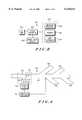
- a radio frequency identification stamp(“stamp") 10 is formed by printing on a first surface 12 of a substrate 24 indicia 14 indicative of at least a postage value.
- An antenna 16is formed on a second surface 18 and a radio frequency identification circuit chip (“circuit chip”) 20 is secured to second surface 18 and coupled to the antenna 16.
- a layer 22 of adhesiveshown in phantom in FIG. 2 to better illustrate antenna 16 and circuit chip 20, is also disposed on second surface 18.
- antenna 16is preferably formed on second surface 18 by printing using a conductive ink or other conductive medium, such as disclosed and described in the aforementioned and incorporated U.S. Patent Applications.
- Layer 22is deposited over substantially all of second surface 18, including antenna 16, bonding circuit chip 20 to second surface 18 and coupling circuit chip 20 to antenna 16.
- a preferred adhesiveis thus a conductive anisotropic adhesive designed to conduct only in a "z" direction (as indicated in FIG. 3).
- an isotropic adhesivemay be used if care is taken in the application of the isotropic adhesive to second surface 18 and in positioning circuit chip 20 to second surface 18.
- Layer 22is also used to releasably secure stamp 10 to a temporary backing (not shown) and to permanently secure stamp 10 to an envelope, an article or a package (not shown).
- stamp 10is a capacitive coupled device.
- Antenna 16includes a first antenna element 26 and a second antenna element 28.
- Circuit chip 20includes a first conductive pad and a second conductive pad (not shown) for coupling via adhesive layer 22 respectively to first antenna element 26 and second antenna element 28.
- stamp 10may be arranged as an inductive coupled device with a coil antenna and a suitable inductive coupled circuit chip.
- circuit chip 20may be coupled to antenna 16 using printing technology as shown in described in commonly assigned U.S. patent application, Attorney Docket No. IND10135, entitled “Radio Frequency Identification Tag Having Printed Circuit Interconnections", application number 09/115,279, filed Jul. 14, 1998, the disclosure of which is hereby expressly incorporated herein by reference.
- stamp 10may be arranged for read only operation or for read/write operation.
- a read only chipmay be used and contain stored information indicative of the fixed postage value.
- a preferred circuit chipis the Indala I341 circuit chip available from Motorola Indala Corporation, 3041 Orchard Parkway, San Jose, Calif. 95134.
- circuit chip 20will generate a read signal containing some or all of the stored information, for example, the postage value, and send a read signal containing the stored information to the base station.
- a mail sorting apparatuscan be adapted to distinguish envelopes, parcels and packages having sufficient postage without visual inspection of the stamp by detecting the read signal containing the postage value.
- stamp 10operate in a read/write manner.
- stamp 10may be advantageously constructed from a TEMIC e5550 circuit chip available from Temic North America, Inc., Basking Ridge, N.J.
- Circuit chip 20may contain preprogrammed stored information, such as standard postage values, and/or may, in a read/write embodiment, have information communicated to it and retained as stored information.
- a postage metercan be adapted to both print stamp 10 and to write data to circuit chip 20 as stored information via a data signal.
- a data signal containing the stored informationis communicated to stamp 10 and hence to circuit chip 20, which receives the data signal and retains the information as stored information.
- a sorting apparatus 100for sorting for example mail and/or other parcels or packages, includes an exciter/reader station 102, a conveyor 104 including a plurality of diverter paths, each of which is generally indicated as 106.
- exciter/reader station 102provides an exciter signal 112, such as an electrostatic excitation signal, as package 108 enters identification zone 110.
- Package 108such as an envelope, parcel or package, includes a stamp 10, and stamp 10 becomes energized in the presence of exciter signal 112.
- stamp 10generates a read signal 114 containing some or all of the stored information.
- the read signalcontains at least one of a postage value and a zip code.
- Sorting apparatus 100also includes a controller 101 coupled to exciter/reader station 102, to which the read signal is communicated. From the read signal, controller 101 may determine if sufficient postage value is present and, if a zip code is programmed, direct package 108 along one of the diverter paths 106 accordingly by sending a signal to a diverter controller (not shown). Additionally, sorting apparatus 100 may be adapted to provide a data signal 116 to stamp 10. Data signal 116 may contain additional stored information to be retained in circuit chip 20, such as additional tracking and routing information, and may also provide data canceling the postage value, i.e., canceling stamp 10. Each of the forgoing operations may be accomplished as package 108 is conducted through the sorting apparatus 100 and without visually inspecting or accessing stamp 10 and without visually referencing a printed bar code.
- stamp 210in accordance with alternate preferred embodiment of the present invention is shown in cross-section.
- Stamp 210is formed by printing on a first surface 212 of a substrate 224 indicia (not shown) indicative of at least a postage value.
- An antenna 216is formed on a second surface 218.
- Second surface 218is further formed with a recess 226 as a localized depression of substrate 224.
- a radio frequency identification circuit chip (“circuit chip”) 220is disposed within recess 226 and is secured to second surface 218 and coupled to the antenna 216.
- a layer 222 of adhesiveis also disposed on second surface 218.
- antenna 216is preferably formed on second surface 218 by printing using a conductive ink or other conductive medium and includes a first coupling region 228 and a second coupling region 230 extending into recess 226.
- Layer 222is deposited over substantially all of second surface 218, including antenna 216, and particularly first coupling region 228 and second coupling region 230, bonding circuit chip 20 to second surface 218 and coupling circuit chip 220 to antenna 216.
- a preferred adhesiveis thus a conductive anisotropic adhesive.
- An isotropic adhesivemay be used if care is taken in the application of the isotropic adhesive to second surface 218 and in positioning circuit chip 220 to second surface 218.
- Layer 222is also used to releasably secure stamp 210 to a temporary backing (not shown) and to permanently secure stamp 210 to an envelope, an article or a package (not shown).
- stamp 310is formed by printing on a first surface 312 of a substrate 324 indicia (not shown) indicative of at least a postage value.
- An antenna 316is formed on a second surface 318.
- Substrate 324forms a first layer of a laminate, and at least a second layer 332 is disposed over substrate 324 and is bonded to second surface 318 and antenna 316.
- Second layer 332includes an aperture 334 into which a radio frequency identification circuit chip (“circuit chip”) 320 is disposed and is secured to second surface 318 and coupled to antenna 316.
- a layer 336 of adhesiveis disposed over a surface 335 of second layer 332 and also covering circuit chip 320.
- antenna 316is preferably formed on second surface 318 by printing using a conductive ink or other conductive medium and includes a first coupling region 328 and a second coupling region 330 accessible within aperture 334.
- Circuit chip 320is bonded using a suitable conductive adhesive to second surface 318 within aperture 334 and is coupled to antenna 316 via first coupling region 328 and second coupling region 330.
- layer 336is applied over surface 335 and covering circuit chip 320.
- Layer 336is used to releasably secure stamp 310 to a temporary backing (not shown) and to permanently secure stamp 310 to an envelope, an article or a package (not shown).
- a package of radio frequency identification stamps(“package”) 400 includes a plurality of radio frequency identification stamps (one of which is shown as 410) releasably bonded to a backing 438.
- stamps 410are constructed in accordance with the present invention as described in terms of the several preferred embodiments, and are further preferably pre-programmed with a fixed postage value.
- Package 400provides a convenient way of selling radio frequency identification stamps of fixed value in bulk. Of course, it will be appreciated that package 400 may be in roll, booklet, sheet or any other suitable form without departing from the fair scope of the invention.
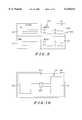
- an apparatus 500 for printing and programming radio frequency identification stampsin accordance with preferred embodiments of the present invention includes a user interface 502, a controller 504 and a printer/programming station 506.
- User interface 502allows a user to input to controller 504 a desired postage value for a radio frequency identification stamp and to instruct controller 504 to print the desired stamp.
- Controller 504includes a memory (not shown) in which purchased postage value is retained, and if sufficient purchased postage is available, causes printer/programming station 506 to generate the desired stamp.
- Controller 504may also be coupled, for example via a modem, to a remote postage value update facility 508 where additional postage value may be purchased. Upon purchasing postage value, either by facility 508 or otherwise, the memory within controller 504 is updated with the information relating to the available postage value.
- User interface 502may also include a scale and provide for calculating postage value, which upon authorization by the user to print the desired stamp, is communicated to controller 504. Additionally, the user may also input a zip code and potentially other delivery information such as a complete address via user interface 502.
- Printing/programming station 506includes a substrate transport 510, a printer 512 and a circuit chip programmer 514. Substrate transport 510 is arranged to conduct blank or preprinted substrate (not shown) through printer/programming station 506, and printer 512 is arranged to print indicia on the substrate. For example the indicia may be indicative of a postage value. In this regard, printer/programming station 506 is comparable to commercially available postage meter devices.
- Printer/programming station 506further includes circuit chip programmer 514, and the substrate is formed as described with respect to the various of the preferred embodiments of the present invention to include an antenna, a circuit chip coupled to the antenna and an adhesive layer.
- Circuit chip programmeris arranged to provide at least an exciter signal and a data signal to the substrate being printed via suitable antenna.
- the circuit chipbecomes energized in the presence of the exciter signal.
- the circuit chipfurther receives and acts upon the data signal.
- the data signalpreferably contains at least one of a postage value and a zip code, but may as described, contain additional delivery information.
- the information contained in the data signalis retained within the circuit chip as stored information, and the completed stamp is ejected from printer/programming station 506. The user then attaches the stamp using the adhesive layer to an envelope or package and mails it in the ordinary fashion.
- Radio frequency identification stampis extended to a radio frequency identification mailing label 600 ("mailing label").
- Mailing label 600is formed by printing on a first surface 612 of a substrate 624 indicia 614 indicative of delivery information.
- Delivery informationmay include sender information 601, recipient information 602, delivery service information 603 and billing instruction 604.
- An antenna 616is formed on a second surface 618 and a radio frequency identification circuit chip (“circuit chip") 620 is secured to second surface 618 and coupled to the antenna 616.
- a layer 622 of adhesiveshown in phantom in FIG. 10 to better illustrate antenna 616 and circuit chip 620, is also disposed on second surface 618.
- antenna 616is preferably formed on second surface 618 by printing using a conductive ink or other conductive medium, such as disclosed and described in the aforementioned and incorporated U.S. patent applications.
- Layer 622is deposited over substantially all of second surface 618, including antenna 616, bonding circuit chip 620 to second surface 618 and coupling circuit chip 620 to antenna 616.
- a preferred adhesiveis thus a conductive anisotropic adhesive designed to conduct in a single direction.
- an isotropic adhesivemay be used if care is taken in the application of the isotropic adhesive to second surface 618 and in positioning circuit chip 620 to second surface 618.
- Layer 622is also used to releasably secure mailing label 600 to a temporary backing (not shown) and to permanently secure mailing label 600 to an envelope, an article or a package (not shown).
- mailing label 600is a capacitive coupled device.
- Antenna 616includes a first antenna element 626 and a second antenna element 628.
- Circuit chip 620includes a first conductive pad and a second conductive pad (not shown) for coupling via adhesive layer 622 respectively to first antenna element 626 and second antenna element 628.
- mailing label 600may be arranged as an inductive coupled device with a coil antenna and a suitable inductive coupled circuit chip.
- circuit chip 620may be coupled to antenna 616 using printing technology as shown in described in the aforementioned commonly assigned U.S. patent application, Attorney Docket No.
- substrate 624may be formed with a recessed portion for receiving circuit chip 620 and/or a laminate structure having an aperture for receiving circuit chip 620.
- mailing label 600may be arranged for read only operation or for read/write operation.
- a read only chipmay be used and contain stored information including an article tracking number.
- a preferred circuit chipis the Indala 1341 circuit chip available from Motorola Indala Corporation, 3041 Orchard Parkway, San Jose, Calif. 95134.
- circuit chip 620will generate a read signal containing some or all of the stored information, for example, the tracking number, and send the read signal containing the stored information to the base station.
- a delivery person upon receipt of the packagemay manually enter the deliver information into a central database associating the delivery information with the tracking number. It will be appreciated that the article sorting apparatus described above with respect to FIG. 4 may be easily adapted for sorting articles based upon the tracking number and information contained in the central database.
- circuit chip 620may be advantageously constructed from a TEMIC e5550 circuit chip available from Temic North America, Inc., Basking Ridge, N.J. Circuit chip 620 may contain preprogrammed stored information, such as a tracking number, customer account number, and the like and/or may, in the read/write embodiment, have information communicated to it and retained as stored information.
- a label printing apparatusmay be adapted to both print indicia 614 on first surface 612 and to program circuit chip 620. Circuit chip 620 may then be programmed to contain such information as sender, recipient address, delivery service type and billing information.
- circuit chip 620may then be read from circuit chip 620 during article sorting operations permitting automated sorting and automated billing. For example, once mailing label 600 is prepared and circuit chip 620 is programmed, the stored information may be read throughout the delivery operation for routing the associated package to its proper destination. Additionally, upon delivery, the billing instruction is read and the appropriate party invoiced for the services. Should delivery instructions change, circuit chip 620 may be easily reprogrammed with the new delivery information using the same procedures.
- a radio frequency identification stamp 10includes a substrate 24 with a first surface 12 and a second surface 18.
- the first surface 12is printed with indicia indicating at least a postage value.
- An antenna 16is formed on the second surface 18 and a radio frequency identification circuit chip 20 is secured to the second surface 18 and coupled to the antenna 16.
- a layer of adhesive 22is also disposed on the second surface 18.
- a recess 226is formed in a second surface 218 and the circuit chip 220 is disposed within the recess 226.
- the substrate 324is a laminate wherein substrate 324 forms a first layer and the laminate includes at least a second layer 332. At least one of the substrate 324 and the second layer 332 is formed with an aperture 326, and the circuit chip 320 is disposed within the aperture 326 and is secured to the other of the substrate 324 and the second layer 332 and coupled to an antenna 316.
- a sorting apparatus 100includes an exciter/reader station 102 adjacent an identification zone 110 along a conveyor 104 including a plurality of diverter paths 106.
- Exciter/reader station 102is arranged to provide an exciter signal 112, such as an electrostatic excitation signal, as package 108 enters identification zone 110.
- Package 108such as an envelope, parcel or package, includes a stamp 10, and stamp 10 becomes energized in the presence of exciter signal 112 and generates a read signal 114 containing some or all of the stored information.
- Sorting apparatus 100also includes a controller 101 coupled to exciter/reader station 102, to which the read signal is communicated, and the controller 101 determines if a proper postage value is present and, if a zip code is programmed, directs package 108 along one of the diverter paths 106 accordingly.
- sorting apparatus 100may be adapted to provide a data signal 116 to stamp 10.
- the data signalmay contain additional stored information to be retained in circuit chip 20, such as additional tracking and routing information, and may also provide data canceling the postage value, i.e., canceling stamp 10.
- a stamp printer/programmerincludes a user interface 502, a controller 504 and a printer/programming station 506. Data is received from user interface 502 and controller directs printer/programming station 506 to generate a radio frequency identification stamp having printed indicia and a programmed circuit chip.
- the usermay input a postage value or a postage value may be automatically calculated, in addition a user may enter at least a zip code and potentially delivery address information.
- a substrate transport 510 within printer/programming station 506advances a blank substrate to printer 512, which prints the appropriate indicia.
- the printed substrateis advanced to the circuit chip programmer and an exciter signal and data signal are communicated to the substrate and energizing the circuit chip.
- the circuit chipreceives the data signal and retains, as appropriate, the stored information.
- a radio frequency identification mailing label 600includes indicia 614 printed on a first surface, and an antenna 616 coupled to a radio frequency identification circuit chip 620 disposed on a second surface 618.
- a layer 622 of adhesivecovers the second surface including the antenna 616. The layer bonds the circuit chip 620 to the second surface and couples the circuit chip 620 to the antenna 616.
- the circuit chip 620may retain a tracking number, and more preferably, retains sender information 601, recipient information 602, service type information 603 and billing instructions 604.
Landscapes
- Engineering & Computer Science (AREA)
- Microelectronics & Electronic Packaging (AREA)
- Computer Hardware Design (AREA)
- Physics & Mathematics (AREA)
- General Physics & Mathematics (AREA)
- Theoretical Computer Science (AREA)
- Power Engineering (AREA)
- Mechanical Engineering (AREA)
- Computer Networks & Wireless Communication (AREA)
- Condensed Matter Physics & Semiconductors (AREA)
- Discharge Of Articles From Conveyors (AREA)
- Sorting Of Articles (AREA)
Abstract
Description
Claims (24)
Priority Applications (3)
| Application Number | Priority Date | Filing Date | Title |
|---|---|---|---|
| US09/152,202US6130613A (en) | 1998-06-09 | 1998-09-11 | Radio frequency indentification stamp and radio frequency indentification mailing label |
| PCT/US1999/020310WO2000016278A1 (en) | 1998-09-11 | 1999-09-03 | Radio frequency identification stamp and radio frequency identification mailing label |
| EP99944080AEP1110190A4 (en) | 1998-09-11 | 1999-09-03 | Radio frequency identification stamp and radio frequency identification mailing label |
Applications Claiming Priority (3)
| Application Number | Priority Date | Filing Date | Title |
|---|---|---|---|
| US09/094,261US6107920A (en) | 1998-06-09 | 1998-06-09 | Radio frequency identification tag having an article integrated antenna |
| US09/103,226US6018299A (en) | 1998-06-09 | 1998-06-23 | Radio frequency identification tag having a printed antenna and method |
| US09/152,202US6130613A (en) | 1998-06-09 | 1998-09-11 | Radio frequency indentification stamp and radio frequency indentification mailing label |
Related Parent Applications (2)
| Application Number | Title | Priority Date | Filing Date |
|---|---|---|---|
| US09/094,261Continuation-In-PartUS6107920A (en) | 1998-06-09 | 1998-06-09 | Radio frequency identification tag having an article integrated antenna |
| US09/103,226Continuation-In-PartUS6018299A (en) | 1998-06-09 | 1998-06-23 | Radio frequency identification tag having a printed antenna and method |
Publications (1)
| Publication Number | Publication Date |
|---|---|
| US6130613Atrue US6130613A (en) | 2000-10-10 |
Family
ID=22541917
Family Applications (1)
| Application Number | Title | Priority Date | Filing Date |
|---|---|---|---|
| US09/152,202Expired - LifetimeUS6130613A (en) | 1998-06-09 | 1998-09-11 | Radio frequency indentification stamp and radio frequency indentification mailing label |
Country Status (3)
| Country | Link |
|---|---|
| US (1) | US6130613A (en) |
| EP (1) | EP1110190A4 (en) |
| WO (1) | WO2000016278A1 (en) |
Cited By (83)
| Publication number | Priority date | Publication date | Assignee | Title |
|---|---|---|---|---|
| US20020032435A1 (en)* | 2000-06-20 | 2002-03-14 | Levin Bruce H. | Tracking surgical implements with integrated circuits |
| US6384727B1 (en) | 2000-08-02 | 2002-05-07 | Motorola, Inc. | Capacitively powered radio frequency identification device |
| US6415336B1 (en)* | 1999-01-25 | 2002-07-02 | Pitney Bowes Inc. | Electronic indicium and methods of using same in postal processes |
| US6451154B1 (en)* | 2000-02-18 | 2002-09-17 | Moore North America, Inc. | RFID manufacturing concepts |
| US20020145036A1 (en)* | 2001-04-04 | 2002-10-10 | Otto Jerome A. | Radio frequency identification system and method |
| US20030030539A1 (en)* | 2001-08-07 | 2003-02-13 | Mcgarry Patrick J. | Vending audit system |
| US20030063139A1 (en)* | 2001-10-01 | 2003-04-03 | Hohberger Clive P. | Method and apparatus for associating on demand certain selected media and value-adding elements |
| US20030080182A1 (en)* | 2001-10-25 | 2003-05-01 | Gunther William G. | Distribution based postage tracking system and method |
| US20030111542A1 (en)* | 2001-12-19 | 2003-06-19 | 3M Innovative Properties Company | Article with retroreflective and radio frequency-responsive features |
| US6593853B1 (en)* | 2000-02-18 | 2003-07-15 | Brady Worldwide, Inc. | RFID label printing system |
| US6602374B2 (en)* | 2000-12-08 | 2003-08-05 | George Schmitt & Company, Inc. | System and method for creating coil of stamps with inner security strip |
| US20030197064A1 (en)* | 2002-04-19 | 2003-10-23 | Avery Dennison Corporation | Laser imageable RFID label/tag |
| US20030214388A1 (en)* | 2002-05-20 | 2003-11-20 | Stuart James Riley | RFID deployment system |
| US6667092B1 (en) | 2002-09-26 | 2003-12-23 | International Paper Company | RFID enabled corrugated structures |
| US20040049471A1 (en)* | 2002-09-10 | 2004-03-11 | Pitney Bowes Incorporated | Method for processing and delivering registered mail |
| US20040070504A1 (en)* | 2002-10-14 | 2004-04-15 | Brollier Brian W. | Semi-covert RFID enabled containers |
| US20040102870A1 (en)* | 2002-11-26 | 2004-05-27 | Andersen Scott Paul | RFID enabled paper rolls and system and method for tracking inventory |
| US20040122776A1 (en)* | 2002-12-18 | 2004-06-24 | Pitney Bowes Incorporated | Method for obtaining refunds from a meter that produces a dual postal indicia |
| US20040128264A1 (en)* | 2002-12-30 | 2004-07-01 | Pitney Bowes Inc. | Personal funds metering system and method |
| US20040243522A1 (en)* | 2003-05-29 | 2004-12-02 | Pitney Bowes Incorporated | Preregistered tracking labels |
| EP1519324A2 (en) | 2003-09-29 | 2005-03-30 | Pitney Bowes, Inc. | Method for postage evidencing for the payment of terminal dues |
| US20050071289A1 (en)* | 2003-09-29 | 2005-03-31 | Pitney Bowes Incorporated | Method for postage evidencing for the payment of terminal dues |
| US20050067486A1 (en)* | 2003-09-29 | 2005-03-31 | Pitney Bowes Incorporated | Method for postage evidencing for the payment of terminal dues using radio frequency identification tags |
| US20050071288A1 (en)* | 2003-09-29 | 2005-03-31 | Pitney Bowes Incorporated | Integrated payment for international business reply mail |
| US20050071293A1 (en)* | 2003-09-29 | 2005-03-31 | Pitney Bowes Incorporated | Method for postage evidencing with cross-border mail tracking capability and near real time for teminal dues reconcilation |
| US20050091821A1 (en)* | 2003-11-03 | 2005-05-05 | Best Scott D. | Method of manufacturing an article having a radio frequency identification (RFID) device |
| US20050131397A1 (en)* | 2001-03-30 | 2005-06-16 | Levin Bruce H. | Tracking surgical implements with integrated circuits |
| US20050131842A1 (en)* | 2003-12-10 | 2005-06-16 | Pitney Bowes Incorporated | Method for indicating the prepayment of customs duties |
| US20050131843A1 (en)* | 2003-12-10 | 2005-06-16 | Pitney Bowes Incorporated | Method for the prepayment of customs duties |
| US20050199724A1 (en)* | 2004-03-01 | 2005-09-15 | Allen Lubow | Diffractive optical variable image including barcode |
| US20050273434A1 (en)* | 2004-04-18 | 2005-12-08 | Allen Lubow | System and method for managing security in a supply chain |
| US20050270160A1 (en)* | 2004-06-04 | 2005-12-08 | Maines Paper And Food Service, Inc. | Radio frequency device for tracking goods |
| US20050284941A1 (en)* | 2004-06-28 | 2005-12-29 | Allen Lubow | Combined electromagnetic and optical communication system |
| US20060022824A1 (en)* | 2004-08-02 | 2006-02-02 | United Parcel Service Of America, Inc. | Systems and methods for using radio frequency identification tags to communicating sorting information |
| US20060036346A1 (en)* | 2002-11-26 | 2006-02-16 | Andersen Scott P | System and method for tracking inventory |
| US20060055014A1 (en)* | 2004-09-14 | 2006-03-16 | Semiconductor Energy Laboratory Co., Ltd. | Wireless chip and manufacturing method of the same |
| US20060055539A1 (en)* | 2004-09-09 | 2006-03-16 | Lawrence Daniel P | Antennas for radio frequency identification tags in the form of a logo, brand name, trademark, or the like |
| US20060082446A1 (en)* | 2004-10-08 | 2006-04-20 | Illinois Tools Works, Inc. | Label applicator system |
| US20060173798A1 (en)* | 2005-01-31 | 2006-08-03 | Pascal Charroppin | Method of providing tracking numbers for a mail piece |
| US20060186204A1 (en)* | 2004-06-28 | 2006-08-24 | International Barcode Corporation | Combined multi-frequency electromagnetic and optical communication system |
| US20060202269A1 (en)* | 2005-03-08 | 2006-09-14 | Semiconductor Energy Laboratory Co., Ltd. | Wireless chip and electronic appliance having the same |
| US20060213819A1 (en)* | 2000-12-01 | 2006-09-28 | United States Postal Service | System and method for directly connecting an advanced facer canceler system to a delivery bar code sorter |
| US7137000B2 (en) | 2001-08-24 | 2006-11-14 | Zih Corp. | Method and apparatus for article authentication |
| US7138919B2 (en) | 2004-02-23 | 2006-11-21 | Checkpoint Systems, Inc. | Identification marking and method for applying the identification marking to an item |
| US20070040684A1 (en)* | 2005-08-19 | 2007-02-22 | Mcallister Clarke W | Systems, methods, and devices for converting and commissioning wireless sensors |
| US20070115131A1 (en)* | 2003-11-25 | 2007-05-24 | Ntn Corporation | Bearing with ic tag and seal for the same |
| US20070187496A1 (en)* | 2006-02-10 | 2007-08-16 | Andersen Scott P | Inventory tracking system and method |
| US20070247287A1 (en)* | 2006-04-10 | 2007-10-25 | Dell Products L.P. | Method and apparatus for programming a transponder |
| US20080018431A1 (en)* | 2004-02-06 | 2008-01-24 | Turner Christopher G G | Rfid Group Selection Method |
| US20080034901A1 (en)* | 2002-09-30 | 2008-02-14 | Pitney Bowes Inc. | Hazardous material detector for detecting hazardous material in a mailstream |
| US20080068637A1 (en)* | 2006-09-15 | 2008-03-20 | Avery Levy | System and method for enabling transactions by means of print media that incorporate electronic recording and transmission means |
| US20080088448A1 (en)* | 2006-06-30 | 2008-04-17 | Steidinger David J | Method of making an rfid article |
| US7361251B2 (en) | 2002-01-18 | 2008-04-22 | Avery Dennison Corporation | RFID label technique |
| US20080272885A1 (en)* | 2004-01-22 | 2008-11-06 | Mikoh Corporation | Modular Radio Frequency Identification Tagging Method |
| US7457760B1 (en)* | 2008-02-25 | 2008-11-25 | International Business Machines Corporation | Programmable radio-frequency identification (RFID) postage stamps |
| US20080315311A1 (en)* | 2007-06-22 | 2008-12-25 | Semiconductor Energy Laboratory Co., Ltd. | Semiconductor device |
| US20090058609A1 (en)* | 2007-09-05 | 2009-03-05 | Clayman Henry M | Coupon provided with rfid tag and method of using the same |
| US7534045B2 (en) | 2003-11-25 | 2009-05-19 | Ntn Corporation | Bearing with IC tag and seal for the same |
| US7619520B2 (en) | 2005-01-14 | 2009-11-17 | William Berson | Radio frequency identification labels and systems and methods for making the same |
| US7621451B2 (en) | 2005-01-14 | 2009-11-24 | William Berson | Radio frequency identification labels and systems and methods for making the same |
| US7623034B2 (en) | 2005-04-25 | 2009-11-24 | Avery Dennison Corporation | High-speed RFID circuit placement method and device |
| US20090314829A1 (en)* | 2007-05-22 | 2009-12-24 | Mcallistor Clarke | Systems, Methods, and Devices for Replication of Data onto Wireless Sensors |
| US7651031B2 (en) | 2004-10-25 | 2010-01-26 | William Berson | Systems and methods for reading indicium |
| US20100036777A1 (en)* | 2008-08-07 | 2010-02-11 | Ebay Inc. | Method and system for postal payments and addressing |
| US7728726B2 (en)* | 2005-01-14 | 2010-06-01 | William Berson | Radio frequency identification labels |
| US20100156768A1 (en)* | 2008-12-22 | 2010-06-24 | Fletcher Ii James Douglas | Display media, method of forming display media, and printer for printing on display media |
| US20100250418A1 (en)* | 2009-03-30 | 2010-09-30 | Bank Of America Corporation | Rejected checks envelope and process |
| US20100245190A1 (en)* | 2004-09-03 | 2010-09-30 | Semiconductor Energy Laboratory Co., Ltd. | Heatlth data collecting system and semiconductor device |
| US20100283584A1 (en)* | 2005-08-19 | 2010-11-11 | Mcallister Clarke William | Systems, Methods, and Devices for Commissioning Wireless Sensors. |
| US7931413B2 (en) | 2005-01-14 | 2011-04-26 | William Berson | Printing system ribbon including print transferable circuitry and elements |
| US8408602B2 (en) | 2004-04-14 | 2013-04-02 | William Berson | Label for receiving indicia having variable spectral emissivity values |
| USRE44220E1 (en) | 1998-06-18 | 2013-05-14 | Zih Corp. | Electronic identification system and method with source authenticity |
| US8843231B2 (en) | 2011-09-13 | 2014-09-23 | United Parcel Service Of America, Inc. | Sort systems and methods |
| US9256773B2 (en) | 2011-07-27 | 2016-02-09 | Féinics Amatech Teoranta | Capacitive coupling of an RFID tag with a touch screen device acting as a reader |
| US9272805B2 (en) | 2005-08-19 | 2016-03-01 | Adasa Inc. | Systems, methods, and devices for commissioning wireless sensors |
| US9747480B2 (en) | 2011-12-05 | 2017-08-29 | Adasa Inc. | RFID and robots for multichannel shopping |
| US9780435B2 (en) | 2011-12-05 | 2017-10-03 | Adasa Inc. | Aerial inventory antenna |
| US9878825B1 (en) | 2015-06-02 | 2018-01-30 | Ecoenvelopes, Llc | Reusable top flap envelope with dual opposing seal flaps |
| US10050330B2 (en) | 2011-12-05 | 2018-08-14 | Adasa Inc. | Aerial inventory antenna |
| US10476130B2 (en) | 2011-12-05 | 2019-11-12 | Adasa Inc. | Aerial inventory antenna |
| US10471478B2 (en) | 2017-04-28 | 2019-11-12 | United Parcel Service Of America, Inc. | Conveyor belt assembly for identifying an asset sort location and methods of utilizing the same |
| US10846497B2 (en) | 2011-12-05 | 2020-11-24 | Adasa Inc. | Holonomic RFID reader |
| US11093722B2 (en) | 2011-12-05 | 2021-08-17 | Adasa Inc. | Holonomic RFID reader |
Families Citing this family (15)
| Publication number | Priority date | Publication date | Assignee | Title |
|---|---|---|---|---|
| FR2805916A1 (en)* | 2000-03-03 | 2001-09-07 | Robert Tan | Postage stamp with an electronic chip to aid sorting, uses stamp printed with location information and with spaces for printing of tariff and date, and carries integrated circuit on stamp |
| AU2001253581A1 (en)* | 2000-04-17 | 2001-10-30 | International Paper | Tax stamp authentication and product control |
| EP1168239A3 (en)* | 2000-06-21 | 2003-10-01 | PACHEM Papier - Chem. Produktions Gesellschaft m.b.H. & Co. KG | Adhesive label |
| DE10054831A1 (en)* | 2000-11-04 | 2002-05-08 | Bundesdruckerei Gmbh | Electronic tag system for individual- and mass-identification of piece-goods e.g. for automatic postal reception and delivery, uses electronic marker having at least one data-store and antenna |
| FR2827986B1 (en)* | 2001-07-30 | 2004-04-02 | Arjo Wiggins Sa | METHOD OF MANUFACTURING AN ARTICLE INCLUDING A FIBROUS LAYER AND AT LEAST ONE ELECTRONIC CHIP, AND ARTICLE THUS OBTAINED |
| US6701217B1 (en) | 2002-09-27 | 2004-03-02 | Pitney Bowes Inc. | Dual metering method for indicating the contents of mail |
| US20050137989A1 (en)* | 2003-12-19 | 2005-06-23 | Brookner George M. | Detecting copied value-added indicia |
| EP1842157A2 (en)* | 2005-01-14 | 2007-10-10 | William Berson | Radio frequency identification labels and systems and methods for making the same |
| WO2006081652A1 (en)* | 2005-02-07 | 2006-08-10 | Lyngsoe Systems Ltd. | Mail delivery tracking system and apparatus |
| DE102005025323A1 (en)* | 2005-05-31 | 2006-12-07 | Francotyp-Postalia Beteiligungs Ag | Information assigning method for mail item e.g. letter, involves temporally assigning electronic memory device to mail item and fetching information with partial information e.g. postage relevant parameter, into memory device |
| GB2433630A (en)* | 2005-12-22 | 2007-06-27 | Royal Mail Group Plc | Data hosting device with interfaced RFID tag |
| US20080265560A1 (en)* | 2007-04-27 | 2008-10-30 | Frances Todd Stewart | Postage stamp with stored information |
| WO2009004658A1 (en)* | 2007-07-03 | 2009-01-08 | Michele Carriero | Mailbox comprising a radio receiver for detecting stamps with a radio receiver, a detector for detecting letters with a dangerous content and a video camera |
| EP2679315B1 (en) | 2007-12-12 | 2016-11-09 | Alcatel Lucent | Postal package delivery system |
| IT1404257B1 (en)* | 2011-01-25 | 2013-11-15 | Defendini | METHOD OF STORING DATA IN A POSTED POSTAL PLATE |
Citations (11)
| Publication number | Priority date | Publication date | Assignee | Title |
|---|---|---|---|---|
| US3780368A (en)* | 1970-02-20 | 1973-12-18 | Svejsecentralen | Method of marking and subsequently localizing, identifying and recording physical objects |
| US5175418A (en)* | 1989-12-19 | 1992-12-29 | Sony Corporation | Information card system |
| DE4242992A1 (en)* | 1992-12-18 | 1994-06-23 | Esselte Meto Int Gmbh | Antitheft protection device for compact discs |
| US5497140A (en)* | 1992-08-12 | 1996-03-05 | Micron Technology, Inc. | Electrically powered postage stamp or mailing or shipping label operative with radio frequency (RF) communication |
| US5528222A (en)* | 1994-09-09 | 1996-06-18 | International Business Machines Corporation | Radio frequency circuit and memory in thin flexible package |
| US5566441A (en)* | 1993-03-11 | 1996-10-22 | British Technology Group Limited | Attaching an electronic circuit to a substrate |
| US5682143A (en)* | 1994-09-09 | 1997-10-28 | International Business Machines Corporation | Radio frequency identification tag |
| US5786626A (en)* | 1996-03-25 | 1998-07-28 | Ibm Corporation | Thin radio frequency transponder with leadframe antenna structure |
| US5847447A (en)* | 1996-07-09 | 1998-12-08 | Ambient Corporation | Capcitively coupled bi-directional data and power transmission system |
| US5854480A (en)* | 1995-07-18 | 1998-12-29 | Oki Electric Indusry Co., Ltd. | Tag with IC capacitively coupled to antenna |
| US6001211A (en)* | 1995-07-18 | 1999-12-14 | Oki Electric Industry Co., Ltd. | Method of producing a tag device with IC capacitively coupled to antenna |
Family Cites Families (4)
| Publication number | Priority date | Publication date | Assignee | Title |
|---|---|---|---|---|
| JP2814477B2 (en)* | 1995-04-13 | 1998-10-22 | ソニーケミカル株式会社 | Non-contact IC card and method of manufacturing the same |
| GB9601899D0 (en)* | 1996-01-31 | 1996-04-03 | Neopost Ltd | Mailing system |
| DE19701163C2 (en)* | 1997-01-15 | 2001-12-06 | Siemens Ag | Electrical circuit especially for a chip card |
| DE19732645A1 (en)* | 1997-07-29 | 1998-09-10 | Siemens Ag | Combination chip card manufacturing method |
- 1998
- 1998-09-11USUS09/152,202patent/US6130613A/ennot_activeExpired - Lifetime
- 1999
- 1999-09-03WOPCT/US1999/020310patent/WO2000016278A1/ennot_activeApplication Discontinuation
- 1999-09-03EPEP99944080Apatent/EP1110190A4/ennot_activeWithdrawn
Patent Citations (11)
| Publication number | Priority date | Publication date | Assignee | Title |
|---|---|---|---|---|
| US3780368A (en)* | 1970-02-20 | 1973-12-18 | Svejsecentralen | Method of marking and subsequently localizing, identifying and recording physical objects |
| US5175418A (en)* | 1989-12-19 | 1992-12-29 | Sony Corporation | Information card system |
| US5497140A (en)* | 1992-08-12 | 1996-03-05 | Micron Technology, Inc. | Electrically powered postage stamp or mailing or shipping label operative with radio frequency (RF) communication |
| DE4242992A1 (en)* | 1992-12-18 | 1994-06-23 | Esselte Meto Int Gmbh | Antitheft protection device for compact discs |
| US5566441A (en)* | 1993-03-11 | 1996-10-22 | British Technology Group Limited | Attaching an electronic circuit to a substrate |
| US5528222A (en)* | 1994-09-09 | 1996-06-18 | International Business Machines Corporation | Radio frequency circuit and memory in thin flexible package |
| US5682143A (en)* | 1994-09-09 | 1997-10-28 | International Business Machines Corporation | Radio frequency identification tag |
| US5854480A (en)* | 1995-07-18 | 1998-12-29 | Oki Electric Indusry Co., Ltd. | Tag with IC capacitively coupled to antenna |
| US6001211A (en)* | 1995-07-18 | 1999-12-14 | Oki Electric Industry Co., Ltd. | Method of producing a tag device with IC capacitively coupled to antenna |
| US5786626A (en)* | 1996-03-25 | 1998-07-28 | Ibm Corporation | Thin radio frequency transponder with leadframe antenna structure |
| US5847447A (en)* | 1996-07-09 | 1998-12-08 | Ambient Corporation | Capcitively coupled bi-directional data and power transmission system |
Cited By (143)
| Publication number | Priority date | Publication date | Assignee | Title |
|---|---|---|---|---|
| USRE44220E1 (en) | 1998-06-18 | 2013-05-14 | Zih Corp. | Electronic identification system and method with source authenticity |
| US6415336B1 (en)* | 1999-01-25 | 2002-07-02 | Pitney Bowes Inc. | Electronic indicium and methods of using same in postal processes |
| US6593853B1 (en)* | 2000-02-18 | 2003-07-15 | Brady Worldwide, Inc. | RFID label printing system |
| US6451154B1 (en)* | 2000-02-18 | 2002-09-17 | Moore North America, Inc. | RFID manufacturing concepts |
| US20020195195A1 (en)* | 2000-02-18 | 2002-12-26 | Moore North America, Inc.. | RFID manufacturing concepts |
| US20020195194A1 (en)* | 2000-02-18 | 2002-12-26 | Moore North America, Inc.. | RFID manufacturing concepts |
| US7045186B2 (en) | 2000-02-18 | 2006-05-16 | Moore North America, Inc. | RFID manufacturing concepts |
| US7014729B2 (en) | 2000-02-18 | 2006-03-21 | Moore Wallace North America, Inc. | RFID manufacturing concepts |
| US20020032435A1 (en)* | 2000-06-20 | 2002-03-14 | Levin Bruce H. | Tracking surgical implements with integrated circuits |
| US6384727B1 (en) | 2000-08-02 | 2002-05-07 | Motorola, Inc. | Capacitively powered radio frequency identification device |
| US20060213819A1 (en)* | 2000-12-01 | 2006-09-28 | United States Postal Service | System and method for directly connecting an advanced facer canceler system to a delivery bar code sorter |
| US6602374B2 (en)* | 2000-12-08 | 2003-08-05 | George Schmitt & Company, Inc. | System and method for creating coil of stamps with inner security strip |
| US9495632B2 (en) | 2001-02-02 | 2016-11-15 | Avery Dennison Corporation | RFID label technique |
| US20050131397A1 (en)* | 2001-03-30 | 2005-06-16 | Levin Bruce H. | Tracking surgical implements with integrated circuits |
| US7256696B2 (en) | 2001-03-30 | 2007-08-14 | Bruce Levin | Tracking surgical implements with integrated circuits |
| US20080007411A1 (en)* | 2001-03-30 | 2008-01-10 | Levin Bruce H | Tracking surgical implements with integrated circuits |
| US20020145036A1 (en)* | 2001-04-04 | 2002-10-10 | Otto Jerome A. | Radio frequency identification system and method |
| US6732923B2 (en) | 2001-04-04 | 2004-05-11 | Ncr Corporation | Radio frequency identification system and method |
| WO2003015039A3 (en)* | 2001-08-07 | 2003-05-22 | Mars Inc | Vending audit system |
| EP1419660A4 (en)* | 2001-08-07 | 2006-04-12 | Mars Inc | Vending audit system |
| US7053773B2 (en) | 2001-08-07 | 2006-05-30 | Mars Incorporated | Vending audit system |
| US20030030539A1 (en)* | 2001-08-07 | 2003-02-13 | Mcgarry Patrick J. | Vending audit system |
| US8667276B2 (en) | 2001-08-24 | 2014-03-04 | Zih Corp. | Method and apparatus for article authentication |
| US7137000B2 (en) | 2001-08-24 | 2006-11-14 | Zih Corp. | Method and apparatus for article authentication |
| US7664257B2 (en) | 2001-08-24 | 2010-02-16 | Zih Corp. | Method and apparatus for article authentication |
| US8301886B2 (en) | 2001-08-24 | 2012-10-30 | Zih Corp. | Method and apparatus for article authentication |
| US20030063139A1 (en)* | 2001-10-01 | 2003-04-03 | Hohberger Clive P. | Method and apparatus for associating on demand certain selected media and value-adding elements |
| US6857714B2 (en) | 2001-10-01 | 2005-02-22 | Zih Corp. | Method and apparatus for associating on demand certain selected media and value-adding elements |
| US6817517B2 (en) | 2001-10-25 | 2004-11-16 | George Schmitt & Company, Inc. | Distribution based postage tracking system and method |
| US20030080182A1 (en)* | 2001-10-25 | 2003-05-01 | Gunther William G. | Distribution based postage tracking system and method |
| US6758405B2 (en)* | 2001-12-19 | 2004-07-06 | 3M Innovative Properties Company | Article with retroreflective and radio frequency-responsive features |
| US20030111542A1 (en)* | 2001-12-19 | 2003-06-19 | 3M Innovative Properties Company | Article with retroreflective and radio frequency-responsive features |
| US7361251B2 (en) | 2002-01-18 | 2008-04-22 | Avery Dennison Corporation | RFID label technique |
| US8246773B2 (en) | 2002-01-18 | 2012-08-21 | Avery Dennison Corporation | RFID label technique |
| US7368032B2 (en) | 2002-01-18 | 2008-05-06 | Avery Dennison Corporation | RFID label technique |
| US6851617B2 (en)* | 2002-04-19 | 2005-02-08 | Avery Dennison Corporation | Laser imageable RFID label/tag |
| WO2003090151A3 (en)* | 2002-04-19 | 2003-12-04 | Avery Dennison Corp | Laser imageable rfid label/tag |
| US20030197064A1 (en)* | 2002-04-19 | 2003-10-23 | Avery Dennison Corporation | Laser imageable RFID label/tag |
| US20030214388A1 (en)* | 2002-05-20 | 2003-11-20 | Stuart James Riley | RFID deployment system |
| US20040049471A1 (en)* | 2002-09-10 | 2004-03-11 | Pitney Bowes Incorporated | Method for processing and delivering registered mail |
| US6667092B1 (en) | 2002-09-26 | 2003-12-23 | International Paper Company | RFID enabled corrugated structures |
| US7556250B2 (en)* | 2002-09-30 | 2009-07-07 | Pitney Bowes Inc. | Hazardous material detector for detecting hazardous material in a mailstream |
| US20080034901A1 (en)* | 2002-09-30 | 2008-02-14 | Pitney Bowes Inc. | Hazardous material detector for detecting hazardous material in a mailstream |
| US20040070504A1 (en)* | 2002-10-14 | 2004-04-15 | Brollier Brian W. | Semi-covert RFID enabled containers |
| US20060036346A1 (en)* | 2002-11-26 | 2006-02-16 | Andersen Scott P | System and method for tracking inventory |
| US7818088B2 (en) | 2002-11-26 | 2010-10-19 | Rush Tracking Systems, Llc | System and method for tracking inventory |
| US7151979B2 (en) | 2002-11-26 | 2006-12-19 | International Paper Company | System and method for tracking inventory |
| US8295974B2 (en) | 2002-11-26 | 2012-10-23 | Rush Tracking Systems, Llc | System and method for tracking inventory |
| US20110015780A1 (en)* | 2002-11-26 | 2011-01-20 | Scott Paul Andersen | System And Method For Tracking Inventory |
| US20040102870A1 (en)* | 2002-11-26 | 2004-05-27 | Andersen Scott Paul | RFID enabled paper rolls and system and method for tracking inventory |
| US8774960B2 (en) | 2002-11-26 | 2014-07-08 | Totaltrax, Inc. | System and method for tracking inventory |
| US20040122776A1 (en)* | 2002-12-18 | 2004-06-24 | Pitney Bowes Incorporated | Method for obtaining refunds from a meter that produces a dual postal indicia |
| US7840492B2 (en)* | 2002-12-30 | 2010-11-23 | Pitney Bowes Inc. | Personal funds metering system and method |
| US20040128264A1 (en)* | 2002-12-30 | 2004-07-01 | Pitney Bowes Inc. | Personal funds metering system and method |
| US20040243522A1 (en)* | 2003-05-29 | 2004-12-02 | Pitney Bowes Incorporated | Preregistered tracking labels |
| US7899758B2 (en)* | 2003-05-29 | 2011-03-01 | Pitney Bowes Inc. | Preregistered tracking labels |
| EP1519324A3 (en)* | 2003-09-29 | 2006-09-20 | Pitney Bowes, Inc. | Method for postage evidencing for the payment of terminal dues |
| EP1519324A2 (en) | 2003-09-29 | 2005-03-30 | Pitney Bowes, Inc. | Method for postage evidencing for the payment of terminal dues |
| US20050071289A1 (en)* | 2003-09-29 | 2005-03-31 | Pitney Bowes Incorporated | Method for postage evidencing for the payment of terminal dues |
| US7389274B2 (en) | 2003-09-29 | 2008-06-17 | Pitney Bowes Inc. | Integrated payment for international business reply mail |
| US20050067486A1 (en)* | 2003-09-29 | 2005-03-31 | Pitney Bowes Incorporated | Method for postage evidencing for the payment of terminal dues using radio frequency identification tags |
| US20050071288A1 (en)* | 2003-09-29 | 2005-03-31 | Pitney Bowes Incorporated | Integrated payment for international business reply mail |
| US8279064B2 (en)* | 2003-09-29 | 2012-10-02 | Pitney Bowes Inc. | Method for postage evidencing for the payment of terminal dues using radio frequency identification tags |
| US20050071293A1 (en)* | 2003-09-29 | 2005-03-31 | Pitney Bowes Incorporated | Method for postage evidencing with cross-border mail tracking capability and near real time for teminal dues reconcilation |
| US20050091821A1 (en)* | 2003-11-03 | 2005-05-05 | Best Scott D. | Method of manufacturing an article having a radio frequency identification (RFID) device |
| US7534045B2 (en) | 2003-11-25 | 2009-05-19 | Ntn Corporation | Bearing with IC tag and seal for the same |
| US7971792B2 (en) | 2003-11-25 | 2011-07-05 | Ntn Corporation | Bearing with IC tag and seal for the same |
| US20070115131A1 (en)* | 2003-11-25 | 2007-05-24 | Ntn Corporation | Bearing with ic tag and seal for the same |
| US20050131843A1 (en)* | 2003-12-10 | 2005-06-16 | Pitney Bowes Incorporated | Method for the prepayment of customs duties |
| US20050131842A1 (en)* | 2003-12-10 | 2005-06-16 | Pitney Bowes Incorporated | Method for indicating the prepayment of customs duties |
| US20080272885A1 (en)* | 2004-01-22 | 2008-11-06 | Mikoh Corporation | Modular Radio Frequency Identification Tagging Method |
| US8981909B2 (en) | 2004-02-06 | 2015-03-17 | Zih Corp. | RFID group selection method |
| US20080018431A1 (en)* | 2004-02-06 | 2008-01-24 | Turner Christopher G G | Rfid Group Selection Method |
| US7138919B2 (en) | 2004-02-23 | 2006-11-21 | Checkpoint Systems, Inc. | Identification marking and method for applying the identification marking to an item |
| US7267280B2 (en) | 2004-03-01 | 2007-09-11 | International Barcode Coporation | Diffractive optical variable image including barcode |
| US20050199724A1 (en)* | 2004-03-01 | 2005-09-15 | Allen Lubow | Diffractive optical variable image including barcode |
| US8408602B2 (en) | 2004-04-14 | 2013-04-02 | William Berson | Label for receiving indicia having variable spectral emissivity values |
| US9082322B2 (en) | 2004-04-14 | 2015-07-14 | William Berson | Label for receiving indicia having variable spectral emissivity values |
| US8684416B2 (en) | 2004-04-14 | 2014-04-01 | William Berson | Label for receiving indicia having variable spectral emissivity values |
| US20050273434A1 (en)* | 2004-04-18 | 2005-12-08 | Allen Lubow | System and method for managing security in a supply chain |
| US20050270160A1 (en)* | 2004-06-04 | 2005-12-08 | Maines Paper And Food Service, Inc. | Radio frequency device for tracking goods |
| US7142121B2 (en)* | 2004-06-04 | 2006-11-28 | Endicott Interconnect Technologies, Inc. | Radio frequency device for tracking goods |
| US7549591B2 (en) | 2004-06-28 | 2009-06-23 | International Barcode Corporation | Combined multi-frequency electromagnetic and optical communication system |
| US20050284941A1 (en)* | 2004-06-28 | 2005-12-29 | Allen Lubow | Combined electromagnetic and optical communication system |
| US7284704B2 (en) | 2004-06-28 | 2007-10-23 | International Barcode Corporation | Combined electromagnetic and optical communication system |
| US20060186204A1 (en)* | 2004-06-28 | 2006-08-24 | International Barcode Corporation | Combined multi-frequency electromagnetic and optical communication system |
| US7221276B2 (en)* | 2004-08-02 | 2007-05-22 | United Parcel Service Of America, Inc. | Systems and methods for using radio frequency identification tags to communicating sorting information |
| US20060022824A1 (en)* | 2004-08-02 | 2006-02-02 | United Parcel Service Of America, Inc. | Systems and methods for using radio frequency identification tags to communicating sorting information |
| US20100245190A1 (en)* | 2004-09-03 | 2010-09-30 | Semiconductor Energy Laboratory Co., Ltd. | Heatlth data collecting system and semiconductor device |
| US8547221B2 (en)* | 2004-09-03 | 2013-10-01 | Semiconductor Energy Laboratory Co., Ltd. | Health data collecting system and semiconductor device |
| US9450290B2 (en) | 2004-09-03 | 2016-09-20 | Semiconductor Energy Laboratory Co., Ltd. | Health data collecting system and semiconductor device |
| US20060055539A1 (en)* | 2004-09-09 | 2006-03-16 | Lawrence Daniel P | Antennas for radio frequency identification tags in the form of a logo, brand name, trademark, or the like |
| US8698262B2 (en) | 2004-09-14 | 2014-04-15 | Semiconductor Energy Laboratory Co., Ltd. | Wireless chip and manufacturing method of the same |
| US20060055014A1 (en)* | 2004-09-14 | 2006-03-16 | Semiconductor Energy Laboratory Co., Ltd. | Wireless chip and manufacturing method of the same |
| US20060082446A1 (en)* | 2004-10-08 | 2006-04-20 | Illinois Tools Works, Inc. | Label applicator system |
| US7193517B2 (en)* | 2004-10-08 | 2007-03-20 | Illinois Tool Works Inc. | Label applicator system |
| US8235298B2 (en) | 2004-10-25 | 2012-08-07 | William Berson | Systems and methods for reading indicium |
| US7651031B2 (en) | 2004-10-25 | 2010-01-26 | William Berson | Systems and methods for reading indicium |
| US7931413B2 (en) | 2005-01-14 | 2011-04-26 | William Berson | Printing system ribbon including print transferable circuitry and elements |
| US7728726B2 (en)* | 2005-01-14 | 2010-06-01 | William Berson | Radio frequency identification labels |
| US7619520B2 (en) | 2005-01-14 | 2009-11-17 | William Berson | Radio frequency identification labels and systems and methods for making the same |
| US8992105B2 (en) | 2005-01-14 | 2015-03-31 | William Berson | Printing system ribbon including print transferable circuitry and elements |
| US7621451B2 (en) | 2005-01-14 | 2009-11-24 | William Berson | Radio frequency identification labels and systems and methods for making the same |
| US20110227328A1 (en)* | 2005-01-14 | 2011-09-22 | William Berson | Radio frequency identification labels transfer printed from a ribbon |
| US20060173798A1 (en)* | 2005-01-31 | 2006-08-03 | Pascal Charroppin | Method of providing tracking numbers for a mail piece |
| US8455954B2 (en) | 2005-03-08 | 2013-06-04 | Semiconductor Energy Laboratory Co., Ltd. | Wireless chip and electronic appliance having the same |
| US20060202269A1 (en)* | 2005-03-08 | 2006-09-14 | Semiconductor Energy Laboratory Co., Ltd. | Wireless chip and electronic appliance having the same |
| US7623034B2 (en) | 2005-04-25 | 2009-11-24 | Avery Dennison Corporation | High-speed RFID circuit placement method and device |
| US8531297B2 (en) | 2005-04-25 | 2013-09-10 | Avery Dennison Corporation | High-speed RFID circuit placement method and device |
| US8228198B2 (en) | 2005-08-19 | 2012-07-24 | Adasa Inc. | Systems, methods, and devices for commissioning wireless sensors |
| US9272805B2 (en) | 2005-08-19 | 2016-03-01 | Adasa Inc. | Systems, methods, and devices for commissioning wireless sensors |
| US20070040684A1 (en)* | 2005-08-19 | 2007-02-22 | Mcallister Clarke W | Systems, methods, and devices for converting and commissioning wireless sensors |
| US7830258B2 (en)* | 2005-08-19 | 2010-11-09 | Adasa, Inc. | Systems, methods, and devices for converting and commissioning wireless sensors |
| US20100283584A1 (en)* | 2005-08-19 | 2010-11-11 | Mcallister Clarke William | Systems, Methods, and Devices for Commissioning Wireless Sensors. |
| US20070187496A1 (en)* | 2006-02-10 | 2007-08-16 | Andersen Scott P | Inventory tracking system and method |
| US7479870B2 (en)* | 2006-04-10 | 2009-01-20 | Dell Products L.P. | Method and apparatus for programming a transponder |
| US20070247287A1 (en)* | 2006-04-10 | 2007-10-25 | Dell Products L.P. | Method and apparatus for programming a transponder |
| US7901533B2 (en) | 2006-06-30 | 2011-03-08 | Tamarack Products, Inc. | Method of making an RFID article |
| US20080088448A1 (en)* | 2006-06-30 | 2008-04-17 | Steidinger David J | Method of making an rfid article |
| US8125667B2 (en) | 2006-09-15 | 2012-02-28 | Avery Levy | System and method for enabling transactions by means of print media that incorporate electronic recording and transmission means |
| US20080068637A1 (en)* | 2006-09-15 | 2008-03-20 | Avery Levy | System and method for enabling transactions by means of print media that incorporate electronic recording and transmission means |
| US8970864B2 (en) | 2006-09-15 | 2015-03-03 | Avery Levy | System and method for enabling transactions by means of print media that incorporate electronic recording and transmission means |
| US20090314829A1 (en)* | 2007-05-22 | 2009-12-24 | Mcallistor Clarke | Systems, Methods, and Devices for Replication of Data onto Wireless Sensors |
| US20080315311A1 (en)* | 2007-06-22 | 2008-12-25 | Semiconductor Energy Laboratory Co., Ltd. | Semiconductor device |
| US20090058609A1 (en)* | 2007-09-05 | 2009-03-05 | Clayman Henry M | Coupon provided with rfid tag and method of using the same |
| US7457760B1 (en)* | 2008-02-25 | 2008-11-25 | International Business Machines Corporation | Programmable radio-frequency identification (RFID) postage stamps |
| US20100036777A1 (en)* | 2008-08-07 | 2010-02-11 | Ebay Inc. | Method and system for postal payments and addressing |
| US20100156768A1 (en)* | 2008-12-22 | 2010-06-24 | Fletcher Ii James Douglas | Display media, method of forming display media, and printer for printing on display media |
| US20100250418A1 (en)* | 2009-03-30 | 2010-09-30 | Bank Of America Corporation | Rejected checks envelope and process |
| US8468074B2 (en)* | 2009-03-30 | 2013-06-18 | Bank Of America Corporation | Rejected checks envelope and process |
| US9256773B2 (en) | 2011-07-27 | 2016-02-09 | Féinics Amatech Teoranta | Capacitive coupling of an RFID tag with a touch screen device acting as a reader |
| US9043013B2 (en) | 2011-09-13 | 2015-05-26 | United Parcel Service Of America, Inc. | Sort systems and methods |
| US8843231B2 (en) | 2011-09-13 | 2014-09-23 | United Parcel Service Of America, Inc. | Sort systems and methods |
| US10846497B2 (en) | 2011-12-05 | 2020-11-24 | Adasa Inc. | Holonomic RFID reader |
| US9747480B2 (en) | 2011-12-05 | 2017-08-29 | Adasa Inc. | RFID and robots for multichannel shopping |
| US9780435B2 (en) | 2011-12-05 | 2017-10-03 | Adasa Inc. | Aerial inventory antenna |
| US10050330B2 (en) | 2011-12-05 | 2018-08-14 | Adasa Inc. | Aerial inventory antenna |
| US10476130B2 (en) | 2011-12-05 | 2019-11-12 | Adasa Inc. | Aerial inventory antenna |
| US11093722B2 (en) | 2011-12-05 | 2021-08-17 | Adasa Inc. | Holonomic RFID reader |
| US9878825B1 (en) | 2015-06-02 | 2018-01-30 | Ecoenvelopes, Llc | Reusable top flap envelope with dual opposing seal flaps |
| US10471478B2 (en) | 2017-04-28 | 2019-11-12 | United Parcel Service Of America, Inc. | Conveyor belt assembly for identifying an asset sort location and methods of utilizing the same |
| US11090689B2 (en) | 2017-04-28 | 2021-08-17 | United Parcel Service Of America, Inc. | Conveyor belt assembly for identifying an asset sort location and methods of utilizing the same |
| US11858010B2 (en) | 2017-04-28 | 2024-01-02 | United Parcel Service Of America, Inc. | Conveyor belt assembly for identifying an asset sort location and methods of utilizing the same |
Also Published As
| Publication number | Publication date |
|---|---|
| EP1110190A4 (en) | 2002-10-09 |
| WO2000016278A1 (en) | 2000-03-23 |
| EP1110190A1 (en) | 2001-06-27 |
Similar Documents
| Publication | Publication Date | Title |
|---|---|---|
| US6130613A (en) | Radio frequency indentification stamp and radio frequency indentification mailing label | |
| US5153842A (en) | Integrated circuit package label and/or manifest system | |
| US5684705A (en) | Mailing system | |
| EP1398735B1 (en) | Method for detecting and redirecting misdirected mail | |
| EP1022065B1 (en) | Electronic indicium and methods of using same in postal processes | |
| EP0999903B1 (en) | Improved package and mail delivery system | |
| CA2391768C (en) | System and method for verifying the delivery of a mailing and the material contained within the mailing | |
| US8132726B2 (en) | Postal stamp tracking system and method | |
| US6965866B2 (en) | Product warranty registration system and method | |
| US6738689B2 (en) | Method for detecting and redirecting major mailer's special service mail | |
| US7457760B1 (en) | Programmable radio-frequency identification (RFID) postage stamps | |
| EP0788075B1 (en) | Mailing system | |
| US20010037248A1 (en) | Product warranty registration system and method | |
| EP1687758B1 (en) | System for routing and tracking deliverables | |
| US20010032190A1 (en) | Identification mark for storing information, device for writing information on the mark, mark processing system, and associated methods | |
| JP4184483B2 (en) | Delivery slip issuing system | |
| GB2275668A (en) | Data carrying articles such as stamps | |
| EP1515279A1 (en) | Method for processing and delivering registered mail | |
| US20040049471A1 (en) | Method for processing and delivering registered mail | |
| JPH11213105A (en) | Reception device and reception method | |
| US20100206946A1 (en) | Method and device for accepting objects that are to be transported | |
| JP2002179220A (en) | Article delivery system and slip and automatic slip attaching device for article delivery system |
Legal Events
| Date | Code | Title | Description |
|---|---|---|---|
| AS | Assignment | Owner name:MOTOROLA, INC., ILLINOIS Free format text:ASSIGNMENT OF ASSIGNORS INTEREST;ASSIGNORS:EBERHART, NOEL H.;VEGA, VICTOR ALLEN;REYES, FERNANDO;REEL/FRAME:009459/0622;SIGNING DATES FROM 19980806 TO 19980810 | |
| STCF | Information on status: patent grant | Free format text:PATENTED CASE | |
| FPAY | Fee payment | Year of fee payment:4 | |
| FPAY | Fee payment | Year of fee payment:8 | |
| AS | Assignment | Owner name:MOTOROLA MOBILITY, INC, ILLINOIS Free format text:ASSIGNMENT OF ASSIGNORS INTEREST;ASSIGNOR:MOTOROLA, INC;REEL/FRAME:025673/0558 Effective date:20100731 | |
| FPAY | Fee payment | Year of fee payment:12 | |
| AS | Assignment | Owner name:MOTOROLA MOBILITY LLC, ILLINOIS Free format text:CHANGE OF NAME;ASSIGNOR:MOTOROLA MOBILITY, INC.;REEL/FRAME:029216/0282 Effective date:20120622 | |
| AS | Assignment | Owner name:GOOGLE TECHNOLOGY HOLDINGS LLC, CALIFORNIA Free format text:ASSIGNMENT OF ASSIGNORS INTEREST;ASSIGNOR:MOTOROLA MOBILITY LLC;REEL/FRAME:034237/0001 Effective date:20141028 |