US6127831A - Method of testing a semiconductor device by automatically measuring probe tip parameters - Google Patents
Method of testing a semiconductor device by automatically measuring probe tip parametersDownload PDFInfo
- Publication number
- US6127831A US6127831AUS08/844,577US84457797AUS6127831AUS 6127831 AUS6127831 AUS 6127831AUS 84457797 AUS84457797 AUS 84457797AUS 6127831 AUS6127831 AUS 6127831A
- Authority
- US
- United States
- Prior art keywords
- probe
- measuring
- probe tip
- testing
- tips
- Prior art date
- Legal status (The legal status is an assumption and is not a legal conclusion. Google has not performed a legal analysis and makes no representation as to the accuracy of the status listed.)
- Expired - Lifetime
Links
Images


Classifications
- G—PHYSICS
- G01—MEASURING; TESTING
- G01R—MEASURING ELECTRIC VARIABLES; MEASURING MAGNETIC VARIABLES
- G01R31/00—Arrangements for testing electric properties; Arrangements for locating electric faults; Arrangements for electrical testing characterised by what is being tested not provided for elsewhere
- G01R31/28—Testing of electronic circuits, e.g. by signal tracer
- G01R31/316—Testing of analog circuits
- G—PHYSICS
- G01—MEASURING; TESTING
- G01R—MEASURING ELECTRIC VARIABLES; MEASURING MAGNETIC VARIABLES
- G01R3/00—Apparatus or processes specially adapted for the manufacture or maintenance of measuring instruments, e.g. of probe tips
- G—PHYSICS
- G01—MEASURING; TESTING
- G01R—MEASURING ELECTRIC VARIABLES; MEASURING MAGNETIC VARIABLES
- G01R1/00—Details of instruments or arrangements of the types included in groups G01R5/00 - G01R13/00 and G01R31/00
- G01R1/02—General constructional details
- G01R1/06—Measuring leads; Measuring probes
- G01R1/067—Measuring probes
- G01R1/073—Multiple probes
- G01R1/07307—Multiple probes with individual probe elements, e.g. needles, cantilever beams or bump contacts, fixed in relation to each other, e.g. bed of nails fixture or probe card
- G01R1/07342—Multiple probes with individual probe elements, e.g. needles, cantilever beams or bump contacts, fixed in relation to each other, e.g. bed of nails fixture or probe card the body of the probe being at an angle other than perpendicular to test object, e.g. probe card
Definitions
- the present inventiongenerally relates to testing semiconductor devices, and more specifically to a method of testing semiconductor devices that includes automatically measuring and adjusting probe tip parameters including spring tension and electrical resistance.
- probeOne of the steps in the manufacturing of integrated circuits is called "probe". After the finished processing of a wafer, the wafer has to be tested with a probe card at a prober station in order to electrically test the performance of each die before it is packaged. At this point, die that fail in probe are marked as defective and ultimately discarded. A die can fail for a number of reasons. One such cause of failure could be due to hardware failure, when the die in fact could be perfectly good.
- a proberprovides a means for a die in a wafer to make electrical contact with a probe card which is connected to test hardware.
- probe cardshave a number of probe tips that contact either bond pads peripherally or bumps in array form on a die. It is often necessary for the probe tips to scrape an oxidation layer off the bond pad or bump in order to make electrical contact. This requires a certain probe tip force and an X and/or Y motion.
- probe cardsWith today's level of integration, dies and corresponding probe cards need to make a large number of contacts. Several hundred simultaneous contact are not uncommon. One result is that probe cards contain large numbers of probe tips, each of which must make contact with the corresponding target peripheral bond pads or array bumps. Unfortunately however, it is possible that different probe tips in a given probe card will provide different contact force to the corresponding bonding pads or bumps. This results in unequal electrical contact to the die. It would be advantageous to be able to detect this problem, resolve it, and verify that it has been resolved. Currently, there is an inability to measure probe tip force on a per probe tip basis in "real time" when a probe card is installed in a probe station (where real time refers to a mid-test interrupt). It would also be advantageous if the probe tip force could be measured and translated to a spring constant as an integrated part of the probe process.
- FIG. 1is a cross-sectional view of a test station, in accordance with the present invention.
- FIG. 2is a top view of the chuck top in the tester in FIG. 1;
- FIG. 3is a flow chart illustrating application of the present invention
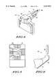
- FIG. 4is an isometric view of force sensor or gauge, in accordance with the present invention.
- FIG. 5is a camera view of the force sensor and the contact ends of probe tips, in accordance with the present invention.
- FIG. 6shows a macro view of a probe tip and shim contact scenario from FIG. 4.
- FIG. 7is a graph illustrating an example of the probe tips' spring relationship.
- An integrated probe tip parameter measuring deviceis integrated onto the chuck (substrate holder) of a probe station.
- Probe tip forcecan be measured for either a single probe tip, several probe tips, or all the probe tips on a probe card. Integrating the measurement of probe tip force into a test station yields quick-time data about the probe process.
- One advantage that this providesis to allow feedback between measured probe tip force and chuck overdrive in the Z direction.
- FIG. 1is a cross-sectional view of a probe test station ("tester") 10.
- the tester 10has a test head 12 and a prober 14. Connecting the test head 12 to a probe card 18 is a probe interface 16.
- probe tips 20are cantilever probes, Cobra needle probes, and membrane bumps, and other compliant contact technologies. Other technologies are envisioned.
- Probe tips 20electrically connect device under test (DUT) in a wafer 22 to the test head 12.
- a prober chuck 24moves a wafer 22, and the die 26 within the wafer 22 in X, Y, and Z directions in order to connect the probe tips 20 contact points on each individual die 26.
- FIG. 2is a top view of the chuck top in the tester 10 in FIG. 1.
- a semiconductor wafer 22comprised of a plurality of die sits on the chuck 24. Attached to the chuck 24 itself are three potential occasions for probe tip parameter measurement.
- a camera 32is typically used for alignment. However, it can provide a view of the probe tips and a sensor target at the same time.
- a probe tip cleaning device 34is typically used to clean probe tips 20 periodically. It operates by briefly touching the bottoms of the probe tips 20 in a sand paper fashion. This is done at every "N" number of die.
- an independent force measurement station 36can be installed that automatically measures the probe tip 20 force for one or more probe tips 20 at a time. Note that the probe parameter sensor can be integrated into any of these three locations, camera 32, probe tip cleaning device 34, and independent force measurement station 36. In the case of the probe tip cleaning device 34, the act of cleaning probe tips 20 can be integrated into measuring probe tip parameters simultaneously.
- Probe tipscan either be tested individually, or in a group. Groups may range from two up to all of the probe tips attached to a probe card. Advantages of testing a single probe tip include identifying which probe tip attached to a probe card is posing a failure. One advantage of testing all probe tips attached to a probe card simultaneously is the savings in time where the individual force is derived from dividing the total probe tip force by the number of probe tips making full contact. Likewise, an average spring constant can be found from dividing by the probe tips' compressed "Z" height.
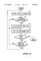
- a testis made whether the probe tip or tips are within specification, step 52. If not within specification, step 52, the probe card can be either fixed or replaced, step 54. In any case, a die on a substrate or wafer is tested with the probe card, step 56. A measurement is then made whether there are more die to test, step 58. If no more die remain to be tested, step 58, the process is complete. Otherwise, a measurement is made whether to measure probe tip parameters, step 60. Probe tip parameters can be measured for example on a per substrate or wafer basis, or on a lot basis, or after a certain number of die have been probed or tested. Indeed, it is possible to dynamically adjust the testing frequency of measuring probe tip parameters by the characteristics measured in step 50. If it is not yet time to measure probe tip parameters, step 60, the next die is tested with the probe card, step 56. Otherwise, the probe tip parameter for the probe card is measured, step 50, before entering into the inner loop.
- FIG. 4is an isometric view of force sensor or gauge 70.
- the force sensor 70is accurate to a tenth of a gram. This is sufficiently accurate for the purposes described herein. However, it is envisioned that this accuracy will improve over time.
- the force sensor 70has an arm 72, and a shim 74 attached to the arm 72 with a plate 76.
- the shim 74has a raised section 78. Shims 74 can vary in width, with the width selected determined by the number of probe tips 20 to test simultaneously. Typically, each of the shims has a width in a range of approximately 50-1,250 microns.
- the implementation of the force sensor 70 showncan be used with a camera 32. However, in the case of the integrated probe tip cleaning device 34, no arm 72 would be necessary, rather just the full tip contact pad 84. Especially in the case of a force sensor 70 for measuring all of the probe tips 20 at a single time, other equivalent configurations and designs are possible.
- a uni-directional force sensor 70 or load cellis sufficient.
- the force sensor 70is accurately mounted such that the direction of applied load is within the same axis of the sensor's measurement axis.
- the force sensor 70has a nonlinearity, hysteresis, and nonrepeatability of +/-0.02%.
- a force sensor 70 that makes use of a "4-arm strain-gage bridge" to convert a strain to a voltageallows for these values to be achieved.
- Futek Advanced Sensor Technology, Inc.(26052 Merit Circle, Suite 103, Madison Hills, Calif. 92653) is a company that is able to provide sensors within these operating specifications.
- the force sensor 70 utilizedshould also be able to operate within the temperature range of -20° C. to 90° C.
- FIG. 5is a camera view of the force sensor 70 and probe tip contacts 82 that are the contact ends of probe tips 20.
- the force sensor 70, arm 72contains the shim 74.
- At the end of the shim 74is a tip or raised surface 78.
- the shim's raised surface 78engages probe tip contact 82, when moved in a "Z" or vertical direction, moves the probe tip contact 82. Resistance to this movement is then measured by the force sensor 70.
- FIG. 6shows a macro view of a probe tip contact 82 and shim 74 contact scenario from FIG. 4.
- the shim 74has a tipped or raised surface 78. It is supported by the arm 72.
- raised surface 78has a surface that is substantially parallel to the top surface of the arm (body) 72. The elevational different between the raised surface and the top surface is in a range of approximately 50-500 microns.
- the sensor 70moves up in a vertical or "Z" direction
- the raised surface 78engages and depresses the probe tip contact 82 deflecting the probe tip 20 upward.
- the absolute relative resistance of the probe tip contact 82 to movement induced by the raised surface 78can be measured, and this measure can be used to accomplish the objectives of the measuring probe tip behavior under load.
- probe tips 20can be tested periodically, for example after each wafer, after every lot, or after "N" number of die.
- the probe height distancecan be adjusted based on the decay shown in solid line curve 94.
- actual data for a set of probe tips 20can be compared with expected values, and the lifetime of a probe card 18 determined from such.
- This datacan also be used to decrease the deformation created on the bond pads or bumps by the physical contact of the probe tips 20.
- This datacan also be tied in or integrated with electrical data such as contact resistance between the probe tips 20 and wafer metallurgy.
Landscapes
- Physics & Mathematics (AREA)
- General Physics & Mathematics (AREA)
- Engineering & Computer Science (AREA)
- General Engineering & Computer Science (AREA)
- Measuring Leads Or Probes (AREA)
- Testing Or Measuring Of Semiconductors Or The Like (AREA)
- Testing Of Individual Semiconductor Devices (AREA)
- Tests Of Electronic Circuits (AREA)
Abstract
Description
Claims (17)
Priority Applications (2)
| Application Number | Priority Date | Filing Date | Title |
|---|---|---|---|
| US08/844,577US6127831A (en) | 1997-04-21 | 1997-04-21 | Method of testing a semiconductor device by automatically measuring probe tip parameters |
| JP12680898AJP4308938B2 (en) | 1997-04-21 | 1998-04-21 | Inspection method of semiconductor elements by automatic measurement of probe tip parameters |
Applications Claiming Priority (1)
| Application Number | Priority Date | Filing Date | Title |
|---|---|---|---|
| US08/844,577US6127831A (en) | 1997-04-21 | 1997-04-21 | Method of testing a semiconductor device by automatically measuring probe tip parameters |
Publications (1)
| Publication Number | Publication Date |
|---|---|
| US6127831Atrue US6127831A (en) | 2000-10-03 |
Family
ID=25293118
Family Applications (1)
| Application Number | Title | Priority Date | Filing Date |
|---|---|---|---|
| US08/844,577Expired - LifetimeUS6127831A (en) | 1997-04-21 | 1997-04-21 | Method of testing a semiconductor device by automatically measuring probe tip parameters |
Country Status (2)
| Country | Link |
|---|---|
| US (1) | US6127831A (en) |
| JP (1) | JP4308938B2 (en) |
Cited By (62)
| Publication number | Priority date | Publication date | Assignee | Title |
|---|---|---|---|---|
| US6720789B1 (en) | 2003-02-13 | 2004-04-13 | International Business Machines Corporation | Method for wafer test and wafer test system for implementing the method |
| US6777966B1 (en)* | 1999-07-30 | 2004-08-17 | International Test Solutions, Inc. | Cleaning system, device and method |
| WO2004070399A1 (en)* | 2003-02-05 | 2004-08-19 | Systems On Silicon Manufacturing Co. Pte. Ltd. | A method for detecting and monitoring wafer probing process instability |
| WO2004070405A1 (en)* | 2003-02-05 | 2004-08-19 | Systems On Silicon Manufacturing Co. Pte. Ltd. | Probe card needle cleaning frequency optimization |
| US20050001645A1 (en)* | 1999-07-30 | 2005-01-06 | Humphrey Alan E. | Cleaning system, device and method |
| US20050040837A1 (en)* | 1995-04-14 | 2005-02-24 | Strid Eric W. | System for evaluating probing networks |
| US20050116734A1 (en)* | 2003-12-02 | 2005-06-02 | Savagaonkar Uday R. | Dynamic overdrive compensation test system and method |
| US20050258835A1 (en)* | 2002-08-27 | 2005-11-24 | Masakatsu Saijyo | Method of measuring contact resistance of probe and method of testing semiconductor device |
| US20060008226A1 (en)* | 2001-05-04 | 2006-01-12 | Cascade Microtech, Inc. | Fiber optic wafer probe |
| US20060066322A1 (en)* | 2004-09-29 | 2006-03-30 | Fitzgerald David J | Semiconductor testing |
| US7138813B2 (en) | 1999-06-30 | 2006-11-21 | Cascade Microtech, Inc. | Probe station thermal chuck with shielding for capacitive current |
| US7138810B2 (en) | 2002-11-08 | 2006-11-21 | Cascade Microtech, Inc. | Probe station with low noise characteristics |
| US7161363B2 (en) | 2002-05-23 | 2007-01-09 | Cascade Microtech, Inc. | Probe for testing a device under test |
| US7176705B2 (en) | 2004-06-07 | 2007-02-13 | Cascade Microtech, Inc. | Thermal optical chuck |
| US7187188B2 (en) | 2003-12-24 | 2007-03-06 | Cascade Microtech, Inc. | Chuck with integrated wafer support |
| US7190181B2 (en) | 1997-06-06 | 2007-03-13 | Cascade Microtech, Inc. | Probe station having multiple enclosures |
| US7221172B2 (en) | 2003-05-06 | 2007-05-22 | Cascade Microtech, Inc. | Switched suspended conductor and connection |
| US7221146B2 (en) | 2002-12-13 | 2007-05-22 | Cascade Microtech, Inc. | Guarded tub enclosure |
| US7233160B2 (en) | 2000-12-04 | 2007-06-19 | Cascade Microtech, Inc. | Wafer probe |
| US7250779B2 (en) | 2002-11-25 | 2007-07-31 | Cascade Microtech, Inc. | Probe station with low inductance path |
| US7250626B2 (en) | 2003-10-22 | 2007-07-31 | Cascade Microtech, Inc. | Probe testing structure |
| US7268533B2 (en) | 2001-08-31 | 2007-09-11 | Cascade Microtech, Inc. | Optical testing device |
| US7271603B2 (en) | 2003-05-23 | 2007-09-18 | Cascade Microtech, Inc. | Shielded probe for testing a device under test |
| US7285969B2 (en) | 2002-11-13 | 2007-10-23 | Cascade Microtech, Inc. | Probe for combined signals |
| US7330023B2 (en) | 1992-06-11 | 2008-02-12 | Cascade Microtech, Inc. | Wafer probe station having a skirting component |
| US7330041B2 (en) | 2004-06-14 | 2008-02-12 | Cascade Microtech, Inc. | Localizing a temperature of a device for testing |
| US7348787B2 (en) | 1992-06-11 | 2008-03-25 | Cascade Microtech, Inc. | Wafer probe station having environment control enclosure |
| US7352168B2 (en) | 2000-09-05 | 2008-04-01 | Cascade Microtech, Inc. | Chuck for holding a device under test |
| US7355420B2 (en) | 2001-08-21 | 2008-04-08 | Cascade Microtech, Inc. | Membrane probing system |
| US7368925B2 (en) | 2002-01-25 | 2008-05-06 | Cascade Microtech, Inc. | Probe station with two platens |
| US7368927B2 (en) | 2004-07-07 | 2008-05-06 | Cascade Microtech, Inc. | Probe head having a membrane suspended probe |
| WO2008079307A1 (en)* | 2006-12-19 | 2008-07-03 | Rudolph Technologies, Inc. | Probe card analysis system and method |
| US7403025B2 (en) | 2000-02-25 | 2008-07-22 | Cascade Microtech, Inc. | Membrane probing system |
| US7403028B2 (en) | 2006-06-12 | 2008-07-22 | Cascade Microtech, Inc. | Test structure and probe for differential signals |
| US7420381B2 (en) | 2004-09-13 | 2008-09-02 | Cascade Microtech, Inc. | Double sided probing structures |
| US7427868B2 (en) | 2003-12-24 | 2008-09-23 | Cascade Microtech, Inc. | Active wafer probe |
| US7443186B2 (en) | 2006-06-12 | 2008-10-28 | Cascade Microtech, Inc. | On-wafer test structures for differential signals |
| US7449899B2 (en) | 2005-06-08 | 2008-11-11 | Cascade Microtech, Inc. | Probe for high frequency signals |
| US7492172B2 (en) | 2003-05-23 | 2009-02-17 | Cascade Microtech, Inc. | Chuck for holding a device under test |
| US7504842B2 (en) | 1997-05-28 | 2009-03-17 | Cascade Microtech, Inc. | Probe holder for testing of a test device |
| US7533462B2 (en) | 1999-06-04 | 2009-05-19 | Cascade Microtech, Inc. | Method of constructing a membrane probe |
| US7535247B2 (en) | 2005-01-31 | 2009-05-19 | Cascade Microtech, Inc. | Interface for testing semiconductors |
| US7541821B2 (en) | 1996-08-08 | 2009-06-02 | Cascade Microtech, Inc. | Membrane probing system with local contact scrub |
| US7554322B2 (en) | 2000-09-05 | 2009-06-30 | Cascade Microtech, Inc. | Probe station |
| US7609077B2 (en) | 2006-06-09 | 2009-10-27 | Cascade Microtech, Inc. | Differential signal probe with integral balun |
| US7619419B2 (en) | 2005-06-13 | 2009-11-17 | Cascade Microtech, Inc. | Wideband active-passive differential signal probe |
| US7656172B2 (en) | 2005-01-31 | 2010-02-02 | Cascade Microtech, Inc. | System for testing semiconductors |
| US7681312B2 (en) | 1998-07-14 | 2010-03-23 | Cascade Microtech, Inc. | Membrane probing system |
| US7723999B2 (en) | 2006-06-12 | 2010-05-25 | Cascade Microtech, Inc. | Calibration structures for differential signal probing |
| US7764072B2 (en) | 2006-06-12 | 2010-07-27 | Cascade Microtech, Inc. | Differential signal probing system |
| US7876114B2 (en) | 2007-08-08 | 2011-01-25 | Cascade Microtech, Inc. | Differential waveguide probe |
| US7888957B2 (en) | 2008-10-06 | 2011-02-15 | Cascade Microtech, Inc. | Probing apparatus with impedance optimized interface |
| US20110089965A1 (en)* | 2003-03-14 | 2011-04-21 | Rudolph Technologies, Inc. | Probe card analysis system and method |
| US8319503B2 (en) | 2008-11-24 | 2012-11-27 | Cascade Microtech, Inc. | Test apparatus for measuring a characteristic of a device under test |
| US20130071958A1 (en)* | 2011-09-20 | 2013-03-21 | Renesas Electronics Corporation | Manufacturing method of semiconductor integrated circuit device |
| US8410806B2 (en) | 2008-11-21 | 2013-04-02 | Cascade Microtech, Inc. | Replaceable coupon for a probing apparatus |
| US8838408B2 (en) | 2010-11-11 | 2014-09-16 | Optimal Plus Ltd | Misalignment indication decision system and method |
| WO2015130573A1 (en)* | 2014-02-25 | 2015-09-03 | Cascade Microtech, Inc. | Systems and methods for on-wafer dynamic testing of electronic devices |
| US20160077147A1 (en)* | 2014-09-17 | 2016-03-17 | Taiwan Semiconductor Manufacturing Company, Ltd. | Integrated fan-out pillar probe system |
| US20170292832A1 (en)* | 2016-04-08 | 2017-10-12 | Infineon Technologies Ag | Wafer probing |
| US20180259555A1 (en)* | 2017-03-10 | 2018-09-13 | Win Semiconductors Corp. | Prober and method for positioning probe tip and obtaining probe and polishing sheet contact data |
| CN115469203A (en)* | 2022-09-05 | 2022-12-13 | 上海泽丰半导体科技有限公司 | Probe card stroke measuring system and method |
Families Citing this family (4)
| Publication number | Priority date | Publication date | Assignee | Title |
|---|---|---|---|---|
| JP4134940B2 (en)* | 2004-04-22 | 2008-08-20 | トヨタ自動車株式会社 | Performance board diagnostic method and diagnostic device |
| KR100647538B1 (en) | 2005-07-12 | 2006-11-23 | (주)피프러스 | Dip capped semiconductor chip test probe system |
| CN105629151A (en)* | 2015-12-16 | 2016-06-01 | 珠海市运泰利自动化设备有限公司 | Precision test probe module set |
| KR102430476B1 (en)* | 2016-05-09 | 2022-08-08 | 세메스 주식회사 | Method of managing probe card |
Citations (10)
| Publication number | Priority date | Publication date | Assignee | Title |
|---|---|---|---|---|
| US3628144A (en)* | 1969-01-15 | 1971-12-14 | Ibm | Electrical contact cleaning device |
| US4195259A (en)* | 1978-04-04 | 1980-03-25 | Texas Instruments Incorporated | Multiprobe test system and method of using same |
| US4590422A (en)* | 1981-07-30 | 1986-05-20 | Pacific Western Systems, Inc. | Automatic wafer prober having a probe scrub routine |
| US4673839A (en)* | 1986-09-08 | 1987-06-16 | Tektronix, Inc. | Piezoelectric pressure sensing apparatus for integrated circuit testing stations |
| US4918374A (en)* | 1988-10-05 | 1990-04-17 | Applied Precision, Inc. | Method and apparatus for inspecting integrated circuit probe cards |
| US5065092A (en)* | 1990-05-14 | 1991-11-12 | Triple S Engineering, Inc. | System for locating probe tips on an integrated circuit probe card and method therefor |
| US5220279A (en)* | 1991-06-12 | 1993-06-15 | Tokyo Electron Yamanashi Limited | Probe apparatus |
| US5561377A (en)* | 1995-04-14 | 1996-10-01 | Cascade Microtech, Inc. | System for evaluating probing networks |
| US5778485A (en)* | 1995-01-19 | 1998-07-14 | Tokyo Electron Limited | Probe card cleaning apparatus, probe apparatus with the cleaning apparatus, and probe card cleaning method |
| US5968282A (en)* | 1997-11-10 | 1999-10-19 | Tokyo Electron Limited | Mechanism and method for cleaning probe needles |
- 1997
- 1997-04-21USUS08/844,577patent/US6127831A/ennot_activeExpired - Lifetime
- 1998
- 1998-04-21JPJP12680898Apatent/JP4308938B2/ennot_activeExpired - Fee Related
Patent Citations (11)
| Publication number | Priority date | Publication date | Assignee | Title |
|---|---|---|---|---|
| US3628144A (en)* | 1969-01-15 | 1971-12-14 | Ibm | Electrical contact cleaning device |
| US4195259A (en)* | 1978-04-04 | 1980-03-25 | Texas Instruments Incorporated | Multiprobe test system and method of using same |
| US4590422A (en)* | 1981-07-30 | 1986-05-20 | Pacific Western Systems, Inc. | Automatic wafer prober having a probe scrub routine |
| US4673839A (en)* | 1986-09-08 | 1987-06-16 | Tektronix, Inc. | Piezoelectric pressure sensing apparatus for integrated circuit testing stations |
| US4918374A (en)* | 1988-10-05 | 1990-04-17 | Applied Precision, Inc. | Method and apparatus for inspecting integrated circuit probe cards |
| US5065092A (en)* | 1990-05-14 | 1991-11-12 | Triple S Engineering, Inc. | System for locating probe tips on an integrated circuit probe card and method therefor |
| US5220279A (en)* | 1991-06-12 | 1993-06-15 | Tokyo Electron Yamanashi Limited | Probe apparatus |
| US5778485A (en)* | 1995-01-19 | 1998-07-14 | Tokyo Electron Limited | Probe card cleaning apparatus, probe apparatus with the cleaning apparatus, and probe card cleaning method |
| US5561377A (en)* | 1995-04-14 | 1996-10-01 | Cascade Microtech, Inc. | System for evaluating probing networks |
| US5659255A (en)* | 1995-04-14 | 1997-08-19 | Cascade Microtech, Inc. | Method of evaluating signal conditions in a probe measurement network having a plurality of separate measurement channels |
| US5968282A (en)* | 1997-11-10 | 1999-10-19 | Tokyo Electron Limited | Mechanism and method for cleaning probe needles |
Cited By (130)
| Publication number | Priority date | Publication date | Assignee | Title |
|---|---|---|---|---|
| US7348787B2 (en) | 1992-06-11 | 2008-03-25 | Cascade Microtech, Inc. | Wafer probe station having environment control enclosure |
| US7589518B2 (en) | 1992-06-11 | 2009-09-15 | Cascade Microtech, Inc. | Wafer probe station having a skirting component |
| US7595632B2 (en) | 1992-06-11 | 2009-09-29 | Cascade Microtech, Inc. | Wafer probe station having environment control enclosure |
| US7492147B2 (en) | 1992-06-11 | 2009-02-17 | Cascade Microtech, Inc. | Wafer probe station having a skirting component |
| US7330023B2 (en) | 1992-06-11 | 2008-02-12 | Cascade Microtech, Inc. | Wafer probe station having a skirting component |
| US7164279B2 (en) | 1995-04-14 | 2007-01-16 | Cascade Microtech, Inc. | System for evaluating probing networks |
| US20050040837A1 (en)* | 1995-04-14 | 2005-02-24 | Strid Eric W. | System for evaluating probing networks |
| US7321233B2 (en) | 1995-04-14 | 2008-01-22 | Cascade Microtech, Inc. | System for evaluating probing networks |
| US6987398B2 (en)* | 1995-04-14 | 2006-01-17 | Cascade Microtech, Inc. | System for evaluating probing networks |
| US7893704B2 (en) | 1996-08-08 | 2011-02-22 | Cascade Microtech, Inc. | Membrane probing structure with laterally scrubbing contacts |
| US7541821B2 (en) | 1996-08-08 | 2009-06-02 | Cascade Microtech, Inc. | Membrane probing system with local contact scrub |
| US7504842B2 (en) | 1997-05-28 | 2009-03-17 | Cascade Microtech, Inc. | Probe holder for testing of a test device |
| US7436170B2 (en) | 1997-06-06 | 2008-10-14 | Cascade Microtech, Inc. | Probe station having multiple enclosures |
| US7626379B2 (en) | 1997-06-06 | 2009-12-01 | Cascade Microtech, Inc. | Probe station having multiple enclosures |
| US7190181B2 (en) | 1997-06-06 | 2007-03-13 | Cascade Microtech, Inc. | Probe station having multiple enclosures |
| US8451017B2 (en) | 1998-07-14 | 2013-05-28 | Cascade Microtech, Inc. | Membrane probing method using improved contact |
| US7761986B2 (en) | 1998-07-14 | 2010-07-27 | Cascade Microtech, Inc. | Membrane probing method using improved contact |
| US7681312B2 (en) | 1998-07-14 | 2010-03-23 | Cascade Microtech, Inc. | Membrane probing system |
| US7533462B2 (en) | 1999-06-04 | 2009-05-19 | Cascade Microtech, Inc. | Method of constructing a membrane probe |
| US7138813B2 (en) | 1999-06-30 | 2006-11-21 | Cascade Microtech, Inc. | Probe station thermal chuck with shielding for capacitive current |
| US7292057B2 (en) | 1999-06-30 | 2007-11-06 | Cascade Microtech, Inc. | Probe station thermal chuck with shielding for capacitive current |
| US7616017B2 (en) | 1999-06-30 | 2009-11-10 | Cascade Microtech, Inc. | Probe station thermal chuck with shielding for capacitive current |
| US20050001645A1 (en)* | 1999-07-30 | 2005-01-06 | Humphrey Alan E. | Cleaning system, device and method |
| US7202683B2 (en)* | 1999-07-30 | 2007-04-10 | International Test Solutions | Cleaning system, device and method |
| US6777966B1 (en)* | 1999-07-30 | 2004-08-17 | International Test Solutions, Inc. | Cleaning system, device and method |
| US20060001438A1 (en)* | 1999-07-30 | 2006-01-05 | International Test Solutions, Inc. | Cleaning system, device and method |
| US7403025B2 (en) | 2000-02-25 | 2008-07-22 | Cascade Microtech, Inc. | Membrane probing system |
| US7554322B2 (en) | 2000-09-05 | 2009-06-30 | Cascade Microtech, Inc. | Probe station |
| US7352168B2 (en) | 2000-09-05 | 2008-04-01 | Cascade Microtech, Inc. | Chuck for holding a device under test |
| US7518358B2 (en) | 2000-09-05 | 2009-04-14 | Cascade Microtech, Inc. | Chuck for holding a device under test |
| US7423419B2 (en) | 2000-09-05 | 2008-09-09 | Cascade Microtech, Inc. | Chuck for holding a device under test |
| US7969173B2 (en) | 2000-09-05 | 2011-06-28 | Cascade Microtech, Inc. | Chuck for holding a device under test |
| US7514915B2 (en) | 2000-09-05 | 2009-04-07 | Cascade Microtech, Inc. | Chuck for holding a device under test |
| US7688062B2 (en) | 2000-09-05 | 2010-03-30 | Cascade Microtech, Inc. | Probe station |
| US7501810B2 (en) | 2000-09-05 | 2009-03-10 | Cascade Microtech, Inc. | Chuck for holding a device under test |
| US7456646B2 (en) | 2000-12-04 | 2008-11-25 | Cascade Microtech, Inc. | Wafer probe |
| US7233160B2 (en) | 2000-12-04 | 2007-06-19 | Cascade Microtech, Inc. | Wafer probe |
| US7495461B2 (en) | 2000-12-04 | 2009-02-24 | Cascade Microtech, Inc. | Wafer probe |
| US7688097B2 (en) | 2000-12-04 | 2010-03-30 | Cascade Microtech, Inc. | Wafer probe |
| US7761983B2 (en) | 2000-12-04 | 2010-07-27 | Cascade Microtech, Inc. | Method of assembling a wafer probe |
| US7298536B2 (en) | 2001-05-04 | 2007-11-20 | Cascade Microtech, Inc. | Fiber optic wafer probe |
| US20060008226A1 (en)* | 2001-05-04 | 2006-01-12 | Cascade Microtech, Inc. | Fiber optic wafer probe |
| US7355420B2 (en) | 2001-08-21 | 2008-04-08 | Cascade Microtech, Inc. | Membrane probing system |
| US7492175B2 (en) | 2001-08-21 | 2009-02-17 | Cascade Microtech, Inc. | Membrane probing system |
| US7268533B2 (en) | 2001-08-31 | 2007-09-11 | Cascade Microtech, Inc. | Optical testing device |
| US7368925B2 (en) | 2002-01-25 | 2008-05-06 | Cascade Microtech, Inc. | Probe station with two platens |
| US7304488B2 (en) | 2002-05-23 | 2007-12-04 | Cascade Microtech, Inc. | Shielded probe for high-frequency testing of a device under test |
| US7161363B2 (en) | 2002-05-23 | 2007-01-09 | Cascade Microtech, Inc. | Probe for testing a device under test |
| US7489149B2 (en) | 2002-05-23 | 2009-02-10 | Cascade Microtech, Inc. | Shielded probe for testing a device under test |
| US7482823B2 (en) | 2002-05-23 | 2009-01-27 | Cascade Microtech, Inc. | Shielded probe for testing a device under test |
| US7518387B2 (en) | 2002-05-23 | 2009-04-14 | Cascade Microtech, Inc. | Shielded probe for testing a device under test |
| US7436194B2 (en) | 2002-05-23 | 2008-10-14 | Cascade Microtech, Inc. | Shielded probe with low contact resistance for testing a device under test |
| US20050258835A1 (en)* | 2002-08-27 | 2005-11-24 | Masakatsu Saijyo | Method of measuring contact resistance of probe and method of testing semiconductor device |
| US7295025B2 (en) | 2002-11-08 | 2007-11-13 | Cascade Microtech, Inc. | Probe station with low noise characteristics |
| US7138810B2 (en) | 2002-11-08 | 2006-11-21 | Cascade Microtech, Inc. | Probe station with low noise characteristics |
| US7550984B2 (en) | 2002-11-08 | 2009-06-23 | Cascade Microtech, Inc. | Probe station with low noise characteristics |
| US7285969B2 (en) | 2002-11-13 | 2007-10-23 | Cascade Microtech, Inc. | Probe for combined signals |
| US7453276B2 (en) | 2002-11-13 | 2008-11-18 | Cascade Microtech, Inc. | Probe for combined signals |
| US7417446B2 (en) | 2002-11-13 | 2008-08-26 | Cascade Microtech, Inc. | Probe for combined signals |
| US7250779B2 (en) | 2002-11-25 | 2007-07-31 | Cascade Microtech, Inc. | Probe station with low inductance path |
| US7498828B2 (en) | 2002-11-25 | 2009-03-03 | Cascade Microtech, Inc. | Probe station with low inductance path |
| US7221146B2 (en) | 2002-12-13 | 2007-05-22 | Cascade Microtech, Inc. | Guarded tub enclosure |
| US7639003B2 (en) | 2002-12-13 | 2009-12-29 | Cascade Microtech, Inc. | Guarded tub enclosure |
| WO2004070399A1 (en)* | 2003-02-05 | 2004-08-19 | Systems On Silicon Manufacturing Co. Pte. Ltd. | A method for detecting and monitoring wafer probing process instability |
| US7230439B2 (en)* | 2003-02-05 | 2007-06-12 | Systems On Silicon Manufacturing Co. Pte. Ltd. | Method for detecting and monitoring wafer probing process instability |
| US20060149505A1 (en)* | 2003-02-05 | 2006-07-06 | Systems On Silicon Manufacturing Co. Pte Ltd. | Method for detecting and monitoring wafer probing process instability |
| WO2004070405A1 (en)* | 2003-02-05 | 2004-08-19 | Systems On Silicon Manufacturing Co. Pte. Ltd. | Probe card needle cleaning frequency optimization |
| US6720789B1 (en) | 2003-02-13 | 2004-04-13 | International Business Machines Corporation | Method for wafer test and wafer test system for implementing the method |
| US20140021970A1 (en)* | 2003-03-14 | 2014-01-23 | Rudolph Technologies, Inc. | Probe card analysis system and method |
| US8466703B2 (en) | 2003-03-14 | 2013-06-18 | Rudolph Technologies, Inc. | Probe card analysis system and method |
| US9638782B2 (en)* | 2003-03-14 | 2017-05-02 | Rudolph Technologies, Inc. | Probe card analysis system and method |
| US20110089965A1 (en)* | 2003-03-14 | 2011-04-21 | Rudolph Technologies, Inc. | Probe card analysis system and method |
| US7221172B2 (en) | 2003-05-06 | 2007-05-22 | Cascade Microtech, Inc. | Switched suspended conductor and connection |
| US7468609B2 (en) | 2003-05-06 | 2008-12-23 | Cascade Microtech, Inc. | Switched suspended conductor and connection |
| US7498829B2 (en) | 2003-05-23 | 2009-03-03 | Cascade Microtech, Inc. | Shielded probe for testing a device under test |
| US7898273B2 (en) | 2003-05-23 | 2011-03-01 | Cascade Microtech, Inc. | Probe for testing a device under test |
| US7271603B2 (en) | 2003-05-23 | 2007-09-18 | Cascade Microtech, Inc. | Shielded probe for testing a device under test |
| US7876115B2 (en) | 2003-05-23 | 2011-01-25 | Cascade Microtech, Inc. | Chuck for holding a device under test |
| US7501842B2 (en) | 2003-05-23 | 2009-03-10 | Cascade Microtech, Inc. | Shielded probe for testing a device under test |
| US7492172B2 (en) | 2003-05-23 | 2009-02-17 | Cascade Microtech, Inc. | Chuck for holding a device under test |
| US7250626B2 (en) | 2003-10-22 | 2007-07-31 | Cascade Microtech, Inc. | Probe testing structure |
| US8069491B2 (en) | 2003-10-22 | 2011-11-29 | Cascade Microtech, Inc. | Probe testing structure |
| US20050116734A1 (en)* | 2003-12-02 | 2005-06-02 | Savagaonkar Uday R. | Dynamic overdrive compensation test system and method |
| US7129733B2 (en)* | 2003-12-02 | 2006-10-31 | Intel Corporation | Dynamic overdrive compensation test system and method |
| US7688091B2 (en) | 2003-12-24 | 2010-03-30 | Cascade Microtech, Inc. | Chuck with integrated wafer support |
| US7427868B2 (en) | 2003-12-24 | 2008-09-23 | Cascade Microtech, Inc. | Active wafer probe |
| US7362115B2 (en) | 2003-12-24 | 2008-04-22 | Cascade Microtech, Inc. | Chuck with integrated wafer support |
| US7759953B2 (en) | 2003-12-24 | 2010-07-20 | Cascade Microtech, Inc. | Active wafer probe |
| US7187188B2 (en) | 2003-12-24 | 2007-03-06 | Cascade Microtech, Inc. | Chuck with integrated wafer support |
| US7504823B2 (en) | 2004-06-07 | 2009-03-17 | Cascade Microtech, Inc. | Thermal optical chuck |
| US7176705B2 (en) | 2004-06-07 | 2007-02-13 | Cascade Microtech, Inc. | Thermal optical chuck |
| US7330041B2 (en) | 2004-06-14 | 2008-02-12 | Cascade Microtech, Inc. | Localizing a temperature of a device for testing |
| US7368927B2 (en) | 2004-07-07 | 2008-05-06 | Cascade Microtech, Inc. | Probe head having a membrane suspended probe |
| US7514944B2 (en) | 2004-07-07 | 2009-04-07 | Cascade Microtech, Inc. | Probe head having a membrane suspended probe |
| US7420381B2 (en) | 2004-09-13 | 2008-09-02 | Cascade Microtech, Inc. | Double sided probing structures |
| US8013623B2 (en) | 2004-09-13 | 2011-09-06 | Cascade Microtech, Inc. | Double sided probing structures |
| US20060066322A1 (en)* | 2004-09-29 | 2006-03-30 | Fitzgerald David J | Semiconductor testing |
| US7084648B2 (en) | 2004-09-29 | 2006-08-01 | Agere Systems Inc. | Semiconductor testing |
| US7656172B2 (en) | 2005-01-31 | 2010-02-02 | Cascade Microtech, Inc. | System for testing semiconductors |
| US7940069B2 (en) | 2005-01-31 | 2011-05-10 | Cascade Microtech, Inc. | System for testing semiconductors |
| US7898281B2 (en) | 2005-01-31 | 2011-03-01 | Cascade Mircotech, Inc. | Interface for testing semiconductors |
| US7535247B2 (en) | 2005-01-31 | 2009-05-19 | Cascade Microtech, Inc. | Interface for testing semiconductors |
| US7449899B2 (en) | 2005-06-08 | 2008-11-11 | Cascade Microtech, Inc. | Probe for high frequency signals |
| US7619419B2 (en) | 2005-06-13 | 2009-11-17 | Cascade Microtech, Inc. | Wideband active-passive differential signal probe |
| US7609077B2 (en) | 2006-06-09 | 2009-10-27 | Cascade Microtech, Inc. | Differential signal probe with integral balun |
| US7723999B2 (en) | 2006-06-12 | 2010-05-25 | Cascade Microtech, Inc. | Calibration structures for differential signal probing |
| US7443186B2 (en) | 2006-06-12 | 2008-10-28 | Cascade Microtech, Inc. | On-wafer test structures for differential signals |
| US7764072B2 (en) | 2006-06-12 | 2010-07-27 | Cascade Microtech, Inc. | Differential signal probing system |
| US7403028B2 (en) | 2006-06-12 | 2008-07-22 | Cascade Microtech, Inc. | Test structure and probe for differential signals |
| US7750652B2 (en) | 2006-06-12 | 2010-07-06 | Cascade Microtech, Inc. | Test structure and probe for differential signals |
| US7782071B2 (en) | 2006-12-19 | 2010-08-24 | Rudolph Technologies, Inc. | Probe card analysis system and method |
| WO2008079307A1 (en)* | 2006-12-19 | 2008-07-03 | Rudolph Technologies, Inc. | Probe card analysis system and method |
| US7876114B2 (en) | 2007-08-08 | 2011-01-25 | Cascade Microtech, Inc. | Differential waveguide probe |
| US7888957B2 (en) | 2008-10-06 | 2011-02-15 | Cascade Microtech, Inc. | Probing apparatus with impedance optimized interface |
| US8410806B2 (en) | 2008-11-21 | 2013-04-02 | Cascade Microtech, Inc. | Replaceable coupon for a probing apparatus |
| US10267848B2 (en) | 2008-11-21 | 2019-04-23 | Formfactor Beaverton, Inc. | Method of electrically contacting a bond pad of a device under test with a probe |
| US9429638B2 (en) | 2008-11-21 | 2016-08-30 | Cascade Microtech, Inc. | Method of replacing an existing contact of a wafer probing assembly |
| US8319503B2 (en) | 2008-11-24 | 2012-11-27 | Cascade Microtech, Inc. | Test apparatus for measuring a characteristic of a device under test |
| US8838408B2 (en) | 2010-11-11 | 2014-09-16 | Optimal Plus Ltd | Misalignment indication decision system and method |
| US8633038B2 (en)* | 2011-09-20 | 2014-01-21 | Renesas Electronics Corporation | Manufacturing method of semiconductor integrated circuit device |
| US20130071958A1 (en)* | 2011-09-20 | 2013-03-21 | Renesas Electronics Corporation | Manufacturing method of semiconductor integrated circuit device |
| WO2015130573A1 (en)* | 2014-02-25 | 2015-09-03 | Cascade Microtech, Inc. | Systems and methods for on-wafer dynamic testing of electronic devices |
| US10281518B2 (en) | 2014-02-25 | 2019-05-07 | Formfactor Beaverton, Inc. | Systems and methods for on-wafer dynamic testing of electronic devices |
| US9915699B2 (en)* | 2014-09-17 | 2018-03-13 | Taiwan Semiconductor Manufacturing Company, Ltd. | Integrated fan-out pillar probe system |
| US20160077147A1 (en)* | 2014-09-17 | 2016-03-17 | Taiwan Semiconductor Manufacturing Company, Ltd. | Integrated fan-out pillar probe system |
| US20170292832A1 (en)* | 2016-04-08 | 2017-10-12 | Infineon Technologies Ag | Wafer probing |
| US10598480B2 (en)* | 2016-04-08 | 2020-03-24 | Infineon Technologies Ag | Wafer probing |
| US20180259555A1 (en)* | 2017-03-10 | 2018-09-13 | Win Semiconductors Corp. | Prober and method for positioning probe tip and obtaining probe and polishing sheet contact data |
| CN115469203A (en)* | 2022-09-05 | 2022-12-13 | 上海泽丰半导体科技有限公司 | Probe card stroke measuring system and method |
| CN115469203B (en)* | 2022-09-05 | 2023-09-19 | 上海泽丰半导体科技有限公司 | Probe card travel measurement system and method |
Also Published As
| Publication number | Publication date |
|---|---|
| JP4308938B2 (en) | 2009-08-05 |
| JPH10303260A (en) | 1998-11-13 |
Similar Documents
| Publication | Publication Date | Title |
|---|---|---|
| US6127831A (en) | Method of testing a semiconductor device by automatically measuring probe tip parameters | |
| US6600334B1 (en) | Force applying probe card and test system for semiconductor wafers | |
| US20070176615A1 (en) | Active probe contact array management | |
| US5266895A (en) | Probe with contact portion including Au and Cu alloy | |
| JP2006329836A (en) | Contact terminal for measurement, measuring device, probe card set, wafer prober device, and testing device | |
| KR20040028645A (en) | Device for measuring characteristics of probe cards and probing method | |
| US20250093412A1 (en) | Probe structure for micro device inspection | |
| CN114994511B (en) | Bonding tester, bonding testing method and bonding testing device | |
| US7710133B2 (en) | Testing method for semiconductor device having ball-shaped external electrode | |
| US6298312B1 (en) | Method of determining the tip angle of a probe card needle | |
| JP4207690B2 (en) | Prober apparatus, probe height adjusting method, and semiconductor device manufacturing method | |
| EP4357793B1 (en) | Tilt calibration for probe systems | |
| US6720789B1 (en) | Method for wafer test and wafer test system for implementing the method | |
| KR101399542B1 (en) | Probe card | |
| JP3828299B2 (en) | Z-axis height setting apparatus and method in wafer test system | |
| JPH08330368A (en) | Semiconductor circuit device group and probe test method thereof | |
| CN113341360A (en) | Radio frequency calibration device for chip test and calibration method thereof | |
| JPH06140479A (en) | Device for testing semiconductor integrated circuit | |
| CN220982920U (en) | Integrated circuit thrust detection device | |
| JP2000111574A (en) | Probe card | |
| SE2251043A1 (en) | Microstructure inspection device and system and use of the same | |
| CN120044281A (en) | MEMS probe, probe station and test method of probe station | |
| KR200221077Y1 (en) | Conductive polymer probe card | |
| CN118962560A (en) | A terahertz frequency band probe measurement error perception feedback compensation structure and probe test calibration method | |
| Liu et al. | EXPERIMENTAL AIDED PERFORMANCE EVALUATION METHODS FOR WAFER PROBE TEST. |
Legal Events
| Date | Code | Title | Description |
|---|---|---|---|
| AS | Assignment | Owner name:MOTOROLA, INC., ILLINOIS Free format text:ASSIGNMENT OF ASSIGNORS INTEREST;ASSIGNORS:KHOURY, THEODORE ANDREW;GOODE, RAUN L.;BUSTOS, LARRY J.;REEL/FRAME:008637/0692 Effective date:19970417 | |
| STCF | Information on status: patent grant | Free format text:PATENTED CASE | |
| FPAY | Fee payment | Year of fee payment:4 | |
| AS | Assignment | Owner name:FREESCALE SEMICONDUCTOR, INC., TEXAS Free format text:ASSIGNMENT OF ASSIGNORS INTEREST;ASSIGNOR:MOTOROLA, INC.;REEL/FRAME:015698/0657 Effective date:20040404 Owner name:FREESCALE SEMICONDUCTOR, INC.,TEXAS Free format text:ASSIGNMENT OF ASSIGNORS INTEREST;ASSIGNOR:MOTOROLA, INC.;REEL/FRAME:015698/0657 Effective date:20040404 | |
| AS | Assignment | Owner name:CITIBANK, N.A. AS COLLATERAL AGENT, NEW YORK Free format text:SECURITY AGREEMENT;ASSIGNORS:FREESCALE SEMICONDUCTOR, INC.;FREESCALE ACQUISITION CORPORATION;FREESCALE ACQUISITION HOLDINGS CORP.;AND OTHERS;REEL/FRAME:018855/0129 Effective date:20061201 Owner name:CITIBANK, N.A. AS COLLATERAL AGENT,NEW YORK Free format text:SECURITY AGREEMENT;ASSIGNORS:FREESCALE SEMICONDUCTOR, INC.;FREESCALE ACQUISITION CORPORATION;FREESCALE ACQUISITION HOLDINGS CORP.;AND OTHERS;REEL/FRAME:018855/0129 Effective date:20061201 | |
| FPAY | Fee payment | Year of fee payment:8 | |
| AS | Assignment | Owner name:CITIBANK, N.A., AS COLLATERAL AGENT,NEW YORK Free format text:SECURITY AGREEMENT;ASSIGNOR:FREESCALE SEMICONDUCTOR, INC.;REEL/FRAME:024397/0001 Effective date:20100413 Owner name:CITIBANK, N.A., AS COLLATERAL AGENT, NEW YORK Free format text:SECURITY AGREEMENT;ASSIGNOR:FREESCALE SEMICONDUCTOR, INC.;REEL/FRAME:024397/0001 Effective date:20100413 | |
| FPAY | Fee payment | Year of fee payment:12 | |
| AS | Assignment | Owner name:CITIBANK, N.A., AS NOTES COLLATERAL AGENT, NEW YORK Free format text:SECURITY AGREEMENT;ASSIGNOR:FREESCALE SEMICONDUCTOR, INC.;REEL/FRAME:030633/0424 Effective date:20130521 Owner name:CITIBANK, N.A., AS NOTES COLLATERAL AGENT, NEW YOR Free format text:SECURITY AGREEMENT;ASSIGNOR:FREESCALE SEMICONDUCTOR, INC.;REEL/FRAME:030633/0424 Effective date:20130521 | |
| AS | Assignment | Owner name:CITIBANK, N.A., AS NOTES COLLATERAL AGENT, NEW YORK Free format text:SECURITY AGREEMENT;ASSIGNOR:FREESCALE SEMICONDUCTOR, INC.;REEL/FRAME:031591/0266 Effective date:20131101 Owner name:CITIBANK, N.A., AS NOTES COLLATERAL AGENT, NEW YOR Free format text:SECURITY AGREEMENT;ASSIGNOR:FREESCALE SEMICONDUCTOR, INC.;REEL/FRAME:031591/0266 Effective date:20131101 | |
| AS | Assignment | Owner name:FREESCALE SEMICONDUCTOR, INC., TEXAS Free format text:PATENT RELEASE;ASSIGNOR:CITIBANK, N.A., AS COLLATERAL AGENT;REEL/FRAME:037356/0553 Effective date:20151207 Owner name:FREESCALE SEMICONDUCTOR, INC., TEXAS Free format text:PATENT RELEASE;ASSIGNOR:CITIBANK, N.A., AS COLLATERAL AGENT;REEL/FRAME:037354/0225 Effective date:20151207 Owner name:FREESCALE SEMICONDUCTOR, INC., TEXAS Free format text:PATENT RELEASE;ASSIGNOR:CITIBANK, N.A., AS COLLATERAL AGENT;REEL/FRAME:037356/0143 Effective date:20151207 | |
| AS | Assignment | Owner name:MORGAN STANLEY SENIOR FUNDING, INC., MARYLAND Free format text:ASSIGNMENT AND ASSUMPTION OF SECURITY INTEREST IN PATENTS;ASSIGNOR:CITIBANK, N.A.;REEL/FRAME:037486/0517 Effective date:20151207 | |
| AS | Assignment | Owner name:MORGAN STANLEY SENIOR FUNDING, INC., MARYLAND Free format text:ASSIGNMENT AND ASSUMPTION OF SECURITY INTEREST IN PATENTS;ASSIGNOR:CITIBANK, N.A.;REEL/FRAME:037518/0292 Effective date:20151207 | |
| AS | Assignment | Owner name:NORTH STAR INNOVATIONS INC., CALIFORNIA Free format text:ASSIGNMENT OF ASSIGNORS INTEREST;ASSIGNOR:FREESCALE SEMICONDUCTOR, INC.;REEL/FRAME:037694/0264 Effective date:20151002 | |
| AS | Assignment | Owner name:NXP, B.V., F/K/A FREESCALE SEMICONDUCTOR, INC., NETHERLANDS Free format text:RELEASE BY SECURED PARTY;ASSIGNOR:MORGAN STANLEY SENIOR FUNDING, INC.;REEL/FRAME:040925/0001 Effective date:20160912 Owner name:NXP, B.V., F/K/A FREESCALE SEMICONDUCTOR, INC., NE Free format text:RELEASE BY SECURED PARTY;ASSIGNOR:MORGAN STANLEY SENIOR FUNDING, INC.;REEL/FRAME:040925/0001 Effective date:20160912 | |
| AS | Assignment | Owner name:NXP B.V., NETHERLANDS Free format text:RELEASE BY SECURED PARTY;ASSIGNOR:MORGAN STANLEY SENIOR FUNDING, INC.;REEL/FRAME:040928/0001 Effective date:20160622 | |
| AS | Assignment | Owner name:MORGAN STANLEY SENIOR FUNDING, INC., MARYLAND Free format text:CORRECTIVE ASSIGNMENT TO CORRECT THE REMOVE PATENTS 8108266 AND 8062324 AND REPLACE THEM WITH 6108266 AND 8060324 PREVIOUSLY RECORDED ON REEL 037518 FRAME 0292. ASSIGNOR(S) HEREBY CONFIRMS THE ASSIGNMENT AND ASSUMPTION OF SECURITY INTEREST IN PATENTS;ASSIGNOR:CITIBANK, N.A.;REEL/FRAME:041703/0536 Effective date:20151207 | |
| AS | Assignment | Owner name:SHENZHEN XINGUODU TECHNOLOGY CO., LTD., CHINA Free format text:CORRECTIVE ASSIGNMENT TO CORRECT THE TO CORRECT THE APPLICATION NO. FROM 13,883,290 TO 13,833,290 PREVIOUSLY RECORDED ON REEL 041703 FRAME 0536. ASSIGNOR(S) HEREBY CONFIRMS THE THE ASSIGNMENT AND ASSUMPTION OF SECURITYINTEREST IN PATENTS.;ASSIGNOR:MORGAN STANLEY SENIOR FUNDING, INC.;REEL/FRAME:048734/0001 Effective date:20190217 | |
| AS | Assignment | Owner name:MORGAN STANLEY SENIOR FUNDING, INC., MARYLAND Free format text:CORRECTIVE ASSIGNMENT TO CORRECT THE REMOVE APPLICATION11759915 AND REPLACE IT WITH APPLICATION 11759935 PREVIOUSLY RECORDED ON REEL 037486 FRAME 0517. ASSIGNOR(S) HEREBY CONFIRMS THE ASSIGNMENT AND ASSUMPTION OF SECURITYINTEREST IN PATENTS;ASSIGNOR:CITIBANK, N.A.;REEL/FRAME:053547/0421 Effective date:20151207 | |
| AS | Assignment | Owner name:NXP B.V., NETHERLANDS Free format text:CORRECTIVE ASSIGNMENT TO CORRECT THE REMOVEAPPLICATION 11759915 AND REPLACE IT WITH APPLICATION11759935 PREVIOUSLY RECORDED ON REEL 040928 FRAME 0001. ASSIGNOR(S) HEREBY CONFIRMS THE RELEASE OF SECURITYINTEREST;ASSIGNOR:MORGAN STANLEY SENIOR FUNDING, INC.;REEL/FRAME:052915/0001 Effective date:20160622 | |
| AS | Assignment | Owner name:NXP, B.V. F/K/A FREESCALE SEMICONDUCTOR, INC., NETHERLANDS Free format text:CORRECTIVE ASSIGNMENT TO CORRECT THE REMOVEAPPLICATION 11759915 AND REPLACE IT WITH APPLICATION11759935 PREVIOUSLY RECORDED ON REEL 040925 FRAME 0001. ASSIGNOR(S) HEREBY CONFIRMS THE RELEASE OF SECURITYINTEREST;ASSIGNOR:MORGAN STANLEY SENIOR FUNDING, INC.;REEL/FRAME:052917/0001 Effective date:20160912 |