US6127773A - Amorphic diamond film flat field emission cathode - Google Patents
Amorphic diamond film flat field emission cathodeDownload PDFInfo
- Publication number
- US6127773A US6127773AUS08/868,644US86864497AUS6127773AUS 6127773 AUS6127773 AUS 6127773AUS 86864497 AUS86864497 AUS 86864497AUS 6127773 AUS6127773 AUS 6127773A
- Authority
- US
- United States
- Prior art keywords
- cathode
- emission
- recited
- micro
- sites
- Prior art date
- Legal status (The legal status is an assumption and is not a legal conclusion. Google has not performed a legal analysis and makes no representation as to the accuracy of the status listed.)
- Expired - Fee Related
Links
- 229910003460diamondInorganic materials0.000titleclaimsabstractdescription51
- 239000010432diamondSubstances0.000titleclaimsabstractdescription51
- 239000004020conductorSubstances0.000claimsabstractdescription11
- 239000000758substrateSubstances0.000claimsdescription22
- 230000007547defectEffects0.000claimsdescription10
- 230000005684electric fieldEffects0.000claimsdescription6
- 239000000463materialSubstances0.000abstractdescription29
- 239000010408filmSubstances0.000description23
- 230000008901benefitEffects0.000description18
- 238000000034methodMethods0.000description15
- 238000004519manufacturing processMethods0.000description11
- OKTJSMMVPCPJKN-UHFFFAOYSA-NCarbonChemical compound[C]OKTJSMMVPCPJKN-UHFFFAOYSA-N0.000description10
- 229910052799carbonInorganic materials0.000description10
- 239000013078crystalSubstances0.000description10
- 238000000576coating methodMethods0.000description9
- 238000000151depositionMethods0.000description9
- 239000011248coating agentSubstances0.000description8
- 230000008569processEffects0.000description7
- OAICVXFJPJFONN-UHFFFAOYSA-NPhosphorusChemical compound[P]OAICVXFJPJFONN-UHFFFAOYSA-N0.000description6
- 230000008021depositionEffects0.000description6
- 239000002019doping agentSubstances0.000description6
- 239000011521glassSubstances0.000description6
- 125000004429atomChemical group0.000description5
- 239000004065semiconductorSubstances0.000description5
- 230000008859changeEffects0.000description4
- 238000000605extractionMethods0.000description4
- 239000011159matrix materialSubstances0.000description4
- 229910052751metalInorganic materials0.000description4
- 239000002184metalSubstances0.000description4
- 239000010409thin filmSubstances0.000description4
- 239000003463adsorbentSubstances0.000description3
- 238000001704evaporationMethods0.000description3
- 230000008020evaporationEffects0.000description3
- 238000005036potential barrierMethods0.000description3
- 239000000126substanceSubstances0.000description3
- 230000000007visual effectEffects0.000description3
- 239000002131composite materialSubstances0.000description2
- 230000001419dependent effectEffects0.000description2
- 230000005686electrostatic fieldEffects0.000description2
- 230000007613environmental effectEffects0.000description2
- 238000010438heat treatmentMethods0.000description2
- 239000012535impuritySubstances0.000description2
- 239000002245particleSubstances0.000description2
- 241000219122CucurbitaSpecies0.000description1
- 235000009804Cucurbita pepo subsp pepoNutrition0.000description1
- 238000004378air conditioningMethods0.000description1
- 229910052783alkali metalInorganic materials0.000description1
- 150000001340alkali metalsChemical class0.000description1
- 230000004075alterationEffects0.000description1
- 238000003491arrayMethods0.000description1
- 239000002585baseSubstances0.000description1
- 125000004432carbon atomChemical groupC*0.000description1
- 238000005229chemical vapour depositionMethods0.000description1
- 150000001875compoundsChemical class0.000description1
- 230000005493condensed matterEffects0.000description1
- 238000010276constructionMethods0.000description1
- 230000000694effectsEffects0.000description1
- 238000001493electron microscopyMethods0.000description1
- 230000005284excitationEffects0.000description1
- 229910002804graphiteInorganic materials0.000description1
- 239000010439graphiteSubstances0.000description1
- 239000002784hot electronSubstances0.000description1
- 238000005286illuminationMethods0.000description1
- 238000003384imaging methodMethods0.000description1
- AMGQUBHHOARCQH-UHFFFAOYSA-Nindium;oxotinChemical compound[In].[Sn]=OAMGQUBHHOARCQH-UHFFFAOYSA-N0.000description1
- 238000007737ion beam depositionMethods0.000description1
- 238000002955isolationMethods0.000description1
- 230000007246mechanismEffects0.000description1
- 238000004377microelectronicMethods0.000description1
- 238000002156mixingMethods0.000description1
- 229910021421monocrystalline siliconInorganic materials0.000description1
- 238000002360preparation methodMethods0.000description1
- 239000011347resinSubstances0.000description1
- 229920005989resinPolymers0.000description1
- 230000002441reversible effectEffects0.000description1
- 238000000926separation methodMethods0.000description1
- 125000006850spacer groupChemical group0.000description1
- 238000004544sputter depositionMethods0.000description1
- 238000006467substitution reactionMethods0.000description1
Images
Classifications
- H—ELECTRICITY
- H01—ELECTRIC ELEMENTS
- H01J—ELECTRIC DISCHARGE TUBES OR DISCHARGE LAMPS
- H01J61/00—Gas-discharge or vapour-discharge lamps
- H01J61/02—Details
- H01J61/04—Electrodes; Screens; Shields
- H01J61/06—Main electrodes
- H01J61/067—Main electrodes for low-pressure discharge lamps
- H01J61/0675—Main electrodes for low-pressure discharge lamps characterised by the material of the electrode
- H01J61/0677—Main electrodes for low-pressure discharge lamps characterised by the material of the electrode characterised by the electron emissive material
- H—ELECTRICITY
- H01—ELECTRIC ELEMENTS
- H01J—ELECTRIC DISCHARGE TUBES OR DISCHARGE LAMPS
- H01J1/00—Details of electrodes, of magnetic control means, of screens, or of the mounting or spacing thereof, common to two or more basic types of discharge tubes or lamps
- H01J1/02—Main electrodes
- H01J1/30—Cold cathodes, e.g. field-emissive cathode
- H01J1/304—Field-emissive cathodes
- H—ELECTRICITY
- H01—ELECTRIC ELEMENTS
- H01J—ELECTRIC DISCHARGE TUBES OR DISCHARGE LAMPS
- H01J63/00—Cathode-ray or electron-stream lamps
- H01J63/06—Lamps with luminescent screen excited by the ray or stream
- H—ELECTRICITY
- H01—ELECTRIC ELEMENTS
- H01J—ELECTRIC DISCHARGE TUBES OR DISCHARGE LAMPS
- H01J2201/00—Electrodes common to discharge tubes
- H01J2201/30—Cold cathodes
- H01J2201/304—Field emission cathodes
- H01J2201/30446—Field emission cathodes characterised by the emitter material
- H01J2201/30453—Carbon types
- H01J2201/30457—Diamond
- H—ELECTRICITY
- H01—ELECTRIC ELEMENTS
- H01J—ELECTRIC DISCHARGE TUBES OR DISCHARGE LAMPS
- H01J2329/00—Electron emission display panels, e.g. field emission display panels
Definitions
- This inventionrelates, in general, to flat field emission cathodes and, more particularly, to such cathodes which employ an amorphic diamond film having a plurality of emission sites situated on a flat emission surface.
- Field emissionis a phenomenon which occurs when an electric field proximate the surface of an emission material marrows a width of a potential barrier existing at the surface of the emission material. This allows a quantum tunnelling effect to occur, whereby electrons cross through the potential barrier and are emitted from the material. This is as opposed to thermionic emission, whereby thermal energy within an emission material is sufficient to eject electrons from the material.
- Thermionic emissionis a classical phenomenon
- filed emissionis a quantum mechanical phenomenon.
- the field strength required to initiate field emission of electrons from the surface of a particular materialdepends upon that material's effective "work function.” Many materials have a positive work function and thus require a relatively intense electric field to bring about field emission. Some materials do, in fact, have a low work function, or even a negative electron affinity, and thus do not require intense fields for emission to occur. Such materials may be deposited as a thin film onto a conductor, resulting in a cathode with a relatively low threshold voltage required to produce electron emissions.
- micro-tip cathodeIn prior art devices, it was desirable to enhance field emission of electrons by providing for a cathode geometry which focussed electron emission at a single, relatively sharp point at a tip of a conical cathode (called a micro-tip cathode). These micro-tip cathodes, in conjunction with extraction grids proximate the cathodes, have been in use for years in field emission displays.
- U.S. Pat. No. 4,857,799which issued on Aug. 15, 1989, to Spindt et al., is directed to a matrix-addressed flat panel display using field emission cathodes.
- the cathodesare incorporated into the display backing structure, and energize corresponding cathodoluminescent areas on a face plate.
- the face plateis spaced 40 microns from the cathode arrangement in the preferred embodiment, and a vacuum is provided in the space between the plate and cathodes. Spacers in the form of legs interspersed among the pixels maintain the spacing, and electrical connections for the bases of the cathodes are diffused sections through the backing structure.
- the display described in Spindt et al.is a triode (three terminal) display.
- micro-tipsemploy a structure which is difficult to manufacture, since the micro-tips have fine geometries. Unless the micro-tips have a consistent geometry throughout the display, variations in emission from tip to tip will occur, resulting in unevenness in illumination of the display. Furthermore, since manufacturing tolerances are relatively tight, such micro-tip displays are expensive to make.
- a metal adsorbent deposited on the tip so preparedresults in afield emitter tip having substantially improved emission characteristics.
- micro-tip cathodesare expensive to produce due to their fine geometries.
- emissionoccurs from a relatively sharp tip, emission is still somewhat inconsistent from one cathode to another.
- Such disadvantagesbecome intolerable when many cathodes are employed in great numbers such as in a flat panel display for a computer.
- cathode designan important attribute of good cathode design is to minimize the work function of the material constituting the cathode.
- some substancessuch as alkali metals and elemental carbon in the form of diamond crystals display a low effective work function.
- Many inventionshave been directed to finding suitable geometries for cathodes employing negative electron affinity substances as a coating for the cathode.
- U.S. Pat. No. 3,970,887which issued on Jul. 20, 1976, to Smith et al., is directed to a microminiature field emission electron source and method of manufacturing the same wherein a single crystal semiconductor substrate is processed in accordance with known integrated microelectronic circuit techniques to produce a plurality of integral, single crystal semiconductor raised field emitter tips at desired field emission cathode sites on the surface of a substrate in a manner such that the field emitters tips are integral with the single crystal semiconductor substrate.
- An insulating layer and overlaying conductive layermay be formed in the order named over the semiconductor substrate and provided with openings at the field emission locations to form micro-anode structures for the field emitter tip.
- Smith et al.call for a sharply-tipped cathode.
- the cathode disclosed in Smith et al.is subject to the same disadvantages as Fraser, Jr. et al.
- U.S. Pat. No. 4,307,507which issued on Dec. 29, 1981, to Gray et al., is directed to a method of manufacturing a field-emitter array cathode structure in which a substrate of single crystal material is selectively masked such that the unmasked areas define islands on the underlying substrate.
- the single crystal material under the unmasked areasis orientation-dependent etched to form an array of holes whose sides intersect at a crystal graphically sharp point.
- U.S. Pat. No. 4,685,996, which issued on Aug. 11, 1987, to Busta et al.,is also directed to a method of making a field emitter and includes an anisotropically etched single crystal silicon substrate to form at least one funnel-shaped protrusion on the substrate.
- the method of manufacturing disclosed in Busta et al.provides for a sharp-tipped cathode.
- Gray et al.disclose a process for fabricating soft-aligned field emitter arrays using a soft-leveling planarization technique, e.g. a spin-on process.
- sharp-tipped cathodeshave fundamental problems when employed in a flat panel graphic display environment, as briefly mentioned above.
- the manufacturing of cathodesmust be made more reliable so as to minimize the problem of inconsistencies in brightness in the display along its surface.
- Ser. No. 07/851,701which was filed on Mar. 16, 1992, and entitled “Flat Panel Display Based on Diamond Thin Films,” an alternative cathode structure was first disclosed.
- Ser. No. 07/851,701discloses a cathode having a relatively flat emission surface as opposed to the aforementioned micro-tip configuration.
- the cathodein its preferred embodiment, employs a field emission material having a relatively low effective work function. The material is deposited over a conductive layer and forms a plurality of emission sites, each of which can field-emit electrons in the presence of a relatively low intensity electric field.
- amorphic diamondcomprises a plurality of micro-crystallites, each of which has a particular structure dependent upon the method of preparation of the film. The manner in which these micro-crystallites are formed and their particular properties are not entirely understood.
- Diamondhas a negative election affinity. That is, only a relatively low electric field is required to distort the potential barrier present at the surface of diamond. Thus, diamond is a very desirable material for use in conjunction with field emission cathodes. In fact, the prior art has employed crystalline diamond films to advantage as an emission surface on micro-tip cathodes.
- a direct electron emission imaging techniquehas shown that the total externally recorded current stems from a high density of individual emission sites randomly distributed over the cathode surface.
- the observed characteristicshave been qualitatively explained by a new hot-electron emission mechanism involving a two-stage switch-on process associated with a metal-insulator-metal-insulator-vacuum (MIMIV) emitting regime.
- MIMIVmetal-insulator-metal-insulator-vacuum
- the mixing of the graphite powder into a resin compoundresults in larger grains, which results in fewer emission sites since the number of particles per unit area is small. It is preferred that a larger amount of sites be produced to produce a more uniform brightness from a low voltage source.
- the prior arthas failed to: (1) take advantage of the unique properties of amorphic diamond; (2) provide for field emission cathodes having a more diffused area from which field emission can occur; and (3) provide for a high enough concentration of emission sites (i.e., smaller particles or crystallites) to produce a more uniform electron emission from each cathode site, yet require a low voltage source in order to produce the required field for the electron emissions.
- amorphic diamondwhich has physical qualities which differ substantially from other forms of diamond, makes a particularly good emission material.
- Ser. No. 07/851,701was the first to disclose use of amorphic diamond film as an emission material.
- amorphic diamond filmwas used in conjunction with a flat cathode structure to result in a radically different field emission cathode design.
- the present inventiontakes the utilization of amorphic diamond a step further by depositing the amorphic diamond in such a manner so that a plurality of diamond micro-crystallite regions are deposited upon the cathode surface such that at each region (pixel) there are a certain percentage of the crystals emerging in an SP 2 configuration and another percentage of the crystals emerging in an SP 3 configuration.
- the numerous SP 2 and SP 3 configurations at each regionresult in numerous discontinuities or interface boundaries between the configurations, with the SP 2 and SP 3 crystallites having different electron affinities.
- an independently addressable cathodecomprising a layer of conductive material and a layer of amorphic diamond film, functioning as a low effective work-function material, deposited over the conductive material, the amorphic diamond film comprising a plurality of distributed localized electron emission sites, each sub-site having a plurality of sub-regions with differing electron affinities between sub-regions.
- the amorphic diamond filmis deposited as a relatively flat emission surface.
- Flat cathodesare easier and, therefore, less expensive to manufacture and, during operation of the display, are easier to control emission therefrom.
- a technical advantage of the present inventionis to provide a cathode wherein emission sites have electrical properties which include discontinuous boundaries with differing electron affinities.
- Another technical advantage of the present inventionis to provide a cathode wherein emission sites contain dopant atoms.
- Yet another technical advantage of the present inventionis to provide a cathode wherein a dopant atom is carbon.
- Yet a further technical advantage of the present inventionis to provide a cathode wherein emission sites each have a plurality of bonding structures.
- Still yet another technical advantage of the present inventionis to provide a cathode wherein one bonding structure at an emission site is SP 3 .
- Still a further technical advantage of the present inventionis to provide a cathode wherein each emission site has a plurality of bonding orders, one of which is SP 3 .
- Another technical advantage of the present inventionis to provide a cathode wherein emission sites contain dopants of an element different from a low effective work-function material.
- the dopant elementis other than carbon.
- Still another technical advantage of the present inventionis to provide a cathode wherein emission sites contain discontinuities in crystalline structure.
- the discontinuitiesare either point defects, line defects or dislocations.
- the present inventionfurther includes novel methods of operation for a flat panel display and use of amorphic diamond as a coating on an emissive wire screen and as an element within a cold cathode fluorescent lamp.
- the preferred embodiment of the present inventionis an amorphic diamond film cold-cathode comprising a substrate, a layer of conductive material, an electronically resistive pillar deposited over the substrate and a layer of amorphic diamond film deposited over the conductive material, the amorphic diamond film having a relatively flat emission surface comprising a plurality of distributed micro-crystallite electron emission sites having differing electron affinities.
- FIG. 1is a cross-sectional representation of the cathode and substrate of the present invention
- FIG. 2is a top view of the cathode of the present invention including emission sites
- FIG. 3is a more detailed representation of the emission sites of FIG. 2;
- FIG. 4is a cross-sectional view of a flat panel display employing the cathode of the present invention.
- FIG. 5is a representation of a coated wire matrix emitter
- FIG. 6is a cross-sectional view of a coated wire
- FIG. 7is a side view of a florescent tube employing the coated wire of FIG. 6;
- FIG. 8is a partial section end view of the fluorescent tube of FIG. 7.
- FIG. 9is a computer with a flat-panel display that incorporates the present invention.
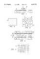
- FIG. 1shown is a cross-sectional representation of the cathode and substrate of the present invention.
- the cathodegenerally designated 10, comprises a resistive layer 11, a low effective work-function emitter layer 12 and an intermediate metal layer 13.
- the cathode 10sits on a cathode conductive layer 14 which, itself, sits on a substrate 15.
- the structure and function of the layers 11, 12, 13 of the cathode 10 and the relationship of the cathode 10 to conductive layer 14 and substrate 15are described in detail in related application Ser. No. 07/851,701, which is incorporated herein by reference.
- the emitter layer 12is, in the preferred embodiment of the present invention, amorphic diamond film comprising a plurality of diamond micro-crystallites in an overall amorphic structure.
- micro-crystallitesresult when the amorphic diamond material is deposited on the metal layer 13 by means of laser plasma deposition, chemical vapor deposition, ion beam deposition, sputtering, low temperature deposition (less than 500 degrees Centigrade), evaporation, cathodic arc evaporation, magnetically separated cathodic arc evaporation, laser acoustic wave deposition or similar techniques or a combination of the above whereby the amorphic diamond film is deposited as a plurality of micro-crystallites.
- laser plasma depositionchemical vapor deposition, ion beam deposition, sputtering, low temperature deposition (less than 500 degrees Centigrade), evaporation, cathodic arc evaporation, magnetically separated cathodic arc evaporation, laser acoustic wave deposition or similar techniques or a combination of the above whereby the amorphic diamond film is deposited as a plurality of micro-crystallites.
- micro-crystallitesform with certain atomic structures which depend on environmental conditions during deposition and somewhat on change. At a given environmental pressure and temperature, a certain percentage of crystals will emerge in an SP 2 (two-dimensional bonding of carbon atoms) configuration. A somewhat smaller percentage, however, will emerge in an SP 3 (three-dimensional bonding) configuration.
- the electron affinity for diamond micro-crystallites in an SP 3 configurationis less than that for carbon or graphite micro-crystallites in an SP 2 configuration. Therefore, micro-crystallites in the SP 3 configuration have a lower electron affinity, making them "emission sites.” These emission sites (or micro-crystallites with an SP 3 configuration) are represented in FIG. 2 as a plurality of black spots in the emitter layer 12.
- the flat surfaceis essentially a microscopically flat surface.
- a particular type of surface morphologyis not required. But, small features typical of any polycrystalline then film may improve emission characteristics because of an increase in enhancement factor. Certain micro-tip geometries may result in a larger enhancement factor and, in fact, the present invention could be used in a micro-tip or "peaked" structure.
- FIG. 3shown is a more detailed view of the micro-crystallites of FIG. 2. Shown is a plurality of micro-crystallites 31, 32, 33, 34, for example. Micro-crystallites 31, 32, 33 are shown as having an SP 2 configuration. Micro-crystallite 34 is shown as having an SP 3 configuration. As can be seen in FIG. 3, micro-crystallite 34 is surrounded by micro-crystallites having an SP 2 configuration.
- emission sitesThere are a very large number of randomly distributed localized emission sites per unit area of the surface. These emission sites are characterized by different electronic properties of that location from the rest of the film. This may be due to one or a combination of the following conditions:
- micro-crystallitesOne of the above conditions for creating differences in micro-crystallites is doping. Doping of amorphic diamond thin film can be accomplished by interjecting elemental carbon into the diamond as it is being deposited. When doping with carbon, micro-crystallites of different structures will be created statistically. Some micro-crystallites will be n-type. Alternatively, a non-carbon dopant atom could be used, depending upon the desired percentage and characteristics of emission sites. Fortunately, in the flat panel display environment, cathodes with as few as 1 emission site will function adequately. However, for optimal functioning, 1 to 10 n-type micro-crystallites per square micron are desired. And, in fact, the present invention results in micro-crystallites less than 1 micron in diameter, commonly 0.1 micron.
- Emission from the cathode 10 of FIG. 1occurs when a potential difference is impressed between the cathode 10 and an anode (not shown in FIG. 1) which is separated by some small distance from the cathode 10. Upon impression of this potential, electrons are caused to migrate to the emission layer 12 of the cathode 10.
- the condition that will be assumed to exist to create micro-crystallites of different work functionwill be a change in the bonding structure from SP 2 to SP 3 in the same micro-crystallite (condition 3 above).
- condition 3the emission sites shown in FIGS. 2 and 3
- micro-crystallites having an SP 3 configurationhave a lower work-function and electron affinity than micro-crystallites having an SP 2 configuration. Therefore, as voltage is increased between the cathode 10 and anode (not shown), the voltage will reach a point at which the SP 3 micro-crystallites will begin to emit electrons.
- SP 3 micro-crystallites on the surface of the cathode 10If the percentage of SP 3 micro-crystallites on the surface of the cathode 10 is sufficiently high, then emission from the SP 3 micro-crystallites will be sufficient to excite the anode (not shown), without having to raise voltage levels to a magnitude sufficient for emission to occur from the SP 2 micro-crystallites. Accordingly, the controlling pressure, temperature and method of deposition of the amorphic diamond film in a manner which is well-known in the art, SP 3 micro-crystallites can be made a large enough percentage of the total number of micro-crystallites to produce sufficient electron emission.
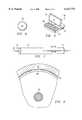
- FIG. 4shown is a cross-sectional view of a flat panel display employing the cathode of the present invention.
- the cathode 10still residing on its cathode conductive layer 14 and substrate 15 as in FIG. 1, has been mated to an anode, generally designated 41 and comprising a substrate 42, which in the preferred embodiment is glass.
- the substrate 42has an anode conductive layer 43 which, in the preferred embodiment, is an indium tin oxide layer.
- a phosphor layer 44is deposited on the anode conductive layer to provide a visual indication of electron flow from the cathode 10.
- a voltage source 47comprising a positive pole 48 and a negative pole 49.
- the positive poleis coupled from the source 47 to the anode conductive layer 43, while the negative pole 49 is coupled from the source 47 to the cathode conductive layer 14.
- the device 47impresses a potential difference between the cathode 10 and the anode 41, causing electron flow to occur between the cathode 10 and the anode 41 if the voltage impressed by the source 47 is sufficiently high.
- FIG. 9there is illustrated computer 90 with associated keyboard 93, disk drive 94, hardware 92 and display 91.
- the present inventionmay be employed within display 91 as a means for providing images and text. All that is visible of the present invention is anode 41.
- FIG. 5shown is a representation of a coated wire matrix emitter in the form of a wire mesh, generally designated 51.
- the wire mesh 51comprises a plurality of rows and columns of wire which are electrically joined at their intersection points.
- the wire mesh 51is then coated with a material having a low effective work-function and electron affinity, such as amorphic diamond, to thereby produce a wire mesh cathode for use in devices which previously used an uncoated wire or plate cathode and application of a high current and potential difference to produce incandescence and a flow of electrons from the mesh to an anode.
- amorphic diamond coating and its associated lower work functionincandescence is no longer necessary. Therefore, the wire mesh 51 cathode can be used at room temperature to emit electrons.
- FIG. 6shown is a cross-section of a wire which has been coated with a material having a low work-function and electron affinity.
- the wiredesignated 61, has a coating 62 which has been deposited by laser plasma deposition, or any one of the other well-known techniques listed above to thereby permit the coating 62 to act as a cold cathode in the same manner as the cathodes described in FIGS. 1-5.
- FIG. 7shown is one application of the wire 61 in which the coated wire 61 functions as a conductive filament and is surrounded by a glass tube 72, functioning as an anode and which has an electrical contact 73 to thereby produce a fluorescent tube.
- the tubefunctions in a manner which is analogous to the flat panel display application discussed in connection with FIGS. 1-5, that is, a potential difference is impressed between the wire 61 (negative) and the tube 72 sufficient to overcome the space-charge between the cathode wire 61 and the tube anode 72. Once the space-charge has been overcome, electrons will flow from emission site SP 3 micro-crystallites in the coating 62.
- FIG. 8shown is a partial section end view of the florescent tube 71 of FIG. 7. Shown again are the wire 61 and the coating 62 of FIG. 6 which, together, form a low effective work-function cathode in the fluorescent tube 71.
- the glass tube 72 of FIG. 7comprises a glass wall 81 on which is coated an anode conductive layer 82.
- the anode conductive layer 82is electrically coupled to the electrical contact 73 of FIG. 7.
- a phosphor layer 83is deposited on the anode conductive layer 82.
Landscapes
- Cathode-Ray Tubes And Fluorescent Screens For Display (AREA)
- Cold Cathode And The Manufacture (AREA)
Abstract
Description
This is a continuation of application Ser. No. 08/071,157 filed Jun. 2, 1993, abandoned, which is a continuation-in-part of application Ser. No. 07/851,701, filed Mar. 16, 1992, abandoned, and this is a continuation-in-part of application Ser. No. 08/456,453, filed Jun. 1, 1995, U.S. Pat. No. 5,763,997, which is a continuation-in-part of application Ser. No. 07/993,863, filed Dec. 23, 1992, abandoned, which is a continuation-in-part of application Ser. No. 07/851,701, filed Mar. 16, 1992, abandoned.
This invention relates, in general, to flat field emission cathodes and, more particularly, to such cathodes which employ an amorphic diamond film having a plurality of emission sites situated on a flat emission surface.
Field emission is a phenomenon which occurs when an electric field proximate the surface of an emission material marrows a width of a potential barrier existing at the surface of the emission material. This allows a quantum tunnelling effect to occur, whereby electrons cross through the potential barrier and are emitted from the material. This is as opposed to thermionic emission, whereby thermal energy within an emission material is sufficient to eject electrons from the material. Thermionic emission is a classical phenomenon, whereas filed emission is a quantum mechanical phenomenon.
The field strength required to initiate field emission of electrons from the surface of a particular material depends upon that material's effective "work function." Many materials have a positive work function and thus require a relatively intense electric field to bring about field emission. Some materials do, in fact, have a low work function, or even a negative electron affinity, and thus do not require intense fields for emission to occur. Such materials may be deposited as a thin film onto a conductor, resulting in a cathode with a relatively low threshold voltage required to produce electron emissions.
In prior art devices, it was desirable to enhance field emission of electrons by providing for a cathode geometry which focussed electron emission at a single, relatively sharp point at a tip of a conical cathode (called a micro-tip cathode). These micro-tip cathodes, in conjunction with extraction grids proximate the cathodes, have been in use for years in field emission displays.
For example, U.S. Pat. No. 4,857,799, which issued on Aug. 15, 1989, to Spindt et al., is directed to a matrix-addressed flat panel display using field emission cathodes. The cathodes are incorporated into the display backing structure, and energize corresponding cathodoluminescent areas on a face plate. The face plate is spaced 40 microns from the cathode arrangement in the preferred embodiment, and a vacuum is provided in the space between the plate and cathodes. Spacers in the form of legs interspersed among the pixels maintain the spacing, and electrical connections for the bases of the cathodes are diffused sections through the backing structure. Spindt et al. employ a plurality of micro-tip field emission cathodes in a matrix arrangement, the tips of the cathodes aligned with apertures in an extraction grid over the cathodes. With the addition of an anode over the extraction rid, the display described in Spindt et al. is a triode (three terminal) display.
Unfortunately, micro-tips employ a structure which is difficult to manufacture, since the micro-tips have fine geometries. Unless the micro-tips have a consistent geometry throughout the display, variations in emission from tip to tip will occur, resulting in unevenness in illumination of the display. Furthermore, since manufacturing tolerances are relatively tight, such micro-tip displays are expensive to make.
For years, others have directed substantial effort toward solving the problem of creating cathodes which can be mass manufactured to tight tolerances, allowing them to perform with accuracy and precision. Another object of some of these prior art inventions was that they made use of emission materials having a relatively low effective work function so as to minimize extraction field strength.
One such effort is documented in U.S. Pat. No. 3,947,716, which issued on Mar. 30, 1976, to Fraser, Jr. et al., directed to a field emission tip on which a metal adsorbent has been selectively deposited. In a vacuum, a clean field emission tip is subjected to heating pulses in the presence of an electrostatic field to create thermal field build up of a selected plane. Emission patterns from this selected plane are observed, and the process of heating the tip within the electrostatic field is repeated until emission is observed from the desired plane. The adsorbent is then evaporated onto the tip. The tip constructed by this process is selectively faceted with the emitting planar surface having a reduced work function and the non-emitting planar surface as having an increased work function. A metal adsorbent deposited on the tip so prepared results in afield emitter tip having substantially improved emission characteristics. Unfortunately, as previously mentioned, such micro-tip cathodes are expensive to produce due to their fine geometries. Also, since emission occurs from a relatively sharp tip, emission is still somewhat inconsistent from one cathode to another. Such disadvantages become intolerable when many cathodes are employed in great numbers such as in a flat panel display for a computer.
As is evident in the above-described cathode structure, an important attribute of good cathode design is to minimize the work function of the material constituting the cathode. In fact, some substances such as alkali metals and elemental carbon in the form of diamond crystals display a low effective work function. Many inventions have been directed to finding suitable geometries for cathodes employing negative electron affinity substances as a coating for the cathode.
For instance, U.S. Pat. No. 3,970,887, which issued on Jul. 20, 1976, to Smith et al., is directed to a microminiature field emission electron source and method of manufacturing the same wherein a single crystal semiconductor substrate is processed in accordance with known integrated microelectronic circuit techniques to produce a plurality of integral, single crystal semiconductor raised field emitter tips at desired field emission cathode sites on the surface of a substrate in a manner such that the field emitters tips are integral with the single crystal semiconductor substrate. An insulating layer and overlaying conductive layer may be formed in the order named over the semiconductor substrate and provided with openings at the field emission locations to form micro-anode structures for the field emitter tip. By initially appropriately doping the semiconductor substrate to provide opposite conductivity-type regions at each of the field emission locations and appropriately forming the conductive layer, electrical isolation between the several field emission locations can be obtained. Smith et al. call for a sharply-tipped cathode. Thus, the cathode disclosed in Smith et al. is subject to the same disadvantages as Fraser, Jr. et al.
U.S. Pat. No. 4,307,507, which issued on Dec. 29, 1981, to Gray et al., is directed to a method of manufacturing a field-emitter array cathode structure in which a substrate of single crystal material is selectively masked such that the unmasked areas define islands on the underlying substrate. The single crystal material under the unmasked areas is orientation-dependent etched to form an array of holes whose sides intersect at a crystal graphically sharp point.
U.S. Pat. No. 4,685,996, which issued on Aug. 11, 1987, to Busta et al., is also directed to a method of making a field emitter and includes an anisotropically etched single crystal silicon substrate to form at least one funnel-shaped protrusion on the substrate. The method of manufacturing disclosed in Busta et al. provides for a sharp-tipped cathode.
Sharp-tipped cathodes are further described in U.S. Pat. No. 4,885,636, which issued on Aug. 8, 1989, to Busta et al.
Yet another sharp-tipped emission cathode is disclosed in U.S. Pat. No. 4,964,946, which issued on Oct. 23, 1990, to Gray et al. Gray et al. disclose a process for fabricating soft-aligned field emitter arrays using a soft-leveling planarization technique, e.g. a spin-on process.
Even through they employ low effective work-function materials to advantage, sharp-tipped cathodes have fundamental problems when employed in a flat panel graphic display environment, as briefly mentioned above. First, they are relatively expensive to manufacture. Second, they are hard to manufacture with great consistency. That is, electron emission from sharp-tipped cathodes occurs at the tip. Therefore, the tip must be manufactured with extreme accuracy such that, in a matrix of adjacent cathodes, some cathodes do not emit electrons more efficiently than others, thereby creating an uneven visual display. In other words, the manufacturing of cathodes must be made more reliable so as to minimize the problem of inconsistencies in brightness in the display along its surface.
In Ser. No. 07/851,701, which was filed on Mar. 16, 1992, and entitled "Flat Panel Display Based on Diamond Thin Films," an alternative cathode structure was first disclosed. Ser. No. 07/851,701 discloses a cathode having a relatively flat emission surface as opposed to the aforementioned micro-tip configuration. The cathode, in its preferred embodiment, employs a field emission material having a relatively low effective work function. The material is deposited over a conductive layer and forms a plurality of emission sites, each of which can field-emit electrons in the presence of a relatively low intensity electric field.
Flat cathodes are much less expensive and difficult to produce in quantity because the fine, micro-tip geometry has been eliminated. The advantages of the flat cathode structure was discussed at length therein. The entirety of Ser. No. 07/851,701, which is commonly assigned with the present invention, is incorporated herein by reference.
A relatively recent development in the field of materials science has been the discovery of amorphic diamond. The structure and characteristics of amorphic diamond are discussed at length in "Thin-Film Diamond," published in the Texan Journal of Science, vol. 41, no. 4, 1989, by C. Collins et al. Collins et al. describe a method of producing amorphic diamond film by a laser deposition technique. As described therein, amorphic diamond comprises a plurality of micro-crystallites, each of which has a particular structure dependent upon the method of preparation of the film. The manner in which these micro-crystallites are formed and their particular properties are not entirely understood.
Diamond has a negative election affinity. That is, only a relatively low electric field is required to distort the potential barrier present at the surface of diamond. Thus, diamond is a very desirable material for use in conjunction with field emission cathodes. In fact, the prior art has employed crystalline diamond films to advantage as an emission surface on micro-tip cathodes.
In "Enhanced Cold-Cathode Emission Using Composite Resin-Carbon Coatings," published by S. Bajic and R. V. Latham from the department of electronic Engineering and Applied Physics, Aston University, Aston Triangle, Burmingham B4 7ET, United Kingdom, received May 29, 1987, a new type of composite resin-carbon field-emitting cathode is described which is found to switch on at applied fields as low as approximately 1.5 MV m-1, and subsequently has a reversible I-V characteristic with stable emission currents of > or =1 mA at moderate applied fields of typically < or =8 MV m-1. A direct electron emission imaging technique has shown that the total externally recorded current stems from a high density of individual emission sites randomly distributed over the cathode surface. The observed characteristics have been qualitatively explained by a new hot-electron emission mechanism involving a two-stage switch-on process associated with a metal-insulator-metal-insulator-vacuum (MIMIV) emitting regime. However, the mixing of the graphite powder into a resin compound results in larger grains, which results in fewer emission sites since the number of particles per unit area is small. It is preferred that a larger amount of sites be produced to produce a more uniform brightness from a low voltage source.
In "Cold Field Emission From CVD Diamond Films Observed In Emission Electron Microscopy," published by C. Wang, A. Garcia, D. C. Ingram, M. Lake and M. E. Kordesch from the Department of Physics and Astronomy and the condensed Matter and Surface Science Program at Ohio University, Athens, Ohio on Jun. 10, 1991, there is described thick chemical vapor deposited "CVD" polycrystalline diamond films having been observed to emit electrons with an intensity sufficient to form an image in the accelerating field of an emission microscope without external excitation. The individual crystallites are of the order of 1-10 microns. The CVD process requires 800° C. for the depositing of the diamond film. Such a temperature would melt a glass substrate.
The prior art has failed to: (1) take advantage of the unique properties of amorphic diamond; (2) provide for field emission cathodes having a more diffused area from which field emission can occur; and (3) provide for a high enough concentration of emission sites (i.e., smaller particles or crystallites) to produce a more uniform electron emission from each cathode site, yet require a low voltage source in order to produce the required field for the electron emissions.
The prior art has failed to recognize that amorphic diamond, which has physical qualities which differ substantially from other forms of diamond, makes a particularly good emission material. Ser. No. 07/851,701 was the first to disclose use of amorphic diamond film as an emission material. In fact, in the preferred embodiment of the invention described therein, amorphic diamond film was used in conjunction with a flat cathode structure to result in a radically different field emission cathode design.
The present invention takes the utilization of amorphic diamond a step further by depositing the amorphic diamond in such a manner so that a plurality of diamond micro-crystallite regions are deposited upon the cathode surface such that at each region (pixel) there are a certain percentage of the crystals emerging in an SP2 configuration and another percentage of the crystals emerging in an SP3 configuration. The numerous SP2 and SP3 configurations at each region result in numerous discontinuities or interface boundaries between the configurations, with the SP2 and SP3 crystallites having different electron affinities.
Accordingly, to take advantage of the above-noted opportunities, it is a primary object of the present invention to provide an independently addressable cathode, comprising a layer of conductive material and a layer of amorphic diamond film, functioning as a low effective work-function material, deposited over the conductive material, the amorphic diamond film comprising a plurality of distributed localized electron emission sites, each sub-site having a plurality of sub-regions with differing electron affinities between sub-regions.
In a preferred embodiment of the present invention, the amorphic diamond film is deposited as a relatively flat emission surface. Flat cathodes are easier and, therefore, less expensive to manufacture and, during operation of the display, are easier to control emission therefrom.
A technical advantage of the present invention is to provide a cathode wherein emission sites have electrical properties which include discontinuous boundaries with differing electron affinities.
Another technical advantage of the present invention is to provide a cathode wherein emission sites contain dopant atoms.
Yet another technical advantage of the present invention is to provide a cathode wherein a dopant atom is carbon.
Yet a further technical advantage of the present invention is to provide a cathode wherein emission sites each have a plurality of bonding structures.
Still yet another technical advantage of the present invention is to provide a cathode wherein one bonding structure at an emission site is SP3.
Still a further technical advantage of the present invention is to provide a cathode wherein each emission site has a plurality of bonding orders, one of which is SP3.
Another technical advantage of the present invention is to provide a cathode wherein emission sites contain dopants of an element different from a low effective work-function material. In the case of use of amorphic diamond as the low effective work-function material, the dopant element is other than carbon.
Still another technical advantage of the present invention is to provide a cathode wherein emission sites contain discontinuities in crystalline structure. The discontinuities are either point defects, line defects or dislocations.
The present invention further includes novel methods of operation for a flat panel display and use of amorphic diamond as a coating on an emissive wire screen and as an element within a cold cathode fluorescent lamp.
In the attainment of the above-noted features and advantages, the preferred embodiment of the present invention is an amorphic diamond film cold-cathode comprising a substrate, a layer of conductive material, an electronically resistive pillar deposited over the substrate and a layer of amorphic diamond film deposited over the conductive material, the amorphic diamond film having a relatively flat emission surface comprising a plurality of distributed micro-crystallite electron emission sites having differing electron affinities.
The foregoing has outlined rather broadly the features and technical advantages of the present invention in order that the detailed description of the invention that follows may be better understood. Additional features and advantages of the invention will be described hereinafter which form the subject of the claims of the invention. It should be appreciated by those skilled in the art that the conception and the specific embodiment disclosed may be readily utilized as a basis for modifying or designing other structures for carrying out the same purposes of the present invention. It should also be realized by those skilled in the art that such equivalent constructions do not depart from the spirit and scope of the invention as set forth in the appended claims.
For a more complete understanding of the present invention, and the advantages thereof, reference is now made to the following descriptions taken in conjunction with the accompanying drawings, in which:
FIG. 1 is a cross-sectional representation of the cathode and substrate of the present invention;
FIG. 2 is a top view of the cathode of the present invention including emission sites;
FIG. 3 is a more detailed representation of the emission sites of FIG. 2;
FIG. 4 is a cross-sectional view of a flat panel display employing the cathode of the present invention;
FIG. 5 is a representation of a coated wire matrix emitter;
FIG. 6 is a cross-sectional view of a coated wire;
FIG. 7 is a side view of a florescent tube employing the coated wire of FIG. 6;
FIG. 8 is a partial section end view of the fluorescent tube of FIG. 7; and
FIG. 9 is a computer with a flat-panel display that incorporates the present invention.
Turning now to FIG. 1, shown is a cross-sectional representation of the cathode and substrate of the present invention. The cathode, generally designated 10, comprises aresistive layer 11, a low effective work-function emitter layer 12 and anintermediate metal layer 13. Thecathode 10 sits on acathode conductive layer 14 which, itself, sits on asubstrate 15. The structure and function of thelayers cathode 10 and the relationship of thecathode 10 toconductive layer 14 andsubstrate 15 are described in detail in related application Ser. No. 07/851,701, which is incorporated herein by reference.
Turning now to FIG. 2, shown is a top view of thecathode 10 of FIG. 1. Theemitter layer 12 is, in the preferred embodiment of the present invention, amorphic diamond film comprising a plurality of diamond micro-crystallites in an overall amorphic structure. The micro-crystallites result when the amorphic diamond material is deposited on themetal layer 13 by means of laser plasma deposition, chemical vapor deposition, ion beam deposition, sputtering, low temperature deposition (less than 500 degrees Centigrade), evaporation, cathodic arc evaporation, magnetically separated cathodic arc evaporation, laser acoustic wave deposition or similar techniques or a combination of the above whereby the amorphic diamond film is deposited as a plurality of micro-crystallites. One such process is discussed within "Laser Plasma Source of Amorphic Diamond," published by the American Institute of Physics, January 1989, by C. B. Collins, et al.
The micro-crystallites form with certain atomic structures which depend on environmental conditions during deposition and somewhat on change. At a given environmental pressure and temperature, a certain percentage of crystals will emerge in an SP2 (two-dimensional bonding of carbon atoms) configuration. A somewhat smaller percentage, however, will emerge in an SP3 (three-dimensional bonding) configuration. The electron affinity for diamond micro-crystallites in an SP3 configuration is less than that for carbon or graphite micro-crystallites in an SP2 configuration. Therefore, micro-crystallites in the SP3 configuration have a lower electron affinity, making them "emission sites." These emission sites (or micro-crystallites with an SP3 configuration) are represented in FIG. 2 as a plurality of black spots in theemitter layer 12.
The flat surface is essentially a microscopically flat surface. A particular type of surface morphology, however, is not required. But, small features typical of any polycrystalline then film may improve emission characteristics because of an increase in enhancement factor. Certain micro-tip geometries may result in a larger enhancement factor and, in fact, the present invention could be used in a micro-tip or "peaked" structure.
Turning now to FIG. 3, shown is a more detailed view of the micro-crystallites of FIG. 2. Shown is a plurality ofmicro-crystallites
There are a very large number of randomly distributed localized emission sites per unit area of the surface. These emission sites are characterized by different electronic properties of that location from the rest of the film. This may be due to one or a combination of the following conditions:
1) presence of a doping atom (such as carbon) in the amorphic diamond lattice;
2) a change in the bonding structure from SP2 to SP3 in the same micro-crystallite;
3) a change in the order of the bonding structure in the same micro-crystallite;
4) an impurity (perhaps a dopant atom) of an element different from that of the film material;
5) an interface between the various micro-crystallites;
6) impurities or bonding structure differences occurring at the micro-crystallite boundary; or
7) other defects, such as point or line defects or dislocations.
The manner of creating each of the above conditions during production of the film is well known in the art.
One of the above conditions for creating differences in micro-crystallites is doping. Doping of amorphic diamond thin film can be accomplished by interjecting elemental carbon into the diamond as it is being deposited. When doping with carbon, micro-crystallites of different structures will be created statistically. Some micro-crystallites will be n-type. Alternatively, a non-carbon dopant atom could be used, depending upon the desired percentage and characteristics of emission sites. Fortunately, in the flat panel display environment, cathodes with as few as 1 emission site will function adequately. However, for optimal functioning, 1 to 10 n-type micro-crystallites per square micron are desired. And, in fact, the present invention results in micro-crystallites less than 1 micron in diameter, commonly 0.1 micron.
Emission from thecathode 10 of FIG. 1 occurs when a potential difference is impressed between thecathode 10 and an anode (not shown in FIG. 1) which is separated by some small distance from thecathode 10. Upon impression of this potential, electrons are caused to migrate to theemission layer 12 of thecathode 10.
In the example that follows, the condition that will be assumed to exist to create micro-crystallites of different work function will be a change in the bonding structure from SP2 to SP3 in the same micro-crystallite (condition 3 above). With respect to the emission sites shown in FIGS. 2 and 3, micro-crystallites having an SP3 configuration have a lower work-function and electron affinity than micro-crystallites having an SP2 configuration. Therefore, as voltage is increased between thecathode 10 and anode (not shown), the voltage will reach a point at which the SP3 micro-crystallites will begin to emit electrons. If the percentage of SP3 micro-crystallites on the surface of thecathode 10 is sufficiently high, then emission from the SP3 micro-crystallites will be sufficient to excite the anode (not shown), without having to raise voltage levels to a magnitude sufficient for emission to occur from the SP2 micro-crystallites. Accordingly, the controlling pressure, temperature and method of deposition of the amorphic diamond film in a manner which is well-known in the art, SP3 micro-crystallites can be made a large enough percentage of the total number of micro-crystallites to produce sufficient electron emission.
Turning now to FIG. 4, shown is a cross-sectional view of a flat panel display employing the cathode of the present invention. Thecathode 10, still residing on itscathode conductive layer 14 andsubstrate 15 as in FIG. 1, has been mated to an anode, generally designated 41 and comprising asubstrate 42, which in the preferred embodiment is glass. Thesubstrate 42 has an anodeconductive layer 43 which, in the preferred embodiment, is an indium tin oxide layer. Finally, aphosphor layer 44 is deposited on the anode conductive layer to provide a visual indication of electron flow from thecathode 10. In other words, when a potential difference is impressed between theanode 41 and thecathode 10, electrons flowing from thecathode 10 will flow toward the anodeconductive layer 43 but, upon striking thephosphor layer 44, will cause the phosphor layer to emit light through theglass substrate 42, thereby providing a visual display of a type desirable for use in conjunction with computers or other video equipment. Theanode 41 is separated by insulatingseparators cathode 10 and theanode 41. This is all in accordance with the device described in Ser. No. 07/851,701.
Further, in FIG. 4, represented is avoltage source 47 comprising apositive pole 48 and anegative pole 49. The positive pole is coupled from thesource 47 to the anodeconductive layer 43, while thenegative pole 49 is coupled from thesource 47 to thecathode conductive layer 14. Thedevice 47 impresses a potential difference between thecathode 10 and theanode 41, causing electron flow to occur between thecathode 10 and theanode 41 if the voltage impressed by thesource 47 is sufficiently high.
Turning now to FIG. 9, there is illustratedcomputer 90 with associatedkeyboard 93,disk drive 94,hardware 92 anddisplay 91. The present invention may be employed withindisplay 91 as a means for providing images and text. All that is visible of the present invention isanode 41.
Turning now to FIG. 5, shown is a representation of a coated wire matrix emitter in the form of a wire mesh, generally designated 51. Thewire mesh 51 comprises a plurality of rows and columns of wire which are electrically joined at their intersection points. Thewire mesh 51 is then coated with a material having a low effective work-function and electron affinity, such as amorphic diamond, to thereby produce a wire mesh cathode for use in devices which previously used an uncoated wire or plate cathode and application of a high current and potential difference to produce incandescence and a flow of electrons from the mesh to an anode. By virtue of the amorphic diamond coating and its associated lower work function, incandescence is no longer necessary. Therefore, thewire mesh 51 cathode can be used at room temperature to emit electrons.
Turning now to FIG. 6, shown is a cross-section of a wire which has been coated with a material having a low work-function and electron affinity. The wire, designated 61, has acoating 62 which has been deposited by laser plasma deposition, or any one of the other well-known techniques listed above to thereby permit thecoating 62 to act as a cold cathode in the same manner as the cathodes described in FIGS. 1-5.
Turning now to FIG. 7, shown is one application of thewire 61 in which thecoated wire 61 functions as a conductive filament and is surrounded by aglass tube 72, functioning as an anode and which has anelectrical contact 73 to thereby produce a fluorescent tube. The tube functions in a manner which is analogous to the flat panel display application discussed in connection with FIGS. 1-5, that is, a potential difference is impressed between the wire 61 (negative) and thetube 72 sufficient to overcome the space-charge between thecathode wire 61 and thetube anode 72. Once the space-charge has been overcome, electrons will flow from emission site SP3 micro-crystallites in thecoating 62.
Turning now to FIG. 8, shown is a partial section end view of theflorescent tube 71 of FIG. 7. Shown again are thewire 61 and thecoating 62 of FIG. 6 which, together, form a low effective work-function cathode in thefluorescent tube 71. Theglass tube 72 of FIG. 7 comprises aglass wall 81 on which is coated an anodeconductive layer 82. The anodeconductive layer 82 is electrically coupled to theelectrical contact 73 of FIG. 7. Finally, aphosphor layer 83 is deposited on the anodeconductive layer 82. When a potential difference is impressed between thecathode wire 61 and the anodeconductive layer 82, electrons are caused to flow between theemitter coating 82 and the anodeconductive layer 82. However, as in FIG. 4, the electrons strike thephosphor layer 83 first, causing thephosphor layer 83 to emit photons through thelass wall 81 and outside theflorescent tube 71, thereby providing light in a manner similar to conventional fluorescent tubes. However, because the fluorescent tube of FIGS. 7 and 8 employs a cathode having a low effective work-function emitter, such as amorphic diamond film, the fluorescent tube does not get warm during operation. Thus, the energy normally wasted in traditional fluorescent tubes in the form of heat is saved. In addition, since the heat is not produced, it need not be later removed by air conditioning.
Although the present invention and its advantages have been described in detail, it should be understood that various changes, substitutions and alterations can be made herein without departing from the spirit and scope of the invention as defined by the appended claims.
Claims (18)
1. A field emission cathode, comprising:
a layer of conductive material; and
a layer of amorphic diamond deposited over said conductive material, said amorphic diamond having a relatively flat emission surface operable for emitting electrons in response to an applied electric field.
2. The cathode as recited in claim 1 wherein said emission sites have electrical properties which are discontinuous from each other.
3. The cathode as recited in claim 1 wherein said emission sites each have a plurality of different bonding structures.
4. The cathode as recited in claim 3 wherein one of said bonding structures is SP3.
5. The cathode as recited in claim 1 wherein said emission sites each contain discontinuities in crystalline structure.
6. A diamond film cold-cathode, comprising:
a substrate;
a layer of conductive material disposed over said substrate; and
a layer of amorphic diamond film deposited over said conductive material, said amorphic diamond film comprising a plurality of micro-crystallite electron emission sites operable for emitting electrons in response to an applied electric field.
7. The cathode as recited in claim 6 wherein at least some adjacent ones of said emission sites have discontinuous electrical properties.
8. The cathode as recited in claim 6 wherein said emission surface is relatively flat.
9. The cathode as recited in claim 6 wherein said emission sites at said emission surface are relatively flat.
10. The cathode as recited in claim 6 wherein said sites have at least two different electron affinities.
11. The cathode as recited in claim 6 wherein each said site is under 1 micron in diameter.
12. The cathode as recited in claim 6 wherein each said site is less than or equal to 0.1 micron in diameter.
13. The cathode as recited in claim 6 wherein each of said emission sites have at least two different bonding structures.
14. The cathode as recited in claim 13 wherein one of said bonding structures is SP3.
15. The cathode as recited in claim 6 wherein said emission sites contain defects in crystalline structure.
16. The cathode as recited in claim 15 wherein said defects are point defects.
17. The cathode as recited in claim 15 wherein said defects are line defects.
18. The cathode as recited in claim 15 wherein said defects are dislocations.
Priority Applications (2)
| Application Number | Priority Date | Filing Date | Title |
|---|---|---|---|
| US08/868,644US6127773A (en) | 1992-03-16 | 1997-06-04 | Amorphic diamond film flat field emission cathode |
| US09/677,361US6573643B1 (en) | 1992-03-16 | 2000-10-02 | Field emission light source |
Applications Claiming Priority (5)
| Application Number | Priority Date | Filing Date | Title |
|---|---|---|---|
| US85170192A | 1992-03-16 | 1992-03-16 | |
| US99386392A | 1992-12-23 | 1992-12-23 | |
| US7115793A | 1993-06-02 | 1993-06-02 | |
| US08/456,453US5763997A (en) | 1992-03-16 | 1995-06-01 | Field emission display device |
| US08/868,644US6127773A (en) | 1992-03-16 | 1997-06-04 | Amorphic diamond film flat field emission cathode |
Related Parent Applications (2)
| Application Number | Title | Priority Date | Filing Date |
|---|---|---|---|
| US7115793AContinuation | 1992-03-16 | 1993-06-02 | |
| US08/456,453Continuation-In-PartUS5763997A (en) | 1992-03-16 | 1995-06-01 | Field emission display device |
Related Child Applications (1)
| Application Number | Title | Priority Date | Filing Date |
|---|---|---|---|
| US09/677,361Continuation-In-PartUS6573643B1 (en) | 1992-03-16 | 2000-10-02 | Field emission light source |
Publications (1)
| Publication Number | Publication Date |
|---|---|
| US6127773Atrue US6127773A (en) | 2000-10-03 |
Family
ID=27490879
Family Applications (1)
| Application Number | Title | Priority Date | Filing Date |
|---|---|---|---|
| US08/868,644Expired - Fee RelatedUS6127773A (en) | 1992-03-16 | 1997-06-04 | Amorphic diamond film flat field emission cathode |
Country Status (1)
| Country | Link |
|---|---|
| US (1) | US6127773A (en) |
Cited By (5)
| Publication number | Priority date | Publication date | Assignee | Title |
|---|---|---|---|---|
| US20020195962A1 (en)* | 1998-10-16 | 2002-12-26 | Si Diamond Technology, Inc. | Cold cathode |
| US6577045B1 (en)* | 1998-05-19 | 2003-06-10 | Alexandr Alexandrovich Blyablin | Cold-emission film-type cathode and method for producing the same |
| US6861790B1 (en)* | 1999-03-31 | 2005-03-01 | Honda Giken Kogyo Kabushiki Kaisha | Electronic element |
| CN100356495C (en)* | 2003-06-30 | 2007-12-19 | 宋健民 | Application device of amorphous diamond material |
| US7741764B1 (en) | 2007-01-09 | 2010-06-22 | Chien-Min Sung | DLC emitter devices and associated methods |
Citations (217)
| Publication number | Priority date | Publication date | Assignee | Title |
|---|---|---|---|---|
| US1954691A (en)* | 1930-09-27 | 1934-04-10 | Philips Nv | Process of making alpha layer containing alpha fluorescent material |
| US2851408A (en)* | 1954-10-01 | 1958-09-09 | Westinghouse Electric Corp | Method of electrophoretic deposition of luminescent materials and product resulting therefrom |
| US2867541A (en)* | 1957-02-25 | 1959-01-06 | Gen Electric | Method of preparing transparent luminescent screens |
| US2959483A (en)* | 1955-09-06 | 1960-11-08 | Zenith Radio Corp | Color image reproducer and method of manufacture |
| US3070441A (en)* | 1958-02-27 | 1962-12-25 | Rca Corp | Art of manufacturing cathode-ray tubes of the focus-mask variety |
| US3108904A (en)* | 1960-08-30 | 1963-10-29 | Gen Electric | Method of preparing luminescent materials and luminescent screens prepared thereby |
| US3259782A (en)* | 1961-11-08 | 1966-07-05 | Csf | Electron-emissive structure |
| US3314871A (en)* | 1962-12-20 | 1967-04-18 | Columbia Broadcasting Syst Inc | Method of cataphoretic deposition of luminescent materials |
| US3360450A (en)* | 1962-11-19 | 1967-12-26 | American Optical Corp | Method of making cathode ray tube face plates utilizing electrophoretic deposition |
| US3481733A (en)* | 1966-04-18 | 1969-12-02 | Sylvania Electric Prod | Method of forming a cathodo-luminescent screen |
| US3525679A (en)* | 1964-05-05 | 1970-08-25 | Westinghouse Electric Corp | Method of electrodepositing luminescent material on insulating substrate |
| FR2032436A2 (en) | 1969-02-27 | 1970-11-27 | Finanz Kompensations Anst | |
| US3554889A (en)* | 1968-11-22 | 1971-01-12 | Ibm | Color cathode ray tube screens |
| US3665241A (en)* | 1970-07-13 | 1972-05-23 | Stanford Research Inst | Field ionizer and field emission cathode structures and methods of production |
| US3675063A (en)* | 1970-01-02 | 1972-07-04 | Stanford Research Inst | High current continuous dynode electron multiplier |
| US3755704A (en)* | 1970-02-06 | 1973-08-28 | Stanford Research Inst | Field emission cathode structures and devices utilizing such structures |
| US3789471A (en)* | 1970-02-06 | 1974-02-05 | Stanford Research Inst | Field emission cathode structures, devices utilizing such structures, and methods of producing such structures |
| US3808048A (en)* | 1970-12-12 | 1974-04-30 | Philips Corp | Method of cataphoretically providing a uniform layer, and colour picture tube comprising such a layer |
| US3812559A (en)* | 1970-07-13 | 1974-05-28 | Stanford Research Inst | Methods of producing field ionizer and field emission cathode structures |
| US3855499A (en)* | 1972-02-25 | 1974-12-17 | Hitachi Ltd | Color display device |
| US3898146A (en)* | 1973-05-07 | 1975-08-05 | Gte Sylvania Inc | Process for fabricating a cathode ray tube screen structure |
| US3947716A (en)* | 1973-08-27 | 1976-03-30 | The United States Of America As Represented By The Secretary Of The Army | Field emission tip and process for making same |
| US3970887A (en)* | 1974-06-19 | 1976-07-20 | Micro-Bit Corporation | Micro-structure field emission electron source |
| US3998678A (en)* | 1973-03-22 | 1976-12-21 | Hitachi, Ltd. | Method of manufacturing thin-film field-emission electron source |
| US4008412A (en)* | 1974-08-16 | 1977-02-15 | Hitachi, Ltd. | Thin-film field-emission electron source and a method for manufacturing the same |
| US4075535A (en)* | 1975-04-15 | 1978-02-21 | Battelle Memorial Institute | Flat cathodic tube display |
| US4084942A (en)* | 1975-08-27 | 1978-04-18 | Villalobos Humberto Fernandez | Ultrasharp diamond edges and points and method of making |
| US4139773A (en)* | 1977-11-04 | 1979-02-13 | Oregon Graduate Center | Method and apparatus for producing bright high resolution ion beams |
| US4139733A (en)* | 1977-03-01 | 1979-02-13 | Bm-Elektronik Meletzky Kg | Electro acoustic transducer with improved diaphragm |
| US4141405A (en)* | 1977-07-27 | 1979-02-27 | Sri International | Method of fabricating a funnel-shaped miniature electrode for use as a field ionization source |
| US4143292A (en)* | 1975-06-27 | 1979-03-06 | Hitachi, Ltd. | Field emission cathode of glassy carbon and method of preparation |
| US4164680A (en)* | 1975-08-27 | 1979-08-14 | Villalobos Humberto F | Polycrystalline diamond emitter |
| US4168213A (en)* | 1976-04-29 | 1979-09-18 | U.S. Philips Corporation | Field emission device and method of forming same |
| US4178531A (en)* | 1977-06-15 | 1979-12-11 | Rca Corporation | CRT with field-emission cathode |
| US4307507A (en)* | 1980-09-10 | 1981-12-29 | The United States Of America As Represented By The Secretary Of The Navy | Method of manufacturing a field-emission cathode structure |
| US4350926A (en)* | 1980-07-28 | 1982-09-21 | The United States Of America As Represented By The Secretary Of The Army | Hollow beam electron source |
| US4482447A (en)* | 1982-09-14 | 1984-11-13 | Sony Corporation | Nonaqueous suspension for electrophoretic deposition of powders |
| US4498952A (en)* | 1982-09-17 | 1985-02-12 | Condesin, Inc. | Batch fabrication procedure for manufacture of arrays of field emitted electron beams with integral self-aligned optical lense in microguns |
| US4507562A (en)* | 1980-10-17 | 1985-03-26 | Jean Gasiot | Methods for rapidly stimulating luminescent phosphors and recovering information therefrom |
| US4513308A (en)* | 1982-09-23 | 1985-04-23 | The United States Of America As Represented By The Secretary Of The Navy | p-n Junction controlled field emitter array cathode |
| US4512912A (en)* | 1983-08-11 | 1985-04-23 | Kabushiki Kaisha Toshiba | White luminescent phosphor for use in cathode ray tube |
| US4528474A (en)* | 1982-03-05 | 1985-07-09 | Kim Jason J | Method and apparatus for producing an electron beam from a thermionic cathode |
| US4540983A (en)* | 1981-10-02 | 1985-09-10 | Futaba Denshi Kogyo K.K. | Fluorescent display device |
| US4542038A (en)* | 1983-09-30 | 1985-09-17 | Hitachi, Ltd. | Method of manufacturing cathode-ray tube |
| US4578614A (en)* | 1982-07-23 | 1986-03-25 | The United States Of America As Represented By The Secretary Of The Navy | Ultra-fast field emitter array vacuum integrated circuit switching device |
| US4588921A (en)* | 1981-01-31 | 1986-05-13 | International Standard Electric Corporation | Vacuum-fluorescent display matrix and method of operating same |
| US4594527A (en)* | 1983-10-06 | 1986-06-10 | Xerox Corporation | Vacuum fluorescent lamp having a flat geometry |
| US4633131A (en)* | 1984-12-12 | 1986-12-30 | North American Philips Corporation | Halo-reducing faceplate arrangement |
| US4647400A (en)* | 1983-06-23 | 1987-03-03 | Centre National De La Recherche Scientifique | Luminescent material or phosphor having a solid matrix within which is distributed a fluorescent compound, its preparation process and its use in a photovoltaic cell |
| US4663559A (en)* | 1982-09-17 | 1987-05-05 | Christensen Alton O | Field emission device |
| US4684353A (en)* | 1985-08-19 | 1987-08-04 | Dunmore Corporation | Flexible electroluminescent film laminate |
| US4684540A (en)* | 1986-01-31 | 1987-08-04 | Gte Products Corporation | Coated pigmented phosphors and process for producing same |
| US4685996A (en)* | 1986-10-14 | 1987-08-11 | Busta Heinz H | Method of making micromachined refractory metal field emitters |
| US4687825A (en)* | 1984-03-30 | 1987-08-18 | Kabushiki Kaisha Toshiba | Method of manufacturing phosphor screen of cathode ray tube |
| US4687938A (en)* | 1984-12-17 | 1987-08-18 | Hitachi, Ltd. | Ion source |
| US4710765A (en)* | 1983-07-30 | 1987-12-01 | Sony Corporation | Luminescent display device |
| US4721885A (en)* | 1987-02-11 | 1988-01-26 | Sri International | Very high speed integrated microelectronic tubes |
| US4728851A (en)* | 1982-01-08 | 1988-03-01 | Ford Motor Company | Field emitter device with gated memory |
| US4758449A (en)* | 1984-06-27 | 1988-07-19 | Matsushita Electronics Corporation | Method for making a phosphor layer |
| US4763187A (en)* | 1984-03-09 | 1988-08-09 | Laboratoire D'etude Des Surfaces | Method of forming images on a flat video screen |
| US4780684A (en)* | 1987-10-22 | 1988-10-25 | Hughes Aircraft Company | Microwave integrated distributed amplifier with field emission triodes |
| US4788472A (en)* | 1984-12-13 | 1988-11-29 | Nec Corporation | Fluoroescent display panel having indirectly-heated cathode |
| US4816717A (en)* | 1984-02-06 | 1989-03-28 | Rogers Corporation | Electroluminescent lamp having a polymer phosphor layer formed in substantially a non-crossed linked state |
| US4818914A (en)* | 1987-07-17 | 1989-04-04 | Sri International | High efficiency lamp |
| US4822466A (en)* | 1987-06-25 | 1989-04-18 | University Of Houston - University Park | Chemically bonded diamond films and method for producing same |
| US4827177A (en)* | 1986-09-08 | 1989-05-02 | The General Electric Company, P.L.C. | Field emission vacuum devices |
| US4835438A (en)* | 1986-11-27 | 1989-05-30 | Commissariat A L'energie Atomique | Source of spin polarized electrons using an emissive micropoint cathode |
| US4851254A (en)* | 1987-01-13 | 1989-07-25 | Nippon Soken, Inc. | Method and device for forming diamond film |
| US4855636A (en)* | 1987-10-08 | 1989-08-08 | Busta Heinz H | Micromachined cold cathode vacuum tube device and method of making |
| US4857161A (en)* | 1986-01-24 | 1989-08-15 | Commissariat A L'energie Atomique | Process for the production of a display means by cathodoluminescence excited by field emission |
| US4857799A (en)* | 1986-07-30 | 1989-08-15 | Sri International | Matrix-addressed flat panel display |
| US4874981A (en)* | 1988-05-10 | 1989-10-17 | Sri International | Automatically focusing field emission electrode |
| US4882659A (en)* | 1988-12-21 | 1989-11-21 | Delco Electronics Corporation | Vacuum fluorescent display having integral backlit graphic patterns |
| US4889690A (en)* | 1983-05-28 | 1989-12-26 | Max Planck Gesellschaft | Sensor for measuring physical parameters of concentration of particles |
| US4892757A (en)* | 1988-12-22 | 1990-01-09 | Gte Products Corporation | Method for a producing manganese activated zinc silicate phosphor |
| US4899081A (en)* | 1987-10-02 | 1990-02-06 | Futaba Denshi Kogyo K.K. | Fluorescent display device |
| US4900584A (en)* | 1987-01-12 | 1990-02-13 | Planar Systems, Inc. | Rapid thermal annealing of TFEL panels |
| US4908539A (en)* | 1984-07-24 | 1990-03-13 | Commissariat A L'energie Atomique | Display unit by cathodoluminescence excited by field emission |
| US4923421A (en)* | 1988-07-06 | 1990-05-08 | Innovative Display Development Partners | Method for providing polyimide spacers in a field emission panel display |
| US4926056A (en)* | 1988-06-10 | 1990-05-15 | Sri International | Microelectronic field ionizer and method of fabricating the same |
| US4933108A (en)* | 1978-04-13 | 1990-06-12 | Soeredal Sven G | Emitter for field emission and method of making same |
| US4940916A (en)* | 1987-11-06 | 1990-07-10 | Commissariat A L'energie Atomique | Electron source with micropoint emissive cathodes and display means by cathodoluminescence excited by field emission using said source |
| US4943343A (en)* | 1989-08-14 | 1990-07-24 | Zaher Bardai | Self-aligned gate process for fabricating field emitter arrays |
| US4956202A (en)* | 1988-12-22 | 1990-09-11 | Gte Products Corporation | Firing and milling method for producing a manganese activated zinc silicate phosphor |
| US4956574A (en)* | 1989-08-08 | 1990-09-11 | Motorola, Inc. | Switched anode field emission device |
| US4964946A (en)* | 1990-02-02 | 1990-10-23 | The United States Of America As Represented By The Secretary Of The Navy | Process for fabricating self-aligned field emitter arrays |
| US4987007A (en)* | 1988-04-18 | 1991-01-22 | Board Of Regents, The University Of Texas System | Method and apparatus for producing a layer of material from a laser ion source |
| US4990416A (en)* | 1989-06-19 | 1991-02-05 | Coloray Display Corporation | Deposition of cathodoluminescent materials by reversal toning |
| US4990766A (en)* | 1989-05-22 | 1991-02-05 | Murasa International | Solid state electron amplifier |
| US4994205A (en)* | 1989-02-03 | 1991-02-19 | Eastman Kodak Company | Composition containing a hafnia phosphor of enhanced luminescence |
| US5007873A (en)* | 1990-02-09 | 1991-04-16 | Motorola, Inc. | Non-planar field emission device having an emitter formed with a substantially normal vapor deposition process |
| US5015912A (en)* | 1986-07-30 | 1991-05-14 | Sri International | Matrix-addressed flat panel display |
| US5019003A (en)* | 1989-09-29 | 1991-05-28 | Motorola, Inc. | Field emission device having preformed emitters |
| US5036247A (en)* | 1985-09-10 | 1991-07-30 | Pioneer Electronic Corporation | Dot matrix fluorescent display device |
| US5038070A (en)* | 1989-12-26 | 1991-08-06 | Hughes Aircraft Company | Field emitter structure and fabrication process |
| US5043715A (en)* | 1988-12-07 | 1991-08-27 | Westinghouse Electric Corp. | Thin film electroluminescent edge emitter structure with optical lens and multi-color light emission systems |
| US5054046A (en)* | 1988-01-06 | 1991-10-01 | Jupiter Toy Company | Method of and apparatus for production and manipulation of high density charge |
| US5054047A (en)* | 1988-01-06 | 1991-10-01 | Jupiter Toy Company | Circuits responsive to and controlling charged particles |
| US5055744A (en)* | 1987-12-01 | 1991-10-08 | Futuba Denshi Kogyo K.K. | Display device |
| US5055077A (en)* | 1989-11-22 | 1991-10-08 | Motorola, Inc. | Cold cathode field emission device having an electrode in an encapsulating layer |
| US5057047A (en)* | 1990-09-27 | 1991-10-15 | The United States Of America As Represented By The Secretary Of The Navy | Low capacitance field emitter array and method of manufacture therefor |
| US5063327A (en) | 1988-07-06 | 1991-11-05 | Coloray Display Corporation | Field emission cathode based flat panel display having polyimide spacers |
| US5063323A (en) | 1990-07-16 | 1991-11-05 | Hughes Aircraft Company | Field emitter structure providing passageways for venting of outgassed materials from active electronic area |
| US5064396A (en) | 1990-01-29 | 1991-11-12 | Coloray Display Corporation | Method of manufacturing an electric field producing structure including a field emission cathode |
| US5066883A (en) | 1987-07-15 | 1991-11-19 | Canon Kabushiki Kaisha | Electron-emitting device with electron-emitting region insulated from electrodes |
| US5075595A (en) | 1991-01-24 | 1991-12-24 | Motorola, Inc. | Field emission device with vertically integrated active control |
| US5075596A (en) | 1990-10-02 | 1991-12-24 | United Technologies Corporation | Electroluminescent display brightness compensation |
| US5075591A (en) | 1990-07-13 | 1991-12-24 | Coloray Display Corporation | Matrix addressing arrangement for a flat panel display with field emission cathodes |
| US5079476A (en) | 1990-02-09 | 1992-01-07 | Motorola, Inc. | Encapsulated field emission device |
| US5085958A (en) | 1989-08-30 | 1992-02-04 | Samsung Electron Devices Co., Ltd. | Manufacturing method of phosphor film of cathode ray tube |
| US5089292A (en) | 1990-07-20 | 1992-02-18 | Coloray Display Corporation | Field emission cathode array coated with electron work function reducing material, and method |
| US5089742A (en) | 1990-09-28 | 1992-02-18 | The United States Of America As Represented By The Secretary Of The Navy | Electron beam source formed with biologically derived tubule materials |
| US5089812A (en) | 1988-02-26 | 1992-02-18 | Casio Computer Co., Ltd. | Liquid-crystal display |
| US5090932A (en) | 1988-03-25 | 1992-02-25 | Thomson-Csf | Method for the fabrication of field emission type sources, and application thereof to the making of arrays of emitters |
| US5098737A (en) | 1988-04-18 | 1992-03-24 | Board Of Regents The University Of Texas System | Amorphic diamond material produced by laser plasma deposition |
| US5101288A (en) | 1989-04-06 | 1992-03-31 | Ricoh Company, Ltd. | LCD having obliquely split or interdigitated pixels connected to MIM elements having a diamond-like insulator |
| US5101137A (en) | 1989-07-10 | 1992-03-31 | Westinghouse Electric Corp. | Integrated tfel flat panel face and edge emitter structure producing multiple light sources |
| US5103144A (en) | 1990-10-01 | 1992-04-07 | Raytheon Company | Brightness control for flat panel display |
| US5103145A (en) | 1990-09-05 | 1992-04-07 | Raytheon Company | Luminance control for cathode-ray tube having field emission cathode |
| US5117299A (en) | 1989-05-20 | 1992-05-26 | Ricoh Company, Ltd. | Liquid crystal display with a light blocking film of hard carbon |
| US5117267A (en) | 1989-09-27 | 1992-05-26 | Sumitomo Electric Industries, Ltd. | Semiconductor heterojunction structure |
| US5119386A (en) | 1989-01-17 | 1992-06-02 | Matsushita Electric Industrial Co., Ltd. | Light emitting device |
| US5123039A (en) | 1988-01-06 | 1992-06-16 | Jupiter Toy Company | Energy conversion using high charge density |
| US5124558A (en) | 1985-10-10 | 1992-06-23 | Quantex Corporation | Imaging system for mamography employing electron trapping materials |
| US5124072A (en) | 1991-12-02 | 1992-06-23 | General Electric Company | Alkaline earth hafnate phosphor with cerium luminescence |
| US5126287A (en) | 1990-06-07 | 1992-06-30 | Mcnc | Self-aligned electron emitter fabrication method and devices formed thereby |
| US5129850A (en) | 1991-08-20 | 1992-07-14 | Motorola, Inc. | Method of making a molded field emission electron emitter employing a diamond coating |
| US5132585A (en) | 1990-12-21 | 1992-07-21 | Motorola, Inc. | Projection display faceplate employing an optically transmissive diamond coating of high thermal conductivity |
| US5132676A (en) | 1989-05-24 | 1992-07-21 | Ricoh Company, Ltd. | Liquid crystal display |
| US5138237A (en) | 1991-08-20 | 1992-08-11 | Motorola, Inc. | Field emission electron device employing a modulatable diamond semiconductor emitter |
| US5136764A (en) | 1990-09-27 | 1992-08-11 | Motorola, Inc. | Method for forming a field emission device |
| US5140219A (en) | 1991-02-28 | 1992-08-18 | Motorola, Inc. | Field emission display device employing an integral planar field emission control device |
| US5141459A (en) | 1990-07-18 | 1992-08-25 | International Business Machines Corporation | Structures and processes for fabricating field emission cathodes |
| US5142184A (en) | 1990-02-09 | 1992-08-25 | Kane Robert C | Cold cathode field emission device with integral emitter ballasting |
| US5142256A (en) | 1991-04-04 | 1992-08-25 | Motorola, Inc. | Pin diode with field emission device switch |
| US5142390A (en) | 1989-02-23 | 1992-08-25 | Ricoh Company, Ltd. | MIM element with a doped hard carbon film |
| US5141460A (en) | 1991-08-20 | 1992-08-25 | Jaskie James E | Method of making a field emission electron source employing a diamond coating |
| US5144191A (en) | 1991-06-12 | 1992-09-01 | Mcnc | Horizontal microelectronic field emission devices |
| US5148078A (en) | 1990-08-29 | 1992-09-15 | Motorola, Inc. | Field emission device employing a concentric post |
| US5148461A (en) | 1988-01-06 | 1992-09-15 | Jupiter Toy Co. | Circuits responsive to and controlling charged particles |
| US5150192A (en) | 1990-09-27 | 1992-09-22 | The United States Of America As Represented By The Secretary Of The Navy | Field emitter array |
| US5150011A (en) | 1990-03-30 | 1992-09-22 | Matsushita Electronics Corporation | Gas discharge display device |
| US5151061A (en) | 1992-02-21 | 1992-09-29 | Micron Technology, Inc. | Method to form self-aligned tips for flat panel displays |
| US5153901A (en) | 1988-01-06 | 1992-10-06 | Jupiter Toy Company | Production and manipulation of charged particles |
| US5153753A (en) | 1989-04-12 | 1992-10-06 | Ricoh Company, Ltd. | Active matrix-type liquid crystal display containing a horizontal MIM device with inter-digital conductors |
| US5155420A (en) | 1991-08-05 | 1992-10-13 | Smith Robert T | Switching circuits employing field emission devices |
| US5157304A (en) | 1990-12-17 | 1992-10-20 | Motorola, Inc. | Field emission device display with vacuum seal |
| US5157309A (en) | 1990-09-13 | 1992-10-20 | Motorola Inc. | Cold-cathode field emission device employing a current source means |
| US5156770A (en) | 1990-06-26 | 1992-10-20 | Thomson Consumer Electronics, Inc. | Conductive contact patch for a CRT faceplate panel |
| US5162704A (en) | 1991-02-06 | 1992-11-10 | Futaba Denshi Kogyo K.K. | Field emission cathode |
| US5166456A (en) | 1985-12-16 | 1992-11-24 | Kasei Optonix, Ltd. | Luminescent phosphor composition |
| US5173634A (en) | 1990-11-30 | 1992-12-22 | Motorola, Inc. | Current regulated field-emission device |
| US5173635A (en) | 1990-11-30 | 1992-12-22 | Motorola, Inc. | Bi-directional field emission device |
| US5173697A (en) | 1992-02-05 | 1992-12-22 | Motorola, Inc. | Digital-to-analog signal conversion device employing scaled field emission devices |
| US5180951A (en) | 1992-02-05 | 1993-01-19 | Motorola, Inc. | Electron device electron source including a polycrystalline diamond |
| US5183529A (en) | 1990-10-29 | 1993-02-02 | Ford Motor Company | Fabrication of polycrystalline free-standing diamond films |
| US5185178A (en) | 1988-08-29 | 1993-02-09 | Minnesota Mining And Manufacturing Company | Method of forming an array of densely packed discrete metal microspheres |
| US5187578A (en) | 1990-03-02 | 1993-02-16 | Hitachi, Ltd. | Tone display method and apparatus reducing flicker |
| US5186670A (en) | 1992-03-02 | 1993-02-16 | Micron Technology, Inc. | Method to form self-aligned gate structures and focus rings |
| US5191217A (en) | 1991-11-25 | 1993-03-02 | Motorola, Inc. | Method and apparatus for field emission device electrostatic electron beam focussing |
| US5192240A (en) | 1990-02-22 | 1993-03-09 | Seiko Epson Corporation | Method of manufacturing a microelectronic vacuum device |
| US5194780A (en) | 1990-06-13 | 1993-03-16 | Commissariat A L'energie Atomique | Electron source with microtip emissive cathodes |
| US5199917A (en) | 1991-12-09 | 1993-04-06 | Cornell Research Foundation, Inc. | Silicon tip field emission cathode arrays and fabrication thereof |
| US5199918A (en) | 1991-11-07 | 1993-04-06 | Microelectronics And Computer Technology Corporation | Method of forming field emitter device with diamond emission tips |
| US5201992A (en) | 1990-07-12 | 1993-04-13 | Bell Communications Research, Inc. | Method for making tapered microminiature silicon structures |
| US5202571A (en) | 1990-07-06 | 1993-04-13 | Canon Kabushiki Kaisha | Electron emitting device with diamond |
| US5204581A (en) | 1990-07-12 | 1993-04-20 | Bell Communications Research, Inc. | Device including a tapered microminiature silicon structure |
| US5204021A (en) | 1992-01-03 | 1993-04-20 | General Electric Company | Lanthanide oxide fluoride phosphor having cerium luminescence |
| US5203731A (en) | 1990-07-18 | 1993-04-20 | International Business Machines Corporation | Process and structure of an integrated vacuum microelectronic device |
| US5205770A (en) | 1992-03-12 | 1993-04-27 | Micron Technology, Inc. | Method to form high aspect ratio supports (spacers) for field emission display using micro-saw technology |
| US5210462A (en) | 1990-12-28 | 1993-05-11 | Sony Corporation | Flat panel display apparatus and a method of manufacturing thereof |
| US5210430A (en) | 1988-12-27 | 1993-05-11 | Canon Kabushiki Kaisha | Electric field light-emitting device |
| US5209687A (en) | 1990-12-28 | 1993-05-11 | Sony Corporation | Flat panel display apparatus and a method of manufacturing thereof |
| US5212426A (en) | 1991-01-24 | 1993-05-18 | Motorola, Inc. | Integrally controlled field emission flat display device |
| US5214416A (en) | 1989-12-01 | 1993-05-25 | Ricoh Company, Ltd. | Active matrix board |
| US5214347A (en) | 1990-06-08 | 1993-05-25 | The United States Of America As Represented By The Secretary Of The Navy | Layered thin-edged field-emitter device |
| US5214346A (en) | 1990-02-22 | 1993-05-25 | Seiko Epson Corporation | Microelectronic vacuum field emission device |
| US5213712A (en) | 1992-02-10 | 1993-05-25 | General Electric Company | Lanthanum lutetium oxide phosphor with cerium luminescence |
| US5220725A (en) | 1991-04-09 | 1993-06-22 | Northeastern University | Micro-emitter-based low-contact-force interconnection device |
| US5227699A (en) | 1991-08-16 | 1993-07-13 | Amoco Corporation | Recessed gate field emission |
| US5228877A (en) | 1991-01-25 | 1993-07-20 | Gec-Marconi Limited | Field emission devices |
| US5229682A (en) | 1989-12-18 | 1993-07-20 | Seiko Epson Corporation | Field electron emission device |
| US5229331A (en) | 1992-02-14 | 1993-07-20 | Micron Technology, Inc. | Method to form self-aligned gate structures around cold cathode emitter tips using chemical mechanical polishing technology |
| US5228878A (en) | 1989-12-18 | 1993-07-20 | Seiko Epson Corporation | Field electron emission device production method |
| US5231606A (en) | 1990-07-02 | 1993-07-27 | The United States Of America As Represented By The Secretary Of The Navy | Field emitter array memory device |
| US5233263A (en) | 1991-06-27 | 1993-08-03 | International Business Machines Corporation | Lateral field emission devices |
| US5235244A (en) | 1990-01-29 | 1993-08-10 | Innovative Display Development Partners | Automatically collimating electron beam producing arrangement |
| US5243252A (en) | 1989-12-19 | 1993-09-07 | Matsushita Electric Industrial Co., Ltd. | Electron field emission device |
| US5242620A (en) | 1992-07-02 | 1993-09-07 | General Electric Company | Gadolinium lutetium aluminate phosphor with cerium luminescence |
| US5250451A (en) | 1991-04-23 | 1993-10-05 | France Telecom Etablissement Autonome De Droit Public | Process for the production of thin film transistors |
| US5252833A (en) | 1992-02-05 | 1993-10-12 | Motorola, Inc. | Electron source for depletion mode electron emission apparatus |
| US5256888A (en) | 1992-05-04 | 1993-10-26 | Motorola, Inc. | Transistor device apparatus employing free-space electron emission from a diamond material surface |
| US5259799A (en) | 1992-03-02 | 1993-11-09 | Micron Technology, Inc. | Method to form self-aligned gate structures and focus rings |
| US5262698A (en) | 1991-10-31 | 1993-11-16 | Raytheon Company | Compensation for field emission display irregularities |
| US5266155A (en) | 1990-06-08 | 1993-11-30 | The United States Of America As Represented By The Secretary Of The Navy | Method for making a symmetrical layered thin film edge field-emitter-array |
| US5276521A (en) | 1990-07-30 | 1994-01-04 | Olympus Optical Co., Ltd. | Solid state imaging device having a constant pixel integrating period and blooming resistance |
| US5277638A (en) | 1992-04-29 | 1994-01-11 | Samsung Electron Devices Co., Ltd. | Method for manufacturing field emission display |
| US5278475A (en) | 1992-06-01 | 1994-01-11 | Motorola, Inc. | Cathodoluminescent display apparatus and method for realization using diamond crystallites |
| US5281891A (en) | 1991-02-22 | 1994-01-25 | Matsushita Electric Industrial Co., Ltd. | Electron emission element |
| US5283501A (en) | 1991-07-18 | 1994-02-01 | Motorola, Inc. | Electron device employing a low/negative electron affinity electron source |
| US5283500A (en) | 1992-05-28 | 1994-02-01 | At&T Bell Laboratories | Flat panel field emission display apparatus |
| US5285129A (en) | 1988-05-31 | 1994-02-08 | Canon Kabushiki Kaisha | Segmented electron emission device |
| US5296117A (en) | 1991-12-11 | 1994-03-22 | Agfa-Gevaert, N.V. | Method for the production of a radiographic screen |
| US5302423A (en) | 1993-07-09 | 1994-04-12 | Minnesota Mining And Manufacturing Company | Method for fabricating pixelized phosphors |
| US5312514A (en) | 1991-11-07 | 1994-05-17 | Microelectronics And Computer Technology Corporation | Method of making a field emitter device using randomly located nuclei as an etch mask |
| US5347201A (en) | 1991-02-25 | 1994-09-13 | Panocorp Display Systems | Display device |
| US5378963A (en) | 1991-03-06 | 1995-01-03 | Sony Corporation | Field emission type flat display apparatus |
| US5399238A (en) | 1991-11-07 | 1995-03-21 | Microelectronics And Computer Technology Corporation | Method of making field emission tips using physical vapor deposition of random nuclei as etch mask |
| US5412285A (en) | 1990-12-06 | 1995-05-02 | Seiko Epson Corporation | Linear amplifier incorporating a field emission device having specific gap distances between gate and cathode |
| US5430347A (en) | 1991-11-29 | 1995-07-04 | Motorola, Inc. | Field emission device with integrally formed electrostatic lens |
| US5432407A (en) | 1990-12-26 | 1995-07-11 | Motorola, Inc. | Field emission device as charge transport switch for energy storage network |
| US5432003A (en) | 1988-10-03 | 1995-07-11 | Crystallume | Continuous thin diamond film and method for making same |
| US5439705A (en) | 1990-04-25 | 1995-08-08 | Minnesota Mining And Manufacturing Company | Encapsulated electroluminescent phosphor and method for making same |
| US5449970A (en) | 1992-03-16 | 1995-09-12 | Microelectronics And Computer Technology Corporation | Diode structure flat panel display |
| US5536193A (en) | 1991-11-07 | 1996-07-16 | Microelectronics And Computer Technology Corporation | Method of making wide band gap field emitter |
| US5675216A (en) | 1992-03-16 | 1997-10-07 | Microelectronics And Computer Technololgy Corp. | Amorphic diamond film flat field emission cathode |
| US5686791A (en) | 1992-03-16 | 1997-11-11 | Microelectronics And Computer Technology Corp. | Amorphic diamond film flat field emission cathode |
- 1997
- 1997-06-04USUS08/868,644patent/US6127773A/ennot_activeExpired - Fee Related
Patent Citations (223)
| Publication number | Priority date | Publication date | Assignee | Title |
|---|---|---|---|---|
| US1954691A (en)* | 1930-09-27 | 1934-04-10 | Philips Nv | Process of making alpha layer containing alpha fluorescent material |
| US2851408A (en)* | 1954-10-01 | 1958-09-09 | Westinghouse Electric Corp | Method of electrophoretic deposition of luminescent materials and product resulting therefrom |
| US2959483A (en)* | 1955-09-06 | 1960-11-08 | Zenith Radio Corp | Color image reproducer and method of manufacture |
| US2867541A (en)* | 1957-02-25 | 1959-01-06 | Gen Electric | Method of preparing transparent luminescent screens |
| US3070441A (en)* | 1958-02-27 | 1962-12-25 | Rca Corp | Art of manufacturing cathode-ray tubes of the focus-mask variety |
| US3108904A (en)* | 1960-08-30 | 1963-10-29 | Gen Electric | Method of preparing luminescent materials and luminescent screens prepared thereby |
| US3259782A (en)* | 1961-11-08 | 1966-07-05 | Csf | Electron-emissive structure |
| US3360450A (en)* | 1962-11-19 | 1967-12-26 | American Optical Corp | Method of making cathode ray tube face plates utilizing electrophoretic deposition |
| US3314871A (en)* | 1962-12-20 | 1967-04-18 | Columbia Broadcasting Syst Inc | Method of cataphoretic deposition of luminescent materials |
| US3525679A (en)* | 1964-05-05 | 1970-08-25 | Westinghouse Electric Corp | Method of electrodepositing luminescent material on insulating substrate |
| US3481733A (en)* | 1966-04-18 | 1969-12-02 | Sylvania Electric Prod | Method of forming a cathodo-luminescent screen |
| US3554889A (en)* | 1968-11-22 | 1971-01-12 | Ibm | Color cathode ray tube screens |
| FR2032436A2 (en) | 1969-02-27 | 1970-11-27 | Finanz Kompensations Anst | |
| US3675063A (en)* | 1970-01-02 | 1972-07-04 | Stanford Research Inst | High current continuous dynode electron multiplier |
| US3789471A (en)* | 1970-02-06 | 1974-02-05 | Stanford Research Inst | Field emission cathode structures, devices utilizing such structures, and methods of producing such structures |
| US3755704A (en)* | 1970-02-06 | 1973-08-28 | Stanford Research Inst | Field emission cathode structures and devices utilizing such structures |
| US3812559A (en)* | 1970-07-13 | 1974-05-28 | Stanford Research Inst | Methods of producing field ionizer and field emission cathode structures |
| US3665241A (en)* | 1970-07-13 | 1972-05-23 | Stanford Research Inst | Field ionizer and field emission cathode structures and methods of production |
| US3808048A (en)* | 1970-12-12 | 1974-04-30 | Philips Corp | Method of cataphoretically providing a uniform layer, and colour picture tube comprising such a layer |
| US3855499A (en)* | 1972-02-25 | 1974-12-17 | Hitachi Ltd | Color display device |
| US3998678A (en)* | 1973-03-22 | 1976-12-21 | Hitachi, Ltd. | Method of manufacturing thin-film field-emission electron source |
| US3898146A (en)* | 1973-05-07 | 1975-08-05 | Gte Sylvania Inc | Process for fabricating a cathode ray tube screen structure |
| US3947716A (en)* | 1973-08-27 | 1976-03-30 | The United States Of America As Represented By The Secretary Of The Army | Field emission tip and process for making same |
| US3970887A (en)* | 1974-06-19 | 1976-07-20 | Micro-Bit Corporation | Micro-structure field emission electron source |
| US4008412A (en)* | 1974-08-16 | 1977-02-15 | Hitachi, Ltd. | Thin-film field-emission electron source and a method for manufacturing the same |
| US4075535A (en)* | 1975-04-15 | 1978-02-21 | Battelle Memorial Institute | Flat cathodic tube display |
| US4143292A (en)* | 1975-06-27 | 1979-03-06 | Hitachi, Ltd. | Field emission cathode of glassy carbon and method of preparation |
| US4084942A (en)* | 1975-08-27 | 1978-04-18 | Villalobos Humberto Fernandez | Ultrasharp diamond edges and points and method of making |
| US4164680A (en)* | 1975-08-27 | 1979-08-14 | Villalobos Humberto F | Polycrystalline diamond emitter |
| US4168213A (en)* | 1976-04-29 | 1979-09-18 | U.S. Philips Corporation | Field emission device and method of forming same |
| US4139733A (en)* | 1977-03-01 | 1979-02-13 | Bm-Elektronik Meletzky Kg | Electro acoustic transducer with improved diaphragm |
| US4178531A (en)* | 1977-06-15 | 1979-12-11 | Rca Corporation | CRT with field-emission cathode |
| US4141405A (en)* | 1977-07-27 | 1979-02-27 | Sri International | Method of fabricating a funnel-shaped miniature electrode for use as a field ionization source |
| US4139773A (en)* | 1977-11-04 | 1979-02-13 | Oregon Graduate Center | Method and apparatus for producing bright high resolution ion beams |
| US4933108A (en)* | 1978-04-13 | 1990-06-12 | Soeredal Sven G | Emitter for field emission and method of making same |
| US4350926A (en)* | 1980-07-28 | 1982-09-21 | The United States Of America As Represented By The Secretary Of The Army | Hollow beam electron source |
| US4307507A (en)* | 1980-09-10 | 1981-12-29 | The United States Of America As Represented By The Secretary Of The Navy | Method of manufacturing a field-emission cathode structure |
| US4507562A (en)* | 1980-10-17 | 1985-03-26 | Jean Gasiot | Methods for rapidly stimulating luminescent phosphors and recovering information therefrom |
| US4588921A (en)* | 1981-01-31 | 1986-05-13 | International Standard Electric Corporation | Vacuum-fluorescent display matrix and method of operating same |
| US4540983A (en)* | 1981-10-02 | 1985-09-10 | Futaba Denshi Kogyo K.K. | Fluorescent display device |
| US4728851A (en)* | 1982-01-08 | 1988-03-01 | Ford Motor Company | Field emitter device with gated memory |
| US4528474A (en)* | 1982-03-05 | 1985-07-09 | Kim Jason J | Method and apparatus for producing an electron beam from a thermionic cathode |
| US4578614A (en)* | 1982-07-23 | 1986-03-25 | The United States Of America As Represented By The Secretary Of The Navy | Ultra-fast field emitter array vacuum integrated circuit switching device |
| US4482447A (en)* | 1982-09-14 | 1984-11-13 | Sony Corporation | Nonaqueous suspension for electrophoretic deposition of powders |
| US4498952A (en)* | 1982-09-17 | 1985-02-12 | Condesin, Inc. | Batch fabrication procedure for manufacture of arrays of field emitted electron beams with integral self-aligned optical lense in microguns |
| US4663559A (en)* | 1982-09-17 | 1987-05-05 | Christensen Alton O | Field emission device |
| US4513308A (en)* | 1982-09-23 | 1985-04-23 | The United States Of America As Represented By The Secretary Of The Navy | p-n Junction controlled field emitter array cathode |
| US4889690A (en)* | 1983-05-28 | 1989-12-26 | Max Planck Gesellschaft | Sensor for measuring physical parameters of concentration of particles |
| US4647400A (en)* | 1983-06-23 | 1987-03-03 | Centre National De La Recherche Scientifique | Luminescent material or phosphor having a solid matrix within which is distributed a fluorescent compound, its preparation process and its use in a photovoltaic cell |
| US4710765A (en)* | 1983-07-30 | 1987-12-01 | Sony Corporation | Luminescent display device |
| US4512912A (en)* | 1983-08-11 | 1985-04-23 | Kabushiki Kaisha Toshiba | White luminescent phosphor for use in cathode ray tube |
| US4542038A (en)* | 1983-09-30 | 1985-09-17 | Hitachi, Ltd. | Method of manufacturing cathode-ray tube |
| US4594527A (en)* | 1983-10-06 | 1986-06-10 | Xerox Corporation | Vacuum fluorescent lamp having a flat geometry |
| US4816717A (en)* | 1984-02-06 | 1989-03-28 | Rogers Corporation | Electroluminescent lamp having a polymer phosphor layer formed in substantially a non-crossed linked state |
| US4763187A (en)* | 1984-03-09 | 1988-08-09 | Laboratoire D'etude Des Surfaces | Method of forming images on a flat video screen |
| US4763187B1 (en)* | 1984-03-09 | 1997-11-04 | Etude Des Surfaces Lab | Method of forming images on a flat video screen |
| US4687825A (en)* | 1984-03-30 | 1987-08-18 | Kabushiki Kaisha Toshiba | Method of manufacturing phosphor screen of cathode ray tube |
| US4758449A (en)* | 1984-06-27 | 1988-07-19 | Matsushita Electronics Corporation | Method for making a phosphor layer |
| US4908539A (en)* | 1984-07-24 | 1990-03-13 | Commissariat A L'energie Atomique | Display unit by cathodoluminescence excited by field emission |
| US4633131A (en)* | 1984-12-12 | 1986-12-30 | North American Philips Corporation | Halo-reducing faceplate arrangement |
| US4788472A (en)* | 1984-12-13 | 1988-11-29 | Nec Corporation | Fluoroescent display panel having indirectly-heated cathode |
| US4687938A (en)* | 1984-12-17 | 1987-08-18 | Hitachi, Ltd. | Ion source |
| US4684353A (en)* | 1985-08-19 | 1987-08-04 | Dunmore Corporation | Flexible electroluminescent film laminate |
| US5036247A (en)* | 1985-09-10 | 1991-07-30 | Pioneer Electronic Corporation | Dot matrix fluorescent display device |
| US5124558A (en) | 1985-10-10 | 1992-06-23 | Quantex Corporation | Imaging system for mamography employing electron trapping materials |
| US5166456A (en) | 1985-12-16 | 1992-11-24 | Kasei Optonix, Ltd. | Luminescent phosphor composition |
| US4857161A (en)* | 1986-01-24 | 1989-08-15 | Commissariat A L'energie Atomique | Process for the production of a display means by cathodoluminescence excited by field emission |
| US4684540A (en)* | 1986-01-31 | 1987-08-04 | Gte Products Corporation | Coated pigmented phosphors and process for producing same |
| US5015912A (en)* | 1986-07-30 | 1991-05-14 | Sri International | Matrix-addressed flat panel display |
| US4857799A (en)* | 1986-07-30 | 1989-08-15 | Sri International | Matrix-addressed flat panel display |
| US4827177A (en)* | 1986-09-08 | 1989-05-02 | The General Electric Company, P.L.C. | Field emission vacuum devices |
| US4685996A (en)* | 1986-10-14 | 1987-08-11 | Busta Heinz H | Method of making micromachined refractory metal field emitters |
| US4835438A (en)* | 1986-11-27 | 1989-05-30 | Commissariat A L'energie Atomique | Source of spin polarized electrons using an emissive micropoint cathode |
| US4900584A (en)* | 1987-01-12 | 1990-02-13 | Planar Systems, Inc. | Rapid thermal annealing of TFEL panels |
| US4851254A (en)* | 1987-01-13 | 1989-07-25 | Nippon Soken, Inc. | Method and device for forming diamond film |
| US4721885A (en)* | 1987-02-11 | 1988-01-26 | Sri International | Very high speed integrated microelectronic tubes |
| US4822466A (en)* | 1987-06-25 | 1989-04-18 | University Of Houston - University Park | Chemically bonded diamond films and method for producing same |
| US5066883A (en) | 1987-07-15 | 1991-11-19 | Canon Kabushiki Kaisha | Electron-emitting device with electron-emitting region insulated from electrodes |
| US4818914A (en)* | 1987-07-17 | 1989-04-04 | Sri International | High efficiency lamp |
| US4899081A (en)* | 1987-10-02 | 1990-02-06 | Futaba Denshi Kogyo K.K. | Fluorescent display device |
| US4855636A (en)* | 1987-10-08 | 1989-08-08 | Busta Heinz H | Micromachined cold cathode vacuum tube device and method of making |
| US4780684A (en)* | 1987-10-22 | 1988-10-25 | Hughes Aircraft Company | Microwave integrated distributed amplifier with field emission triodes |
| US4940916B1 (en)* | 1987-11-06 | 1996-11-26 | Commissariat Energie Atomique | Electron source with micropoint emissive cathodes and display means by cathodoluminescence excited by field emission using said source |
| US4940916A (en)* | 1987-11-06 | 1990-07-10 | Commissariat A L'energie Atomique | Electron source with micropoint emissive cathodes and display means by cathodoluminescence excited by field emission using said source |
| US5055744A (en)* | 1987-12-01 | 1991-10-08 | Futuba Denshi Kogyo K.K. | Display device |
| US5123039A (en) | 1988-01-06 | 1992-06-16 | Jupiter Toy Company | Energy conversion using high charge density |
| US5148461A (en) | 1988-01-06 | 1992-09-15 | Jupiter Toy Co. | Circuits responsive to and controlling charged particles |
| US5153901A (en) | 1988-01-06 | 1992-10-06 | Jupiter Toy Company | Production and manipulation of charged particles |
| US5054047A (en)* | 1988-01-06 | 1991-10-01 | Jupiter Toy Company | Circuits responsive to and controlling charged particles |
| US5054046A (en)* | 1988-01-06 | 1991-10-01 | Jupiter Toy Company | Method of and apparatus for production and manipulation of high density charge |
| US5089812A (en) | 1988-02-26 | 1992-02-18 | Casio Computer Co., Ltd. | Liquid-crystal display |
| US5090932A (en) | 1988-03-25 | 1992-02-25 | Thomson-Csf | Method for the fabrication of field emission type sources, and application thereof to the making of arrays of emitters |
| US4987007A (en)* | 1988-04-18 | 1991-01-22 | Board Of Regents, The University Of Texas System | Method and apparatus for producing a layer of material from a laser ion source |
| US5098737A (en) | 1988-04-18 | 1992-03-24 | Board Of Regents The University Of Texas System | Amorphic diamond material produced by laser plasma deposition |
| US4874981A (en)* | 1988-05-10 | 1989-10-17 | Sri International | Automatically focusing field emission electrode |
| US5285129A (en) | 1988-05-31 | 1994-02-08 | Canon Kabushiki Kaisha | Segmented electron emission device |
| US4926056A (en)* | 1988-06-10 | 1990-05-15 | Sri International | Microelectronic field ionizer and method of fabricating the same |
| US4923421A (en)* | 1988-07-06 | 1990-05-08 | Innovative Display Development Partners | Method for providing polyimide spacers in a field emission panel display |
| US5063327A (en) | 1988-07-06 | 1991-11-05 | Coloray Display Corporation | Field emission cathode based flat panel display having polyimide spacers |
| US5185178A (en) | 1988-08-29 | 1993-02-09 | Minnesota Mining And Manufacturing Company | Method of forming an array of densely packed discrete metal microspheres |
| US5432003A (en) | 1988-10-03 | 1995-07-11 | Crystallume | Continuous thin diamond film and method for making same |
| US5043715A (en)* | 1988-12-07 | 1991-08-27 | Westinghouse Electric Corp. | Thin film electroluminescent edge emitter structure with optical lens and multi-color light emission systems |
| US4882659A (en)* | 1988-12-21 | 1989-11-21 | Delco Electronics Corporation | Vacuum fluorescent display having integral backlit graphic patterns |
| US4956202A (en)* | 1988-12-22 | 1990-09-11 | Gte Products Corporation | Firing and milling method for producing a manganese activated zinc silicate phosphor |
| US4892757A (en)* | 1988-12-22 | 1990-01-09 | Gte Products Corporation | Method for a producing manganese activated zinc silicate phosphor |
| US5275967A (en) | 1988-12-27 | 1994-01-04 | Canon Kabushiki Kaisha | Electric field light-emitting device |
| US5210430A (en) | 1988-12-27 | 1993-05-11 | Canon Kabushiki Kaisha | Electric field light-emitting device |
| US5119386A (en) | 1989-01-17 | 1992-06-02 | Matsushita Electric Industrial Co., Ltd. | Light emitting device |
| US4994205A (en)* | 1989-02-03 | 1991-02-19 | Eastman Kodak Company | Composition containing a hafnia phosphor of enhanced luminescence |
| US5142390A (en) | 1989-02-23 | 1992-08-25 | Ricoh Company, Ltd. | MIM element with a doped hard carbon film |
| US5101288A (en) | 1989-04-06 | 1992-03-31 | Ricoh Company, Ltd. | LCD having obliquely split or interdigitated pixels connected to MIM elements having a diamond-like insulator |
| US5153753A (en) | 1989-04-12 | 1992-10-06 | Ricoh Company, Ltd. | Active matrix-type liquid crystal display containing a horizontal MIM device with inter-digital conductors |
| US5117299A (en) | 1989-05-20 | 1992-05-26 | Ricoh Company, Ltd. | Liquid crystal display with a light blocking film of hard carbon |
| US4990766A (en)* | 1989-05-22 | 1991-02-05 | Murasa International | Solid state electron amplifier |
| US5132676A (en) | 1989-05-24 | 1992-07-21 | Ricoh Company, Ltd. | Liquid crystal display |
| US4990416A (en)* | 1989-06-19 | 1991-02-05 | Coloray Display Corporation | Deposition of cathodoluminescent materials by reversal toning |
| US5101137A (en) | 1989-07-10 | 1992-03-31 | Westinghouse Electric Corp. | Integrated tfel flat panel face and edge emitter structure producing multiple light sources |
| US4956574A (en)* | 1989-08-08 | 1990-09-11 | Motorola, Inc. | Switched anode field emission device |
| US4943343A (en)* | 1989-08-14 | 1990-07-24 | Zaher Bardai | Self-aligned gate process for fabricating field emitter arrays |
| US5085958A (en) | 1989-08-30 | 1992-02-04 | Samsung Electron Devices Co., Ltd. | Manufacturing method of phosphor film of cathode ray tube |
| US5117267A (en) | 1989-09-27 | 1992-05-26 | Sumitomo Electric Industries, Ltd. | Semiconductor heterojunction structure |
| US5019003A (en)* | 1989-09-29 | 1991-05-28 | Motorola, Inc. | Field emission device having preformed emitters |
| US5055077A (en)* | 1989-11-22 | 1991-10-08 | Motorola, Inc. | Cold cathode field emission device having an electrode in an encapsulating layer |
| US5214416A (en) | 1989-12-01 | 1993-05-25 | Ricoh Company, Ltd. | Active matrix board |
| US5228878A (en) | 1989-12-18 | 1993-07-20 | Seiko Epson Corporation | Field electron emission device production method |
| US5229682A (en) | 1989-12-18 | 1993-07-20 | Seiko Epson Corporation | Field electron emission device |
| US5243252A (en) | 1989-12-19 | 1993-09-07 | Matsushita Electric Industrial Co., Ltd. | Electron field emission device |
| US5038070A (en)* | 1989-12-26 | 1991-08-06 | Hughes Aircraft Company | Field emitter structure and fabrication process |
| US5235244A (en) | 1990-01-29 | 1993-08-10 | Innovative Display Development Partners | Automatically collimating electron beam producing arrangement |
| US5064396A (en) | 1990-01-29 | 1991-11-12 | Coloray Display Corporation | Method of manufacturing an electric field producing structure including a field emission cathode |
| US4964946A (en)* | 1990-02-02 | 1990-10-23 | The United States Of America As Represented By The Secretary Of The Navy | Process for fabricating self-aligned field emitter arrays |
| US5007873A (en)* | 1990-02-09 | 1991-04-16 | Motorola, Inc. | Non-planar field emission device having an emitter formed with a substantially normal vapor deposition process |
| US5079476A (en) | 1990-02-09 | 1992-01-07 | Motorola, Inc. | Encapsulated field emission device |
| US5142184B1 (en) | 1990-02-09 | 1995-11-21 | Motorola Inc | Cold cathode field emission device with integral emitter ballasting |
| US5142184A (en) | 1990-02-09 | 1992-08-25 | Kane Robert C | Cold cathode field emission device with integral emitter ballasting |
| US5192240A (en) | 1990-02-22 | 1993-03-09 | Seiko Epson Corporation | Method of manufacturing a microelectronic vacuum device |
| US5214346A (en) | 1990-02-22 | 1993-05-25 | Seiko Epson Corporation | Microelectronic vacuum field emission device |
| US5187578A (en) | 1990-03-02 | 1993-02-16 | Hitachi, Ltd. | Tone display method and apparatus reducing flicker |
| US5150011A (en) | 1990-03-30 | 1992-09-22 | Matsushita Electronics Corporation | Gas discharge display device |
| US5439705A (en) | 1990-04-25 | 1995-08-08 | Minnesota Mining And Manufacturing Company | Encapsulated electroluminescent phosphor and method for making same |
| US5126287A (en) | 1990-06-07 | 1992-06-30 | Mcnc | Self-aligned electron emitter fabrication method and devices formed thereby |
| US5214347A (en) | 1990-06-08 | 1993-05-25 | The United States Of America As Represented By The Secretary Of The Navy | Layered thin-edged field-emitter device |
| US5266155A (en) | 1990-06-08 | 1993-11-30 | The United States Of America As Represented By The Secretary Of The Navy | Method for making a symmetrical layered thin film edge field-emitter-array |
| US5194780A (en) | 1990-06-13 | 1993-03-16 | Commissariat A L'energie Atomique | Electron source with microtip emissive cathodes |
| US5156770A (en) | 1990-06-26 | 1992-10-20 | Thomson Consumer Electronics, Inc. | Conductive contact patch for a CRT faceplate panel |
| US5231606A (en) | 1990-07-02 | 1993-07-27 | The United States Of America As Represented By The Secretary Of The Navy | Field emitter array memory device |
| US5202571A (en) | 1990-07-06 | 1993-04-13 | Canon Kabushiki Kaisha | Electron emitting device with diamond |
| US5201992A (en) | 1990-07-12 | 1993-04-13 | Bell Communications Research, Inc. | Method for making tapered microminiature silicon structures |
| US5204581A (en) | 1990-07-12 | 1993-04-20 | Bell Communications Research, Inc. | Device including a tapered microminiature silicon structure |
| US5075591A (en) | 1990-07-13 | 1991-12-24 | Coloray Display Corporation | Matrix addressing arrangement for a flat panel display with field emission cathodes |
| US5063323A (en) | 1990-07-16 | 1991-11-05 | Hughes Aircraft Company | Field emitter structure providing passageways for venting of outgassed materials from active electronic area |
| US5141459A (en) | 1990-07-18 | 1992-08-25 | International Business Machines Corporation | Structures and processes for fabricating field emission cathodes |
| US5203731A (en) | 1990-07-18 | 1993-04-20 | International Business Machines Corporation | Process and structure of an integrated vacuum microelectronic device |
| US5089292A (en) | 1990-07-20 | 1992-02-18 | Coloray Display Corporation | Field emission cathode array coated with electron work function reducing material, and method |
| US5276521A (en) | 1990-07-30 | 1994-01-04 | Olympus Optical Co., Ltd. | Solid state imaging device having a constant pixel integrating period and blooming resistance |
| US5148078A (en) | 1990-08-29 | 1992-09-15 | Motorola, Inc. | Field emission device employing a concentric post |
| US5103145A (en) | 1990-09-05 | 1992-04-07 | Raytheon Company | Luminance control for cathode-ray tube having field emission cathode |
| US5157309A (en) | 1990-09-13 | 1992-10-20 | Motorola Inc. | Cold-cathode field emission device employing a current source means |
| US5057047A (en)* | 1990-09-27 | 1991-10-15 | The United States Of America As Represented By The Secretary Of The Navy | Low capacitance field emitter array and method of manufacture therefor |
| US5136764A (en) | 1990-09-27 | 1992-08-11 | Motorola, Inc. | Method for forming a field emission device |
| US5150192A (en) | 1990-09-27 | 1992-09-22 | The United States Of America As Represented By The Secretary Of The Navy | Field emitter array |
| US5089742A (en) | 1990-09-28 | 1992-02-18 | The United States Of America As Represented By The Secretary Of The Navy | Electron beam source formed with biologically derived tubule materials |
| US5103144A (en) | 1990-10-01 | 1992-04-07 | Raytheon Company | Brightness control for flat panel display |
| US5075596A (en) | 1990-10-02 | 1991-12-24 | United Technologies Corporation | Electroluminescent display brightness compensation |
| US5183529A (en) | 1990-10-29 | 1993-02-02 | Ford Motor Company | Fabrication of polycrystalline free-standing diamond films |
| US5173634A (en) | 1990-11-30 | 1992-12-22 | Motorola, Inc. | Current regulated field-emission device |
| US5173635A (en) | 1990-11-30 | 1992-12-22 | Motorola, Inc. | Bi-directional field emission device |
| US5412285A (en) | 1990-12-06 | 1995-05-02 | Seiko Epson Corporation | Linear amplifier incorporating a field emission device having specific gap distances between gate and cathode |
| US5157304A (en) | 1990-12-17 | 1992-10-20 | Motorola, Inc. | Field emission device display with vacuum seal |
| US5132585A (en) | 1990-12-21 | 1992-07-21 | Motorola, Inc. | Projection display faceplate employing an optically transmissive diamond coating of high thermal conductivity |
| US5432407A (en) | 1990-12-26 | 1995-07-11 | Motorola, Inc. | Field emission device as charge transport switch for energy storage network |
| US5210462A (en) | 1990-12-28 | 1993-05-11 | Sony Corporation | Flat panel display apparatus and a method of manufacturing thereof |
| US5209687A (en) | 1990-12-28 | 1993-05-11 | Sony Corporation | Flat panel display apparatus and a method of manufacturing thereof |
| US5212426A (en) | 1991-01-24 | 1993-05-18 | Motorola, Inc. | Integrally controlled field emission flat display device |
| US5075595A (en) | 1991-01-24 | 1991-12-24 | Motorola, Inc. | Field emission device with vertically integrated active control |
| US5228877A (en) | 1991-01-25 | 1993-07-20 | Gec-Marconi Limited | Field emission devices |
| US5162704A (en) | 1991-02-06 | 1992-11-10 | Futaba Denshi Kogyo K.K. | Field emission cathode |
| US5281891A (en) | 1991-02-22 | 1994-01-25 | Matsushita Electric Industrial Co., Ltd. | Electron emission element |
| US5347201A (en) | 1991-02-25 | 1994-09-13 | Panocorp Display Systems | Display device |
| US5140219A (en) | 1991-02-28 | 1992-08-18 | Motorola, Inc. | Field emission display device employing an integral planar field emission control device |
| US5378963A (en) | 1991-03-06 | 1995-01-03 | Sony Corporation | Field emission type flat display apparatus |
| US5142256A (en) | 1991-04-04 | 1992-08-25 | Motorola, Inc. | Pin diode with field emission device switch |
| US5220725A (en) | 1991-04-09 | 1993-06-22 | Northeastern University | Micro-emitter-based low-contact-force interconnection device |
| US5250451A (en) | 1991-04-23 | 1993-10-05 | France Telecom Etablissement Autonome De Droit Public | Process for the production of thin film transistors |
| US5144191A (en) | 1991-06-12 | 1992-09-01 | Mcnc | Horizontal microelectronic field emission devices |
| US5233263A (en) | 1991-06-27 | 1993-08-03 | International Business Machines Corporation | Lateral field emission devices |
| US5283501A (en) | 1991-07-18 | 1994-02-01 | Motorola, Inc. | Electron device employing a low/negative electron affinity electron source |
| US5155420A (en) | 1991-08-05 | 1992-10-13 | Smith Robert T | Switching circuits employing field emission devices |
| US5227699A (en) | 1991-08-16 | 1993-07-13 | Amoco Corporation | Recessed gate field emission |
| US5141460A (en) | 1991-08-20 | 1992-08-25 | Jaskie James E | Method of making a field emission electron source employing a diamond coating |
| US5138237A (en) | 1991-08-20 | 1992-08-11 | Motorola, Inc. | Field emission electron device employing a modulatable diamond semiconductor emitter |
| US5129850A (en) | 1991-08-20 | 1992-07-14 | Motorola, Inc. | Method of making a molded field emission electron emitter employing a diamond coating |
| US5262698A (en) | 1991-10-31 | 1993-11-16 | Raytheon Company | Compensation for field emission display irregularities |
| US5312514A (en) | 1991-11-07 | 1994-05-17 | Microelectronics And Computer Technology Corporation | Method of making a field emitter device using randomly located nuclei as an etch mask |
| US5399238A (en) | 1991-11-07 | 1995-03-21 | Microelectronics And Computer Technology Corporation | Method of making field emission tips using physical vapor deposition of random nuclei as etch mask |
| US5536193A (en) | 1991-11-07 | 1996-07-16 | Microelectronics And Computer Technology Corporation | Method of making wide band gap field emitter |
| US5341063A (en) | 1991-11-07 | 1994-08-23 | Microelectronics And Computer Technology Corporation | Field emitter with diamond emission tips |
| US5199918A (en) | 1991-11-07 | 1993-04-06 | Microelectronics And Computer Technology Corporation | Method of forming field emitter device with diamond emission tips |
| US5191217A (en) | 1991-11-25 | 1993-03-02 | Motorola, Inc. | Method and apparatus for field emission device electrostatic electron beam focussing |
| US5430347A (en) | 1991-11-29 | 1995-07-04 | Motorola, Inc. | Field emission device with integrally formed electrostatic lens |
| US5124072A (en) | 1991-12-02 | 1992-06-23 | General Electric Company | Alkaline earth hafnate phosphor with cerium luminescence |
| US5199917A (en) | 1991-12-09 | 1993-04-06 | Cornell Research Foundation, Inc. | Silicon tip field emission cathode arrays and fabrication thereof |
| US5296117A (en) | 1991-12-11 | 1994-03-22 | Agfa-Gevaert, N.V. | Method for the production of a radiographic screen |
| US5204021A (en) | 1992-01-03 | 1993-04-20 | General Electric Company | Lanthanide oxide fluoride phosphor having cerium luminescence |
| US5252833A (en) | 1992-02-05 | 1993-10-12 | Motorola, Inc. | Electron source for depletion mode electron emission apparatus |
| US5173697A (en) | 1992-02-05 | 1992-12-22 | Motorola, Inc. | Digital-to-analog signal conversion device employing scaled field emission devices |
| US5180951A (en) | 1992-02-05 | 1993-01-19 | Motorola, Inc. | Electron device electron source including a polycrystalline diamond |
| US5213712A (en) | 1992-02-10 | 1993-05-25 | General Electric Company | Lanthanum lutetium oxide phosphor with cerium luminescence |
| US5229331A (en) | 1992-02-14 | 1993-07-20 | Micron Technology, Inc. | Method to form self-aligned gate structures around cold cathode emitter tips using chemical mechanical polishing technology |
| US5151061A (en) | 1992-02-21 | 1992-09-29 | Micron Technology, Inc. | Method to form self-aligned tips for flat panel displays |
| US5186670A (en) | 1992-03-02 | 1993-02-16 | Micron Technology, Inc. | Method to form self-aligned gate structures and focus rings |
| US5259799A (en) | 1992-03-02 | 1993-11-09 | Micron Technology, Inc. | Method to form self-aligned gate structures and focus rings |
| US5205770A (en) | 1992-03-12 | 1993-04-27 | Micron Technology, Inc. | Method to form high aspect ratio supports (spacers) for field emission display using micro-saw technology |
| US5449970A (en) | 1992-03-16 | 1995-09-12 | Microelectronics And Computer Technology Corporation | Diode structure flat panel display |
| US5675216A (en) | 1992-03-16 | 1997-10-07 | Microelectronics And Computer Technololgy Corp. | Amorphic diamond film flat field emission cathode |
| US5686791A (en) | 1992-03-16 | 1997-11-11 | Microelectronics And Computer Technology Corp. | Amorphic diamond film flat field emission cathode |
| US5703435A (en) | 1992-03-16 | 1997-12-30 | Microelectronics & Computer Technology Corp. | Diamond film flat field emission cathode |
| US5277638A (en) | 1992-04-29 | 1994-01-11 | Samsung Electron Devices Co., Ltd. | Method for manufacturing field emission display |
| US5256888A (en) | 1992-05-04 | 1993-10-26 | Motorola, Inc. | Transistor device apparatus employing free-space electron emission from a diamond material surface |
| US5283500A (en) | 1992-05-28 | 1994-02-01 | At&T Bell Laboratories | Flat panel field emission display apparatus |
| US5278475A (en) | 1992-06-01 | 1994-01-11 | Motorola, Inc. | Cathodoluminescent display apparatus and method for realization using diamond crystallites |
| US5242620A (en) | 1992-07-02 | 1993-09-07 | General Electric Company | Gadolinium lutetium aluminate phosphor with cerium luminescence |
| US5302423A (en) | 1993-07-09 | 1994-04-12 | Minnesota Mining And Manufacturing Company | Method for fabricating pixelized phosphors |
Non-Patent Citations (224)
| Title |
|---|
| "A Comparative Study of Deposition of Thin Films by Laser Induced PVD with Femtosecond and Nanosecond Laser Pulses," SPIE, vol. 1858 (1993), pp. 464-475. |
| "A Comparison of the Transmission Coefficient and the Wigner Function Approaches to Field Emission," COMPEL, vol. 11, No. 4, 1992, pp. 457-470. |
| "A Micropoint Probe Technique for Identifying Field-Emitting Sites of Broad-Area High Voltage Electrons," Physica, vol. 104C, 1981, pp. 46-49. |
| "A new vacuum-etched high-transmittance (antireflection) film," Appl. Phys. Lett., 1980, pp. 727-730. |
| "A Review of the Status of Diamond and Silicon Carbide Devices for High-Power, -Temperature, and -Frequency Applications," IEDM 90, pp. 785-788. |
| "A Silicon Field Emitter Array Planar Vacuum FET Fabricated with Microfabrication Techniques," Mat. Res. Soc. Symp. Proc., vol. 76, 1987, pp. 25-30. |
| "A Theoretical Study on Field Emission Array for Microsensors," IEEE Transactions on Electron Devices, vol. 39, No. 2, Feb. 1992, pp. 313-324. |
| "A Transparent Thin-Film CRT Screen of Y2 O3 :Eu with Contrast-Enhancement Layer," IEEE Transactions on Electron Devices, vol. ED-33, No. 8, Aug. 1986, pp. 1128-1132. |
| "A Wide-Bandwidth High-Gain Small-Size Distributed Amplifier with Field-Emission Triodes (Fetrode's) for the 10 to 300 GHz Frequency Range," IEEE Transactions on Electron Devices, vol. 36, No. 11, Nov. 1989, pp. 2728-2737. |
| "Amorphic Diamond Films Produced by a Laser Plasma Source," Journal Appl. Physics, vol. 67, No. 4, Feb. 15, 1990, pp. 2081-2087. |
| "Angular Characteristics of the Radiation by Ultra Relativistic Electrons in Thick Diamond Single Crystals," Sov. Tech. Phys. Lett., vol. 11, No. 11, Nov. 1985, pp. 574-575. |
| "Application of Synthetic Diamond Substrates for Thermal Management of High Performance Electronic Multi-Chip Modules," Application of Diamond Films and Related Materials, Elsevier Science Publishers B.V., 1991, pp. 259-268. |
| "Capacitance-Voltage Measurements on Metal-SiO2 -Diamond Structures Fabricated with (100)- and (111)-Oriented Substrates," IEEE Transactions on Electron Devices, vol. 38, No. 3, Mar. 1991, pp. 619-626. |
| "Cathodoluminescent Materials," Electron Tube Design, D. Sarnoff Res. Center Yearly Reports & Review, 1976, pp. 128-137. |
| "Characterization of Laser Vaporization Plasmas Generated for the Depostion of Diamond-Like Carbon," J. Appl. Phys., vol. 72, No. 9, Nov. 1, 1992, pp. 3966-3970. |
| "Chemical Vapor Deposition of Diamond for Electronic Packaging Applications," Inside ISHM, Jul./Aug. 1991, pp. 11-14. |
| "Color High Luminance Low Voltage Cathodoluminescence," Journal of Luminescence, vols. 40 & 41, 1988, pp. 879-880. |
| "Computer Simulation of Micro-Triode Performance," IEEE Transactions on Electron Devices, vol. 38, No. 10, Oct. 1991, pp. 2383-2388. |
| "Computer Simulations in the Design of Ion Beam Deflection Systems," Nuclear Instruments and Methods in Physics Research, vol. B10, No. 11, 1985, pp. 817-821. |
| "Current Display Research--A Survey," Zenith Radio Corporation. |
| "Deposition of Amorphous Carbon Films from Laser-Produced Plasmas," Mat. Res. Soc. Sump. Proc., vol. 38, (1985), pp. 326-335. |
| "Development of Nano-Crystaline Diamond-Based Field-Emission Displays," Society of Information Display Conference Technical Digest, 1994, pp. 43-45. |
| "Diamond Cold Cathode," IEEE Electron Device Letters, vol. 12, No. 8, (Aug. 1989) pp. 456-459. |
| "Diamond Cold Cathodes: Applications of Diamond Films and related Materials," Elsevier Science Publishers BN, 1991, pp. 309-310. |
| "Diamond Growth at Low Pressures," MRS Bulletin, Oct. 1989, pp. 38-47. |
| "Diamond Thin Film: Applications in Electronics Packaging," Solid State Technology, Feb. 1991, pp. 89-92. |
| "Diamond-like Carbon Films Prepared with a Laser Ion Source," Appl. Phys. Lett., vol. 53, No. 3, Jul. 18, 1988, pp. 187-188. |
| "Diamond-like nanocomposites (DLN)," Thin Solid Films, vol. 212, 1992, pp. 267-273. |
| "Diamond-like nanocomposities: electronic transport mechanisms and some applications," Thin Solid Films, vol. 212, 1992, pp. 274-281. |
| "Diode Structure Flat Panel Display," Serial No. 087/479,270 filed Jun. 7, 1995, which is a divisional of 07/995,846 filed Dec. 23, 1992 (USPN 5,449,970) and a continuation-in-part of 07/851,701 filed Mar. 16, 1992 (now abandoned). |
| "Dual Ion Beam Processed Diamondlike Films for Industrial Applications," Preprint for Technology 2000, sponsored by NASA, the Technology Utilization Foundation, and NASA Tech Briefs Magazine, Washington, D.C., Nov. 27-28, 1990. |
| "Electrical characterization of gridded field emission arrays," Inst. Phys. Conf. Ser. No. 99: Section 4 Presented at 2nd Int. Conf. on Vac. Microelectron., Bath, 1989, pp. 81-84. |
| "Electrical phenomena occuring at the surface of electrically stressed metal cathodes. I. Electro-luminescence and breakdown phenomena with medium gap spacings (2-8 mm)," J. Phys. D: Appl. Phys., vol. 12, 1979, pp. 2229-2245. |
| "Electrical phenomena occurring at the surface of electrically stressed metal cathodes. II. Identification of electroluminescent (k-spot) radiation with electron emission on broad area cathodes," J. Phys. D: Appl. Phys., vol. 12, 1979, pp. 2247-2252. |
| "Electrical Properties and Electroluminescence of ZnO Composite Thin-Film Varistors," Proceedings of the 3rd International Conference on Properties and Applications of Dielectric Materials, Jul. 8-12, 1991, Tokyo, Japan, vol. 1, pp. 181-184. |
| "Electroluminescence produced by high electric fields at the surface of copper cathodes," J. Phys. D: Appl. Phys., vol. 10, 1977, pp. L195-201. |
| "Electron Field Emission from Amorphic Diamond Thin Films," 6th International Vacuum Microelectronics Conference Technical Digest, 1993, pp. 162-163. |
| "Electron Field Emission from Broad-Area Electrodes," Applied Physics A 28, 1982, pp. 1-24. |
| "Electron Microscopy of Nucleation and Growth of Indium and Tin Films" Philosophical Magazine, vol. 26, No. 3, 1972, pp. 649-663. |
| "Electronic Circuits on Diamond Substrates," Applications of Diamond Films and Related Materials, Elsevier Science Publishers B.V., 1991, pp. 269-272. |
| "Emission Properties of Spindt-Type Cold Cathodes with Different Emission Cone Material", IEEE Transactions on Electron Devices, vol. 38, No. 10, Oct. 1991. |
| "Emission Spectroscopy During Excimer Laser Albation of Graphite," Appl. Phys. Letters, vol. 57, No. 21, Nov. 19, 1990, pp. 2178-2180. |
| "Enhanced Cold-Cathode Emission Using Composite Resin-Carbon Coatings," Dept of Electronic Eng. & Applied Physics, Aston Univ., Aston Triangle, Birmingham B4 7ET, UK, May 29, 1987. |
| "Enhanced Cold-Cathode Emission Using Composite Resin-Carbon Coatings," Dept. of Electronic Eng. & Applied Phiscs, Aston Univ., Aston Triangle, Birmingham B4 7ET, UK, May 29, 1987. |
| "Etching of diamond with argon and oxygen beams," J. Vac. Sci. Technol. A, vol. 2, No. 2, Apr.-Jun. 1984, pp. 477-480. |
| "Fabrication and Characterization of Lateral Field-Emitter Triodes," IEEE Transactions on Electron Devices, vol. 38, No. 10, Oct. 1991, pp. 2334-2336. |
| "Fabrication of silicon field emission points for vacuum microelectronics by wet chemical etching," Semicond. Sci. Technol., vol. 6, 1991, pp. 223-225. |
| "Field Emission Cathode Technology and It's [sic] Applications," Technical Digest of IVMC 91, Nagahama, 1991, pp. 40-43. |
| "Field Emission Displays Based on Diamond Thin Films," Society of Information Display Conference Technical Digest, 1993, pp. 1009-1010. |
| "Field emission from silicon through an adsorbate layer," J. Phys.: Condens. Matter, vol. 3, 1991, pp. S187-192. |
| "Field Emission from Tungsten-Clad Silicon Pyramids," IEEE Transactions on Electron Devices, vol. 36, No. 11, Nov. 1989, pp. 2679-2685. |
| "Field Emitter Arrays Applied to Vacuum Fluorescent Display," Journal de Physique, Colloque C6, supp. au No. 11, Tome 49, Nov. 1988, pp. C6-153-154. |
| "Field Emitter Arrays--More Than a Scientific Curiosity?" Colloque de Physique, Colloque C8, supp. au No. 11, Tome 50, Nov. 1989, pp. C8-67-72. |
| "Field emitter tips for vacuum microelectronic devices," J. Vac. Sci. Technol. A, vol. 8, No. 4, Jul./Aug. 1990, pp. 3586-3590. |
| "Field Emmiter Array with Lateral Wedges," Technical Digest of IVMC 91, Nagahama, 1991, pp. 50-51. |
| "Field-Emitter Arrays for Vacuum Microelectronics," IEEE Transactions on Electron Devices, vol. 38, No. 10, Oct. 1991, pp. 2355-2359. |
| "Field-induced electron emission through Langmuir-Blodgett multiplayers," Dept. of Electrical and Electronic Engineering and Applied Physics, Aston Univ., Birmingham, UK, Sep. 1987 (0022-3727/88/010148 + 06). |
| "Field-Induced Photoelectron Emission from p-Type Silicon Aluminum Surface-Barrier Diodes," J. Appl. Phys., vol. 41, No. 5, Apr. 1970, pp. 1945-1951. |
| "Fullerenes," Scientific American, Oct. 1991, pp. 54-63. |
| "Gated Field Emitter Failures: Experiment and Theory," IEEE Transactions on Plasma Science, vol. 20, No. 5, Oct. 1992, pp. 499-506. |
| "High Temperature Chemistry in Laser Plumes," John L. Margrave Research Symposium, Rice University, Apr. 28, 1994. |
| "High-resolution simulation of field emission," Nuclear Instruments and Methods in Physics Research A298, 1990, pp. 39-44. |
| "Interference and Diffraction in Globular Metal Films," J. Opt. Soc. Am., vol. 68, No. 8, Aug. 1978, pp. 1023-1031. |
| "Laser Ablation in Materials Processing: Fundamentals and Applications," Mat. Res. Soc. Symp. Proc., vol. 285, (Dec. 1, 1992), pp. 39-86. |
| "Laser Plasma Source of Amorphic Diamond," Appl. Phys. Lett., vol. 54, No. 3, Jan. 16, 1989, pp. 216-218. |
| "Light scattering from aggregated silver and gold films," J. Opt. Soc. Am., vol. 64, No. 9, Sept. 1974, pp. 1190-1193. |
| "Long pulse CsI impregnated field emission cathodes," Rev. Sci. Instrum., vol. 61, No. 7, Jul. 1990, pp. 1880-1882. |
| "Low Energy Electron Transmission Measurements on Polydiacetylene Langmuir-Blodgett Films," Thin Solid Films, vol. 179, 1989, pp. 327-334. |
| "Low-energy electron transmission and secondary-electron emission experiments on crystalline and molten long-chain alkanes," Physical Review B, vol. 34, No. 9, Nov. 1, 1986, pp. 6386-6393. |
| "Metal-Film-Edge Field Emitter Array with a Self-Aligned Gate," Technical Digest of IVMC 91, Nagahama, 1991, pp. 46-47. |
| "Metastable Growth of Diamond and Diamond-like Phases," Annu. Rev. Mater. Sci., 1991, vol. 21, pp. 221-248. |
| "Microstructural Gated Field Emission Sources for Electron Beam Applications," SPIE, vol. 1671, 1992, pp. 201-207. |
| "Microstructure of Amorphic Diamond Films." |
| "Microtip Field-Emission Display Performance Considerations," SID 92 Digest, pp. 523-526, 1992. |
| "Monoenergitic and Directed Electron Emission from a Large-Bandgap Organic Insulator with Negative Electron Affinity," Europhysics Letters, vol. 5, No. 4, 1988, pp. 375-380. |
| "Monte Carlo Simulation of Transport in Technologically Significant Semiconductors of the Diamond and Zinc-Blende Structures--Part II: Submicrometer MOSFET's," IEEE Transactions on Electron Devices, vol. 38, No. 3, Mar. 1991, pp. 650-660. |
| "Monte Carlo Simulation of Transport in Technology Significant Semiconductors of the Diamond and Zinc-Blende Structures--Part I: Homogeneous Transport," IEEE Transactions on Electron Devices, vol. 38, No. 3, Mar. 1991, pp. 634-649. |
| "Observation of graphitic and amorphous structures on the surface of hard carbon films by scanning tunneling microscopy," Physical Review B, vol. 39, No. 17, Jun. 15, 1989, pp. 12 907-910. |
| "Optical Characterization of Thin Film Laser Deposition Processes," SPIE, vol. 1594, Process Module Metrology, Control, and Clustering (1991), pp. 411-417. |
| "Optical Emission Diagnostics of Laser-Induced Plasma for Diamond-Like Film Depostion," Appl. Phys., vol. 52A, 1991, pp. 328-334. |
| "Optical Observation of Plumes Formed at Laser Ablation of Carbon Materials," Appl. Surface Science, vol. 79/80, 1994, pp. 141-145. |
| "Optical Recording in Diamond-Like Carbon Films," JJAP Series 6, Proc. Int. Symp. on Optical Memory, 1991, pp. 116-120. |
| "Oxidation sharpening of silicon tips," J. Vac. Sci. Technol. B, vol. 9, No. 6, Nov./Dec. 1991, pp. 2733-2737. |
| "Oxidation-Sharpened Gated Field Emitter Array Process," IEEE Transactions on Electronic Devices, vol. 38, No. 10, Oct. 1991, pp. 2389-2394. |
| "Phosphor Materials for Cathode-Ray Tubes," Advances in Electronics and Electron Physics, vol. 17, 1990, pp. 271-351. |
| "Phosphors and Screens," Advances in Electronics and Electron Physics, vol. 67, Academic Press, Inc., 1986, pp. 254, 272-273. |
| "Physical Properties of Thin Film Field Emission Cathodes," J. Appl. Phys.., vol. 47, 1976, p. 5248. |
| "Planar [sic] Field Emission Devices with Three-Dimensional Gate Structures," Technical Digest of IVMC 91, Nagahama 1991, pp. 78-79. |
| "Recent Development on `Microtips` Display at LETI," Technical Digest of IUMC 91, Nagaharaa 1991, pp. 6-9. |
| "Recent Progress in Low-Voltage Field-Emission Cathode Development," Journal de Physique, Colloque C9, supp. au No. 12, Tome 45, Dec. 1984, pp. C9-269-278. |
| "Sealed Vacuum Devices: Microchips Fluorescent Display," 3rd International Vacuum Microelectronics Conference, Monterrey, U.S.A., Jul. 1990. |
| "Several Blue-Emitting Thin-Film Electroluminescent Devices," Jpn. J. Appl. Phys., vol. 31, Part 2, No 1A/B, Jan. 15, 1992, pp. L46-48. |
| "Sharpening Diamond Tools Having an Apex Angle of Less Than 60° With a Low Energy Ion Beam," Nuclear Instruments and Methods in Physics Research, vol. B39, 1989, pp. 696-699. |
| "Silicon Avalanche Cathodes and their Characteristics," IEEE Transactions on Electron Devices, vol. 38, No. 10, Oct. 1991, pp. 2377-2382. |
| "Silicon Field Emitter Arrays for Cathodoluminescent Flat Panel Displays," CH-3071-8/91/0000-0141, 1991 IEEE. |
| "Spatial Characteristics of Laser Pulsed Plasma Deposition of Thin Films," SPIE, vol. 1352, Laser Surface Microprocessing (1989), pp. 95-99. |
| "Structure and Electrical Characteristics of Silicon Field-Emission Microelectronic Devices," IEEE Transactions on Electron Devices, vol. 38, No. 10, Oct. 1991, pp. 2309-2313. |
| "Substrate and Target Voltage Effects on Sputtered Hydrogenated Amorphous Silicon," Solar Energy Materials, vol. 11, 1985, pp. 447-454. |
| "The Bonding of Protective Films of Amorphic Diamond to Titanium," J. Appl. Phys., vol. 71, No. 7, Apr. 1, 1992, pp. 3260-3265. |
| "The Diamond Surface: Atomic and Electronic Structure," Surface Science, Bol. 165, 1986, pp. 83-142. |
| "The Field Emission Display: A New Flat Panel Technology," CH-3071-9/91/0000-0012 501.00 1991 IEEE. |
| "The influence of surface treatment on field emission from silicon microemitters," J. Phys.: Condens. Matter, vol. 3, 1991, pp. S231-S236. |
| "The nature of field emission sites," J. Phys. D: Appl. Phys., vol. 8, 1975, pp. 2065-2073. |
| "The Semiconductor Field-Emission Photocathode," IEEE Transactions on Electron Devices, vol. ED-21, No. 12, Dec. 1974, pp. 785-797. |
| "The source of high-β electron emission sites on broad-area high-voltage alloy electrodes," J. Phys. D: Appl. Phys., vol. 12, 1979, pp. 969-977. |
| "Thermochemistry of Materials by Laser Vaporization Mass Spectrometry: 2. Graphite," High Temperature-High Pressures, vol. 20, 1988, pp. 73-89. |
| "Thermochemistry of Materials by Laser Vaporization Mass Spectrometry: 2. Graphite," High Temperatures-High Pressures, vol. 20, 1988, pp. 73-89. |
| "Thin Film Emitter Development," Technical Digest of IVMC 91, Nagahama, 1991, pp. 118-119. |
| "Thin-Film Diamond," The Texas Journal of Science, vol. 41, No. 4, 1989, pp. 343-358. |
| "Topography: Texturing Effects," Handbook of Ion Beam Processing Technology, No. 17, pp. 338-361. |
| "Triode Structure Flat Panel Display Employing Flat Field Emission Cathode," Serial No. 08/458,854 filed Jun. 2, 1995, which is a continuation of 07/993,863 filed Dec. 23, 1992, which is a continuation-in-part of 07/851,701 filed Mar. 16, 1992 (now abandoned). |
| "Tunnelling theory and vacuum microelectronics," Inst. Phys. Conf. Ser. No. 99: Section 5, Presented at 2nd Int. Conf. on Vac. Microelectron., Bath, 1989, pp. 121-131. |
| "Ultrahigh-vacuum field emitter array wafer tester," Rev. Sci. Instrum., vol. 58, No. 2, Feb. 1987, pp. 301-304. |
| "Use of Diamond Thin Films for Low Cost field Emissions Displays," 7th International Vacuum Microelectronics Conference Technical Digest, 1994, pp. 229-232. |
| "Vacuum microtriode characteristics," J. Vac. Sci. Technol. A, vol. 8, No. 4, Jul./Aug. 1990, pp. 3581-3585. |
| "Wedge-Shaped Field Emitter Arrays for Flat Display," IEEE Transactions on Electron Devices, vol. 38, No. 10, Oct. 1991, pp. 2395-2397. |
| A Comparative Study of Deposition of Thin Films by Laser Induced PVD with Femtosecond and Nanosecond Laser Pulses, SPIE , vol. 1858 (1993), pp. 464 475.* |
| A Comparison of the Transmission Coefficient and the Wigner Function Approaches to Field Emission, COMPEL , vol. 11, No. 4, 1992, pp. 457 470.* |
| A Micropoint Probe Technique for Identifying Field Emitting Sites of Broad Area High Voltage Electrons, Physica , vol. 104C, 1981, pp. 46 49.* |
| A new vacuum etched high transmittance (antireflection) film, Appl. Phys. Lett. , 1980, pp. 727 730.* |
| A Review of the Status of Diamond and Silicon Carbide Devices for High Power, Temperature, and Frequency Applications, IEDM 90 , pp. 785 788.* |
| A Silicon Field Emitter Array Planar Vacuum FET Fabricated with Microfabrication Techniques, Mat. Res. Soc. Symp. Proc. , vol. 76, 1987, pp. 25 30.* |
| A Theoretical Study on Field Emission Array for Microsensors, IEEE Transactions on Electron Devices , vol. 39, No. 2, Feb. 1992, pp. 313 324.* |
| A Transparent Thin Film CRT Screen of Y 2 O 3 :Eu with Contrast Enhancement Layer, IEEE Transactions on Electron Devices , vol. ED 33, No. 8, Aug. 1986, pp. 1128 1132.* |
| A Wide Bandwidth High Gain Small Size Distributed Amplifier with Field Emission Triodes (Fetrode s) for the 10 to 300 GHz Frequency Range, IEEE Transactions on Electron Devices , vol. 36, No. 11, Nov. 1989, pp. 2728 2737.* |
| Amorphic Diamond Films Produced by a Laser Plasma Source, Journal Appl. Physics , vol. 67, No. 4, Feb. 15, 1990, pp. 2081 2087.* |
| Application of Synthetic Diamond Substrates for Thermal Management of High Performance Electronic Multi Chip Modules, Application of Diamond Films and Related Materials , Elsevier Science Publishers B.V., 1991, pp. 259 268.* |
| C. B. Collins et al., The Bonding of Protective Films of Amorphic Diamond to Titanium , J. Appl. Phys. 71 (7), Apr. 1, 1992, pp. 3260 3265.* |
| C. B. Collins et al., The Bonding of Protective Films of Amorphic Diamond to Titanium, J. Appl. Phys. 71 (7), Apr. 1, 1992, pp. 3260-3265. |
| C. B. Collins et al., Thin Film Diamond , The Texas Journal of Science, vol. 41, No. 4, 1989, pp. 343 358.* |
| C. B. Collins et al., Thin Film Diamond, The Texas Journal of Science, vol. 41, No. 4, 1989, pp. 343-358. |
| C. Wang et al., Cold Field Emission from CVD Diamond Films Observed in Emission Electron Microscopy , Electronics Letters, 27 (1991), Aug. 1, no. 16, 3 pp.* |
| C. Wang et al., Cold Field Emission from CVD Diamond Films Observed in Emission Electron Microscopy, Electronics Letters, 27 (1991), Aug. 1, no. 16, 3 pp. |
| Capacitance Voltage Measurements on Metal SiO 2 Diamond Structures Fabricated with (100) and (111) Oriented Substrates, IEEE Transactions on Electron Devices , vol. 38, No. 3, Mar. 1991, pp. 619 626.* |
| Cathodoluminescence: Theory and Application , Chapters 9 and 10, VCH Publishers, New York, NY, 1990.* |
| Cathodoluminescence: Theory and Application, Chapters 9 and 10, VCH Publishers, New York, NY, 1990. |
| Cathodoluminescent Materials, Electron Tube Design, D. Sarnoff Res. Center Yearly Reports & Review , 1976, pp. 128 137.* |
| Characterization of Laser Vaporization Plasmas Generated for the Depostion of Diamond Like Carbon, J. Appl. Phys. , vol. 72, No. 9, Nov. 1, 1992, pp. 3966 3970.* |
| Chemical Vapor Deposition of Diamond for Electronic Packaging Applications, Inside ISHM , Jul./Aug. 1991, pp. 11 14.* |
| Cold Field Emission From CVD Diamond Films Observed in Emission Electron Microscopy, 1991.* |
| Color High Luminance Low Voltage Cathodoluminescence, Journal of Luminescence , vols. 40 & 41, 1988, pp. 879 880.* |
| Computer Simulation of Micro Triode Performance, IEEE Transactions on Electron Devices , vol. 38, No. 10, Oct. 1991, pp. 2383 2388.* |
| Computer Simulations in the Design of Ion Beam Deflection Systems, Nuclear Instruments and Methods in Physics Research , vol. B10, No. 11, 1985, pp. 817 821.* |
| Current Display Research A Survey, Zenith Radio Corporation.* |
| Data Sheet on Anode Drive SN755769, Texas Instruments, pp. 4-81 to 4-88. |
| Data Sheet on Display Driver, HV38, Supertex, Inc., pp. 11-43 to 11-50. |
| Data Sheet on Voltage Drive, HV 622, Supertex Inc., pp. 1-5, Sep. 22, 1992. |
| Data Sheet on Voltage Driver, HV620, Supertex Inc., pp. 1-6, May 21, 1993. |
| Deposition of Amorphous Carbon Films from Laser Produced Plasmas, Mat. Res. Soc. Sump. Proc. , vol. 38, (1985), pp. 326 335.* |
| Development of Nano Crystaline Diamond Based Field Emission Displays, Society of Information Display Conference Technical Digest , 1994, pp. 43 45.* |
| Diamond Cold Cathode, IEEE Electron Device Letters , vol. 12, No. 8, (Aug. 1989) pp. 456 459.* |
| Diamond Growth at Low Pressures, MRS Bulletin , Oct. 1989, pp. 38 47.* |
| Diamond like Carbon Films Prepared with a Laser Ion Source, Appl. Phys. Lett. , vol. 53, No. 3, Jul. 18, 1988, pp. 187 188.* |
| Diamond like nanocomposites (DLN), Thin Solid Films , vol. 212, 1992, pp. 267 273.* |
| Diamond like nanocomposities: electronic transport mechanisms and some applications, Thin Solid Films , vol. 212, 1992, pp. 274 281.* |
| Diamond Thin Film: Applications in Electronics Packaging, Solid State Technology , Feb. 1991, pp. 89 92.* |
| Diode Structure Flat Panel Display, Serial No. 087/479,270 filed Jun. 7, 1995, which is a divisional of 07/995,846 filed Dec. 23, 1992 (USPN 5,449,970) and a continuation in part of 07/851,701 filed Mar. 16, 1992 (now abandoned).* |
| Dual Ion Beam Processed Diamondlike Films for Industrial Applications, Preprint for Technology 2000 , sponsored by NASA, the Technology Utilization Foundation, and NASA Tech Briefs Magazine , Washington, D.C., Nov. 27 28, 1990.* |
| Electrical characterization of gridded field emission arrays, Inst. Phys. Conf. Ser. No. 99: Section 4 Presented at 2nd Int. Conf. on Vac. Microelectron. , Bath, 1989, pp. 81 84.* |
| Electrical phenomena occuring at the surface of electrically stressed metal cathodes. I. Electro luminescence and breakdown phenomena with medium gap spacings (2 8 mm), J. Phys. D: Appl. Phys. , vol. 12, 1979, pp. 2229 2245.* |
| Electrical phenomena occurring at the surface of electrically stressed metal cathodes. II. Identification of electroluminescent (k spot) radiation with electron emission on broad area cathodes, J. Phys. D: Appl. Phys. , vol. 12, 1979, pp. 2247 2252.* |
| Electrical Properties and Electroluminescence of ZnO Composite Thin Film Varistors, Proceedings of the 3rd International Conference on Properties and Applications of Dielectric Materials , Jul. 8 12, 1991, Tokyo, Japan, vol. 1, pp. 181 184.* |
| Electroluminescence produced by high electric fields at the surface of copper cathodes, J. Phys. D: Appl. Phys. , vol. 10, 1977, pp. L195 201.* |
| Electron Microscopy of Nucleation and Growth of Indium and Tin Films Philosophical Magazine , vol. 26, No. 3, 1972, pp. 649 663.* |
| Electronic Circuits on Diamond Substrates, Applications of Diamond Films and Related Materials , Elsevier Science Publishers B.V., 1991, pp. 269 272.* |
| Etching of diamond with argon and oxygen beams, J. Vac. Sci. Technol. A , vol. 2, No. 2, Apr. Jun. 1984, pp. 477 480.* |
| Fabrication and Characterization of Lateral Field Emitter Triodes, IEEE Transactions on Electron Devices , vol. 38, No. 10, Oct. 1991, pp. 2334 2336.* |
| Fabrication of silicon field emission points for vacuum microelectronics by wet chemical etching, Semicond. Sci. Technol. , vol. 6, 1991, pp. 223 225.* |
| Field Emission and Field Ionization , Theory of Field Emission (Chapter 1) and Field Emission Microscopy and Related Topics (Chapter 2), Harvard Monographs in Applied Science , No. 9, Harvard University Press, Cambridge, Mass., 1961, pp. 1 63.* |
| Field Emission and Field Ionization, "Theory of Field Emission" (Chapter 1) and "Field-Emission Microscopy and Related Topics" (Chapter 2), Harvard Monographs in Applied Science, No. 9, Harvard University Press, Cambridge, Mass., 1961, pp. 1-63. |
| Field Emission Cathode Technology and It s sic Applications, Technical Digest of IVMC 91 , Nagahama, 1991, pp. 40 43.* |
| Field emission from silicon through an adsorbate layer, J. Phys.: Condens. Matter , vol. 3, 1991, pp. S187 192.* |
| Field Emission from Tungsten Clad Silicon Pyramids, IEEE Transactions on Electron Devices , vol. 36, No. 11, Nov. 1989, pp. 2679 2685.* |
| Field Emitter Arrays Applied to Vacuum Fluorescent Display, Journal de Physique , Colloque C6, supp. au No. 11, Tome 49, Nov. 1988, pp. C6 153 154.* |
| Field Emitter Arrays for Vacuum Microelectronics, IEEE Transactions on Electron Devices , vol. 38, No. 10, Oct. 1991, pp. 2355 2359.* |
| Field Emitter Arrays More Than a Scientific Curiosity Colloque de Physique , Colloque C8, supp. au No. 11, Tome 50, Nov. 1989, pp. C8 67 72.* |
| Field emitter tips for vacuum microelectronic devices, J. Vac. Sci. Technol. A , vol. 8, No. 4, Jul./Aug. 1990, pp. 3586 3590.* |
| Field Emmiter Array with Lateral Wedges, Technical Digest of IVMC 91 , Nagahama, 1991, pp. 50 51.* |
| Field induced electron emission through Langmuir Blodgett multiplayers, Dept. of Electrical and Electronic Engineering and Applied Physics, Aston Univ., Birmingham, UK, Sep. 1987 (0022 3727/88/010148 06).* |
| Field Induced Photoelectron Emission from p Type Silicon Aluminum Surface Barrier Diodes, J. Appl. Phys. , vol. 41, No. 5, Apr. 1970, pp. 1945 1951.* |
| Flat Panel Display Based on Diamond Thin Films, Serial No. 08/343,262 filed Jun. 20, 1994, which is a continuation of 07/851,701 file Mar. 16, 1992 (now abandoned).* |
| Fullerenes, Scientific American , Oct. 1991, pp. 54 63.* |
| Gated Field Emitter Failures: Experiment and Theory, IEEE Transactions on Plasma Science , vol. 20, No. 5, Oct. 1992, pp. 499 506.* |
| High resolution simulation of field emission, Nuclear Instruments and Methods in Physics Research A298, 1990, pp. 39 44.* |
| Interference and Diffraction in Globular Metal Films, J. Opt. Soc. Am. , vol. 68, No. 8, Aug. 1978, pp. 1023 1031.* |
| Light scattering from aggregated silver and gold films, J. Opt. Soc. Am. , vol. 64, No. 9, Sept. 1974, pp. 1190 1193.* |
| Long pulse CsI impregnated field emission cathodes, Rev. Sci. Instrum. , vol. 61, No. 7, Jul. 1990, pp. 1880 1882.* |
| Low energy electron transmission and secondary electron emission experiments on crystalline and molten long chain alkanes, Physical Review B , vol. 34, No. 9, Nov. 1, 1986, pp. 6386 6393.* |
| Low Energy Electron Transmission Measurements on Polydiacetylene Langmuir Blodgett Films, Thin Solid Films , vol. 179, 1989, pp. 327 334.* |
| Metal Film Edge Field Emitter Array with a Self Aligned Gate, Technical Digest of IVMC 91 , Nagahama, 1991, pp. 46 47.* |
| Metastable Growth of Diamond and Diamond like Phases, Annu. Rev. Mater. Sci. , 1991, vol. 21, pp. 221 248.* |
| Microstructural Gated Field Emission Sources for Electron Beam Applications, SPIE , vol. 1671, 1992, pp. 201 207.* |
| Microtip Field Emission Display Performance Considerations, SID 92 Digest , pp. 523 526, 1992.* |
| Monoenergitic and Directed Electron Emission from a Large Bandgap Organic Insulator with Negative Electron Affinity, Europhysics Letters , vol. 5, No. 4, 1988, pp. 375 380.* |
| Monte Carlo Simulation of Transport in Technologically Significant Semiconductors of the Diamond and Zinc Blende Structures Part II: Submicrometer MOSFET s, IEEE Transactions on Electron Devices , vol. 38, No. 3, Mar. 1991, pp. 650 660.* |
| Monte Carlo Simulation of Transport in Technology Significant Semiconductors of the Diamond and Zinc Blende Structures Part I: Homogeneous Transport, IEEE Transactions on Electron Devices , vol. 38, No. 3, Mar. 1991, pp. 634 649.* |
| Observation of graphitic and amorphous structures on the surface of hard carbon films by scanning tunneling microscopy, Physical Review B , vol. 39, No. 17, Jun. 15, 1989, pp. 12 907 910.* |
| Optical Recording in Diamond Like Carbon Films, JJAP Series 6, Proc. Int. Symp. on Optical Memory , 1991, pp. 116 120.* |
| Oxidation Sharpened Gated Field Emitter Array Process, IEEE Transactions on Electronic Devices , vol. 38, No. 10, Oct. 1991, pp. 2389 2394.* |
| Oxidation sharpening of silicon tips, J. Vac. Sci. Technol. B , vol. 9, No. 6, Nov./Dec. 1991, pp. 2733 2737.* |
| Phosphor Materials for Cathode Ray Tubes, Advances in Electronics and Electron Physics , vol. 17, 1990, pp. 271 351.* |
| Phosphors and Screens, Advances in Electronics and Electron Physics , vol. 67, Academic Press, Inc., 1986, pp. 254, 272 273.* |
| Physical Properties of Thin Film Field Emission Cathodes, J. Appl. Phys.. , vol. 47, 1976, p. 5248.* |
| Planar sic Field Emission Devices with Three Dimensional Gate Structures, Technical Digest of IVMC 91 , Nagahama 1991, pp. 78 79.* |
| Recent Progress in Low Voltage Field Emission Cathode Development, Journal de Physique , Colloque C9, supp. au No. 12, Tome 45, Dec. 1984, pp. C9 269 278.* |
| Several Blue Emitting Thin Film Electroluminescent Devices, Jpn. J. Appl. Phys. , vol. 31, Part 2, No 1A/B, Jan. 15, 1992, pp. L46 48.* |
| Sharpening Diamond Tools Having an Apex Angle of Less Than 60 With a Low Energy Ion Beam, Nuclear Instruments and Methods in Physics Research , vol. B39, 1989, pp. 696 699.* |
| Silicon Avalanche Cathodes and their Characteristics, IEEE Transactions on Electron Devices , vol. 38, No. 10, Oct. 1991, pp. 2377 2382.* |
| Silicon Field Emitter Arrays for Cathodoluminescent Flat Panel Displays, CH 3071 8/91/0000 0141, 1991 IEEE.* |
| Structure and Electrical Characteristics of Silicon Field Emission Microelectronic Devices, IEEE Transactions on Electron Devices , vol. 38, No. 10, Oct. 1991, pp. 2309 2313.* |
| Substrate and Target Voltage Effects on Sputtered Hydrogenated Amorphous Silicon, Solar Energy Materials , vol. 11, 1985, pp. 447 454.* |
| The Diamond Surface: Atomic and Electronic Structure, Surface Science , Bol. 165, 1986, pp. 83 142.* |
| The Field Emission Display: A New Flat Panel Technology, CH 3071 9/91/0000 0012 501.00 1991 IEEE.* |
| The influence of surface treatment on field emission from silicon microemitters, J. Phys.: Condens. Matter , vol. 3, 1991, pp. S231 S236.* |
| The nature of field emission sites, J. Phys. D: Appl. Phys. , vol. 8, 1975, pp. 2065 2073.* |
| The Semiconductor Field Emission Photocathode, IEEE Transactions on Electron Devices , vol. ED 21, No. 12, Dec. 1974, pp. 785 797.* |
| The source of high electron emission sites on broad area high voltage alloy electrodes, J. Phys. D: Appl. Phys. , vol. 12, 1979, pp. 969 977.* |
| Thin Film Emitter Development, Technical Digest of IVMC 91 , Nagahama, 1991, pp. 118 119.* |
| Topography: Texturing Effects, Handbook of Ion Beam Processing Technology , No. 17, pp. 338 361.* |
| Triode Structure Flat Panel Display Employing Flat Field Emission Cathode, Serial No. 08/458,854 filed Jun. 2, 1995, which is a continuation of 07/993,863 filed Dec. 23, 1992, which is a continuation in part of 07/851,701 filed Mar. 16, 1992 (now abandoned).* |
| Tunnelling theory and vacuum microelectronics, Inst. Phys. Conf. Ser. No. 99: Section 5 , Presented at 2nd Int. Conf. on Vac. Microelectron. , Bath, 1989, pp. 121 131.* |
| Ultrahigh vacuum field emitter array wafer tester, Rev. Sci. Instrum. , vol. 58, No. 2, Feb. 1987, pp. 301 304.* |
| Vacuum microtriode characteristics, J. Vac. Sci. Technol. A , vol. 8, No. 4, Jul./Aug. 1990, pp. 3581 3585.* |
| Wedge Shaped Field Emitter Arrays for Flat Display, IEEE Transactions on Electron Devices , vol. 38, No. 10, Oct. 1991, pp. 2395 2397.* |
Cited By (5)
| Publication number | Priority date | Publication date | Assignee | Title |
|---|---|---|---|---|
| US6577045B1 (en)* | 1998-05-19 | 2003-06-10 | Alexandr Alexandrovich Blyablin | Cold-emission film-type cathode and method for producing the same |
| US20020195962A1 (en)* | 1998-10-16 | 2002-12-26 | Si Diamond Technology, Inc. | Cold cathode |
| US6861790B1 (en)* | 1999-03-31 | 2005-03-01 | Honda Giken Kogyo Kabushiki Kaisha | Electronic element |
| CN100356495C (en)* | 2003-06-30 | 2007-12-19 | 宋健民 | Application device of amorphous diamond material |
| US7741764B1 (en) | 2007-01-09 | 2010-06-22 | Chien-Min Sung | DLC emitter devices and associated methods |
Similar Documents
| Publication | Publication Date | Title |
|---|---|---|
| US5703435A (en) | Diamond film flat field emission cathode | |
| EP0730780A1 (en) | Amorphic diamond film flat field emission cathode | |
| US5614353A (en) | Methods for fabricating flat panel display systems and components | |
| US6573643B1 (en) | Field emission light source | |
| US5675216A (en) | Amorphic diamond film flat field emission cathode | |
| US5551903A (en) | Flat panel display based on diamond thin films | |
| Jaskie | Diamond-based field-emission displays | |
| EP0676084B1 (en) | Triode structure flat panel display employing flat field emission cathodes | |
| JP3734530B2 (en) | Planar cold cathode electron emitter and field emission device | |
| US5548185A (en) | Triode structure flat panel display employing flat field emission cathode | |
| US5637950A (en) | Field emission devices employing enhanced diamond field emitters | |
| US6445122B1 (en) | Field emission display panel having cathode and anode on the same panel substrate | |
| US6590320B1 (en) | Thin-film planar edge-emitter field emission flat panel display | |
| US6541906B2 (en) | Field emission display panel equipped with a dual-layer cathode and an anode on the same substrate and method for fabrication | |
| US6750604B2 (en) | Field emission display panels incorporating cathodes having narrow nanotube emitters formed on dielectric layers | |
| US20070046165A1 (en) | Pixel structure for an edge-emitter field-emission display | |
| US6486599B2 (en) | Field emission display panel equipped with two cathodes and an anode | |
| US7465210B2 (en) | Method of fabricating carbide and nitride nano electron emitters | |
| US6215243B1 (en) | Radioactive cathode emitter for use in field emission display devices | |
| US6323594B1 (en) | Electron amplification channel structure for use in field emission display devices | |
| US6127773A (en) | Amorphic diamond film flat field emission cathode | |
| US6144145A (en) | High performance field emitter and method of producing the same | |
| Mao et al. | High sp3 content hydrogen-free amorphous diamond: an excellent electron field emission material | |
| JPH09259739A (en) | Electron emitting device and method of manufacturing the same |
Legal Events
| Date | Code | Title | Description |
|---|---|---|---|
| AS | Assignment | Owner name:SI DIAMOND TECHNOLOGY, INC., TEXAS Free format text:ASSIGNMENT OF ASSIGNORS INTEREST;ASSIGNOR:MICROELECTRONICS AND COMPUTER TECHNOLOGY CORPORATI;REEL/FRAME:009099/0548 Effective date:19971216 | |
| FPAY | Fee payment | Year of fee payment:4 | |
| FPAY | Fee payment | Year of fee payment:8 | |
| AS | Assignment | Owner name:APPLIED NANOTECH HOLDINGS, INC., TEXAS Free format text:CHANGE OF NAME;ASSIGNOR:NANO-PROPRIETARY, INC.;REEL/FRAME:023854/0542 Effective date:20080610 Owner name:NANO-PROPRIETARY, INC., TEXAS Free format text:CHANGE OF NAME;ASSIGNOR:SI DIAMOND TECHNOLOGY, INC.;REEL/FRAME:023854/0525 Effective date:20030617 | |
| REMI | Maintenance fee reminder mailed | ||
| LAPS | Lapse for failure to pay maintenance fees | ||
| STCH | Information on status: patent discontinuation | Free format text:PATENT EXPIRED DUE TO NONPAYMENT OF MAINTENANCE FEES UNDER 37 CFR 1.362 | |
| FP | Lapsed due to failure to pay maintenance fee | Effective date:20121003 |