US6127277A - Method and apparatus for etching a semiconductor wafer with features having vertical sidewalls - Google Patents
Method and apparatus for etching a semiconductor wafer with features having vertical sidewallsDownload PDFInfo
- Publication number
- US6127277A US6127277AUS08/742,861US74286196AUS6127277AUS 6127277 AUS6127277 AUS 6127277AUS 74286196 AUS74286196 AUS 74286196AUS 6127277 AUS6127277 AUS 6127277A
- Authority
- US
- United States
- Prior art keywords
- etching
- electrode
- wafer
- sccm
- range
- Prior art date
- Legal status (The legal status is an assumption and is not a legal conclusion. Google has not performed a legal analysis and makes no representation as to the accuracy of the status listed.)
- Expired - Lifetime
Links
Images


Classifications
- H—ELECTRICITY
- H01—ELECTRIC ELEMENTS
- H01L—SEMICONDUCTOR DEVICES NOT COVERED BY CLASS H10
- H01L21/00—Processes or apparatus adapted for the manufacture or treatment of semiconductor or solid state devices or of parts thereof
- H01L21/02—Manufacture or treatment of semiconductor devices or of parts thereof
- H01L21/02041—Cleaning
- H01L21/02057—Cleaning during device manufacture
- H01L21/02068—Cleaning during device manufacture during, before or after processing of conductive layers, e.g. polysilicon or amorphous silicon layers
- H01L21/02071—Cleaning during device manufacture during, before or after processing of conductive layers, e.g. polysilicon or amorphous silicon layers the processing being a delineation, e.g. RIE, of conductive layers
- H—ELECTRICITY
- H01—ELECTRIC ELEMENTS
- H01J—ELECTRIC DISCHARGE TUBES OR DISCHARGE LAMPS
- H01J37/00—Discharge tubes with provision for introducing objects or material to be exposed to the discharge, e.g. for the purpose of examination or processing thereof
- H01J37/32—Gas-filled discharge tubes
- H01J37/32009—Arrangements for generation of plasma specially adapted for examination or treatment of objects, e.g. plasma sources
- H01J37/32082—Radio frequency generated discharge
- H01J37/32137—Radio frequency generated discharge controlling of the discharge by modulation of energy
- H01J37/32155—Frequency modulation
- H01J37/32165—Plural frequencies
- H—ELECTRICITY
- H01—ELECTRIC ELEMENTS
- H01J—ELECTRIC DISCHARGE TUBES OR DISCHARGE LAMPS
- H01J37/00—Discharge tubes with provision for introducing objects or material to be exposed to the discharge, e.g. for the purpose of examination or processing thereof
- H01J37/32—Gas-filled discharge tubes
- H01J37/32431—Constructional details of the reactor
- H01J37/32532—Electrodes
- H01J37/32587—Triode systems
- H—ELECTRICITY
- H01—ELECTRIC ELEMENTS
- H01L—SEMICONDUCTOR DEVICES NOT COVERED BY CLASS H10
- H01L21/00—Processes or apparatus adapted for the manufacture or treatment of semiconductor or solid state devices or of parts thereof
- H01L21/02—Manufacture or treatment of semiconductor devices or of parts thereof
- H01L21/04—Manufacture or treatment of semiconductor devices or of parts thereof the devices having potential barriers, e.g. a PN junction, depletion layer or carrier concentration layer
- H01L21/18—Manufacture or treatment of semiconductor devices or of parts thereof the devices having potential barriers, e.g. a PN junction, depletion layer or carrier concentration layer the devices having semiconductor bodies comprising elements of Group IV of the Periodic Table or AIIIBV compounds with or without impurities, e.g. doping materials
- H01L21/30—Treatment of semiconductor bodies using processes or apparatus not provided for in groups H01L21/20 - H01L21/26
- H01L21/302—Treatment of semiconductor bodies using processes or apparatus not provided for in groups H01L21/20 - H01L21/26 to change their surface-physical characteristics or shape, e.g. etching, polishing, cutting
- H01L21/306—Chemical or electrical treatment, e.g. electrolytic etching
- H01L21/3065—Plasma etching; Reactive-ion etching
- H—ELECTRICITY
- H01—ELECTRIC ELEMENTS
- H01L—SEMICONDUCTOR DEVICES NOT COVERED BY CLASS H10
- H01L21/00—Processes or apparatus adapted for the manufacture or treatment of semiconductor or solid state devices or of parts thereof
- H01L21/02—Manufacture or treatment of semiconductor devices or of parts thereof
- H01L21/04—Manufacture or treatment of semiconductor devices or of parts thereof the devices having potential barriers, e.g. a PN junction, depletion layer or carrier concentration layer
- H01L21/18—Manufacture or treatment of semiconductor devices or of parts thereof the devices having potential barriers, e.g. a PN junction, depletion layer or carrier concentration layer the devices having semiconductor bodies comprising elements of Group IV of the Periodic Table or AIIIBV compounds with or without impurities, e.g. doping materials
- H01L21/30—Treatment of semiconductor bodies using processes or apparatus not provided for in groups H01L21/20 - H01L21/26
- H01L21/31—Treatment of semiconductor bodies using processes or apparatus not provided for in groups H01L21/20 - H01L21/26 to form insulating layers thereon, e.g. for masking or by using photolithographic techniques; After treatment of these layers; Selection of materials for these layers
- H01L21/3205—Deposition of non-insulating-, e.g. conductive- or resistive-, layers on insulating layers; After-treatment of these layers
- H01L21/321—After treatment
- H01L21/3213—Physical or chemical etching of the layers, e.g. to produce a patterned layer from a pre-deposited extensive layer
- H01L21/32133—Physical or chemical etching of the layers, e.g. to produce a patterned layer from a pre-deposited extensive layer by chemical means only
- H01L21/32135—Physical or chemical etching of the layers, e.g. to produce a patterned layer from a pre-deposited extensive layer by chemical means only by vapour etching only
- H01L21/32136—Physical or chemical etching of the layers, e.g. to produce a patterned layer from a pre-deposited extensive layer by chemical means only by vapour etching only using plasmas
- H—ELECTRICITY
- H01—ELECTRIC ELEMENTS
- H01J—ELECTRIC DISCHARGE TUBES OR DISCHARGE LAMPS
- H01J2237/00—Discharge tubes exposing object to beam, e.g. for analysis treatment, etching, imaging
- H01J2237/32—Processing objects by plasma generation
- H01J2237/33—Processing objects by plasma generation characterised by the type of processing
- H01J2237/334—Etching
Definitions
- the present inventionis directed to an improved plasma etch reactor apparatus and method.
- a new set of emerging filmsare being beneficially employed in the development of high density semiconductor chips such as for example high density dynamic random access memories (“DRAM”) and ferroelectric random access memories (“FRAM”). These materials provide for higher capacity devices by allowing for a reduction in the size of the individual features on the memory substrate. Accordingly, enhanced profile control technologies are required.
- DRAMhigh density dynamic random access memories
- FRAMferroelectric random access memories
- ion millingwhich is classified as a physical etching method.
- an ion mill beamis used to physically sputter away portions of a layer of a semiconductor device which are not desired, leaving the desired feature defining the various components and traces on the semiconductor device. While such techniques have produced desirable profiles, the disadvantage of using ion milling techniques is that the processes are slower and such techniques tend to cause the formation of veils or fences upstanding from the desired feature.
- Photoresist materialis to protect and define the desired features produced by the ion milling technique. Once the photoresist material is stripped away, the veils or fences remain as undesirable and difficult to remove structures.
- Chemical etchingis another technique employed to remove portions of a layer of a semiconductor wafer which are unprotected by photoresist material. Such methods, while providing for faster etching than provided by, for example, ion milling, do not necessary have the same profile control afforded by ion milling.
- the present inventionincludes a method and apparatus designed to process emerging films which present unique etch problems.
- new filmsinclude for example, platinum and barium strontium titanate (BST), which are currently being used in the development of high density DRAM devices, and platinum and lead zirconium titanate (PZT) or bismuth strontium tantalate (Y-1), which are currently being used in development of non-volatile, FRAM devices.
- BSTplatinum and barium strontium titanate
- PZTplatinum and lead zirconium titanate
- Y-1bismuth strontium tantalate
- BST, PZT, and Y-1have for example a high dielectric constant which allows for the development of greater circuit density, fine line geometry devices. With enhanced feature densities, more exacting vertical profile are required.
- the present inventionis directed to performing critical etching which results in anisotropic profiles (i.e., straight, vertical sidewalls) which is highly selective and causes minimal damage to the underlayer or other wafer materials, and which is performed uniformly over a non-uniform area.
- the present inventionprovides for an apparatus and method which allows for a physical etching and then a chemical etching of a wafer in order to obtain wafer features with highly advantageous vertical sidewall profiles.
- the present inventionprovides for a method and apparatus which operates on a continuum, first emphasizing physical etching such as for example, by way of ion milling, and then emphasizing chemical etching.
- the present inventionprovides for a chemical etching in a continuum with the operation, which chemical etching satisfactory removes the veils. Accordingly thereafter, such that the semiconductor wafer can be operated on with other methods such as the unique rinse-strip-rinse method presented in the above U.S. Pat. No. 5,672,239, to obtain the desired feature, configuration, densities and profiles.
- the waferis rinsed in order to remove any soluble residue prior to the stripping away of the photoresist material in a stripping or ashing step and with a subsequent post-strip rinsing of the semiconductor wafer to remove residue.
- the methodis performed in a chamber which has an electrode adjacent to where the semiconductor wafer is placed.
- the electrodeis provided with a first power supply operated in the megahertz range and with a second power supply operated in the kilohertz range.
- both power suppliesare operable in order to enhance the ion milling technique.
- the second power supply operating in the kilohertz rangeis turned off, greatly reducing the influence of ion milling.
- a tri-electrode chamberis used wherein the bottom electrode is located adjacent the wafer and is powered as indicated above with two power supplies.
- a side peripheral electrodeis either grounded or free-floating, and a top electrode spaced from and locked above the wafer is either grounded or allowed to be free-floating.
- FIG. 1is a micrograph of a semiconductor wafer feature using an ion milling technique showing the veils or fences and with the photoresist in place.
- FIG. 2is a micrograph of another semiconductor feature showing in greater detail the veils or fences remaining after an ion milling process and with the photoresist material removed.
- FIG. 3is a schematical representation of a feature such as found in FIG. 2 with the photoresist still in place.
- FIG. 4is a micrograph of a semiconductor feature including the photoresist after a typical chemical etching operation.
- FIG. 5is a schematical representation of a feature such as found in FIG. 4 with the photoresist still in place.
- FIG. 6is a schematical representation of an embodiment of the etching apparatus of the invention.
- FIG. 7is a micrograph of a feature of a semiconductor chip after the inventive physical and chemical etching steps of the invention have been performed.
- FIG. 8is a micrograph of the feature of FIG. 7 after an ashing or stripping step has been performed in order to remove photoresist material and residues.
- FIG. 9is a micrograph of the semiconductor feature of FIG. 8 after a rinse step has been performed in order to define the final desired feature with appropriate vertical profiles.
- FIG. 10is a schematical representation of the semiconductor feature shown in FIG. 7 with the photoresist material still in place.
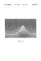
- FIG. 11is a representative graph depicting the veil height remaining in comparison to a chlorine flow rate for the chemical etching process.
- FIG. 12is a graph showing ion energy and ion density compared to RF frequency at which the power supply is provided.
- FIG. 13is a top plan view of a wafer processing apparatus.
- the density of the featurescan be measured by the pitch, where the pitch is defined as sum of the width of the feature and the width of the space between features.
- high density featureshave a pitch which is about and less than 2.0 microns and preferably about and less than 0.5 microns.
- high dielectric emerging filmssuch as lead zirconium titanate (PZT), barium strontium titanate (BST), and bismuth strontium tantalate (Y-1), which dielectric films have dielectric constants in the above 200 range, and typically between 200 and 1,400.
- Such high density, emerging semiconductor structuresemploy material such as platinum (Pt), iridium (Ir), iridium dioxide (lrO 2 ), lead zirconium titanate (PZT), ruthenium (Ru), ruthenium dioxide (RuO 2 ), barium strontium titanate (BST), bismuth strontium tantalate (Y-1), and other emerging films.
- the electrodescan be comprised of, for example, platinum with PZT (having a dielectric constant of about 1,400) or BST or Y-1 deposited therebetween in order to establish the high capacitive value required.
- PZTplatinum with PZT (having a dielectric constant of about 1,400) or BST or Y-1 deposited therebetween in order to establish the high capacitive value required.
- FIGS. 1, 2 and 3micrographs and a schematic of a feature of a semiconductor wafer demonstrating vertical sidewalls with sidewall veils or fences extending upwardly therefrom are depicted.
- These veils 20(FIG. 3) are caused by an ion milling process where sputtering dominates the etching process. Materials sputter from the areas unprotected by the photoresist 22 deposit as said veils 20. As can be seen in FIG. 3, these veils 20 tend to coat the photoresist material 22. When the photoresist material is stripped away, the veils remain as shown in FIG. 2.
- These veilsare comprised of platinum from the platinum layer 24 which as shown in FIG.
- These veilsare redeposits of sputtered platinum and can include other materials such as silicon dioxide, carbon, halogens, and other materials involved in the etching process. These veils can also include materials from other films and layers which are contained in the semiconductor wafer, such as by way of example only, Ir, IrO 2 , PZT, Ru, RuO 2 , BST, and Y-1. It is to be understood that veils caused by ion milling are more prevalent for small pitch patterns, where the pitch is less than 0.5 microns, and thus the above process is most beneficial for the emerging high density DRAM and FRAM devices. The advantage of this operation is the fact that the sidewalls produced are vertical in the 70° to 85° range and higher.
- FIGS. 4 and 5depict the profile of a semiconductor feature produced through a chemical etch process.
- the sidewall 28 of the platinum feature 30has a poor profile, not suitable for dense patterns required for the above referenced advanced semiconductor devices.
- Chemical etchinggiving a sidewall profile of 40° to 50°.
- the photoresist material 32is positioned atop the platinum layer 30, which layer has not been stripped away.
- the present inventionprovides for a continuous etching operation using the benefits of both physical etching (ion milling) and chemical etching in order to produce a semiconductor feature having a profile such as shown in FIG. 10.
- the present inventionincludes an etching apparatus (tri-electrode reactor) 34 as seen in FIG. 6.
- the etching apparatus 34includes a housing 36 and an etching chamber 38.
- a wafer 40is positioned on a bottom electrode 42.
- the chamber 38further includes side peripheral electrode 44 and an upper electrode 46.
- the side peripheral electrode 44can be grounded or allowed to establish a floating potential as a result of the plasma developed in the chamber 38.
- the upper electrode 46is generally grounded. In typical operation, both the side peripheral electrode 44 and the upper electrode 46 are grounded as shown in FIG. 6.
- first power supply 48 and second power supply 50are connected to the bottom electrode 42 through a appropriate circuitry 52 which includes matching networks and a combiner. Further a controller 54 controls the sequencing of the first and second AC power supplies 48, 50.
- the first power supplyoperated in the kilohertz range and is optimally provided at about 450 KHz, and typically in the range of less than 500 KHz.
- the second power supplyoperates in the megahertz range, and typically operates at about 13.56 MHZ, although other frequencies above about 1 MHZ and also multiples of 13.56 MHZ can be used with the present invention.
- ion energyincreases towards the kilohertz range while ion density increases towards the megahertz range. This characteristic is important in the operation of the present invention as described below.
- the present inventionprovides for a continuum of etching starting from predominantly physical etching (ion milling) and continuing to predominantly chemical etching.
- Such a procedureis quite naturally counter-intuitive as the first portion of the process requires physical etching, which physical etching has historically resulted in sidewall veils as shown in FIG. 3.
- the platinum layer 70has substantially vertical sidewalls, and the platinum layer 70 and the photoresist layer 72 has substantially no veils associated therewith.
- the semiconductor waferis rinsed prior to a photoresist stripping operation so that water soluble compounds such as water soluble chlorides can be washed away prior to the photoresist stripping or ash operation.
- a post strip solvent rinse operationis performed.
- ion millingwould be accomplished using argon and chemical etching would be accomplished using chlorine.
- argonwould be supplied to the chamber 38 (FIG. 6) at about approximately 10 SCCM (standard cubic centimeter per minute) to about 50 SCCM and preferably at about 20 SCCM
- the chlorinewould be supplied to the chamber at from about 2 SCCM to about 50 SCCM and preferably in the range of about 5 SCCM to about 10 SCCM.
- the pressure in the chamber during physical etchwould be maintained at approximately 2 to 10 millitorr and preferably at about 5 millitorr with the temperature at approximately 80° C.
- the first power supply 48would be operated at about 450 KHz in the power range of about 50 watts to about 200 watts.
- the second power supply 50would be operated at about 13.56 MHZ in the power range of about 500 watts to about 1100 watts.
- the physical etching operationwould run with a time period of about two-thirds to 100% of end point.
- the optical end point for a platinum structure where the platinum is 1000 angstroms thickwould be approximately 70 seconds for a wafer in the 6" to 8" range.
- Optical end point for such a structure where the platinum is 2000 angstroms thickwould be approximately 150 seconds for a wafer in the 6" to 8" range.
- end pointWhen end point is used as a time measure, a trial physical etch process is run until end point is reached. Thereafter, production runs are made based on a fraction of the end point time determined in the trial run. Alternatively, the timing for the physical etch operation can be obtained without determining end point. For example, the time period required to etch through a film can be determined and then a fraction of that time period, from by way of example only, about two-third to about one hundred percent of that time period, can be used for the physical etch step.
- the processshifts to predominantly chemical etching.
- the argonis preferably maintained at about 20 SCCM and the chlorine flow rates increased preferably to about 15 SCCM.
- the argon gascan have a flow rate of about zero SCCM to about 50 SCCM and the chlorine gas can have a flow rate of about 5 SCCM to about 100 SCCM.
- FIG. 11shows a graph comparing final veil height in angstroms to chlorine flow rates in SCCMs. As the flow rate for the chlorine increases, the veil height decreases and as can be seen with the flow rate at or above about 10 SCCM, the veil is substantially attacked and reduced in size.
- the line identified by 60is for veils which are facing an open area.
- the line 62is for veils with the features spaced at approximately 0.8 microns.
- Line 64represents veils with features spaced at approximately 0.3 microns.
- the pressureis reduced to approximately 2 millitorr to about 10 millitorr and preferably about 2 millitorr.
- the first power supply 48 in the kilohertz rangeis preferably turned off in order to significantly reduce the ion milling effect.
- the first power supplycan operate in the range of about 0 watts to about 50 watts. As seen in FIG. 12, it is the kilohertz range power supply which drives ion milling operation by increasing the ion energy.
- the second power supply 30is maintained at about 13.56 MHZ, with a power of about 500 watts to about 1100 watts.
- the chemical etch processis operated for a platinum thickness of both 1000 angstroms and 2000 angstroms for about 45 seconds to about 120 seconds in order to substantially remove the veils created through the ion milling process.
- chemistriesincluding (1) argon and chlorine, (2) argon, chlorine and hydrogen bromide (HBr), or (3) argon, chlorine and carbonyl gases, (4) any of the above chemistries with oxygen (O 2 ), (5) SF 6 by itself or with any of the above chemistries, (6) NF 3 by itself or with any of the above chemistries, and (7) a fluorocarbon (CxFy) by itself or with other chemistries, are preferred.
- chemistriescan include combinations such as (1) argon and CF 4 , (2) argon, CF 4 , and chlorine, (3) argon, CHF 3 , and chlorine, (4) any of the above combined with hydrogen bromide (HBr), (5) SF 6 by itself or with any of the above chemistries, (6) NF 3 by itself or with any of the above chemistries, (7) a fluorocarbon (CxFy), by itself or with other chemistries, and (8) argon and chlorine gases.
- HBrhydrogen bromide
- the rinse-strip-rinse operationcan be carried out by way of example by the apparatus as shown in FIG. 13.
- the system of FIG. 13includes a vacuum load lock chamber 116, an alignment module 118, two etch modules 120 and 122, and a strip module 124, all of which are connected to a central vacuum chamber 126 through a closable opening and are operated by a computer process control system (not shown).
- Load lock chamber 116houses an internal cassette elevator for holding a wafer cassette (entry cassette).
- Vacuum chamber 126has a robotic wafer handling system 138 for transferring wafers from one chamber or module to another.
- Strip module 124is connected to an atmospheric robotic wafer handling system 132 through a closable opening 127, which in turn is connected to rinse module 125 and atmospheric cassette module 134 (exit cassette).
- An example of a typical rinse module usedis the Semitool Equinox rinse system.
- Atmospheric robotic wafer handling system 132services the atmospheric cassette module 134 which holds wafers after the completion of processing.
- the second robotic wafer handling system 132transfers wafers between strip module 124 and rinse module 125.
- rinse module 125 and robotic handling system 132are designed to maintain the degree of wafer alignment required by strip module 124 for stripping.
- the operation of the present inventionis automated and programmable through a computing system.
- the waferIn operation, after being etched in one of the etching modules 120, 122, the wafer is transported through the strip module 124 to the rinse module 125 by the robotic arm 132 where the first rinse occurs. After this rinse, the robotic arm 132 transfers the wafer back to the strip module 124 where photoresist stripping occurs. After stripping, the wafer is then transported by the robotic arm 32 back to the rinse module 25 for final rinsing.
- the present inventioncan also be used with hard masks (oxides and the like) as well as with composite structures with photoresist.
- the inventionadditionally can be used with a wide range of films in addition to the emerging films specified herein.
- reactors other than that specified abovecan be used with the method.
- the present inventioncan be used with inductively coupled plasma source reactors (ICP).
- ICPinductively coupled plasma source reactors
- Inductively coupled plasma sourcescan include by way of example only helicon reactors and helical reactors.
- the above tri-electrode reactoris a capacitively coupled reactor.
- the present methodcan be used in a reactor that is both inductively coupled and capacitively coupled.
- Other reactorssuch as ECRs, electron cyclotron resonance reactors can be used with the present invention.
- the present inventive apparatus and methodprovides an etching operation including first a physical etching step and then a second chemical etching step in order to accomplish the desired vertical profiles for density patterns on semiconductor wafers required by the emerging DRAMs and FRAMs.
- This inventive apparatus and methodallows the vertical walls to be established and then the veils to be removed.
- the apparatus and methodare capable of handling the new emerging films required for the newest high density semiconductor products.
Landscapes
- Engineering & Computer Science (AREA)
- Physics & Mathematics (AREA)
- Plasma & Fusion (AREA)
- Condensed Matter Physics & Semiconductors (AREA)
- Chemical & Material Sciences (AREA)
- General Physics & Mathematics (AREA)
- Manufacturing & Machinery (AREA)
- Computer Hardware Design (AREA)
- Microelectronics & Electronic Packaging (AREA)
- Power Engineering (AREA)
- Analytical Chemistry (AREA)
- Chemical Kinetics & Catalysis (AREA)
- General Chemical & Material Sciences (AREA)
- Drying Of Semiconductors (AREA)
Abstract
Description
Claims (44)
Priority Applications (7)
| Application Number | Priority Date | Filing Date | Title |
|---|---|---|---|
| US08/742,861US6127277A (en) | 1996-07-03 | 1996-11-01 | Method and apparatus for etching a semiconductor wafer with features having vertical sidewalls |
| PCT/US1997/001002WO1998000859A1 (en) | 1996-07-03 | 1997-01-23 | Method and apparatus for etching a semiconductor wafer |
| CA002259972ACA2259972A1 (en) | 1996-07-03 | 1997-01-23 | Method and apparatus for etching a semiconductor wafer |
| EP97903905AEP0925605A4 (en) | 1996-07-03 | 1997-01-23 | METHOD AND APPARATUS FOR ATTACKING SEMICONDUCTOR WAFERS |
| JP10504081AJP2000514600A (en) | 1996-07-03 | 1997-01-23 | Method and apparatus for etching a semiconductor wafer |
| CNB97197232XACN1148789C (en) | 1996-07-03 | 1997-01-23 | Method and apparatus for etching a semiconductor wafer |
| US09/517,387US6492280B1 (en) | 1996-07-03 | 2000-03-02 | Method and apparatus for etching a semiconductor wafer with features having vertical sidewalls |
Applications Claiming Priority (3)
| Application Number | Priority Date | Filing Date | Title |
|---|---|---|---|
| US08/675,559US6500314B1 (en) | 1996-07-03 | 1996-07-03 | Plasma etch reactor and method |
| US08/678,093US5837217A (en) | 1995-07-21 | 1996-07-11 | Process for the preparation of hydrogen rich gas |
| US08/742,861US6127277A (en) | 1996-07-03 | 1996-11-01 | Method and apparatus for etching a semiconductor wafer with features having vertical sidewalls |
Related Parent Applications (2)
| Application Number | Title | Priority Date | Filing Date |
|---|---|---|---|
| US08/675,559Continuation-In-PartUS6500314B1 (en) | 1996-07-03 | 1996-07-03 | Plasma etch reactor and method |
| US08/678,093Continuation-In-PartUS5837217A (en) | 1995-07-21 | 1996-07-11 | Process for the preparation of hydrogen rich gas |
Related Child Applications (1)
| Application Number | Title | Priority Date | Filing Date |
|---|---|---|---|
| US09/517,387ContinuationUS6492280B1 (en) | 1996-07-03 | 2000-03-02 | Method and apparatus for etching a semiconductor wafer with features having vertical sidewalls |
Publications (1)
| Publication Number | Publication Date |
|---|---|
| US6127277Atrue US6127277A (en) | 2000-10-03 |
Family
ID=27101367
Family Applications (1)
| Application Number | Title | Priority Date | Filing Date |
|---|---|---|---|
| US08/742,861Expired - LifetimeUS6127277A (en) | 1996-07-03 | 1996-11-01 | Method and apparatus for etching a semiconductor wafer with features having vertical sidewalls |
Country Status (1)
| Country | Link |
|---|---|
| US (1) | US6127277A (en) |
Cited By (15)
| Publication number | Priority date | Publication date | Assignee | Title |
|---|---|---|---|---|
| US6326308B1 (en)* | 1999-07-30 | 2001-12-04 | Oki Electric Industry, Co., Ltd. | Method for manufacturing semiconductor storage element |
| US6451665B1 (en)* | 1998-12-11 | 2002-09-17 | Hitachi, Ltd. | Method of manufacturing a semiconductor integrated circuit |
| US20020158047A1 (en)* | 2001-04-27 | 2002-10-31 | Yiqiong Wang | Formation of an optical component having smooth sidewalls |
| US20020158046A1 (en)* | 2001-04-27 | 2002-10-31 | Chi Wu | Formation of an optical component |
| US6492280B1 (en)* | 1996-07-03 | 2002-12-10 | Tegal Corporation | Method and apparatus for etching a semiconductor wafer with features having vertical sidewalls |
| US6673668B2 (en) | 2001-06-12 | 2004-01-06 | Hynix Semiconductor, Inc. | Method of forming capacitor of a semiconductor memory device |
| US6677255B1 (en) | 2002-08-29 | 2004-01-13 | Macroniox International Co., Ltd. | Method for removing fences without reduction of ONO film thickness |
| US6689623B2 (en) | 2001-09-12 | 2004-02-10 | Hynix Semiconductor, Inc. | Method for forming a capacitor |
| US6790782B1 (en)* | 2001-12-28 | 2004-09-14 | Advanced Micro Devices, Inc. | Process for fabrication of a transistor gate including high-K gate dielectric with in-situ resist trim, gate etch, and high-K dielectric removal |
| US20050022839A1 (en)* | 1999-10-20 | 2005-02-03 | Savas Stephen E. | Systems and methods for photoresist strip and residue treatment in integrated circuit manufacturing |
| US6858535B2 (en)* | 1998-09-03 | 2005-02-22 | Micron Technology, Inc. | Methods for patterning metal layers for use with forming semiconductor devices |
| US7005247B1 (en) | 2002-09-06 | 2006-02-28 | Kotusa, Inc. | Controlled selectivity etch for use with optical component fabrication |
| US20070186953A1 (en)* | 2004-07-12 | 2007-08-16 | Savas Stephen E | Systems and Methods for Photoresist Strip and Residue Treatment in Integrated Circuit Manufacturing |
| US20150243478A1 (en)* | 2012-10-05 | 2015-08-27 | Fei Company | High Aspect Ratio Structure Analysis |
| US20230082246A1 (en)* | 2021-09-16 | 2023-03-16 | Kioxia Corporation | Substrate processing apparatus and method for manufacturing semiconductor device |
Citations (20)
| Publication number | Priority date | Publication date | Assignee | Title |
|---|---|---|---|---|
| US2468174A (en)* | 1943-05-06 | 1949-04-26 | Koppers Co Inc | Apparatus for electriclaly transforming materials |
| US3458817A (en)* | 1967-02-13 | 1969-07-29 | Westinghouse Electric Corp | Microwave high power short pulse shaper |
| JPS52127168A (en)* | 1976-04-19 | 1977-10-25 | Fujitsu Ltd | Etching unit |
| US4233109A (en)* | 1976-01-16 | 1980-11-11 | Zaidan Hojin Handotai Kenkyu Shinkokai | Dry etching method |
| EP0026604A1 (en)* | 1979-09-20 | 1981-04-08 | Fujitsu Limited | A method of vapour phase growth and apparatus therefor |
| US4263088A (en)* | 1979-06-25 | 1981-04-21 | Motorola, Inc. | Method for process control of a plasma reaction |
| US4349409A (en)* | 1980-05-12 | 1982-09-14 | Fujitsu Limited | Method and apparatus for plasma etching |
| US4352725A (en)* | 1979-12-15 | 1982-10-05 | Anelva Corporation | Dry etching device comprising an electrode for controlling etch rate |
| US4399016A (en)* | 1981-03-12 | 1983-08-16 | Anelva Corporation | Plasma device comprising an intermediate electrode out of contact with a high frequency electrode to induce electrostatic attraction |
| JPS5916334A (en)* | 1982-07-19 | 1984-01-27 | Matsushita Electronics Corp | Dry etching method |
| US4464223A (en)* | 1983-10-03 | 1984-08-07 | Tegal Corp. | Plasma reactor apparatus and method |
| US4579618A (en)* | 1984-01-06 | 1986-04-01 | Tegal Corporation | Plasma reactor apparatus |
| US4585516A (en)* | 1985-03-04 | 1986-04-29 | Tegal Corporation | Variable duty cycle, multiple frequency, plasma reactor |
| US4889588A (en)* | 1989-05-01 | 1989-12-26 | Tegal Corporation | Plasma etch isotropy control |
| US4902377A (en)* | 1989-05-23 | 1990-02-20 | Motorola, Inc. | Sloped contact etch process |
| JPH03129821A (en)* | 1989-10-16 | 1991-06-03 | Seiko Epson Corp | Manufacture of semiconductor device |
| US5181132A (en)* | 1990-05-31 | 1993-01-19 | Canon Kabushiki Kaisha | Liquid crystal device and method for producing the same with metal spacer in hole of thin film device's insulator |
| US5492855A (en)* | 1993-12-28 | 1996-02-20 | Matsushita Electronics Corporation | Method of dry etching platinum using sulfur containing gas |
| US5498768A (en)* | 1988-07-27 | 1996-03-12 | Hitachi, Ltd. | Process for forming multilayer wiring |
| US5565036A (en)* | 1994-01-19 | 1996-10-15 | Tel America, Inc. | Apparatus and method for igniting plasma in a process module |
- 1996
- 1996-11-01USUS08/742,861patent/US6127277A/ennot_activeExpired - Lifetime
Patent Citations (21)
| Publication number | Priority date | Publication date | Assignee | Title |
|---|---|---|---|---|
| US2468174A (en)* | 1943-05-06 | 1949-04-26 | Koppers Co Inc | Apparatus for electriclaly transforming materials |
| US3458817A (en)* | 1967-02-13 | 1969-07-29 | Westinghouse Electric Corp | Microwave high power short pulse shaper |
| US4233109A (en)* | 1976-01-16 | 1980-11-11 | Zaidan Hojin Handotai Kenkyu Shinkokai | Dry etching method |
| JPS52127168A (en)* | 1976-04-19 | 1977-10-25 | Fujitsu Ltd | Etching unit |
| US4263088A (en)* | 1979-06-25 | 1981-04-21 | Motorola, Inc. | Method for process control of a plasma reaction |
| EP0026604A1 (en)* | 1979-09-20 | 1981-04-08 | Fujitsu Limited | A method of vapour phase growth and apparatus therefor |
| US4352725A (en)* | 1979-12-15 | 1982-10-05 | Anelva Corporation | Dry etching device comprising an electrode for controlling etch rate |
| US4349409A (en)* | 1980-05-12 | 1982-09-14 | Fujitsu Limited | Method and apparatus for plasma etching |
| US4399016A (en)* | 1981-03-12 | 1983-08-16 | Anelva Corporation | Plasma device comprising an intermediate electrode out of contact with a high frequency electrode to induce electrostatic attraction |
| JPS5916334A (en)* | 1982-07-19 | 1984-01-27 | Matsushita Electronics Corp | Dry etching method |
| US4464223A (en)* | 1983-10-03 | 1984-08-07 | Tegal Corp. | Plasma reactor apparatus and method |
| US4464223B1 (en)* | 1983-10-03 | 1991-04-09 | Tegal Corp | |
| US4579618A (en)* | 1984-01-06 | 1986-04-01 | Tegal Corporation | Plasma reactor apparatus |
| US4585516A (en)* | 1985-03-04 | 1986-04-29 | Tegal Corporation | Variable duty cycle, multiple frequency, plasma reactor |
| US5498768A (en)* | 1988-07-27 | 1996-03-12 | Hitachi, Ltd. | Process for forming multilayer wiring |
| US4889588A (en)* | 1989-05-01 | 1989-12-26 | Tegal Corporation | Plasma etch isotropy control |
| US4902377A (en)* | 1989-05-23 | 1990-02-20 | Motorola, Inc. | Sloped contact etch process |
| JPH03129821A (en)* | 1989-10-16 | 1991-06-03 | Seiko Epson Corp | Manufacture of semiconductor device |
| US5181132A (en)* | 1990-05-31 | 1993-01-19 | Canon Kabushiki Kaisha | Liquid crystal device and method for producing the same with metal spacer in hole of thin film device's insulator |
| US5492855A (en)* | 1993-12-28 | 1996-02-20 | Matsushita Electronics Corporation | Method of dry etching platinum using sulfur containing gas |
| US5565036A (en)* | 1994-01-19 | 1996-10-15 | Tel America, Inc. | Apparatus and method for igniting plasma in a process module |
Non-Patent Citations (12)
| Title |
|---|
| A. Yuuki, et al., Novel stacked capacitor technology for 1 Gbit drams with CVD (Ba,Sr)Ti) 3 thin films on a thick storage node of Ru, IEDM Tech. Digest, pp. 115 118, 1995.* |
| A. Yuuki, et al., Novel stacked capacitor technology for 1 Gbit drams with CVD-(Ba,Sr)Ti) 3 thin films on a thick storage node of Ru, IEDM Tech. Digest, pp. 115-118, 1995. |
| B.N. Chapman, Triode Systems for Plasma Etching, IBM Technical Disclosure Bulletin, vol. 21, No. 12, May 1979, IBM Corp. 1979; pp. 5006 5007.* |
| B.N. Chapman, Triode Systems for Plasma Etching, IBM Technical Disclosure Bulletin, vol. 21, No. 12, May 1979, IBM Corp. 1979; pp. 5006-5007. |
| Brochure: The First Low Pressure High Density Single Wafer Etch Technology Has a New Name . . . HRe , High Density Reflected Electron, Tegal Corporation, 1993.* |
| Brochure: The First Low-Pressure High Density Single-Wafer Etch Technology Has a New Name . . . HRe-, High Density Reflected Electron, Tegal Corporation, 1993. |
| V.J. Minkiewicz and B.N. Chapman, Triode plasma etching, Appl.Phys.Lett.34(3); Feb. 1979, p. 192 193.* |
| V.J. Minkiewicz and B.N. Chapman, Triode plasma etching, Appl.Phys.Lett.34(3); Feb. 1979, p. 192-193. |
| W.J. Yoo, et al., Control of the pattern slope in Ar/C12 /O2 plasmas during etching of Pt, 1995 Dry Process Symposium, The Institute of Electrical Engineers of Japan, pp. 191 194 (1995).* |
| W.J. Yoo, et al., Control of the pattern slope in Ar/C12 /O2 plasmas during etching of Pt, 1995 Dry Process Symposium, The Institute of Electrical Engineers of Japan, pp. 191-194 (1995). |
| Y. Nishioka, et al., Giga bit scale dram cell with new simple Ru/(Ba,Sr)Ti) 3 /Ru stacked Capacitors using x ray lithography, IEDM Tech. Digest, pp. 903 906, 1995.* |
| Y. Nishioka, et al., Giga-bit scale dram cell with new simple Ru/(Ba,Sr)Ti) 3 /Ru stacked Capacitors using x-ray lithography, IEDM Tech. Digest, pp. 903-906, 1995. |
Cited By (21)
| Publication number | Priority date | Publication date | Assignee | Title |
|---|---|---|---|---|
| US6492280B1 (en)* | 1996-07-03 | 2002-12-10 | Tegal Corporation | Method and apparatus for etching a semiconductor wafer with features having vertical sidewalls |
| US6858535B2 (en)* | 1998-09-03 | 2005-02-22 | Micron Technology, Inc. | Methods for patterning metal layers for use with forming semiconductor devices |
| US6451665B1 (en)* | 1998-12-11 | 2002-09-17 | Hitachi, Ltd. | Method of manufacturing a semiconductor integrated circuit |
| US6326308B1 (en)* | 1999-07-30 | 2001-12-04 | Oki Electric Industry, Co., Ltd. | Method for manufacturing semiconductor storage element |
| US20050022839A1 (en)* | 1999-10-20 | 2005-02-03 | Savas Stephen E. | Systems and methods for photoresist strip and residue treatment in integrated circuit manufacturing |
| US20050079717A1 (en)* | 1999-10-20 | 2005-04-14 | Savas Stephen E. | Systems and methods for photoresist strip and residue treatment in integrated circuit manufacturing |
| US20020158047A1 (en)* | 2001-04-27 | 2002-10-31 | Yiqiong Wang | Formation of an optical component having smooth sidewalls |
| US20020158046A1 (en)* | 2001-04-27 | 2002-10-31 | Chi Wu | Formation of an optical component |
| US6673668B2 (en) | 2001-06-12 | 2004-01-06 | Hynix Semiconductor, Inc. | Method of forming capacitor of a semiconductor memory device |
| US20040147088A1 (en)* | 2001-09-12 | 2004-07-29 | Hynix Semiconductor, Inc. | Capacitor |
| US6689623B2 (en) | 2001-09-12 | 2004-02-10 | Hynix Semiconductor, Inc. | Method for forming a capacitor |
| US7042034B2 (en) | 2001-09-12 | 2006-05-09 | Hynix Semiconductor Inc. | Capacitor |
| US6790782B1 (en)* | 2001-12-28 | 2004-09-14 | Advanced Micro Devices, Inc. | Process for fabrication of a transistor gate including high-K gate dielectric with in-situ resist trim, gate etch, and high-K dielectric removal |
| US6677255B1 (en) | 2002-08-29 | 2004-01-13 | Macroniox International Co., Ltd. | Method for removing fences without reduction of ONO film thickness |
| US7005247B1 (en) | 2002-09-06 | 2006-02-28 | Kotusa, Inc. | Controlled selectivity etch for use with optical component fabrication |
| US20070186953A1 (en)* | 2004-07-12 | 2007-08-16 | Savas Stephen E | Systems and Methods for Photoresist Strip and Residue Treatment in Integrated Circuit Manufacturing |
| US20070193602A1 (en)* | 2004-07-12 | 2007-08-23 | Savas Stephen E | Systems and Methods for Photoresist Strip and Residue Treatment in Integrated Circuit Manufacturing |
| US20150243478A1 (en)* | 2012-10-05 | 2015-08-27 | Fei Company | High Aspect Ratio Structure Analysis |
| US9741536B2 (en)* | 2012-10-05 | 2017-08-22 | Fei Company | High aspect ratio structure analysis |
| TWI628702B (en)* | 2012-10-05 | 2018-07-01 | Fei公司 | High aspect ratio structure analysis |
| US20230082246A1 (en)* | 2021-09-16 | 2023-03-16 | Kioxia Corporation | Substrate processing apparatus and method for manufacturing semiconductor device |
Similar Documents
| Publication | Publication Date | Title |
|---|---|---|
| US6492280B1 (en) | Method and apparatus for etching a semiconductor wafer with features having vertical sidewalls | |
| US6037264A (en) | Method for removing redeposited veils from etched platinum | |
| US6323132B1 (en) | Etching methods for anisotropic platinum profile | |
| US6777342B2 (en) | Method of plasma etching platinum | |
| US6127277A (en) | Method and apparatus for etching a semiconductor wafer with features having vertical sidewalls | |
| US6919168B2 (en) | Masking methods and etching sequences for patterning electrodes of high density RAM capacitors | |
| KR19980080224A (en) | Method for removing redeposited bales from etched platinum | |
| US6368517B1 (en) | Method for preventing corrosion of a dielectric material | |
| US6265318B1 (en) | Iridium etchant methods for anisotropic profile | |
| US6943039B2 (en) | Method of etching ferroelectric layers | |
| JP2003282844A (en) | Plasma etching of Ir and PZT using hard mask and chemistry of Cl2 / N2 / O2 and Cl2 / CHF3 / O2 | |
| US6454956B1 (en) | Structuring method | |
| US6315913B1 (en) | Structuring method | |
| KR100537231B1 (en) | Semiconductor Wafer Etching Method and Apparatus | |
| KR20010088057A (en) | Dry etching method of iridium electrode | |
| JP2003529914A (en) | Improved masking method and etching arrangement for patterning electrodes of high density RAM capacitors | |
| KR20020009696A (en) | Method for forming pattern capable of removing polymer generated on sidewall of photoresist pattern and method for forming ferroelectric capacitor using the same | |
| JP2001339053A (en) | Method for manufacturing semiconductor device |
Legal Events
| Date | Code | Title | Description |
|---|---|---|---|
| AS | Assignment | Owner name:TEGAL CORPORATION, CALIFORNIA Free format text:ASSIGNMENT OF ASSIGNORS INTEREST;ASSIGNORS:DEORNELLAS, STEPHEN P.;COFER, ALFERD;RAJORA, PARITOSH;REEL/FRAME:008300/0772 Effective date:19961101 | |
| AS | Assignment | Owner name:IMPERIAL BANK, CALIFORNIA Free format text:SECURITY AGREEMENT;ASSIGNOR:TEGAL CORPORATION;REEL/FRAME:010018/0169 Effective date:19980815 | |
| STCF | Information on status: patent grant | Free format text:PATENTED CASE | |
| AS | Assignment | Owner name:SILICON VALLEY BANK, CALIFORNIA Free format text:SECURITY AGREEMENT;ASSIGNOR:TEGAL CORPORATION;REEL/FRAME:013506/0749 Effective date:20020626 | |
| AS | Assignment | Owner name:HIRSCHMAN, ORIN, NEW YORK Free format text:SECURITY INTEREST;ASSIGNOR:TEGAL CORPORATION;REEL/FRAME:014242/0813 Effective date:20030630 | |
| FPAY | Fee payment | Year of fee payment:4 | |
| FPAY | Fee payment | Year of fee payment:8 | |
| AS | Assignment | Owner name:OEG-TEG, LLC,ARIZONA Free format text:ASSIGNMENT OF ASSIGNORS INTEREST;ASSIGNOR:TEGAL CORPORATION;REEL/FRAME:024547/0285 Effective date:20100319 Owner name:OEM GROUP INC.,ARIZONA Free format text:ASSIGNMENT OF ASSIGNORS INTEREST;ASSIGNOR:OEG-TEG, LLC;REEL/FRAME:024547/0404 Effective date:20100319 | |
| AS | Assignment | Owner name:COMERICA BANK, A TEXAS BANKING ASSOCIATION, MICHIG Free format text:SECURITY AGREEMENT;ASSIGNOR:OEM GROUP, INC.;REEL/FRAME:025105/0799 Effective date:20101007 | |
| AS | Assignment | Owner name:THL CORPORATE FINANCE, INC., MASSACHUSETTS Free format text:SECURITY AGREEMENT;ASSIGNOR:OEM GROUP, INC.;REEL/FRAME:025137/0859 Effective date:20101007 | |
| FPAY | Fee payment | Year of fee payment:12 | |
| AS | Assignment | Owner name:OEM GROUP, LLC, ARIZONA Free format text:CHANGE OF NAME;ASSIGNOR:OEM GROUP, INC.;REEL/FRAME:038083/0231 Effective date:20160309 | |
| AS | Assignment | Owner name:THL CORPORATE FINANCE, INC., AS COLLATERAL AGENT, Free format text:SECURITY INTEREST;ASSIGNOR:OEM GROUP, LLC;REEL/FRAME:038355/0078 Effective date:20160316 |