US6127249A - Metal silicidation methods and methods for using same - Google Patents
Metal silicidation methods and methods for using sameDownload PDFInfo
- Publication number
- US6127249A US6127249AUS08/803,528US80352897AUS6127249AUS 6127249 AUS6127249 AUS 6127249AUS 80352897 AUS80352897 AUS 80352897AUS 6127249 AUS6127249 AUS 6127249A
- Authority
- US
- United States
- Prior art keywords
- cobalt
- layer
- titanium
- nitridated
- silicon
- Prior art date
- Legal status (The legal status is an assumption and is not a legal conclusion. Google has not performed a legal analysis and makes no representation as to the accuracy of the status listed.)
- Expired - Lifetime
Links
Images


Classifications
- H—ELECTRICITY
- H01—ELECTRIC ELEMENTS
- H01L—SEMICONDUCTOR DEVICES NOT COVERED BY CLASS H10
- H01L21/00—Processes or apparatus adapted for the manufacture or treatment of semiconductor or solid state devices or of parts thereof
- H01L21/02—Manufacture or treatment of semiconductor devices or of parts thereof
- H01L21/04—Manufacture or treatment of semiconductor devices or of parts thereof the devices having potential barriers, e.g. a PN junction, depletion layer or carrier concentration layer
- H01L21/18—Manufacture or treatment of semiconductor devices or of parts thereof the devices having potential barriers, e.g. a PN junction, depletion layer or carrier concentration layer the devices having semiconductor bodies comprising elements of Group IV of the Periodic Table or AIIIBV compounds with or without impurities, e.g. doping materials
- H01L21/28—Manufacture of electrodes on semiconductor bodies using processes or apparatus not provided for in groups H01L21/20 - H01L21/268
- H01L21/28008—Making conductor-insulator-semiconductor electrodes
- H01L21/28017—Making conductor-insulator-semiconductor electrodes the insulator being formed after the semiconductor body, the semiconductor being silicon
- H01L21/28026—Making conductor-insulator-semiconductor electrodes the insulator being formed after the semiconductor body, the semiconductor being silicon characterised by the conductor
- H01L21/28035—Making conductor-insulator-semiconductor electrodes the insulator being formed after the semiconductor body, the semiconductor being silicon characterised by the conductor the final conductor layer next to the insulator being silicon, e.g. polysilicon, with or without impurities
- H01L21/28044—Making conductor-insulator-semiconductor electrodes the insulator being formed after the semiconductor body, the semiconductor being silicon characterised by the conductor the final conductor layer next to the insulator being silicon, e.g. polysilicon, with or without impurities the conductor comprising at least another non-silicon conductive layer
- H01L21/28052—Making conductor-insulator-semiconductor electrodes the insulator being formed after the semiconductor body, the semiconductor being silicon characterised by the conductor the final conductor layer next to the insulator being silicon, e.g. polysilicon, with or without impurities the conductor comprising at least another non-silicon conductive layer the conductor comprising a silicide layer formed by the silicidation reaction of silicon with a metal layer
- H—ELECTRICITY
- H01—ELECTRIC ELEMENTS
- H01L—SEMICONDUCTOR DEVICES NOT COVERED BY CLASS H10
- H01L21/00—Processes or apparatus adapted for the manufacture or treatment of semiconductor or solid state devices or of parts thereof
- H01L21/02—Manufacture or treatment of semiconductor devices or of parts thereof
- H01L21/04—Manufacture or treatment of semiconductor devices or of parts thereof the devices having potential barriers, e.g. a PN junction, depletion layer or carrier concentration layer
- H01L21/18—Manufacture or treatment of semiconductor devices or of parts thereof the devices having potential barriers, e.g. a PN junction, depletion layer or carrier concentration layer the devices having semiconductor bodies comprising elements of Group IV of the Periodic Table or AIIIBV compounds with or without impurities, e.g. doping materials
- H01L21/28—Manufacture of electrodes on semiconductor bodies using processes or apparatus not provided for in groups H01L21/20 - H01L21/268
- H01L21/283—Deposition of conductive or insulating materials for electrodes conducting electric current
- H01L21/285—Deposition of conductive or insulating materials for electrodes conducting electric current from a gas or vapour, e.g. condensation
- H01L21/28506—Deposition of conductive or insulating materials for electrodes conducting electric current from a gas or vapour, e.g. condensation of conductive layers
- H01L21/28512—Deposition of conductive or insulating materials for electrodes conducting electric current from a gas or vapour, e.g. condensation of conductive layers on semiconductor bodies comprising elements of Group IV of the Periodic Table
- H01L21/28518—Deposition of conductive or insulating materials for electrodes conducting electric current from a gas or vapour, e.g. condensation of conductive layers on semiconductor bodies comprising elements of Group IV of the Periodic Table the conductive layers comprising silicides
- H—ELECTRICITY
- H01—ELECTRIC ELEMENTS
- H01L—SEMICONDUCTOR DEVICES NOT COVERED BY CLASS H10
- H01L21/00—Processes or apparatus adapted for the manufacture or treatment of semiconductor or solid state devices or of parts thereof
- H01L21/02—Manufacture or treatment of semiconductor devices or of parts thereof
- H01L21/04—Manufacture or treatment of semiconductor devices or of parts thereof the devices having potential barriers, e.g. a PN junction, depletion layer or carrier concentration layer
- H01L21/18—Manufacture or treatment of semiconductor devices or of parts thereof the devices having potential barriers, e.g. a PN junction, depletion layer or carrier concentration layer the devices having semiconductor bodies comprising elements of Group IV of the Periodic Table or AIIIBV compounds with or without impurities, e.g. doping materials
- H01L21/28—Manufacture of electrodes on semiconductor bodies using processes or apparatus not provided for in groups H01L21/20 - H01L21/268
- H01L21/283—Deposition of conductive or insulating materials for electrodes conducting electric current
- H01L21/285—Deposition of conductive or insulating materials for electrodes conducting electric current from a gas or vapour, e.g. condensation
- H01L21/28506—Deposition of conductive or insulating materials for electrodes conducting electric current from a gas or vapour, e.g. condensation of conductive layers
- H01L21/28512—Deposition of conductive or insulating materials for electrodes conducting electric current from a gas or vapour, e.g. condensation of conductive layers on semiconductor bodies comprising elements of Group IV of the Periodic Table
- H01L21/28568—Deposition of conductive or insulating materials for electrodes conducting electric current from a gas or vapour, e.g. condensation of conductive layers on semiconductor bodies comprising elements of Group IV of the Periodic Table the conductive layers comprising transition metals
- Y—GENERAL TAGGING OF NEW TECHNOLOGICAL DEVELOPMENTS; GENERAL TAGGING OF CROSS-SECTIONAL TECHNOLOGIES SPANNING OVER SEVERAL SECTIONS OF THE IPC; TECHNICAL SUBJECTS COVERED BY FORMER USPC CROSS-REFERENCE ART COLLECTIONS [XRACs] AND DIGESTS
- Y10—TECHNICAL SUBJECTS COVERED BY FORMER USPC
- Y10S—TECHNICAL SUBJECTS COVERED BY FORMER USPC CROSS-REFERENCE ART COLLECTIONS [XRACs] AND DIGESTS
- Y10S438/00—Semiconductor device manufacturing: process
- Y10S438/902—Capping layer
Definitions
- the present inventionrelates to the fabrication of semiconductor devices. More particularly, the present invention relates to metal silicidation methods for silicidation using metals, such as, for example, cobalt.
- Various metalization, interconnect, and polycide formation processesare known and used in the fabrication of semiconductor devices.
- SRAMsstatic random access memories
- DRAMsdynamic random access memories
- local interconnectsare used to increase packing density and metal suicides are used for metalization of contact junctions and for forming polycide lines, such as bit lines, word lines, or other local interconnection of device elements being fabricated.
- polycide linessuch as bit lines, word lines, or other local interconnection of device elements being fabricated.
- line widths of semiconductor devicesdecrease, desire for low resistance polycides with low aspect ratios has led to the consideration of various polycide materials other than the conventional tungsten or titanium silicide.
- a desire for low resistivity materials for metalization of such junction contacts as an alternative to titanium silicideare also desired.
- titanium thickness used in a silicidation processmust be reduced, which, in turn, undesirably increases the Kelvin contact resistance.
- titanium silicideis a large grain material.
- Thin titanium silicidehas nonuniform large grain size that contributes to a very rough titanium silicide/silicon interface. As such, it reduces the effective ohmic contact area.
- effective methods for forming such materialssuch as cobalt silicide, need to be developed.
- junction spiking at the cobalt silicide/silicon interface associated with the use of cobalt as the predominant diffusion species in a silicide processtends to form spiking related pittings, i.e., voids in the cobalt silicide formed.
- Such pittings or voidsare detrimental to the performance of devices fabricated with such a cobalt silicidation process as the pittings may penetrate through the shallow junction to cause junction leakage.
- dopants and impuritiescan diffuse out of cobalt silicide easily. As such, diffusion of impurities out of the cobalt towards the gate oxide of a device may occur. For example, diffusion of impurities, such as alkali metals, may occur in the metalization of a bit line contact during a cobalt silicidation anneal. Such diffusion of unwanted impurities into the gate region may also be detrimental to the devices being fabricated.
- silicidation methods using cobaltare known. For example, in one such method, a layer of cobalt is deposited over silicon regions and then an anneal is performed to react the cobalt with the silicon to silicide the silicon regions with the formation of cobalt silicide.
- titanium and then cobaltare deposited on a silicon region and then annealed. During the annealing process, the titanium reacts with the silicon region and then diffuses upward with the cobalt diffusing downward to silicide the silicon regions resulting in the formation of cobalt silicide.
- This methodis known as a titanium/cobalt reversal silicidation process.
- one shortcoming associated with the nitridation of cobalt or nickel films to decrease junction pittings or voidsis that the difficulty of the silicidation process using such nitridated films increases with the increasing percentage of nitrogen incorporated therein. For example, the temperature of the anneal necessary for obtaining the same resistance for the silicidation process when utilizing cobalt or nickel films having increasing nitrogen concentrations, increases as well.
- a method in accordance with the present invention for use in the fabrication of semiconductor devicesincludes forming a layer of nitridated cobalt on a surface of a silicon region and forming a film cap including titanium over the layer of cobalt. A thermal treatment is then performed to form cobalt silicide from the layer of nitridated cobalt and at least a portion of the silicon region.
- the formation of the film capincludes forming a thin cap of titanium or titanium nitride having a thickness less than about 15 nanometers. More preferably, the thickness of the thin cap is in the range of about 3 nanometers to about 5 nanometers.
- the layer of nitridated cobaltis formed in an atmosphere including nitrogen and the nitrogen incorporated in the layer is a percentage volume of about 10% or less.
- the thermal treatmentmay be performed at a temperature less than 900° C. to form the cobalt silicide from the layer of cobalt and at least a portion of the silicon region.
- the methodincludes forming a titanium film over a surface of a silicon region in an atmosphere including at least one of nitrogen and oxygen. A layer of one of cobalt or nickel is formed over the titanium film. A thermal treatment is then performed for reversal and silicidation of the titanium film and the layer of cobalt or nickel to form cobalt silicide or nickel silicide.
- the reversal and silicidation of the titanium film and the layer of cobalt or nickelincludes performing an anneal to form at least a titanium silicide region from the titanium film and at least a portion of the silicon region. Thereafter, an additional anneal is performed to form cobalt silicide or nickel silicide from the layer of cobalt or nickel and at least a portion of the titanium silicide region and the silicon region.
- the atmosphereincludes less than about 3% by volume of nitrogen.
- the atmosphereincludes nitrogen in the range of about 0.1% to about 1% by volume.
- the atmosphereincludes less than about 10% by volume of oxygen.
- the atmosphereincludes oxygen in the range of about 0.01% to about 1% by volume.
- silicidation of a silicon contact areais performed and a polycide line is formed using methods similar to those described above.
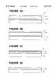
- FIGS. 1A-1Care illustrative diagrams showing the steps of siliciding a silicon region using a titanium film cap and a nitridated cobalt layer in accordance with the present invention.
- FIGS. 2A-2Dare illustrative diagrams showing the steps of siliciding a silicon region using a layer reversal step and incorporation of oxygen into one of the layers reversed in accordance with the present invention.
- FIGS. 3A-3Dare illustrative diagrams showing the steps of siliciding a silicon region using a layer reversal step and incorporation of nitrogen into one of the layers reversed in accordance with the present invention.
- FIGS. 4A-4Dare illustrative diagrams showing the metalization of a junction contact in accordance with the present invention.
- FIGS. 5A-5Dare illustrative diagrams showing the formation of a polycide line in accordance with the present invention.
- FIGS. 6A-6Bare images showing pittings or voids of silicided silicon using cobalt without a titanium film cap.
- FIGS. 7A-7Bare images showing a virtual absence of pittings or voids of silicided silicon using cobalt with a titanium film cap.
- FIGS. 8A-8D, 9A-9D, and 10A-10Dare graphs showing a comparison of sheet resistivity between silicidation processes with use of a titanium film cap versus without the use of a titanium film cap.
- FIG. 11is a diagram showing the concentrations of various materials of a silicided silicon region with the use of a titanium film cap.
- FIGS. 1A-1C, 2A-2D, and 3A-3DVariations of silicidation processes are shown in each of these groups of figures. With the description as provided below, it is readily apparent to one skilled in the art that the various processes described with respect to each group of figures may be utilized alone as a separate process, with process steps from one substituted for process steps of the other, or in various configurations, with process steps of one used as additional process steps or in combination with the process steps of the other.
- the silicidation process using a nitridated cobalt layer and a titanium film capmay utilize a reversal silicidation process as described below.
- a reversal silicidation processwhich provides for efficient incorporation of nitrogen or uses incorporation of oxygen for impurity removal may use a titanium film cap.
- the present inventionis not limited to the particular process steps of each group of figures as a standalone silicidation process, but is limited only as described in the accompanying claims.
- FIGS. 1A-1Cshow process steps of a method to effectively facilitate metal silicidation of a nitridated cobalt film by using a low temperature thin titanium film cap.
- the temperature at which the cobalt silicidation process can be performedis lowered relative to conventional cobalt silicidation processes.
- nitridation during the deposition of a cobalt thin film in combination with a thin titanium film capreduces the likelihood of spiking or the number of pittings or voids in the cobalt silicide film formed during the silicidation process.
- FIGS. 2A-2Dshow process steps of a thin film gettering method to purify the cobalt silicide formed during a silicidation process.
- a stack of cobalt and titaniumis formed over a silicon region, with or without a cap including titanium over the cobalt.
- the titanium deposited on the silicon regionis deposited with a small volume of oxygen in the atmosphere which forms small amounts of titanium oxide in the titanium film.
- Two techniquesare then used to achieve gettering, i.e., removal of impurities, and formation of the cobalt silicide.
- a snow plowing effectpushes light density titanium oxide towards the titanium/cobalt interface during a thermal treatment in which titanium silicide is formed.
- a thermal treatmentis then used to perform a reversal of the titanium silicide and the cobalt to form the cobalt silicide over the silicon region.
- the impuritiesare plowed to the upper portion of the stack, i.e., out of the formed cobalt silicide.
- FIGS. 3A-3Dshow the process steps of efficiently and indirectly incorporating light concentrations of nitrogen into cobalt silicide formed during a silicidation process.
- Such light nitridation of the cobalt silicideimproves leakage current through the reduction of spiking or pittings in the cobalt silicide formed.
- a stack of cobalt and titaniumis formed over a silicon region, with or without a cap including titanium over the cobalt.
- the titanium deposited on the silicon regionis deposited with a small volume of nitrogen in the atmosphere which incorporates small amounts of nitrogen in the preformed titanium film.
- a first thermal treatmentin which titanium silicide is formed, a low concentration of TiN x or SiN x remains in the titanium silicide.
- a thermal treatmentis used to perform a reversal of the titanium silicide and the cobalt to form the cobalt silicide over the silicon region with the TiN x or SiN x remaining in the cobalt silicide.
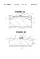
- the silicidation process as shown thereinincludes forming a cobalt layer 12 over a surface of a substrate assembly 10.
- Substrate assemblyrefers to a semiconductor substrate which includes a base layer of silicon material of the device being fabricated or a silicon layer formed on another material, such as, for example, silicon on sapphire.
- Further substrate assemblyrefers to a semiconductor substrate having one or more various layers formed thereon.
- the surface upon which cobalt layer 12 is depositedmay include various surfaces, including but not limited to, a silicon containing surface of a silicon region (i.e., a doped or undoped silicon region for silicidation and metalization thereof), of a polysilicon region (i.e., a doped or undoped polysilicon region such as for formation of a polycide line), or of various other surfaces such as for interconnect between at least two elements of a device structure with a polycide line (i.e., drain to a bit line of a device).
- the cobaltmay be deposited over a polysilicon layer which is formed over a gate oxide and field oxide regions of a device being formed as further described in the illustration provided below.
- the cobalt layer 12may be deposited at various thicknesses depending upon the application of the silicidation process and the desired resistance of the resulting cobalt silicide. For example, in the metalization of a contact junction, the thickness may be in the range of about 50 ⁇ to about 150 ⁇ .
- the cobaltmay be deposited by various methods.
- the cobalt layer 12may be deposited, for example, by sputtering, evaporation, physical or chemical vapor deposition.
- the processmay be performed by using an argon gas as the sputtering gas at a particular flow rate, with the application of an RF power for achieving the desired deposition in a pressurizable sputtering chamber.
- any manner of forming the cobalt layeris contemplated in accordance with the present invention and is in no manner limited to any particular process, i.e., sputtering, for formation thereof.
- the cobalt layer 12is formed with the incorporation of a certain percentage of nitrogen therein.
- the percentage of nitrogen incorporated thereinis preferably 10% or less by volume.
- the incorporation of nitrogen into the cobalt layermay be performed by sputtering cobalt with use of an Argon sputtering gas in a MRC Eclipse PVD system available from MRC (Gilbert, Ariz.), in an atmosphere including nitrogen. With the incorporation of nitrogen into the cobalt layer 12, spiking related pittings or voids are reduced as is shown by the Examples below.
- the difficulty of performing the silicidation processis increased.
- the amount of unreacted cobaltincreases with nitridation even after high temperature anneals.
- a titanium film cap 14is formed over the cobalt layer 12.
- the titanium film cap 14may be formed, for example, by sputtering, evaporation, physical vapor deposition or chemical vapor deposition. Although any thickness of the titanium film cap 14 may be used, preferably, the titanium cap 14 is formed to a thickness less than 15 nanometers, and more preferably, in the range of about 3 nanometers to about 5 nanometers. Further, the titanium film cap is preferably formed at a temperature of less than about 100° C. to improve layer to layer coverage of the titanium film cap 14 over the cobalt layer 12. As an alternative to a thin titanium cap being used, a thin titanium nitride cap may also be utilized.
- the structure as shown in FIG. 1Ais subjected to a silicidation anneal forming the cobalt silicide layer 16 over the silicon containing layer 10 and layer 18 which includes at least one of titanium, nitrogen, titanium oxide, titanium nitride, oxygen, and even unreacted cobalt.
- the annealmay be a rapid thermal process (RTP) anneal in the temperature range of about 500° C. to about 900° C. for about 10 to about 40 seconds. It should be apparent and as described in the Examples below, that the thermal treatment will vary depending upon various factors such as thickness of the cobalt layer, resistivity desired, etc.
- the thermal treatmentmay also be a conventional furnace anneal as opposed to an RTP anneal and further may include various anneal steps, whether furnace or RTP anneal, in temperature and duration.
- the layer 18may be removed.
- the layer 18may be removed using any known stripping method for removing a titanium containing layer, whether dry or wet.
- the stripmay include a mixture of ammonia and hydrogen peroxide, or a mixture of sulfuric acid and hydrogen peroxide.
- layer 18may be removed by a dry etch such as with utilization of a fluorine or chlorine containing plasma, such as CF 4 , SF 6 .
- the resulting layers, including cobalt silicide layer 16 and substrate or substrate assembly 10,are illustrated in FIG. 1C.
- the thin film cap including titanium and the incorporation of nitrogen in the cobalt layerimproves the resistance values of the cobalt silicide formed by the silicidation process as it facilitates the silicidation process, i.e., decreases the amount of unreacted cobalt. These results occur even when the nitrogen incorporated is low.
- the results obtained using the titanium film capare caused by the diffusion of a small amount of titanium into the cobalt film.
- the titanium atomsdiffused into the cobalt or cobalt silicide grain boundaries, particularly when the anneal is being performed and since silicon is the predominant diffusion species in titanium silicidation processes, the silicon is further drawn upward towards the titanium atoms through the cobalt layer 12 to facilitate the silicidation of the cobalt layer 12.
- the following examplesare used to point out the beneficial effects of using a titanium film cap 14 in the silicidation of nitridated cobalt layer 12.
- the formation of a cobalt layer over HF dipped silicon wafers, and the formation of the titanium film cap, if applicable,were performed using a MRC Eclipse PVD system available from MRC, (Gilbert, Ariz.) using an Argon sputtering gas.
- MRC Eclipse PVD systemavailable from MRC, (Gilbert, Ariz.) using an Argon sputtering gas.
- the various different characteristics of the examplewill be noted, i.e, thickness of cobalt deposited, temperatures of the anneals, etc.
- FIGS. 6A-6B and FIGS. 7A-7Bthree wafers, wafer1-3, were run at slightly different parameters and with various characteristics.
- FIGS. 6A and 6Bare Normarsky images of wafer1.
- Wafer1included an HF dipped silicon wafer with an unnitridated layer of cobalt formed thereon at a thickness of about 75 ⁇ .
- a silicidation RTP anneal at about 630° C.was performed for about 20 seconds in a nitrogen atmosphere. No titanium film cap was utilized.
- FIG. 6Ais an image at the center of the wafer1 and FIG. 6B is an image at an edge of the wafer1.
- FIG. 7Ais a Normarsky image of wafer2.
- Wafer2included an HF dipped silicon wafer with a nitridated layer of cobalt formed thereon at a thickness of about 88 ⁇ . The percentage of nitrogen incorporated into the film was about 5%.
- a titanium film cap of about 5 nanometers at about 100° C.was formed over the cobalt layer.
- a silicidation RTP anneal at about 700° C.was performed for about 15 seconds in a nitrogen atmosphere.
- FIG. 7Ais an image at the center of the wafer2. An image at the edge of the wafer was insignificantly different, containing virtually no pittings or voids.
- FIG. 7Bis a Normarsky image of wafer3.
- Wafer3included an HF dipped silicon wafer with a nitridated layer of cobalt formed thereon at a thickness of about 105 ⁇ . The percentage of nitrogen incorporated into the film was about 10%. A titanium film cap was not utilized. A silicidation RTP anneal at about 700° C. was performed for about 15 seconds in a nitrogen atmosphere.
- FIG. 7Bis an image at the center of the wafer3.
- the imagesgenerally show the reduction of pittings using a film cap including titanium for the silicidation of nitridated cobalt, i.e., nitrogen incorporated at a volume of about 5%, which is further substantiated by the examples that follow.
- FIGS. 8A-8Deight wafers were initially prepared, e.g., Step 0, with substantially equivalent characteristics and parameters.
- the waferswere initially HF dipped silicon wafers with an unnitridated layer of cobalt formed thereon at a temperature of about 100° C. and a thickness of about 75 ⁇ .
- Step 1a silicidation RTP anneal at about 630° C. was performed for about 20 seconds in a nitrogen atmosphere;
- Step 2a silicidation RTP anneal at about 700° C. was performed for about 15 seconds in a nitrogen atmosphere;
- Step 3a silicidation RTP anneal at about 730° C. was performed for about 10 seconds in a nitrogen atmosphere;
- Step 4a silicidation RTP anneal at about 765° C. was performed for about 30 seconds in a nitrogen atmosphere.
- FIGS. 8A and 8Bresistance measurements were taken as described above at the completion of each step.
- FIG. 8Ashows the resistance values in ohms/square and
- FIG. 8Bshows the standard deviation of the resistance measurements from center to edge of wafers measured.
- Step 1a titanium film cap of about 5 nanometers in thickness was deposited at a temperature of about 100° C.;
- Step 2a silicidation RTP anneal at about 700° C. was performed for about 15 seconds in a nitrogen atmosphere;
- Step 3a silicidation RTP anneal at about 850° C. was performed for about 30 seconds in a nitrogen atmosphere.
- FIGS. 8C and 8Dresistance measurements were taken as described above at the completion of each step.
- FIG. 8Cshows the resistance values in ohms/square and
- FIG. 8Dshows the standard deviation of the resistance measurements from center to edge of wafers measured.
- FIGS. 9A-9Deight wafers were initially prepared, e.g., Step 0, with substantially equivalent characteristics and parameters.
- the waferswere initially HF dipped silicon wafers with a nitridated layer of cobalt formed thereon at a temperature of about 100° C. and a thickness of about 88 ⁇ .
- the percentage of nitrogen incorporated into the cobalt filmwas about 5%.
- Step 1a silicidation RTP anneal at about 700° C. was performed for about 15 seconds in a nitrogen atmosphere;
- Step 2a silicidation RTP anneal at about 765° C. was performed for about 30 seconds in a nitrogen atmosphere.
- FIGS. 9A and 9Bresistance measurements were taken as described above at the completion of each step.
- FIG. 9Ashows the resistance values in ohms/square and
- FIG. 9Bshows the standard deviation of the resistance measurements from the center to edge of wafers measured.
- Step 1a titanium film cap of about 5 nanometers in thickness was deposited at a temperature of about 100° C.; Step 2: a silicidation RTP anneal at about 700° C. was performed for about 15 seconds in a nitrogen atmosphere.
- FIGS. 9C and 9Dresistance measurements were taken as described above at the completion of each step.
- FIG. 9Cshows the resistance values in ohms/square and
- FIG. 9Dshows the standard deviation of the resistance measurements from center to edge of wafers measured.
- FIGS. 10A-10Deight wafers were initially prepared, e.g., Step 0, with substantially equivalent characteristics and parameters.
- the waferswere initially HF dipped silicon wafers with a nitridated layer of cobalt formed thereon at a temperature of about 100° C. and a thickness of about 105 ⁇ .
- the percentage of nitrogen incorporated into the cobalt filmwas about 10%.
- Step 1a silicidation RTP anneal at about 700° C. was performed for about 15 seconds in a nitrogen atmosphere;
- Step 2a silicidation RTP anneal at about 765° C. was performed for about 30 seconds in a nitrogen atmosphere;
- Step 3a silicidation RTP anneal at about 850° C. was performed for about 30 seconds in a nitrogen atmosphere;
- Step 4a silicidation RTP anneal at about 880° C. was performed for about 30 seconds in a nitrogen atmosphere.
- FIGS. 10A and 10Bresistance measurements were taken as described above at the completion of each step.
- FIG. 10Ashows the resistance values in ohms/square and
- FIG. 10Bshows the standard deviation of the resistance measurements from center to edge of wafers measured.
- Step 1a titanium film cap of about 5 nanometers in thickness was deposited at a temperature of about 100° C.;
- Step 2a silicidation RTP anneal at about 700° C. was performed for about 15 seconds in a nitrogen atmosphere;
- Step 3a silicidation RTP anneal at about 765° C. was performed for about 30 seconds in a nitrogen atmosphere;
- Step 4a silicidation RTP anneal at about 850° C. was performed for about 30 seconds in a nitrogen atmosphere.
- FIGS. 10C and 10Dresistance measurements were taken as described above at the completion of each step.
- FIG. 10Cshows the resistance values in ohms/square and
- FIG. 10Dshows the standard deviation of the resistance measurements from center to edge of wafers measured.
- FIGS. 8A, 9A, 10Awhich show an increasing percentage of nitrogen in the cobalt film without the use of a titanium cap, the difficulty in performing the silicidation process increases.
- the silicidation that occurs with the use of 10% cobaltis so little that the resistance remains above 180 ohms/square even after an anneal above 850° C.
- the resistancedrops to about 11 ohms/square for a 10% nitridated cobalt layer with a titanium film cap used thereover. This is in direct comparison to the 180 ohms/square for such a nitridated layer as shown in FIG. 10A. Such an improvement is also shown at lower nitridation levels.
- FIGS. 9A and 9Cat 5% nitridation of the cobalt layer sheet resistance is improved from about 48 ohms/square to about 8 ohms/square after the same 700° C. anneal.
- the sheet resistancedrops from about 34 ohms/square to about 9 ohms/square after the same 700° C. anneal with the use of a titanium film cap on an unnitridated layer of cobalt.
- the thermal stability of the cobalt silicideis demonstrated from the above Examples.
- the addition of a thin titanium film capshows such stability.
- the cobalt silicidebecomes unstable for an RTP anneal above 750° C. while the sheet resistance remains virtually unchanged when the cobalt film is capped even after an 850° C. anneal (FIG. 8C).
- the interface between the cobalt silicide region 206 and titanium film region 202is shown by line 200. It is readily apparent that the titanium cap is still in place as shown by the high titanium concentration at a depth from 0 to 200 ⁇ . It is shown from the profile that titanium atoms are distributed in the cobalt silicide and cobalt by diffusion of the titanium therein.
- the silicon contentis shown by line 204, the cobalt content by line 208, and the titanium content by line 210.
- the other linesrepresent the small concentrations of oxygen, carbon, and nitrogen.
- the sheet resistance of the structurewas measured at about 9.5 ohms/square and a standard deviation of about 4%.
- the silicidation processincludes forming a titanium layer 22 and then a cobalt layer 24 over a surface of a substrate assembly 20 (FIG. 2A) which includes by definition a semiconductor substrate.
- a substrate assembly 20FIG. 2A
- the surface upon which cobalt layer 24 is depositedis a titanium surface.
- the titanium surfaceis therefore formed on a surface of a silicon region (i.e., a doped or undoped silicon region for silicidation and metalization thereof), a polysilicon region (i.e., a doped or undoped polysilicon region such as for formation of a polycide line), or various other surfaces such as for interconnect between at least two elements of a device structure such as with a polycide line (i.e., drain to a bit line of a device) and can be considered part of the substrate assembly upon which the cobalt layer 24 is formed.
- a silicon regioni.e., a doped or undoped silicon region for silicidation and metalization thereof
- a polysilicon regioni.e., a doped or undoped polysilicon region such as for formation of a polycide line
- various other surfacessuch as for interconnect between at least two elements of a device structure such as with a polycide line (i.e., drain to a bit line of a
- the titanium film 22may be formed, for example, by sputtering, evaporation, physical vapor deposition or chemical vapor deposition. Although any thickness of the titanium film 22 which is less than the thickness of cobalt layer 24 may be used, preferably, the titanium film is very thin, i.e., in the range of about 0.5 to about 10 nanometers.
- the cobalt layer 24may be deposited at various thicknesses depending upon the application of the silicidation process and the desired resistance of the resulting cobalt silicide. For example, in the metalization of a contact junction, the thickness may be in the range of about 50 ⁇ to about 150 ⁇ . Further, the cobalt layer 24 may be formed by various methods. For example, the cobalt layer 24 may be formed by sputtering, evaporation, physical or chemical vapor deposition. Further, for example, in a sputtering process for cobalt, the process may be performed by using an argon gas as the sputtering gas at a particular flow rate, with the application of an RF power for achieving the desired deposition in a sputtering chamber. However, it should be readily apparent that any manner of forming the cobalt layer is contemplated in accordance with the present invention and is in no manner limited to any particular process, i.e., sputtering, for formation thereof.
- the titanium layer 22is formed in an atmosphere including oxygen for the formation of a light density of TiO x in the titanium film 22 formed.
- the volume of oxygen in the atmosphere during the formation of the titanium layer 22may include a volume of oxygen less than about 10% with the remaining volume being the sputtering gas, such as argon.
- the volume of oxygen in the formation atmosphereis in the range of 0.01% to 1% by volume.
- a titanium cap or titanium nitride cap 26may also be formed on the stack of titanium and cobalt. Such a cap 26 eliminates the oxidation of the cobalt and provides benefits of a nature described with respect to FIGS. 1A-1C. However, the cap 26 need not be utilized to achieve the gettering effect as described with respect to FIGS. 2A-2D.
- the structure as shown in FIG. 2Ais subjected to an anneal resulting-in the structure as shown in FIG. 2B.
- the first annealmay be performed at a temperature in the range of about 600° C. to about 750° C. typically for a duration of about 10 to about 30 seconds in a nitrogen atmosphere.
- titanium silicide 28 being formedadvances upwards as titanium silicidation progresses.
- a snow plowing processplows any of the light density TiO x in the titanium film 22 upwards towards the initial titanium and cobalt interface as the reaction of titanium and silicon is more favored than that of titanium and oxygen.
- a uniform distribution of TiO x 30is formed at the grain boundaries at the upper portion of the titanium silicide layer 28.
- Another RTP annealis then performed to perform a reversal silicidation of the titanium and cobalt as shown in FIG. 2C.
- the annealmay be performed at a temperature in the range of about 750° C. to about 900° C. for about 10 to 30 seconds.
- the cobalt layer 24diffuses through grain boundaries of TiO x 30 and grabs the silicon from the titanium silicide 28 to form the cobalt silicide layer 32. This occurs as the reaction of cobalt with silicon is preferred to the reaction of titanium with silicon.
- the cobalt silicide 32is purified. Any impurities such as carbon or metallic ions are plowed to the layer 33 as shown in FIG. 2C.
- the layer 33 as well as cap 26, if utilized,may be removed.
- the layer 33may be removed using any known stripping method for removing a titanium containing layer, whether dry or wet as described above with respect to FIGS. 1A-1C.
- the resulting structure, including the cobalt silicide 32 and the substrate or substrate assembly 20,is shown in FIG. 2D.
- the silicidation processincludes forming a titanium layer 42 and then a cobalt layer 44 over a surface of a substrate assembly 40 (FIG. 3A), which by definition includes a semiconductor substrate.
- a substrate assembly 40FIG. 3A
- the surface upon which cobalt layer 44 is depositedis a titanium surface.
- the titaniumis therefore formed on a surface of a silicon region (i.e., a doped or undoped silicon region for silicidation and metalization thereof), a polysilicon region (i.e., a doped or undoped polysilicon region such as for formation of a polycide line), or various other surfaces such as for interconnect between at least two elements of a device structure such as with a polycide line (i.e., drain to a bit line of a device) and can be considered part of the substrate assembly upon which the cobalt layer 44 is formed.
- the titanium film 42may be formed, for example, by sputtering, evaporation, physical vapor deposition or chemical vapor deposition.
- the thickness of the titanium film 42is less than or equal to about 50% of the thickness of the later formed cobalt layer 44.
- the titanium filmis very thin, i.e., in the range of about 0.5 to about 10 nanometers.
- the cobalt layer 44may be deposited at various thicknesses depending upon the application of the silicidation process and the desired resistance of the resulting cobalt silicide. For example, in the metalization of a contact junction, the thickness may be in the range of about 50 ⁇ to about 150 ⁇ . Further, the cobalt layer 44 may be formed by various methods. For example, the cobalt layer 44 may be formed by sputtering, evaporation, physical or chemical vapor deposition. Further, for example, in a sputtering process for cobalt, the process may be performed by using an argon gas as the sputtering gas at a particular flow rate, with the application of an RF power for achieving the desired deposition in a sputtering chamber. However, it should be readily apparent that any manner of forming the cobalt layer is contemplated in accordance with the present invention and is in no manner limited to any particular process, i.e., sputtering, for formation thereof.
- magnetized cobaltis combined with the use of a "bucking" magnet system such as Varian Associates MB 2 tool or Applied Materials Endura tools. In this manner, collimated sputtering can be performed.
- the titanium layer 42is formed in an atmosphere including nitrogen for incorporation of the nitrogen into the titanium film 42.
- the nitrogenis easily incorporated into the titanium film and can uniformly incorporate as much as 23% atomic weight of nitrogen depending on the temperature.
- the volume of nitrogen in the atmosphere during the formation of the titanium layer 22may include a volume less than 3%. with the remaining volume being the sputtering gas, such as argon.
- the volume of nitrogen in the formation atmosphereis in the range of 0.01% to 1%.
- a titanium cap or titanium nitride cap 46may also be formed on the stack of titanium and cobalt as described with reference to FIGS. 2A-2D. However, the cap 46 need not be utilized to achieve the efficient incorporation of nitrogen into the cobalt silicide formed during the silicidation and reversal process as described with respect to FIGS. 3A-3D.
- the structure as shown in FIG. 3Ais subjected to an anneal resulting in the structure as shown in FIG. 3B.
- the first annealmay be a performed at a temperature in the range of about 600° C. to about 750° C. typically for a duration of about 10 to about 30 seconds in a nitrogen atmosphere.
- titanium silicide 43 being formedadvances upwards as titanium silicidation progresses.
- a uniform, low concentration matrix of TiN x or SiN xremains in the titanium silicide layer 43 since titanium silicidation cannot reduce the nitride.
- Another RTP annealis then performed to perform a reversal silicidation of the titanium and cobalt as shown in FIG. 3C.
- the annealmay be performed at a temperature in the range of about 750° C. to about 900° C. for about 10 to 30 seconds.
- the cobalt layer 44grabs the silicon from the titanium silicide 43 to form the cobalt silicide layer 48. This occurs as the reaction of cobalt with silicon is preferred to the reaction of titanium with silicon.
- the remaining titanium atomssegregate to the top of the cobalt silicide film 48 as shown by layer 50 (FIG. 3C) because of the larger atomic size of titanium atoms.
- the layer 50may be removed, as well as cap 46 if utilized.
- the layer 50may be removed using any known stripping method for removing a titanium containing layer, whether dry or wet as described above with respect to FIGS. 1A-1C.
- the resulting structure, including cobalt silicide 48 and substrate or substrate assembly 40,is shown in FIG. 3D.
- FIGS. 4A-4D and FIGS. 5A-5DTwo illustrations of using the above described silicidation processes are described below with reference to FIGS. 4A-4D and FIGS. 5A-5D.
- the metalization of a contact junction in accordance with the present inventionis described with reference to FIGS. 4A-4D.
- the formation of a polycide line in accordance with the present inventionis described with reference to FIGS. 5A-5D.
- the illustrative descriptionsare limited to the use of a titanium film cap process using nitridated cobalt in the silicidation process such as described with reference to FIGS. 1A-1C.
- FIGS. 2A-2D and 3A-3Dcan be likewise applied to the formation of such illustrative structures.
- CMOS devicescomplementary metal-oxide-semiconductor devices
- memory devicesetc.
- present inventionlimited to the illustrative embodiments described herein, i.e, metalization and polycide line formation.
- device structure 150is fabricated in accordance with conventional processing techniques through the doping of n-type active areas 84, 85 prior to metalization of the junction contact using the silicidation processes as described herein. As such, prior to such metalization, the device structure 150 includes p-well 60 having field oxide regions 62 deposited thereon in accordance with conventional techniques. Further, stacks 64 and 66, i.e., word lines, are also formed followed by ion implantation for doping of n-type doped active regions 84 and 85.
- the stack 64may include, for example, a gate oxide region 67, a polysilicon region 68, a metal silicide region 70 (such as, for example, tungsten silicide or cobalt silicide formed in accordance with the present invention), and an oxide region 74 (such as TEOS).
- stack 66includes a gate oxide region 75, a polysilicon region 76, a metal silicide region 78, and an oxide region 80.
- the stacks 64 and 66include spacers 72 and spacers 82, respectively, at the side walls thereof.
- a mask region 86such as BPSG or resist, is utilized for forming contact hole 151.
- n-type active region 85is metalized or salicided in accordance with the present invention.
- nitridated cobalt layer 88is formed in contact with the doped n-type active silicon region 85 and a thin titanium film cap 90 formed thereover.
- an annealis performed to silicide the contact resulting in the cobalt silicide layer 92 and titanium film cap 90 as shown in FIG. 4B.
- the salicided contact as shown in FIG. 4Cis completed.
- Various interconnect layersmay then be formed thereon using conventional processes. For example, the resulting structure, as shown in FIG.
- 4Dmay include the cobalt silicide region 92 over the active n-type region 85, other interconnect layers 94, 96, and 100 such as titanium nitride, tungsten or any other interconnect material typically deposited for interconnect functions. Thereafter, other metalization layers 102, such as aluminum or any other metal conventionally used may be deposited for connection to the bit line contact as is known to one skilled in the art.
- FIG. 5Aincludes field oxide regions 122 formed on substrate 120 such as, for example, by conventional local oxidation of silicon (LOCOS) processing. Further, a gate insulating layer, i.e., a gate oxide 124, is formed on semiconductor substrate 120 in the active area formed by field oxide regions 122.
- LOCOSlocal oxidation of silicon
- a layer of polysilicon 126is formed over the field oxide regions 122 and gate oxide 124.
- the polysilicon layer 126can be formed by any conventionally known method, such as by chemical vapor deposition or even by growth of polysilicon.
- the polysiliconcan be deposited using silicon hydrides or silanes such as dichlorosilane (DCS, SiH 2 Cl 2 ), silane (SiH 4 ), disilane (H 3 SiSiH 3 ), trichlorosilane (TCS, SiHCl 3 ), or any other silicon precursor known to one skilled in the art.
- a layer of cobalt 121is then formed on the polysilicon layer 126 in a manner as described previously with reference to FIGS. 1A-1C. Further as described previously, a titanium film cap 123 is formed over the cobalt layer 121. Upon the silicidation anneal, cobalt 121 reacts with the polysilicon layer 126 resulting in the cobalt silicide layer 128 formed over the polysilicon layer 126 (FIG. 5C). Thereafter, a resist 130 is utilized for patterning the polycide line 132. With the resist 130 removed, polycide line 132 is completed via wet and/or dry etching of portions of the polysilicon 126 and cobalt silicide 128 layers.
- the resulting polycide lineincluding polysilicon region 136 and cobalt silicide region 134, is shown in FIG. 5D.
- the formation of gate region 138 and doping of regions 140 and 142may then be performed in accordance with conventional processing as well as other processes for completing the device desired.
- the present inventionhas been described using cobalt as the silicidable metal. However, the processes described herein may also utilize nickel as the silicidable metal film with modifications as would be readily known or ascertained by one skilled in the art.
Landscapes
- Engineering & Computer Science (AREA)
- Manufacturing & Machinery (AREA)
- Physics & Mathematics (AREA)
- Condensed Matter Physics & Semiconductors (AREA)
- General Physics & Mathematics (AREA)
- Computer Hardware Design (AREA)
- Microelectronics & Electronic Packaging (AREA)
- Power Engineering (AREA)
- Chemical & Material Sciences (AREA)
- Chemical Kinetics & Catalysis (AREA)
- Crystallography & Structural Chemistry (AREA)
- Electrodes Of Semiconductors (AREA)
- Internal Circuitry In Semiconductor Integrated Circuit Devices (AREA)
Abstract
Description
Claims (23)
Priority Applications (2)
| Application Number | Priority Date | Filing Date | Title |
|---|---|---|---|
| US08/803,528US6127249A (en) | 1997-02-20 | 1997-02-20 | Metal silicidation methods and methods for using same |
| US09/491,113US6410427B1 (en) | 1997-02-20 | 2000-01-25 | Metal silicidation methods and methods for using same |
Applications Claiming Priority (1)
| Application Number | Priority Date | Filing Date | Title |
|---|---|---|---|
| US08/803,528US6127249A (en) | 1997-02-20 | 1997-02-20 | Metal silicidation methods and methods for using same |
Related Child Applications (1)
| Application Number | Title | Priority Date | Filing Date |
|---|---|---|---|
| US09/491,113ContinuationUS6410427B1 (en) | 1997-02-20 | 2000-01-25 | Metal silicidation methods and methods for using same |
Publications (1)
| Publication Number | Publication Date |
|---|---|
| US6127249Atrue US6127249A (en) | 2000-10-03 |
Family
ID=25186745
Family Applications (2)
| Application Number | Title | Priority Date | Filing Date |
|---|---|---|---|
| US08/803,528Expired - LifetimeUS6127249A (en) | 1997-02-20 | 1997-02-20 | Metal silicidation methods and methods for using same |
| US09/491,113Expired - LifetimeUS6410427B1 (en) | 1997-02-20 | 2000-01-25 | Metal silicidation methods and methods for using same |
Family Applications After (1)
| Application Number | Title | Priority Date | Filing Date |
|---|---|---|---|
| US09/491,113Expired - LifetimeUS6410427B1 (en) | 1997-02-20 | 2000-01-25 | Metal silicidation methods and methods for using same |
Country Status (1)
| Country | Link |
|---|---|
| US (2) | US6127249A (en) |
Cited By (313)
| Publication number | Priority date | Publication date | Assignee | Title |
|---|---|---|---|---|
| US6339021B1 (en)* | 2001-05-09 | 2002-01-15 | Chartered Semiconductor Manufacturing Ltd. | Methods for effective nickel silicide formation |
| US6436816B1 (en)* | 1998-07-31 | 2002-08-20 | Industrial Technology Research Institute | Method of electroless plating copper on nitride barrier |
| US6566214B1 (en)* | 2002-01-17 | 2003-05-20 | Advanced Micro Devices, Inc. | Method of making a semiconductor device by annealing a metal layer to form metal silicide and using the metal silicide as a hard mask to pattern a polysilicon layer |
| US6620719B1 (en)* | 2000-03-31 | 2003-09-16 | International Business Machines Corporation | Method of forming ohmic contacts using a self doping layer for thin-film transistors |
| US6703709B1 (en)* | 1998-09-03 | 2004-03-09 | Micron Technology, Inc. | Structures formed using silicide cap as an etch stop in multilayer metal processes |
| US20040188240A1 (en)* | 2003-03-28 | 2004-09-30 | Taiwan Semiconductor Manufacturing Co., Ltd. | Process for in-situ nitridation of salicides |
| US20070269970A1 (en)* | 2006-05-19 | 2007-11-22 | International Business Machines Corporation | Structure and method for forming cmos devices with intrinsically stressed silicide using silicon nitride cap |
| US8110489B2 (en)* | 2001-07-25 | 2012-02-07 | Applied Materials, Inc. | Process for forming cobalt-containing materials |
| US20120329234A1 (en)* | 2011-06-22 | 2012-12-27 | Porter Jason T | Method for forming a semiconductor device having a cobalt silicide |
| US20190393308A1 (en)* | 2018-06-21 | 2019-12-26 | Asm Ip Holding B.V. | Method for depositing a phosphorus doped silicon arsenide film and related semiconductor device structures |
| US10685834B2 (en) | 2017-07-05 | 2020-06-16 | Asm Ip Holdings B.V. | Methods for forming a silicon germanium tin layer and related semiconductor device structures |
| US10714385B2 (en) | 2016-07-19 | 2020-07-14 | Asm Ip Holding B.V. | Selective deposition of tungsten |
| US10714350B2 (en) | 2016-11-01 | 2020-07-14 | ASM IP Holdings, B.V. | Methods for forming a transition metal niobium nitride film on a substrate by atomic layer deposition and related semiconductor device structures |
| US10714335B2 (en) | 2017-04-25 | 2020-07-14 | Asm Ip Holding B.V. | Method of depositing thin film and method of manufacturing semiconductor device |
| US10720331B2 (en) | 2016-11-01 | 2020-07-21 | ASM IP Holdings, B.V. | Methods for forming a transition metal nitride film on a substrate by atomic layer deposition and related semiconductor device structures |
| US10731249B2 (en) | 2018-02-15 | 2020-08-04 | Asm Ip Holding B.V. | Method of forming a transition metal containing film on a substrate by a cyclical deposition process, a method for supplying a transition metal halide compound to a reaction chamber, and related vapor deposition apparatus |
| US10734223B2 (en) | 2017-10-10 | 2020-08-04 | Asm Ip Holding B.V. | Method for depositing a metal chalcogenide on a substrate by cyclical deposition |
| US10734497B2 (en) | 2017-07-18 | 2020-08-04 | Asm Ip Holding B.V. | Methods for forming a semiconductor device structure and related semiconductor device structures |
| US10741385B2 (en) | 2016-07-28 | 2020-08-11 | Asm Ip Holding B.V. | Method and apparatus for filling a gap |
| US10755922B2 (en) | 2018-07-03 | 2020-08-25 | Asm Ip Holding B.V. | Method for depositing silicon-free carbon-containing film as gap-fill layer by pulse plasma-assisted deposition |
| US10767789B2 (en) | 2018-07-16 | 2020-09-08 | Asm Ip Holding B.V. | Diaphragm valves, valve components, and methods for forming valve components |
| US10770336B2 (en) | 2017-08-08 | 2020-09-08 | Asm Ip Holding B.V. | Substrate lift mechanism and reactor including same |
| US10784102B2 (en) | 2016-12-22 | 2020-09-22 | Asm Ip Holding B.V. | Method of forming a structure on a substrate |
| US10787741B2 (en) | 2014-08-21 | 2020-09-29 | Asm Ip Holding B.V. | Method and system for in situ formation of gas-phase compounds |
| US10804098B2 (en) | 2009-08-14 | 2020-10-13 | Asm Ip Holding B.V. | Systems and methods for thin-film deposition of metal oxides using excited nitrogen-oxygen species |
| US10811256B2 (en) | 2018-10-16 | 2020-10-20 | Asm Ip Holding B.V. | Method for etching a carbon-containing feature |
| US10818758B2 (en) | 2018-11-16 | 2020-10-27 | Asm Ip Holding B.V. | Methods for forming a metal silicate film on a substrate in a reaction chamber and related semiconductor device structures |
| US10832903B2 (en) | 2011-10-28 | 2020-11-10 | Asm Ip Holding B.V. | Process feed management for semiconductor substrate processing |
| US10829852B2 (en) | 2018-08-16 | 2020-11-10 | Asm Ip Holding B.V. | Gas distribution device for a wafer processing apparatus |
| US10847366B2 (en) | 2018-11-16 | 2020-11-24 | Asm Ip Holding B.V. | Methods for depositing a transition metal chalcogenide film on a substrate by a cyclical deposition process |
| US10844484B2 (en) | 2017-09-22 | 2020-11-24 | Asm Ip Holding B.V. | Apparatus for dispensing a vapor phase reactant to a reaction chamber and related methods |
| US10847371B2 (en) | 2018-03-27 | 2020-11-24 | Asm Ip Holding B.V. | Method of forming an electrode on a substrate and a semiconductor device structure including an electrode |
| US10844486B2 (en) | 2009-04-06 | 2020-11-24 | Asm Ip Holding B.V. | Semiconductor processing reactor and components thereof |
| US10847365B2 (en) | 2018-10-11 | 2020-11-24 | Asm Ip Holding B.V. | Method of forming conformal silicon carbide film by cyclic CVD |
| US10851456B2 (en) | 2016-04-21 | 2020-12-01 | Asm Ip Holding B.V. | Deposition of metal borides |
| US10858737B2 (en) | 2014-07-28 | 2020-12-08 | Asm Ip Holding B.V. | Showerhead assembly and components thereof |
| US10867786B2 (en) | 2018-03-30 | 2020-12-15 | Asm Ip Holding B.V. | Substrate processing method |
| US10865475B2 (en) | 2016-04-21 | 2020-12-15 | Asm Ip Holding B.V. | Deposition of metal borides and silicides |
| US10867788B2 (en) | 2016-12-28 | 2020-12-15 | Asm Ip Holding B.V. | Method of forming a structure on a substrate |
| US10872771B2 (en) | 2018-01-16 | 2020-12-22 | Asm Ip Holding B. V. | Method for depositing a material film on a substrate within a reaction chamber by a cyclical deposition process and related device structures |
| US10886123B2 (en) | 2017-06-02 | 2021-01-05 | Asm Ip Holding B.V. | Methods for forming low temperature semiconductor layers and related semiconductor device structures |
| US10883175B2 (en) | 2018-08-09 | 2021-01-05 | Asm Ip Holding B.V. | Vertical furnace for processing substrates and a liner for use therein |
| US10892156B2 (en) | 2017-05-08 | 2021-01-12 | Asm Ip Holding B.V. | Methods for forming a silicon nitride film on a substrate and related semiconductor device structures |
| US10896820B2 (en) | 2018-02-14 | 2021-01-19 | Asm Ip Holding B.V. | Method for depositing a ruthenium-containing film on a substrate by a cyclical deposition process |
| US10910262B2 (en) | 2017-11-16 | 2021-02-02 | Asm Ip Holding B.V. | Method of selectively depositing a capping layer structure on a semiconductor device structure |
| US10914004B2 (en) | 2018-06-29 | 2021-02-09 | Asm Ip Holding B.V. | Thin-film deposition method and manufacturing method of semiconductor device |
| US10923344B2 (en) | 2017-10-30 | 2021-02-16 | Asm Ip Holding B.V. | Methods for forming a semiconductor structure and related semiconductor structures |
| US10928731B2 (en) | 2017-09-21 | 2021-02-23 | Asm Ip Holding B.V. | Method of sequential infiltration synthesis treatment of infiltrateable material and structures and devices formed using same |
| US10934619B2 (en) | 2016-11-15 | 2021-03-02 | Asm Ip Holding B.V. | Gas supply unit and substrate processing apparatus including the gas supply unit |
| US10941490B2 (en) | 2014-10-07 | 2021-03-09 | Asm Ip Holding B.V. | Multiple temperature range susceptor, assembly, reactor and system including the susceptor, and methods of using the same |
| US10943771B2 (en) | 2016-10-26 | 2021-03-09 | Asm Ip Holding B.V. | Methods for thermally calibrating reaction chambers |
| USD913980S1 (en) | 2018-02-01 | 2021-03-23 | Asm Ip Holding B.V. | Gas supply plate for semiconductor manufacturing apparatus |
| US10975470B2 (en) | 2018-02-23 | 2021-04-13 | Asm Ip Holding B.V. | Apparatus for detecting or monitoring for a chemical precursor in a high temperature environment |
| US11001925B2 (en) | 2016-12-19 | 2021-05-11 | Asm Ip Holding B.V. | Substrate processing apparatus |
| US11004977B2 (en) | 2017-07-19 | 2021-05-11 | Asm Ip Holding B.V. | Method for depositing a group IV semiconductor and related semiconductor device structures |
| US11018047B2 (en) | 2018-01-25 | 2021-05-25 | Asm Ip Holding B.V. | Hybrid lift pin |
| US11018002B2 (en) | 2017-07-19 | 2021-05-25 | Asm Ip Holding B.V. | Method for selectively depositing a Group IV semiconductor and related semiconductor device structures |
| US11015245B2 (en) | 2014-03-19 | 2021-05-25 | Asm Ip Holding B.V. | Gas-phase reactor and system having exhaust plenum and components thereof |
| US11024523B2 (en) | 2018-09-11 | 2021-06-01 | Asm Ip Holding B.V. | Substrate processing apparatus and method |
| US11022879B2 (en) | 2017-11-24 | 2021-06-01 | Asm Ip Holding B.V. | Method of forming an enhanced unexposed photoresist layer |
| US11031242B2 (en) | 2018-11-07 | 2021-06-08 | Asm Ip Holding B.V. | Methods for depositing a boron doped silicon germanium film |
| USD922229S1 (en) | 2019-06-05 | 2021-06-15 | Asm Ip Holding B.V. | Device for controlling a temperature of a gas supply unit |
| US11049751B2 (en) | 2018-09-14 | 2021-06-29 | Asm Ip Holding B.V. | Cassette supply system to store and handle cassettes and processing apparatus equipped therewith |
| US11053591B2 (en) | 2018-08-06 | 2021-07-06 | Asm Ip Holding B.V. | Multi-port gas injection system and reactor system including same |
| US11056567B2 (en) | 2018-05-11 | 2021-07-06 | Asm Ip Holding B.V. | Method of forming a doped metal carbide film on a substrate and related semiconductor device structures |
| US11056344B2 (en) | 2017-08-30 | 2021-07-06 | Asm Ip Holding B.V. | Layer forming method |
| US11069510B2 (en) | 2017-08-30 | 2021-07-20 | Asm Ip Holding B.V. | Substrate processing apparatus |
| US11081345B2 (en) | 2018-02-06 | 2021-08-03 | Asm Ip Holding B.V. | Method of post-deposition treatment for silicon oxide film |
| US11088002B2 (en) | 2018-03-29 | 2021-08-10 | Asm Ip Holding B.V. | Substrate rack and a substrate processing system and method |
| US11087997B2 (en) | 2018-10-31 | 2021-08-10 | Asm Ip Holding B.V. | Substrate processing apparatus for processing substrates |
| US11094546B2 (en) | 2017-10-05 | 2021-08-17 | Asm Ip Holding B.V. | Method for selectively depositing a metallic film on a substrate |
| US11094582B2 (en) | 2016-07-08 | 2021-08-17 | Asm Ip Holding B.V. | Selective deposition method to form air gaps |
| US11101370B2 (en) | 2016-05-02 | 2021-08-24 | Asm Ip Holding B.V. | Method of forming a germanium oxynitride film |
| US11114283B2 (en) | 2018-03-16 | 2021-09-07 | Asm Ip Holding B.V. | Reactor, system including the reactor, and methods of manufacturing and using same |
| US11114294B2 (en) | 2019-03-08 | 2021-09-07 | Asm Ip Holding B.V. | Structure including SiOC layer and method of forming same |
| USD930782S1 (en) | 2019-08-22 | 2021-09-14 | Asm Ip Holding B.V. | Gas distributor |
| US11127617B2 (en) | 2017-11-27 | 2021-09-21 | Asm Ip Holding B.V. | Storage device for storing wafer cassettes for use with a batch furnace |
| US11127589B2 (en) | 2019-02-01 | 2021-09-21 | Asm Ip Holding B.V. | Method of topology-selective film formation of silicon oxide |
| USD931978S1 (en) | 2019-06-27 | 2021-09-28 | Asm Ip Holding B.V. | Showerhead vacuum transport |
| US11139308B2 (en) | 2015-12-29 | 2021-10-05 | Asm Ip Holding B.V. | Atomic layer deposition of III-V compounds to form V-NAND devices |
| US11139191B2 (en) | 2017-08-09 | 2021-10-05 | Asm Ip Holding B.V. | Storage apparatus for storing cassettes for substrates and processing apparatus equipped therewith |
| US11158513B2 (en) | 2018-12-13 | 2021-10-26 | Asm Ip Holding B.V. | Methods for forming a rhenium-containing film on a substrate by a cyclical deposition process and related semiconductor device structures |
| US11168395B2 (en) | 2018-06-29 | 2021-11-09 | Asm Ip Holding B.V. | Temperature-controlled flange and reactor system including same |
| USD935572S1 (en) | 2019-05-24 | 2021-11-09 | Asm Ip Holding B.V. | Gas channel plate |
| US11171025B2 (en) | 2019-01-22 | 2021-11-09 | Asm Ip Holding B.V. | Substrate processing device |
| US11205585B2 (en) | 2016-07-28 | 2021-12-21 | Asm Ip Holding B.V. | Substrate processing apparatus and method of operating the same |
| US11217444B2 (en) | 2018-11-30 | 2022-01-04 | Asm Ip Holding B.V. | Method for forming an ultraviolet radiation responsive metal oxide-containing film |
| US11222772B2 (en) | 2016-12-14 | 2022-01-11 | Asm Ip Holding B.V. | Substrate processing apparatus |
| USD940837S1 (en) | 2019-08-22 | 2022-01-11 | Asm Ip Holding B.V. | Electrode |
| US11227789B2 (en) | 2019-02-20 | 2022-01-18 | Asm Ip Holding B.V. | Method and apparatus for filling a recess formed within a substrate surface |
| US11227782B2 (en) | 2019-07-31 | 2022-01-18 | Asm Ip Holding B.V. | Vertical batch furnace assembly |
| US11233133B2 (en) | 2015-10-21 | 2022-01-25 | Asm Ip Holding B.V. | NbMC layers |
| US11230766B2 (en) | 2018-03-29 | 2022-01-25 | Asm Ip Holding B.V. | Substrate processing apparatus and method |
| US11232963B2 (en) | 2018-10-03 | 2022-01-25 | Asm Ip Holding B.V. | Substrate processing apparatus and method |
| US11242598B2 (en) | 2015-06-26 | 2022-02-08 | Asm Ip Holding B.V. | Structures including metal carbide material, devices including the structures, and methods of forming same |
| US11251040B2 (en) | 2019-02-20 | 2022-02-15 | Asm Ip Holding B.V. | Cyclical deposition method including treatment step and apparatus for same |
| US11251068B2 (en) | 2018-10-19 | 2022-02-15 | Asm Ip Holding B.V. | Substrate processing apparatus and substrate processing method |
| USD944946S1 (en) | 2019-06-14 | 2022-03-01 | Asm Ip Holding B.V. | Shower plate |
| US11270899B2 (en) | 2018-06-04 | 2022-03-08 | Asm Ip Holding B.V. | Wafer handling chamber with moisture reduction |
| US11274369B2 (en) | 2018-09-11 | 2022-03-15 | Asm Ip Holding B.V. | Thin film deposition method |
| US11282698B2 (en) | 2019-07-19 | 2022-03-22 | Asm Ip Holding B.V. | Method of forming topology-controlled amorphous carbon polymer film |
| US11286558B2 (en) | 2019-08-23 | 2022-03-29 | Asm Ip Holding B.V. | Methods for depositing a molybdenum nitride film on a surface of a substrate by a cyclical deposition process and related semiconductor device structures including a molybdenum nitride film |
| US11289326B2 (en) | 2019-05-07 | 2022-03-29 | Asm Ip Holding B.V. | Method for reforming amorphous carbon polymer film |
| US11286562B2 (en) | 2018-06-08 | 2022-03-29 | Asm Ip Holding B.V. | Gas-phase chemical reactor and method of using same |
| US11295980B2 (en) | 2017-08-30 | 2022-04-05 | Asm Ip Holding B.V. | Methods for depositing a molybdenum metal film over a dielectric surface of a substrate by a cyclical deposition process and related semiconductor device structures |
| USD947913S1 (en) | 2019-05-17 | 2022-04-05 | Asm Ip Holding B.V. | Susceptor shaft |
| USD948463S1 (en) | 2018-10-24 | 2022-04-12 | Asm Ip Holding B.V. | Susceptor for semiconductor substrate supporting apparatus |
| US11306395B2 (en) | 2017-06-28 | 2022-04-19 | Asm Ip Holding B.V. | Methods for depositing a transition metal nitride film on a substrate by atomic layer deposition and related deposition apparatus |
| USD949319S1 (en) | 2019-08-22 | 2022-04-19 | Asm Ip Holding B.V. | Exhaust duct |
| US11315794B2 (en) | 2019-10-21 | 2022-04-26 | Asm Ip Holding B.V. | Apparatus and methods for selectively etching films |
| US11339476B2 (en) | 2019-10-08 | 2022-05-24 | Asm Ip Holding B.V. | Substrate processing device having connection plates, substrate processing method |
| US11342216B2 (en) | 2019-02-20 | 2022-05-24 | Asm Ip Holding B.V. | Cyclical deposition method and apparatus for filling a recess formed within a substrate surface |
| US11345999B2 (en) | 2019-06-06 | 2022-05-31 | Asm Ip Holding B.V. | Method of using a gas-phase reactor system including analyzing exhausted gas |
| US11355338B2 (en) | 2019-05-10 | 2022-06-07 | Asm Ip Holding B.V. | Method of depositing material onto a surface and structure formed according to the method |
| US11361990B2 (en) | 2018-05-28 | 2022-06-14 | Asm Ip Holding B.V. | Substrate processing method and device manufactured by using the same |
| US11374112B2 (en) | 2017-07-19 | 2022-06-28 | Asm Ip Holding B.V. | Method for depositing a group IV semiconductor and related semiconductor device structures |
| US11378337B2 (en) | 2019-03-28 | 2022-07-05 | Asm Ip Holding B.V. | Door opener and substrate processing apparatus provided therewith |
| US11387120B2 (en) | 2017-09-28 | 2022-07-12 | Asm Ip Holding B.V. | Chemical dispensing apparatus and methods for dispensing a chemical to a reaction chamber |
| US11390945B2 (en) | 2019-07-03 | 2022-07-19 | Asm Ip Holding B.V. | Temperature control assembly for substrate processing apparatus and method of using same |
| US11390946B2 (en) | 2019-01-17 | 2022-07-19 | Asm Ip Holding B.V. | Methods of forming a transition metal containing film on a substrate by a cyclical deposition process |
| US11390950B2 (en) | 2017-01-10 | 2022-07-19 | Asm Ip Holding B.V. | Reactor system and method to reduce residue buildup during a film deposition process |
| US11393690B2 (en) | 2018-01-19 | 2022-07-19 | Asm Ip Holding B.V. | Deposition method |
| US11401605B2 (en) | 2019-11-26 | 2022-08-02 | Asm Ip Holding B.V. | Substrate processing apparatus |
| US11410851B2 (en) | 2017-02-15 | 2022-08-09 | Asm Ip Holding B.V. | Methods for forming a metallic film on a substrate by cyclical deposition and related semiconductor device structures |
| US11417545B2 (en) | 2017-08-08 | 2022-08-16 | Asm Ip Holding B.V. | Radiation shield |
| US11414760B2 (en) | 2018-10-08 | 2022-08-16 | Asm Ip Holding B.V. | Substrate support unit, thin film deposition apparatus including the same, and substrate processing apparatus including the same |
| US11424119B2 (en) | 2019-03-08 | 2022-08-23 | Asm Ip Holding B.V. | Method for selective deposition of silicon nitride layer and structure including selectively-deposited silicon nitride layer |
| US11430674B2 (en) | 2018-08-22 | 2022-08-30 | Asm Ip Holding B.V. | Sensor array, apparatus for dispensing a vapor phase reactant to a reaction chamber and related methods |
| US11430640B2 (en) | 2019-07-30 | 2022-08-30 | Asm Ip Holding B.V. | Substrate processing apparatus |
| US11437241B2 (en) | 2020-04-08 | 2022-09-06 | Asm Ip Holding B.V. | Apparatus and methods for selectively etching silicon oxide films |
| US11443926B2 (en) | 2019-07-30 | 2022-09-13 | Asm Ip Holding B.V. | Substrate processing apparatus |
| US11447861B2 (en) | 2016-12-15 | 2022-09-20 | Asm Ip Holding B.V. | Sequential infiltration synthesis apparatus and a method of forming a patterned structure |
| US11447864B2 (en) | 2019-04-19 | 2022-09-20 | Asm Ip Holding B.V. | Layer forming method and apparatus |
| USD965044S1 (en) | 2019-08-19 | 2022-09-27 | Asm Ip Holding B.V. | Susceptor shaft |
| US11453943B2 (en) | 2016-05-25 | 2022-09-27 | Asm Ip Holding B.V. | Method for forming carbon-containing silicon/metal oxide or nitride film by ALD using silicon precursor and hydrocarbon precursor |
| USD965524S1 (en) | 2019-08-19 | 2022-10-04 | Asm Ip Holding B.V. | Susceptor support |
| US11469098B2 (en) | 2018-05-08 | 2022-10-11 | Asm Ip Holding B.V. | Methods for depositing an oxide film on a substrate by a cyclical deposition process and related device structures |
| US11473195B2 (en) | 2018-03-01 | 2022-10-18 | Asm Ip Holding B.V. | Semiconductor processing apparatus and a method for processing a substrate |
| US11476109B2 (en) | 2019-06-11 | 2022-10-18 | Asm Ip Holding B.V. | Method of forming an electronic structure using reforming gas, system for performing the method, and structure formed using the method |
| US11482533B2 (en) | 2019-02-20 | 2022-10-25 | Asm Ip Holding B.V. | Apparatus and methods for plug fill deposition in 3-D NAND applications |
| US11482418B2 (en) | 2018-02-20 | 2022-10-25 | Asm Ip Holding B.V. | Substrate processing method and apparatus |
| US11482412B2 (en) | 2018-01-19 | 2022-10-25 | Asm Ip Holding B.V. | Method for depositing a gap-fill layer by plasma-assisted deposition |
| US11488854B2 (en) | 2020-03-11 | 2022-11-01 | Asm Ip Holding B.V. | Substrate handling device with adjustable joints |
| US11488819B2 (en) | 2018-12-04 | 2022-11-01 | Asm Ip Holding B.V. | Method of cleaning substrate processing apparatus |
| US11492703B2 (en) | 2018-06-27 | 2022-11-08 | Asm Ip Holding B.V. | Cyclic deposition methods for forming metal-containing material and films and structures including the metal-containing material |
| US11495459B2 (en) | 2019-09-04 | 2022-11-08 | Asm Ip Holding B.V. | Methods for selective deposition using a sacrificial capping layer |
| US11499226B2 (en) | 2018-11-02 | 2022-11-15 | Asm Ip Holding B.V. | Substrate supporting unit and a substrate processing device including the same |
| US11501956B2 (en) | 2012-10-12 | 2022-11-15 | Asm Ip Holding B.V. | Semiconductor reaction chamber showerhead |
| US11499222B2 (en) | 2018-06-27 | 2022-11-15 | Asm Ip Holding B.V. | Cyclic deposition methods for forming metal-containing material and films and structures including the metal-containing material |
| US11501968B2 (en) | 2019-11-15 | 2022-11-15 | Asm Ip Holding B.V. | Method for providing a semiconductor device with silicon filled gaps |
| US11515188B2 (en) | 2019-05-16 | 2022-11-29 | Asm Ip Holding B.V. | Wafer boat handling device, vertical batch furnace and method |
| US11515187B2 (en) | 2020-05-01 | 2022-11-29 | Asm Ip Holding B.V. | Fast FOUP swapping with a FOUP handler |
| US11521851B2 (en) | 2020-02-03 | 2022-12-06 | Asm Ip Holding B.V. | Method of forming structures including a vanadium or indium layer |
| US11527403B2 (en) | 2019-12-19 | 2022-12-13 | Asm Ip Holding B.V. | Methods for filling a gap feature on a substrate surface and related semiconductor structures |
| US11527400B2 (en) | 2019-08-23 | 2022-12-13 | Asm Ip Holding B.V. | Method for depositing silicon oxide film having improved quality by peald using bis(diethylamino)silane |
| US11530876B2 (en) | 2020-04-24 | 2022-12-20 | Asm Ip Holding B.V. | Vertical batch furnace assembly comprising a cooling gas supply |
| US11532757B2 (en) | 2016-10-27 | 2022-12-20 | Asm Ip Holding B.V. | Deposition of charge trapping layers |
| US11530483B2 (en) | 2018-06-21 | 2022-12-20 | Asm Ip Holding B.V. | Substrate processing system |
| US11551912B2 (en) | 2020-01-20 | 2023-01-10 | Asm Ip Holding B.V. | Method of forming thin film and method of modifying surface of thin film |
| US11551925B2 (en) | 2019-04-01 | 2023-01-10 | Asm Ip Holding B.V. | Method for manufacturing a semiconductor device |
| USD975665S1 (en) | 2019-05-17 | 2023-01-17 | Asm Ip Holding B.V. | Susceptor shaft |
| US11557474B2 (en) | 2019-07-29 | 2023-01-17 | Asm Ip Holding B.V. | Methods for selective deposition utilizing n-type dopants and/or alternative dopants to achieve high dopant incorporation |
| US11562901B2 (en) | 2019-09-25 | 2023-01-24 | Asm Ip Holding B.V. | Substrate processing method |
| US11572620B2 (en) | 2018-11-06 | 2023-02-07 | Asm Ip Holding B.V. | Methods for selectively depositing an amorphous silicon film on a substrate |
| US11581186B2 (en) | 2016-12-15 | 2023-02-14 | Asm Ip Holding B.V. | Sequential infiltration synthesis apparatus |
| US11587814B2 (en) | 2019-07-31 | 2023-02-21 | Asm Ip Holding B.V. | Vertical batch furnace assembly |
| US11587815B2 (en) | 2019-07-31 | 2023-02-21 | Asm Ip Holding B.V. | Vertical batch furnace assembly |
| USD979506S1 (en) | 2019-08-22 | 2023-02-28 | Asm Ip Holding B.V. | Insulator |
| US11594600B2 (en) | 2019-11-05 | 2023-02-28 | Asm Ip Holding B.V. | Structures with doped semiconductor layers and methods and systems for forming same |
| US11594450B2 (en) | 2019-08-22 | 2023-02-28 | Asm Ip Holding B.V. | Method for forming a structure with a hole |
| USD980814S1 (en) | 2021-05-11 | 2023-03-14 | Asm Ip Holding B.V. | Gas distributor for substrate processing apparatus |
| US11605528B2 (en) | 2019-07-09 | 2023-03-14 | Asm Ip Holding B.V. | Plasma device using coaxial waveguide, and substrate treatment method |
| USD980813S1 (en) | 2021-05-11 | 2023-03-14 | Asm Ip Holding B.V. | Gas flow control plate for substrate processing apparatus |
| US11610774B2 (en) | 2019-10-02 | 2023-03-21 | Asm Ip Holding B.V. | Methods for forming a topographically selective silicon oxide film by a cyclical plasma-enhanced deposition process |
| US11610775B2 (en) | 2016-07-28 | 2023-03-21 | Asm Ip Holding B.V. | Method and apparatus for filling a gap |
| US11615970B2 (en) | 2019-07-17 | 2023-03-28 | Asm Ip Holding B.V. | Radical assist ignition plasma system and method |
| USD981973S1 (en) | 2021-05-11 | 2023-03-28 | Asm Ip Holding B.V. | Reactor wall for substrate processing apparatus |
| US11626308B2 (en) | 2020-05-13 | 2023-04-11 | Asm Ip Holding B.V. | Laser alignment fixture for a reactor system |
| US11626316B2 (en) | 2019-11-20 | 2023-04-11 | Asm Ip Holding B.V. | Method of depositing carbon-containing material on a surface of a substrate, structure formed using the method, and system for forming the structure |
| US11629406B2 (en) | 2018-03-09 | 2023-04-18 | Asm Ip Holding B.V. | Semiconductor processing apparatus comprising one or more pyrometers for measuring a temperature of a substrate during transfer of the substrate |
| US11629407B2 (en) | 2019-02-22 | 2023-04-18 | Asm Ip Holding B.V. | Substrate processing apparatus and method for processing substrates |
| US11637014B2 (en) | 2019-10-17 | 2023-04-25 | Asm Ip Holding B.V. | Methods for selective deposition of doped semiconductor material |
| US11637011B2 (en) | 2019-10-16 | 2023-04-25 | Asm Ip Holding B.V. | Method of topology-selective film formation of silicon oxide |
| US11639811B2 (en) | 2017-11-27 | 2023-05-02 | Asm Ip Holding B.V. | Apparatus including a clean mini environment |
| US11639548B2 (en) | 2019-08-21 | 2023-05-02 | Asm Ip Holding B.V. | Film-forming material mixed-gas forming device and film forming device |
| US11643724B2 (en) | 2019-07-18 | 2023-05-09 | Asm Ip Holding B.V. | Method of forming structures using a neutral beam |
| US11646184B2 (en) | 2019-11-29 | 2023-05-09 | Asm Ip Holding B.V. | Substrate processing apparatus |
| US11646204B2 (en) | 2020-06-24 | 2023-05-09 | Asm Ip Holding B.V. | Method for forming a layer provided with silicon |
| US11644758B2 (en) | 2020-07-17 | 2023-05-09 | Asm Ip Holding B.V. | Structures and methods for use in photolithography |
| US11646205B2 (en) | 2019-10-29 | 2023-05-09 | Asm Ip Holding B.V. | Methods of selectively forming n-type doped material on a surface, systems for selectively forming n-type doped material, and structures formed using same |
| US11649546B2 (en) | 2016-07-08 | 2023-05-16 | Asm Ip Holding B.V. | Organic reactants for atomic layer deposition |
| US11658035B2 (en) | 2020-06-30 | 2023-05-23 | Asm Ip Holding B.V. | Substrate processing method |
| US11658030B2 (en) | 2017-03-29 | 2023-05-23 | Asm Ip Holding B.V. | Method for forming doped metal oxide films on a substrate by cyclical deposition and related semiconductor device structures |
| US11658029B2 (en) | 2018-12-14 | 2023-05-23 | Asm Ip Holding B.V. | Method of forming a device structure using selective deposition of gallium nitride and system for same |
| US11664199B2 (en) | 2018-10-19 | 2023-05-30 | Asm Ip Holding B.V. | Substrate processing apparatus and substrate processing method |
| US11664267B2 (en) | 2019-07-10 | 2023-05-30 | Asm Ip Holding B.V. | Substrate support assembly and substrate processing device including the same |
| US11664245B2 (en) | 2019-07-16 | 2023-05-30 | Asm Ip Holding B.V. | Substrate processing device |
| US11676812B2 (en) | 2016-02-19 | 2023-06-13 | Asm Ip Holding B.V. | Method for forming silicon nitride film selectively on top/bottom portions |
| US11674220B2 (en) | 2020-07-20 | 2023-06-13 | Asm Ip Holding B.V. | Method for depositing molybdenum layers using an underlayer |
| US11680839B2 (en) | 2019-08-05 | 2023-06-20 | Asm Ip Holding B.V. | Liquid level sensor for a chemical source vessel |
| USD990534S1 (en) | 2020-09-11 | 2023-06-27 | Asm Ip Holding B.V. | Weighted lift pin |
| US11688603B2 (en) | 2019-07-17 | 2023-06-27 | Asm Ip Holding B.V. | Methods of forming silicon germanium structures |
| US11685991B2 (en) | 2018-02-14 | 2023-06-27 | Asm Ip Holding B.V. | Method for depositing a ruthenium-containing film on a substrate by a cyclical deposition process |
| USD990441S1 (en) | 2021-09-07 | 2023-06-27 | Asm Ip Holding B.V. | Gas flow control plate |
| US11705333B2 (en) | 2020-05-21 | 2023-07-18 | Asm Ip Holding B.V. | Structures including multiple carbon layers and methods of forming and using same |
| US11718913B2 (en) | 2018-06-04 | 2023-08-08 | Asm Ip Holding B.V. | Gas distribution system and reactor system including same |
| US11725280B2 (en) | 2020-08-26 | 2023-08-15 | Asm Ip Holding B.V. | Method for forming metal silicon oxide and metal silicon oxynitride layers |
| US11725277B2 (en) | 2011-07-20 | 2023-08-15 | Asm Ip Holding B.V. | Pressure transmitter for a semiconductor processing environment |
| US11735422B2 (en) | 2019-10-10 | 2023-08-22 | Asm Ip Holding B.V. | Method of forming a photoresist underlayer and structure including same |
| US11742189B2 (en) | 2015-03-12 | 2023-08-29 | Asm Ip Holding B.V. | Multi-zone reactor, system including the reactor, and method of using the same |
| US11742198B2 (en) | 2019-03-08 | 2023-08-29 | Asm Ip Holding B.V. | Structure including SiOCN layer and method of forming same |
| US11767589B2 (en) | 2020-05-29 | 2023-09-26 | Asm Ip Holding B.V. | Substrate processing device |
| US11769682B2 (en) | 2017-08-09 | 2023-09-26 | Asm Ip Holding B.V. | Storage apparatus for storing cassettes for substrates and processing apparatus equipped therewith |
| US11776846B2 (en) | 2020-02-07 | 2023-10-03 | Asm Ip Holding B.V. | Methods for depositing gap filling fluids and related systems and devices |
| US11781243B2 (en) | 2020-02-17 | 2023-10-10 | Asm Ip Holding B.V. | Method for depositing low temperature phosphorous-doped silicon |
| US11781221B2 (en) | 2019-05-07 | 2023-10-10 | Asm Ip Holding B.V. | Chemical source vessel with dip tube |
| US11802338B2 (en) | 2017-07-26 | 2023-10-31 | Asm Ip Holding B.V. | Chemical treatment, deposition and/or infiltration apparatus and method for using the same |
| US11804364B2 (en) | 2020-05-19 | 2023-10-31 | Asm Ip Holding B.V. | Substrate processing apparatus |
| US11814747B2 (en) | 2019-04-24 | 2023-11-14 | Asm Ip Holding B.V. | Gas-phase reactor system-with a reaction chamber, a solid precursor source vessel, a gas distribution system, and a flange assembly |
| US11821078B2 (en) | 2020-04-15 | 2023-11-21 | Asm Ip Holding B.V. | Method for forming precoat film and method for forming silicon-containing film |
| US11823866B2 (en) | 2020-04-02 | 2023-11-21 | Asm Ip Holding B.V. | Thin film forming method |
| US11823876B2 (en) | 2019-09-05 | 2023-11-21 | Asm Ip Holding B.V. | Substrate processing apparatus |
| US11830738B2 (en) | 2020-04-03 | 2023-11-28 | Asm Ip Holding B.V. | Method for forming barrier layer and method for manufacturing semiconductor device |
| US11827981B2 (en) | 2020-10-14 | 2023-11-28 | Asm Ip Holding B.V. | Method of depositing material on stepped structure |
| US11828707B2 (en) | 2020-02-04 | 2023-11-28 | Asm Ip Holding B.V. | Method and apparatus for transmittance measurements of large articles |
| US11830730B2 (en) | 2017-08-29 | 2023-11-28 | Asm Ip Holding B.V. | Layer forming method and apparatus |
| US11840761B2 (en) | 2019-12-04 | 2023-12-12 | Asm Ip Holding B.V. | Substrate processing apparatus |
| US11848200B2 (en) | 2017-05-08 | 2023-12-19 | Asm Ip Holding B.V. | Methods for selectively forming a silicon nitride film on a substrate and related semiconductor device structures |
| US11876356B2 (en) | 2020-03-11 | 2024-01-16 | Asm Ip Holding B.V. | Lockout tagout assembly and system and method of using same |
| US11873557B2 (en) | 2020-10-22 | 2024-01-16 | Asm Ip Holding B.V. | Method of depositing vanadium metal |
| US11887857B2 (en) | 2020-04-24 | 2024-01-30 | Asm Ip Holding B.V. | Methods and systems for depositing a layer comprising vanadium, nitrogen, and a further element |
| US11885020B2 (en) | 2020-12-22 | 2024-01-30 | Asm Ip Holding B.V. | Transition metal deposition method |
| US11885023B2 (en) | 2018-10-01 | 2024-01-30 | Asm Ip Holding B.V. | Substrate retaining apparatus, system including the apparatus, and method of using same |
| US11885013B2 (en) | 2019-12-17 | 2024-01-30 | Asm Ip Holding B.V. | Method of forming vanadium nitride layer and structure including the vanadium nitride layer |
| USD1012873S1 (en) | 2020-09-24 | 2024-01-30 | Asm Ip Holding B.V. | Electrode for semiconductor processing apparatus |
| US11891696B2 (en) | 2020-11-30 | 2024-02-06 | Asm Ip Holding B.V. | Injector configured for arrangement within a reaction chamber of a substrate processing apparatus |
| US11898243B2 (en) | 2020-04-24 | 2024-02-13 | Asm Ip Holding B.V. | Method of forming vanadium nitride-containing layer |
| US11901179B2 (en) | 2020-10-28 | 2024-02-13 | Asm Ip Holding B.V. | Method and device for depositing silicon onto substrates |
| US11915929B2 (en) | 2019-11-26 | 2024-02-27 | Asm Ip Holding B.V. | Methods for selectively forming a target film on a substrate comprising a first dielectric surface and a second metallic surface |
| US11923190B2 (en) | 2018-07-03 | 2024-03-05 | Asm Ip Holding B.V. | Method for depositing silicon-free carbon-containing film as gap-fill layer by pulse plasma-assisted deposition |
| US11923181B2 (en) | 2019-11-29 | 2024-03-05 | Asm Ip Holding B.V. | Substrate processing apparatus for minimizing the effect of a filling gas during substrate processing |
| US11929251B2 (en) | 2019-12-02 | 2024-03-12 | Asm Ip Holding B.V. | Substrate processing apparatus having electrostatic chuck and substrate processing method |
| US11946137B2 (en) | 2020-12-16 | 2024-04-02 | Asm Ip Holding B.V. | Runout and wobble measurement fixtures |
| US11961741B2 (en) | 2020-03-12 | 2024-04-16 | Asm Ip Holding B.V. | Method for fabricating layer structure having target topological profile |
| US11959168B2 (en) | 2020-04-29 | 2024-04-16 | Asm Ip Holding B.V. | Solid source precursor vessel |
| USD1023959S1 (en) | 2021-05-11 | 2024-04-23 | Asm Ip Holding B.V. | Electrode for substrate processing apparatus |
| US11967488B2 (en) | 2013-02-01 | 2024-04-23 | Asm Ip Holding B.V. | Method for treatment of deposition reactor |
| US11976359B2 (en) | 2020-01-06 | 2024-05-07 | Asm Ip Holding B.V. | Gas supply assembly, components thereof, and reactor system including same |
| US11987881B2 (en) | 2020-05-22 | 2024-05-21 | Asm Ip Holding B.V. | Apparatus for depositing thin films using hydrogen peroxide |
| US11986868B2 (en) | 2020-02-28 | 2024-05-21 | Asm Ip Holding B.V. | System dedicated for parts cleaning |
| US11996292B2 (en) | 2019-10-25 | 2024-05-28 | Asm Ip Holding B.V. | Methods for filling a gap feature on a substrate surface and related semiconductor structures |
| US11993843B2 (en) | 2017-08-31 | 2024-05-28 | Asm Ip Holding B.V. | Substrate processing apparatus |
| US11993847B2 (en) | 2020-01-08 | 2024-05-28 | Asm Ip Holding B.V. | Injector |
| US11996289B2 (en) | 2020-04-16 | 2024-05-28 | Asm Ip Holding B.V. | Methods of forming structures including silicon germanium and silicon layers, devices formed using the methods, and systems for performing the methods |
| US11996309B2 (en) | 2019-05-16 | 2024-05-28 | Asm Ip Holding B.V. | Wafer boat handling device, vertical batch furnace and method |
| US12006572B2 (en) | 2019-10-08 | 2024-06-11 | Asm Ip Holding B.V. | Reactor system including a gas distribution assembly for use with activated species and method of using same |
| US12009224B2 (en) | 2020-09-29 | 2024-06-11 | Asm Ip Holding B.V. | Apparatus and method for etching metal nitrides |
| US12009241B2 (en) | 2019-10-14 | 2024-06-11 | Asm Ip Holding B.V. | Vertical batch furnace assembly with detector to detect cassette |
| US12020934B2 (en) | 2020-07-08 | 2024-06-25 | Asm Ip Holding B.V. | Substrate processing method |
| US12025484B2 (en) | 2018-05-08 | 2024-07-02 | Asm Ip Holding B.V. | Thin film forming method |
| US12027365B2 (en) | 2020-11-24 | 2024-07-02 | Asm Ip Holding B.V. | Methods for filling a gap and related systems and devices |
| US12033885B2 (en) | 2020-01-06 | 2024-07-09 | Asm Ip Holding B.V. | Channeled lift pin |
| US12040199B2 (en) | 2018-11-28 | 2024-07-16 | Asm Ip Holding B.V. | Substrate processing apparatus for processing substrates |
| US12040177B2 (en) | 2020-08-18 | 2024-07-16 | Asm Ip Holding B.V. | Methods for forming a laminate film by cyclical plasma-enhanced deposition processes |
| US12040200B2 (en) | 2017-06-20 | 2024-07-16 | Asm Ip Holding B.V. | Semiconductor processing apparatus and methods for calibrating a semiconductor processing apparatus |
| US12051567B2 (en) | 2020-10-07 | 2024-07-30 | Asm Ip Holding B.V. | Gas supply unit and substrate processing apparatus including gas supply unit |
| US12051602B2 (en) | 2020-05-04 | 2024-07-30 | Asm Ip Holding B.V. | Substrate processing system for processing substrates with an electronics module located behind a door in a front wall of the substrate processing system |
| US12057314B2 (en) | 2020-05-15 | 2024-08-06 | Asm Ip Holding B.V. | Methods for silicon germanium uniformity control using multiple precursors |
| US12074022B2 (en) | 2020-08-27 | 2024-08-27 | Asm Ip Holding B.V. | Method and system for forming patterned structures using multiple patterning process |
| US12087586B2 (en) | 2020-04-15 | 2024-09-10 | Asm Ip Holding B.V. | Method of forming chromium nitride layer and structure including the chromium nitride layer |
| US12107005B2 (en) | 2020-10-06 | 2024-10-01 | Asm Ip Holding B.V. | Deposition method and an apparatus for depositing a silicon-containing material |
| US12106944B2 (en) | 2020-06-02 | 2024-10-01 | Asm Ip Holding B.V. | Rotating substrate support |
| US12112940B2 (en) | 2019-07-19 | 2024-10-08 | Asm Ip Holding B.V. | Method of forming topology-controlled amorphous carbon polymer film |
| US12125700B2 (en) | 2020-01-16 | 2024-10-22 | Asm Ip Holding B.V. | Method of forming high aspect ratio features |
| US12129545B2 (en) | 2020-12-22 | 2024-10-29 | Asm Ip Holding B.V. | Precursor capsule, a vessel and a method |
| US12131885B2 (en) | 2020-12-22 | 2024-10-29 | Asm Ip Holding B.V. | Plasma treatment device having matching box |
| US12148609B2 (en) | 2020-09-16 | 2024-11-19 | Asm Ip Holding B.V. | Silicon oxide deposition method |
| US12154824B2 (en) | 2020-08-14 | 2024-11-26 | Asm Ip Holding B.V. | Substrate processing method |
| US12159788B2 (en) | 2020-12-14 | 2024-12-03 | Asm Ip Holding B.V. | Method of forming structures for threshold voltage control |
| US12169361B2 (en) | 2019-07-30 | 2024-12-17 | Asm Ip Holding B.V. | Substrate processing apparatus and method |
| US12173404B2 (en) | 2020-03-17 | 2024-12-24 | Asm Ip Holding B.V. | Method of depositing epitaxial material, structure formed using the method, and system for performing the method |
| US12195852B2 (en) | 2020-11-23 | 2025-01-14 | Asm Ip Holding B.V. | Substrate processing apparatus with an injector |
| US12203166B2 (en) | 2020-05-07 | 2025-01-21 | Asm Ip Holding B.V. | Apparatus and methods for performing an in-situ etch of reaction chambers with fluorine-based radicals |
| US12209308B2 (en) | 2020-11-12 | 2025-01-28 | Asm Ip Holding B.V. | Reactor and related methods |
| US12211742B2 (en) | 2020-09-10 | 2025-01-28 | Asm Ip Holding B.V. | Methods for depositing gap filling fluid |
| US12217946B2 (en) | 2020-10-15 | 2025-02-04 | Asm Ip Holding B.V. | Method of manufacturing semiconductor device, and substrate treatment apparatus using ether-CAT |
| USD1060598S1 (en) | 2021-12-03 | 2025-02-04 | Asm Ip Holding B.V. | Split showerhead cover |
| US12218000B2 (en) | 2020-09-25 | 2025-02-04 | Asm Ip Holding B.V. | Semiconductor processing method |
| US12218269B2 (en) | 2020-02-13 | 2025-02-04 | Asm Ip Holding B.V. | Substrate processing apparatus including light receiving device and calibration method of light receiving device |
| US12217954B2 (en) | 2020-08-25 | 2025-02-04 | Asm Ip Holding B.V. | Method of cleaning a surface |
| US12221357B2 (en) | 2020-04-24 | 2025-02-11 | Asm Ip Holding B.V. | Methods and apparatus for stabilizing vanadium compounds |
| US12230531B2 (en) | 2018-04-09 | 2025-02-18 | Asm Ip Holding B.V. | Substrate supporting apparatus, substrate processing apparatus including the same, and substrate processing method |
| US12243742B2 (en) | 2020-04-21 | 2025-03-04 | Asm Ip Holding B.V. | Method for processing a substrate |
| US12240760B2 (en) | 2016-03-18 | 2025-03-04 | Asm Ip Holding B.V. | Aligned carbon nanotubes |
| US12243747B2 (en) | 2020-04-24 | 2025-03-04 | Asm Ip Holding B.V. | Methods of forming structures including vanadium boride and vanadium phosphide layers |
| US12243757B2 (en) | 2020-05-21 | 2025-03-04 | Asm Ip Holding B.V. | Flange and apparatus for processing substrates |
| US12241158B2 (en) | 2020-07-20 | 2025-03-04 | Asm Ip Holding B.V. | Method for forming structures including transition metal layers |
| US12247286B2 (en) | 2019-08-09 | 2025-03-11 | Asm Ip Holding B.V. | Heater assembly including cooling apparatus and method of using same |
| US12252785B2 (en) | 2019-06-10 | 2025-03-18 | Asm Ip Holding B.V. | Method for cleaning quartz epitaxial chambers |
| US12255053B2 (en) | 2020-12-10 | 2025-03-18 | Asm Ip Holding B.V. | Methods and systems for depositing a layer |
| US12266524B2 (en) | 2020-06-16 | 2025-04-01 | Asm Ip Holding B.V. | Method for depositing boron containing silicon germanium layers |
| US12272527B2 (en) | 2018-05-09 | 2025-04-08 | Asm Ip Holding B.V. | Apparatus for use with hydrogen radicals and method of using same |
| US12278129B2 (en) | 2020-03-04 | 2025-04-15 | Asm Ip Holding B.V. | Alignment fixture for a reactor system |
| US12276023B2 (en) | 2017-08-04 | 2025-04-15 | Asm Ip Holding B.V. | Showerhead assembly for distributing a gas within a reaction chamber |
| US12288710B2 (en) | 2020-12-18 | 2025-04-29 | Asm Ip Holding B.V. | Wafer processing apparatus with a rotatable table |
| US12322591B2 (en) | 2020-07-27 | 2025-06-03 | Asm Ip Holding B.V. | Thin film deposition process |
| US12378665B2 (en) | 2018-10-26 | 2025-08-05 | Asm Ip Holding B.V. | High temperature coatings for a preclean and etch apparatus and related methods |
| US12406846B2 (en) | 2020-05-26 | 2025-09-02 | Asm Ip Holding B.V. | Method for depositing boron and gallium containing silicon germanium layers |
| US12410515B2 (en) | 2020-01-29 | 2025-09-09 | Asm Ip Holding B.V. | Contaminant trap system for a reactor system |
| US12431354B2 (en) | 2020-07-01 | 2025-09-30 | Asm Ip Holding B.V. | Silicon nitride and silicon oxide deposition methods using fluorine inhibitor |
| US12428726B2 (en) | 2019-10-08 | 2025-09-30 | Asm Ip Holding B.V. | Gas injection system and reactor system including same |
| US12431334B2 (en) | 2020-02-13 | 2025-09-30 | Asm Ip Holding B.V. | Gas distribution assembly |
| US12442082B2 (en) | 2021-05-04 | 2025-10-14 | Asm Ip Holding B.V. | Reactor system comprising a tuning circuit |
Families Citing this family (17)
| Publication number | Priority date | Publication date | Assignee | Title |
|---|---|---|---|---|
| US6458109B1 (en)* | 1998-08-07 | 2002-10-01 | Hill-Rom Services, Inc. | Wound treatment apparatus |
| US6764462B2 (en) | 2000-11-29 | 2004-07-20 | Hill-Rom Services Inc. | Wound treatment apparatus |
| US6824533B2 (en) | 2000-11-29 | 2004-11-30 | Hill-Rom Services, Inc. | Wound treatment apparatus |
| US20010043943A1 (en) | 2000-05-22 | 2001-11-22 | Coffey Arthur C. | Combination SIS and vacuum bandage and method |
| US6855135B2 (en) | 2000-11-29 | 2005-02-15 | Hill-Rom Services, Inc. | Vacuum therapy and cleansing dressing for wounds |
| US6685681B2 (en) | 2000-11-29 | 2004-02-03 | Hill-Rom Services, Inc. | Vacuum therapy and cleansing dressing for wounds |
| US6713406B1 (en)* | 2001-03-19 | 2004-03-30 | Taiwan Semiconductor Manufacturing Company | Method for depositing dielectric materials onto semiconductor substrates by HDP (high density plasma) CVD (chemical vapor deposition) processes without damage to FET active devices |
| WO2003030966A1 (en) | 2001-10-11 | 2003-04-17 | Hill-Rom Services, Inc. | Waste container for negative pressure therapy |
| EP1461113A4 (en)* | 2001-12-26 | 2009-05-06 | Hill Rom Services Inc | Wound vacuum therapy dressing kit |
| AU2002359828A1 (en) | 2001-12-26 | 2003-07-24 | Hill-Rom Services Inc. | Vented vacuum bandage and method |
| AU2002359829A1 (en)* | 2001-12-26 | 2003-07-24 | Hill-Rom Services, Inc. | Vacuum bandage packing |
| US8168848B2 (en) | 2002-04-10 | 2012-05-01 | KCI Medical Resources, Inc. | Access openings in vacuum bandage |
| KR100467021B1 (en)* | 2002-08-20 | 2005-01-24 | 삼성전자주식회사 | Contact structure of semiconductro device and method for fabricating the same |
| JP2005536275A (en) | 2002-08-21 | 2005-12-02 | ヒル−ロム サービシズ,インコーポレイテッド | Wound packing to prevent wound closure |
| KR100982420B1 (en)* | 2003-09-30 | 2010-09-15 | 삼성전자주식회사 | Semiconductor device having silicide thin film and manufacturing method thereof |
| WO2006061764A1 (en)* | 2004-12-06 | 2006-06-15 | Koninklijke Philips Electronics N.V. | Method of manufacturing a semiconductor device and semiconductor device obtained by using such a method |
| US7485572B2 (en)* | 2006-09-25 | 2009-02-03 | International Business Machines Corporation | Method for improved formation of cobalt silicide contacts in semiconductor devices |
Citations (14)
| Publication number | Priority date | Publication date | Assignee | Title |
|---|---|---|---|---|
| US4971655A (en)* | 1989-12-26 | 1990-11-20 | Micron Technology, Inc. | Protection of a refractory metal silicide during high-temperature processing using a dual-layer cap of silicon dioxide and silicon nitride |
| US5047367A (en)* | 1990-06-08 | 1991-09-10 | Intel Corporation | Process for formation of a self aligned titanium nitride/cobalt silicide bilayer |
| US5162259A (en)* | 1991-02-04 | 1992-11-10 | Motorola, Inc. | Method for forming a buried contact in a semiconductor device |
| US5196360A (en)* | 1990-10-02 | 1993-03-23 | Micron Technologies, Inc. | Methods for inhibiting outgrowth of silicide in self-aligned silicide process |
| US5198382A (en)* | 1987-05-01 | 1993-03-30 | Inmos Limited | Semiconductor element and manufacture thereof |
| US5302552A (en)* | 1991-02-26 | 1994-04-12 | U.S. Philips Corporation | Method of manufacturing a semiconductor device whereby a self-aligned cobalt or nickel silicide is formed |
| US5356837A (en)* | 1993-10-29 | 1994-10-18 | International Business Machines Corporation | Method of making epitaxial cobalt silicide using a thin metal underlayer |
| US5449631A (en)* | 1994-07-29 | 1995-09-12 | International Business Machines Corporation | Prevention of agglomeration and inversion in a semiconductor salicide process |
| JPH07283217A (en)* | 1994-04-15 | 1995-10-27 | Sharp Corp | Semiconductor device and manufacturing method thereof |
| US5482895A (en)* | 1993-08-26 | 1996-01-09 | Fujitsu Limited | Method of manufacturing semiconductor devices having silicide electrodes |
| US5529958A (en)* | 1993-09-17 | 1996-06-25 | Nec Corporation | Method of manufacturing a semiconductor device having silicide |
| US5536684A (en)* | 1994-06-30 | 1996-07-16 | Intel Corporation | Process for formation of epitaxial cobalt silicide and shallow junction of silicon |
| US5567651A (en)* | 1992-03-02 | 1996-10-22 | Digital Equipment Corporation | Self-aligned cobalt silicide on MOS integrated circuits |
| US5849634A (en)* | 1994-04-15 | 1998-12-15 | Sharp Kk | Method of forming silicide film on silicon with oxygen concentration below 1018 /cm3 |
Family Cites Families (3)
| Publication number | Priority date | Publication date | Assignee | Title |
|---|---|---|---|---|
| US6197646B1 (en)* | 1993-02-12 | 2001-03-06 | Fujitsu Limited | Manufacture of semiconductor device with salicide electrode |
| US6096599A (en)* | 1998-11-06 | 2000-08-01 | Advanced Micro Devices, Inc. | Formation of junctions by diffusion from a doped film into and through a silicide during silicidation |
| US5970370A (en)* | 1998-12-08 | 1999-10-19 | Advanced Micro Devices | Manufacturing capping layer for the fabrication of cobalt salicide structures |
- 1997
- 1997-02-20USUS08/803,528patent/US6127249A/ennot_activeExpired - Lifetime
- 2000
- 2000-01-25USUS09/491,113patent/US6410427B1/ennot_activeExpired - Lifetime
Patent Citations (14)
| Publication number | Priority date | Publication date | Assignee | Title |
|---|---|---|---|---|
| US5198382A (en)* | 1987-05-01 | 1993-03-30 | Inmos Limited | Semiconductor element and manufacture thereof |
| US4971655A (en)* | 1989-12-26 | 1990-11-20 | Micron Technology, Inc. | Protection of a refractory metal silicide during high-temperature processing using a dual-layer cap of silicon dioxide and silicon nitride |
| US5047367A (en)* | 1990-06-08 | 1991-09-10 | Intel Corporation | Process for formation of a self aligned titanium nitride/cobalt silicide bilayer |
| US5196360A (en)* | 1990-10-02 | 1993-03-23 | Micron Technologies, Inc. | Methods for inhibiting outgrowth of silicide in self-aligned silicide process |
| US5162259A (en)* | 1991-02-04 | 1992-11-10 | Motorola, Inc. | Method for forming a buried contact in a semiconductor device |
| US5302552A (en)* | 1991-02-26 | 1994-04-12 | U.S. Philips Corporation | Method of manufacturing a semiconductor device whereby a self-aligned cobalt or nickel silicide is formed |
| US5567651A (en)* | 1992-03-02 | 1996-10-22 | Digital Equipment Corporation | Self-aligned cobalt silicide on MOS integrated circuits |
| US5482895A (en)* | 1993-08-26 | 1996-01-09 | Fujitsu Limited | Method of manufacturing semiconductor devices having silicide electrodes |
| US5529958A (en)* | 1993-09-17 | 1996-06-25 | Nec Corporation | Method of manufacturing a semiconductor device having silicide |
| US5356837A (en)* | 1993-10-29 | 1994-10-18 | International Business Machines Corporation | Method of making epitaxial cobalt silicide using a thin metal underlayer |
| JPH07283217A (en)* | 1994-04-15 | 1995-10-27 | Sharp Corp | Semiconductor device and manufacturing method thereof |
| US5849634A (en)* | 1994-04-15 | 1998-12-15 | Sharp Kk | Method of forming silicide film on silicon with oxygen concentration below 1018 /cm3 |
| US5536684A (en)* | 1994-06-30 | 1996-07-16 | Intel Corporation | Process for formation of epitaxial cobalt silicide and shallow junction of silicon |
| US5449631A (en)* | 1994-07-29 | 1995-09-12 | International Business Machines Corporation | Prevention of agglomeration and inversion in a semiconductor salicide process |
Non-Patent Citations (18)
| Title |
|---|
| A. Atanos et al., "New Method for the Formation and Anneal of Cobalt Silicide", 4th Conf. on Advanced Thermal Processing of Semiconductors--RTP '96, Sep. 11-13, 1996, pp. 389-394. |
| A. Atanos et al., New Method for the Formation and Anneal of Cobalt Silicide , 4 th Conf. on Advanced Thermal Processing of Semiconductors RTP 96, Sep. 11 13, 1996, pp. 389 394.* |
| A. Berti et al., "A Manufacturable Process for the Formation of Self Aligned Cobalt Silicide ina Sub Micrometer CMOS Technology", 9th Int'l VLSI Multilevel Interconnection Conference--VMIC '92, Jun. 9-10, 1992, pp. 267-273. |
| A. Berti et al., A Manufacturable Process for the Formation of Self Aligned Cobalt Silicide ina Sub Micrometer CMOS Technology , 9 th Int l VLSI Multilevel Interconnection Conference VMIC 92, Jun. 9 10, 1992, pp. 267 273.* |
| Byun et al., "Effect of Deposition Temperature and Sputtering Ambient on In Situ Cobalt Silicide Formation," J. Electrochem. Soc., 144, pp. 3175-3179 (1997). |
| Byun et al., Effect of Deposition Temperature and Sputtering Ambient on In Situ Cobalt Silicide Formation, J. Electrochem. Soc., 144, pp. 3175 3179 (1997).* |
| Ho and Nicolet, "Application of Nitrogen in a Cobalt Silicide-Forming System", Thin Solid Films, 127 (1985) 313-322. |
| Ho and Nicolet, Application of Nitrogen in a Cobalt Silicide Forming System , Thin Solid Films, 127 (1985) 313 322.* |
| K. Goto et al., "Optimization of Salicide Processes for sub 0.1-μm CMOS Devices", 1994 Symposium on VLSI Technology Digest of Technical Papers, pp. 119-120. |
| K. Goto et al., Optimization of Salicide Processes for sub 0.1 m CMOS Devices , 1994 Symposium on VLSI Technology Digest of Technical Papers, pp. 119 120.* |
| Q.F. Wang et al., "new CoSi2 Salicide Technology for 0.1 μm Processes and Below", 1995 Symposium on VLSI Technology Digetst of Technical Papers, Jun. 6-8, 1995, pp. 17-18. |
| Q.F. Wang et al., "RTP Cobalt Salicidation As a Solution for 0.25 μm CMOS and Beyond", 4th Int'l Conf. on Advanced Thermal Processing of Semiconductors--RTP '96, Sep. 11-13, 1996, pp. 395-399. |
| Q.F. Wang et al., new CoSi 2 Salicide Technology for 0.1 m Processes and Below , 1995 Symposium on VLSI Technology Digetst of Technical Papers, Jun. 6 8, 1995, pp. 17 18.* |
| Q.F. Wang et al., RTP Cobalt Salicidation As a Solution for 0.25 m CMOS and Beyond , 4 th Int l Conf. on Advanced Thermal Processing of Semiconductors RTP 96, Sep. 11 13, 1996, pp. 395 399.* |
| T. Ohguro et al., "Nitrogen-doped nickel monosilicide technique for deep submicron CMOS salicide", Int'l Electron Devices Meeting '95,Dec. 10-13, 1995, pp. 18.3.1-18.3.4. |
| T. Ohguro et al., Nitrogen doped nickel monosilicide technique for deep submicron CMOS salicide , Int l Electron Devices Meeting 95,Dec. 10 13, 1995, pp. 18.3.1 18.3.4.* |
| T.I. Selinder et al, "In Situ X-Ray Diffraction Study of the Role of Annealing Ambient in Epitaxial CoSi2 Growth from Co/Ti Bilayers on Si9100)", Appl. Phys. Lett., 67(11) pp. 1597-1599 (1995). |
| T.I. Selinder et al, In Situ X Ray Diffraction Study of the Role of Annealing Ambient in Epitaxial CoSi 2 Growth from Co/Ti Bilayers on Si9100) , Appl. Phys. Lett., 67(11) pp. 1597 1599 (1995).* |
Cited By (386)
| Publication number | Priority date | Publication date | Assignee | Title |
|---|---|---|---|---|
| US6436816B1 (en)* | 1998-07-31 | 2002-08-20 | Industrial Technology Research Institute | Method of electroless plating copper on nitride barrier |
| US6703709B1 (en)* | 1998-09-03 | 2004-03-09 | Micron Technology, Inc. | Structures formed using silicide cap as an etch stop in multilayer metal processes |
| US6620719B1 (en)* | 2000-03-31 | 2003-09-16 | International Business Machines Corporation | Method of forming ohmic contacts using a self doping layer for thin-film transistors |
| US6339021B1 (en)* | 2001-05-09 | 2002-01-15 | Chartered Semiconductor Manufacturing Ltd. | Methods for effective nickel silicide formation |
| US8110489B2 (en)* | 2001-07-25 | 2012-02-07 | Applied Materials, Inc. | Process for forming cobalt-containing materials |
| US6566214B1 (en)* | 2002-01-17 | 2003-05-20 | Advanced Micro Devices, Inc. | Method of making a semiconductor device by annealing a metal layer to form metal silicide and using the metal silicide as a hard mask to pattern a polysilicon layer |
| US20040188240A1 (en)* | 2003-03-28 | 2004-09-30 | Taiwan Semiconductor Manufacturing Co., Ltd. | Process for in-situ nitridation of salicides |
| US20070269970A1 (en)* | 2006-05-19 | 2007-11-22 | International Business Machines Corporation | Structure and method for forming cmos devices with intrinsically stressed silicide using silicon nitride cap |
| US7504336B2 (en) | 2006-05-19 | 2009-03-17 | International Business Machines Corporation | Methods for forming CMOS devices with intrinsically stressed metal silicide layers |
| US10844486B2 (en) | 2009-04-06 | 2020-11-24 | Asm Ip Holding B.V. | Semiconductor processing reactor and components thereof |
| US10804098B2 (en) | 2009-08-14 | 2020-10-13 | Asm Ip Holding B.V. | Systems and methods for thin-film deposition of metal oxides using excited nitrogen-oxygen species |
| US20120329234A1 (en)* | 2011-06-22 | 2012-12-27 | Porter Jason T | Method for forming a semiconductor device having a cobalt silicide |
| US11725277B2 (en) | 2011-07-20 | 2023-08-15 | Asm Ip Holding B.V. | Pressure transmitter for a semiconductor processing environment |
| US10832903B2 (en) | 2011-10-28 | 2020-11-10 | Asm Ip Holding B.V. | Process feed management for semiconductor substrate processing |
| US11501956B2 (en) | 2012-10-12 | 2022-11-15 | Asm Ip Holding B.V. | Semiconductor reaction chamber showerhead |
| US11967488B2 (en) | 2013-02-01 | 2024-04-23 | Asm Ip Holding B.V. | Method for treatment of deposition reactor |
| US11015245B2 (en) | 2014-03-19 | 2021-05-25 | Asm Ip Holding B.V. | Gas-phase reactor and system having exhaust plenum and components thereof |
| US10858737B2 (en) | 2014-07-28 | 2020-12-08 | Asm Ip Holding B.V. | Showerhead assembly and components thereof |
| US10787741B2 (en) | 2014-08-21 | 2020-09-29 | Asm Ip Holding B.V. | Method and system for in situ formation of gas-phase compounds |
| US10941490B2 (en) | 2014-10-07 | 2021-03-09 | Asm Ip Holding B.V. | Multiple temperature range susceptor, assembly, reactor and system including the susceptor, and methods of using the same |
| US11795545B2 (en) | 2014-10-07 | 2023-10-24 | Asm Ip Holding B.V. | Multiple temperature range susceptor, assembly, reactor and system including the susceptor, and methods of using the same |
| US11742189B2 (en) | 2015-03-12 | 2023-08-29 | Asm Ip Holding B.V. | Multi-zone reactor, system including the reactor, and method of using the same |
| US11242598B2 (en) | 2015-06-26 | 2022-02-08 | Asm Ip Holding B.V. | Structures including metal carbide material, devices including the structures, and methods of forming same |
| US11233133B2 (en) | 2015-10-21 | 2022-01-25 | Asm Ip Holding B.V. | NbMC layers |
| US11956977B2 (en) | 2015-12-29 | 2024-04-09 | Asm Ip Holding B.V. | Atomic layer deposition of III-V compounds to form V-NAND devices |
| US11139308B2 (en) | 2015-12-29 | 2021-10-05 | Asm Ip Holding B.V. | Atomic layer deposition of III-V compounds to form V-NAND devices |
| US11676812B2 (en) | 2016-02-19 | 2023-06-13 | Asm Ip Holding B.V. | Method for forming silicon nitride film selectively on top/bottom portions |
| US12240760B2 (en) | 2016-03-18 | 2025-03-04 | Asm Ip Holding B.V. | Aligned carbon nanotubes |
| US10851456B2 (en) | 2016-04-21 | 2020-12-01 | Asm Ip Holding B.V. | Deposition of metal borides |
| US10865475B2 (en) | 2016-04-21 | 2020-12-15 | Asm Ip Holding B.V. | Deposition of metal borides and silicides |
| US11101370B2 (en) | 2016-05-02 | 2021-08-24 | Asm Ip Holding B.V. | Method of forming a germanium oxynitride film |
| US11453943B2 (en) | 2016-05-25 | 2022-09-27 | Asm Ip Holding B.V. | Method for forming carbon-containing silicon/metal oxide or nitride film by ALD using silicon precursor and hydrocarbon precursor |
| US11094582B2 (en) | 2016-07-08 | 2021-08-17 | Asm Ip Holding B.V. | Selective deposition method to form air gaps |
| US11749562B2 (en) | 2016-07-08 | 2023-09-05 | Asm Ip Holding B.V. | Selective deposition method to form air gaps |
| US11649546B2 (en) | 2016-07-08 | 2023-05-16 | Asm Ip Holding B.V. | Organic reactants for atomic layer deposition |
| US10714385B2 (en) | 2016-07-19 | 2020-07-14 | Asm Ip Holding B.V. | Selective deposition of tungsten |
| US11694892B2 (en) | 2016-07-28 | 2023-07-04 | Asm Ip Holding B.V. | Method and apparatus for filling a gap |
| US11610775B2 (en) | 2016-07-28 | 2023-03-21 | Asm Ip Holding B.V. | Method and apparatus for filling a gap |
| US11205585B2 (en) | 2016-07-28 | 2021-12-21 | Asm Ip Holding B.V. | Substrate processing apparatus and method of operating the same |
| US10741385B2 (en) | 2016-07-28 | 2020-08-11 | Asm Ip Holding B.V. | Method and apparatus for filling a gap |
| US11107676B2 (en) | 2016-07-28 | 2021-08-31 | Asm Ip Holding B.V. | Method and apparatus for filling a gap |
| US10943771B2 (en) | 2016-10-26 | 2021-03-09 | Asm Ip Holding B.V. | Methods for thermally calibrating reaction chambers |
| US11532757B2 (en) | 2016-10-27 | 2022-12-20 | Asm Ip Holding B.V. | Deposition of charge trapping layers |
| US10720331B2 (en) | 2016-11-01 | 2020-07-21 | ASM IP Holdings, B.V. | Methods for forming a transition metal nitride film on a substrate by atomic layer deposition and related semiconductor device structures |
| US11810788B2 (en) | 2016-11-01 | 2023-11-07 | Asm Ip Holding B.V. | Methods for forming a transition metal niobium nitride film on a substrate by atomic layer deposition and related semiconductor device structures |
| US10714350B2 (en) | 2016-11-01 | 2020-07-14 | ASM IP Holdings, B.V. | Methods for forming a transition metal niobium nitride film on a substrate by atomic layer deposition and related semiconductor device structures |
| US10934619B2 (en) | 2016-11-15 | 2021-03-02 | Asm Ip Holding B.V. | Gas supply unit and substrate processing apparatus including the gas supply unit |
| US11396702B2 (en) | 2016-11-15 | 2022-07-26 | Asm Ip Holding B.V. | Gas supply unit and substrate processing apparatus including the gas supply unit |
| US11222772B2 (en) | 2016-12-14 | 2022-01-11 | Asm Ip Holding B.V. | Substrate processing apparatus |
| US11581186B2 (en) | 2016-12-15 | 2023-02-14 | Asm Ip Holding B.V. | Sequential infiltration synthesis apparatus |
| US11851755B2 (en) | 2016-12-15 | 2023-12-26 | Asm Ip Holding B.V. | Sequential infiltration synthesis apparatus and a method of forming a patterned structure |
| US11447861B2 (en) | 2016-12-15 | 2022-09-20 | Asm Ip Holding B.V. | Sequential infiltration synthesis apparatus and a method of forming a patterned structure |
| US11970766B2 (en) | 2016-12-15 | 2024-04-30 | Asm Ip Holding B.V. | Sequential infiltration synthesis apparatus |
| US12000042B2 (en) | 2016-12-15 | 2024-06-04 | Asm Ip Holding B.V. | Sequential infiltration synthesis apparatus and a method of forming a patterned structure |
| US11001925B2 (en) | 2016-12-19 | 2021-05-11 | Asm Ip Holding B.V. | Substrate processing apparatus |
| US10784102B2 (en) | 2016-12-22 | 2020-09-22 | Asm Ip Holding B.V. | Method of forming a structure on a substrate |
| US11251035B2 (en) | 2016-12-22 | 2022-02-15 | Asm Ip Holding B.V. | Method of forming a structure on a substrate |
| US10867788B2 (en) | 2016-12-28 | 2020-12-15 | Asm Ip Holding B.V. | Method of forming a structure on a substrate |
| US12043899B2 (en) | 2017-01-10 | 2024-07-23 | Asm Ip Holding B.V. | Reactor system and method to reduce residue buildup during a film deposition process |
| US11390950B2 (en) | 2017-01-10 | 2022-07-19 | Asm Ip Holding B.V. | Reactor system and method to reduce residue buildup during a film deposition process |
| US12106965B2 (en) | 2017-02-15 | 2024-10-01 | Asm Ip Holding B.V. | Methods for forming a metallic film on a substrate by cyclical deposition and related semiconductor device structures |
| US11410851B2 (en) | 2017-02-15 | 2022-08-09 | Asm Ip Holding B.V. | Methods for forming a metallic film on a substrate by cyclical deposition and related semiconductor device structures |
| US11658030B2 (en) | 2017-03-29 | 2023-05-23 | Asm Ip Holding B.V. | Method for forming doped metal oxide films on a substrate by cyclical deposition and related semiconductor device structures |
| US10950432B2 (en) | 2017-04-25 | 2021-03-16 | Asm Ip Holding B.V. | Method of depositing thin film and method of manufacturing semiconductor device |
| US10714335B2 (en) | 2017-04-25 | 2020-07-14 | Asm Ip Holding B.V. | Method of depositing thin film and method of manufacturing semiconductor device |
| US11848200B2 (en) | 2017-05-08 | 2023-12-19 | Asm Ip Holding B.V. | Methods for selectively forming a silicon nitride film on a substrate and related semiconductor device structures |
| US10892156B2 (en) | 2017-05-08 | 2021-01-12 | Asm Ip Holding B.V. | Methods for forming a silicon nitride film on a substrate and related semiconductor device structures |
| US10886123B2 (en) | 2017-06-02 | 2021-01-05 | Asm Ip Holding B.V. | Methods for forming low temperature semiconductor layers and related semiconductor device structures |
| US12040200B2 (en) | 2017-06-20 | 2024-07-16 | Asm Ip Holding B.V. | Semiconductor processing apparatus and methods for calibrating a semiconductor processing apparatus |
| US11306395B2 (en) | 2017-06-28 | 2022-04-19 | Asm Ip Holding B.V. | Methods for depositing a transition metal nitride film on a substrate by atomic layer deposition and related deposition apparatus |
| US11976361B2 (en) | 2017-06-28 | 2024-05-07 | Asm Ip Holding B.V. | Methods for depositing a transition metal nitride film on a substrate by atomic layer deposition and related deposition apparatus |
| US10685834B2 (en) | 2017-07-05 | 2020-06-16 | Asm Ip Holdings B.V. | Methods for forming a silicon germanium tin layer and related semiconductor device structures |
| US11695054B2 (en) | 2017-07-18 | 2023-07-04 | Asm Ip Holding B.V. | Methods for forming a semiconductor device structure and related semiconductor device structures |
| US11164955B2 (en) | 2017-07-18 | 2021-11-02 | Asm Ip Holding B.V. | Methods for forming a semiconductor device structure and related semiconductor device structures |
| US10734497B2 (en) | 2017-07-18 | 2020-08-04 | Asm Ip Holding B.V. | Methods for forming a semiconductor device structure and related semiconductor device structures |
| US11374112B2 (en) | 2017-07-19 | 2022-06-28 | Asm Ip Holding B.V. | Method for depositing a group IV semiconductor and related semiconductor device structures |
| US12363960B2 (en) | 2017-07-19 | 2025-07-15 | Asm Ip Holding B.V. | Method for depositing a Group IV semiconductor and related semiconductor device structures |
| US11004977B2 (en) | 2017-07-19 | 2021-05-11 | Asm Ip Holding B.V. | Method for depositing a group IV semiconductor and related semiconductor device structures |
| US11018002B2 (en) | 2017-07-19 | 2021-05-25 | Asm Ip Holding B.V. | Method for selectively depositing a Group IV semiconductor and related semiconductor device structures |
| US11802338B2 (en) | 2017-07-26 | 2023-10-31 | Asm Ip Holding B.V. | Chemical treatment, deposition and/or infiltration apparatus and method for using the same |
| US12276023B2 (en) | 2017-08-04 | 2025-04-15 | Asm Ip Holding B.V. | Showerhead assembly for distributing a gas within a reaction chamber |
| US11587821B2 (en) | 2017-08-08 | 2023-02-21 | Asm Ip Holding B.V. | Substrate lift mechanism and reactor including same |
| US11417545B2 (en) | 2017-08-08 | 2022-08-16 | Asm Ip Holding B.V. | Radiation shield |
| US10770336B2 (en) | 2017-08-08 | 2020-09-08 | Asm Ip Holding B.V. | Substrate lift mechanism and reactor including same |
| US11769682B2 (en) | 2017-08-09 | 2023-09-26 | Asm Ip Holding B.V. | Storage apparatus for storing cassettes for substrates and processing apparatus equipped therewith |
| US11139191B2 (en) | 2017-08-09 | 2021-10-05 | Asm Ip Holding B.V. | Storage apparatus for storing cassettes for substrates and processing apparatus equipped therewith |
| US11830730B2 (en) | 2017-08-29 | 2023-11-28 | Asm Ip Holding B.V. | Layer forming method and apparatus |
| US11581220B2 (en) | 2017-08-30 | 2023-02-14 | Asm Ip Holding B.V. | Methods for depositing a molybdenum metal film over a dielectric surface of a substrate by a cyclical deposition process and related semiconductor device structures |
| US11056344B2 (en) | 2017-08-30 | 2021-07-06 | Asm Ip Holding B.V. | Layer forming method |
| US11069510B2 (en) | 2017-08-30 | 2021-07-20 | Asm Ip Holding B.V. | Substrate processing apparatus |
| US11295980B2 (en) | 2017-08-30 | 2022-04-05 | Asm Ip Holding B.V. | Methods for depositing a molybdenum metal film over a dielectric surface of a substrate by a cyclical deposition process and related semiconductor device structures |
| US11993843B2 (en) | 2017-08-31 | 2024-05-28 | Asm Ip Holding B.V. | Substrate processing apparatus |
| US10928731B2 (en) | 2017-09-21 | 2021-02-23 | Asm Ip Holding B.V. | Method of sequential infiltration synthesis treatment of infiltrateable material and structures and devices formed using same |
| US10844484B2 (en) | 2017-09-22 | 2020-11-24 | Asm Ip Holding B.V. | Apparatus for dispensing a vapor phase reactant to a reaction chamber and related methods |
| US11387120B2 (en) | 2017-09-28 | 2022-07-12 | Asm Ip Holding B.V. | Chemical dispensing apparatus and methods for dispensing a chemical to a reaction chamber |
| US12033861B2 (en) | 2017-10-05 | 2024-07-09 | Asm Ip Holding B.V. | Method for selectively depositing a metallic film on a substrate |
| US11094546B2 (en) | 2017-10-05 | 2021-08-17 | Asm Ip Holding B.V. | Method for selectively depositing a metallic film on a substrate |
| US10734223B2 (en) | 2017-10-10 | 2020-08-04 | Asm Ip Holding B.V. | Method for depositing a metal chalcogenide on a substrate by cyclical deposition |
| US10923344B2 (en) | 2017-10-30 | 2021-02-16 | Asm Ip Holding B.V. | Methods for forming a semiconductor structure and related semiconductor structures |
| US12040184B2 (en) | 2017-10-30 | 2024-07-16 | Asm Ip Holding B.V. | Methods for forming a semiconductor structure and related semiconductor structures |
| US10910262B2 (en) | 2017-11-16 | 2021-02-02 | Asm Ip Holding B.V. | Method of selectively depositing a capping layer structure on a semiconductor device structure |
| US11022879B2 (en) | 2017-11-24 | 2021-06-01 | Asm Ip Holding B.V. | Method of forming an enhanced unexposed photoresist layer |
| US11639811B2 (en) | 2017-11-27 | 2023-05-02 | Asm Ip Holding B.V. | Apparatus including a clean mini environment |
| US11127617B2 (en) | 2017-11-27 | 2021-09-21 | Asm Ip Holding B.V. | Storage device for storing wafer cassettes for use with a batch furnace |
| US11682572B2 (en) | 2017-11-27 | 2023-06-20 | Asm Ip Holdings B.V. | Storage device for storing wafer cassettes for use with a batch furnace |
| US11501973B2 (en) | 2018-01-16 | 2022-11-15 | Asm Ip Holding B.V. | Method for depositing a material film on a substrate within a reaction chamber by a cyclical deposition process and related device structures |
| US10872771B2 (en) | 2018-01-16 | 2020-12-22 | Asm Ip Holding B. V. | Method for depositing a material film on a substrate within a reaction chamber by a cyclical deposition process and related device structures |
| US11482412B2 (en) | 2018-01-19 | 2022-10-25 | Asm Ip Holding B.V. | Method for depositing a gap-fill layer by plasma-assisted deposition |
| US11393690B2 (en) | 2018-01-19 | 2022-07-19 | Asm Ip Holding B.V. | Deposition method |
| US11972944B2 (en) | 2018-01-19 | 2024-04-30 | Asm Ip Holding B.V. | Method for depositing a gap-fill layer by plasma-assisted deposition |
| US12119228B2 (en) | 2018-01-19 | 2024-10-15 | Asm Ip Holding B.V. | Deposition method |
| US11018047B2 (en) | 2018-01-25 | 2021-05-25 | Asm Ip Holding B.V. | Hybrid lift pin |
| USD913980S1 (en) | 2018-02-01 | 2021-03-23 | Asm Ip Holding B.V. | Gas supply plate for semiconductor manufacturing apparatus |
| US11081345B2 (en) | 2018-02-06 | 2021-08-03 | Asm Ip Holding B.V. | Method of post-deposition treatment for silicon oxide film |
| US11735414B2 (en) | 2018-02-06 | 2023-08-22 | Asm Ip Holding B.V. | Method of post-deposition treatment for silicon oxide film |
| US10896820B2 (en) | 2018-02-14 | 2021-01-19 | Asm Ip Holding B.V. | Method for depositing a ruthenium-containing film on a substrate by a cyclical deposition process |
| US11685991B2 (en) | 2018-02-14 | 2023-06-27 | Asm Ip Holding B.V. | Method for depositing a ruthenium-containing film on a substrate by a cyclical deposition process |
| US11387106B2 (en) | 2018-02-14 | 2022-07-12 | Asm Ip Holding B.V. | Method for depositing a ruthenium-containing film on a substrate by a cyclical deposition process |
| US12173402B2 (en) | 2018-02-15 | 2024-12-24 | Asm Ip Holding B.V. | Method of forming a transition metal containing film on a substrate by a cyclical deposition process, a method for supplying a transition metal halide compound to a reaction chamber, and related vapor deposition apparatus |
| US10731249B2 (en) | 2018-02-15 | 2020-08-04 | Asm Ip Holding B.V. | Method of forming a transition metal containing film on a substrate by a cyclical deposition process, a method for supplying a transition metal halide compound to a reaction chamber, and related vapor deposition apparatus |
| US11482418B2 (en) | 2018-02-20 | 2022-10-25 | Asm Ip Holding B.V. | Substrate processing method and apparatus |
| US10975470B2 (en) | 2018-02-23 | 2021-04-13 | Asm Ip Holding B.V. | Apparatus for detecting or monitoring for a chemical precursor in a high temperature environment |
| US11939673B2 (en) | 2018-02-23 | 2024-03-26 | Asm Ip Holding B.V. | Apparatus for detecting or monitoring for a chemical precursor in a high temperature environment |
| US11473195B2 (en) | 2018-03-01 | 2022-10-18 | Asm Ip Holding B.V. | Semiconductor processing apparatus and a method for processing a substrate |
| US11629406B2 (en) | 2018-03-09 | 2023-04-18 | Asm Ip Holding B.V. | Semiconductor processing apparatus comprising one or more pyrometers for measuring a temperature of a substrate during transfer of the substrate |
| US11114283B2 (en) | 2018-03-16 | 2021-09-07 | Asm Ip Holding B.V. | Reactor, system including the reactor, and methods of manufacturing and using same |
| US12020938B2 (en) | 2018-03-27 | 2024-06-25 | Asm Ip Holding B.V. | Method of forming an electrode on a substrate and a semiconductor device structure including an electrode |
| US11398382B2 (en) | 2018-03-27 | 2022-07-26 | Asm Ip Holding B.V. | Method of forming an electrode on a substrate and a semiconductor device structure including an electrode |
| US10847371B2 (en) | 2018-03-27 | 2020-11-24 | Asm Ip Holding B.V. | Method of forming an electrode on a substrate and a semiconductor device structure including an electrode |
| US11088002B2 (en) | 2018-03-29 | 2021-08-10 | Asm Ip Holding B.V. | Substrate rack and a substrate processing system and method |
| US11230766B2 (en) | 2018-03-29 | 2022-01-25 | Asm Ip Holding B.V. | Substrate processing apparatus and method |
| US10867786B2 (en) | 2018-03-30 | 2020-12-15 | Asm Ip Holding B.V. | Substrate processing method |
| US12230531B2 (en) | 2018-04-09 | 2025-02-18 | Asm Ip Holding B.V. | Substrate supporting apparatus, substrate processing apparatus including the same, and substrate processing method |
| US12025484B2 (en) | 2018-05-08 | 2024-07-02 | Asm Ip Holding B.V. | Thin film forming method |
| US11469098B2 (en) | 2018-05-08 | 2022-10-11 | Asm Ip Holding B.V. | Methods for depositing an oxide film on a substrate by a cyclical deposition process and related device structures |
| US12272527B2 (en) | 2018-05-09 | 2025-04-08 | Asm Ip Holding B.V. | Apparatus for use with hydrogen radicals and method of using same |
| US11056567B2 (en) | 2018-05-11 | 2021-07-06 | Asm Ip Holding B.V. | Method of forming a doped metal carbide film on a substrate and related semiconductor device structures |
| US11908733B2 (en) | 2018-05-28 | 2024-02-20 | Asm Ip Holding B.V. | Substrate processing method and device manufactured by using the same |
| US11361990B2 (en) | 2018-05-28 | 2022-06-14 | Asm Ip Holding B.V. | Substrate processing method and device manufactured by using the same |
| US11837483B2 (en) | 2018-06-04 | 2023-12-05 | Asm Ip Holding B.V. | Wafer handling chamber with moisture reduction |
| US11270899B2 (en) | 2018-06-04 | 2022-03-08 | Asm Ip Holding B.V. | Wafer handling chamber with moisture reduction |
| US11718913B2 (en) | 2018-06-04 | 2023-08-08 | Asm Ip Holding B.V. | Gas distribution system and reactor system including same |
| US11286562B2 (en) | 2018-06-08 | 2022-03-29 | Asm Ip Holding B.V. | Gas-phase chemical reactor and method of using same |
| US11530483B2 (en) | 2018-06-21 | 2022-12-20 | Asm Ip Holding B.V. | Substrate processing system |
| US20190393308A1 (en)* | 2018-06-21 | 2019-12-26 | Asm Ip Holding B.V. | Method for depositing a phosphorus doped silicon arsenide film and related semiconductor device structures |
| US11296189B2 (en) | 2018-06-21 | 2022-04-05 | Asm Ip Holding B.V. | Method for depositing a phosphorus doped silicon arsenide film and related semiconductor device structures |
| US10797133B2 (en)* | 2018-06-21 | 2020-10-06 | Asm Ip Holding B.V. | Method for depositing a phosphorus doped silicon arsenide film and related semiconductor device structures |
| US11952658B2 (en) | 2018-06-27 | 2024-04-09 | Asm Ip Holding B.V. | Cyclic deposition methods for forming metal-containing material and films and structures including the metal-containing material |
| US11499222B2 (en) | 2018-06-27 | 2022-11-15 | Asm Ip Holding B.V. | Cyclic deposition methods for forming metal-containing material and films and structures including the metal-containing material |
| US11492703B2 (en) | 2018-06-27 | 2022-11-08 | Asm Ip Holding B.V. | Cyclic deposition methods for forming metal-containing material and films and structures including the metal-containing material |
| US11814715B2 (en) | 2018-06-27 | 2023-11-14 | Asm Ip Holding B.V. | Cyclic deposition methods for forming metal-containing material and films and structures including the metal-containing material |
| US10914004B2 (en) | 2018-06-29 | 2021-02-09 | Asm Ip Holding B.V. | Thin-film deposition method and manufacturing method of semiconductor device |
| US11168395B2 (en) | 2018-06-29 | 2021-11-09 | Asm Ip Holding B.V. | Temperature-controlled flange and reactor system including same |
| US10755922B2 (en) | 2018-07-03 | 2020-08-25 | Asm Ip Holding B.V. | Method for depositing silicon-free carbon-containing film as gap-fill layer by pulse plasma-assisted deposition |
| US11646197B2 (en) | 2018-07-03 | 2023-05-09 | Asm Ip Holding B.V. | Method for depositing silicon-free carbon-containing film as gap-fill layer by pulse plasma-assisted deposition |
| US11923190B2 (en) | 2018-07-03 | 2024-03-05 | Asm Ip Holding B.V. | Method for depositing silicon-free carbon-containing film as gap-fill layer by pulse plasma-assisted deposition |
| US10767789B2 (en) | 2018-07-16 | 2020-09-08 | Asm Ip Holding B.V. | Diaphragm valves, valve components, and methods for forming valve components |
| US11053591B2 (en) | 2018-08-06 | 2021-07-06 | Asm Ip Holding B.V. | Multi-port gas injection system and reactor system including same |
| US10883175B2 (en) | 2018-08-09 | 2021-01-05 | Asm Ip Holding B.V. | Vertical furnace for processing substrates and a liner for use therein |
| US10829852B2 (en) | 2018-08-16 | 2020-11-10 | Asm Ip Holding B.V. | Gas distribution device for a wafer processing apparatus |
| US11430674B2 (en) | 2018-08-22 | 2022-08-30 | Asm Ip Holding B.V. | Sensor array, apparatus for dispensing a vapor phase reactant to a reaction chamber and related methods |
| US11024523B2 (en) | 2018-09-11 | 2021-06-01 | Asm Ip Holding B.V. | Substrate processing apparatus and method |
| US11804388B2 (en) | 2018-09-11 | 2023-10-31 | Asm Ip Holding B.V. | Substrate processing apparatus and method |
| US11274369B2 (en) | 2018-09-11 | 2022-03-15 | Asm Ip Holding B.V. | Thin film deposition method |
| US11049751B2 (en) | 2018-09-14 | 2021-06-29 | Asm Ip Holding B.V. | Cassette supply system to store and handle cassettes and processing apparatus equipped therewith |
| US11885023B2 (en) | 2018-10-01 | 2024-01-30 | Asm Ip Holding B.V. | Substrate retaining apparatus, system including the apparatus, and method of using same |
| US11232963B2 (en) | 2018-10-03 | 2022-01-25 | Asm Ip Holding B.V. | Substrate processing apparatus and method |
| US11414760B2 (en) | 2018-10-08 | 2022-08-16 | Asm Ip Holding B.V. | Substrate support unit, thin film deposition apparatus including the same, and substrate processing apparatus including the same |
| US10847365B2 (en) | 2018-10-11 | 2020-11-24 | Asm Ip Holding B.V. | Method of forming conformal silicon carbide film by cyclic CVD |
| US10811256B2 (en) | 2018-10-16 | 2020-10-20 | Asm Ip Holding B.V. | Method for etching a carbon-containing feature |
| US11664199B2 (en) | 2018-10-19 | 2023-05-30 | Asm Ip Holding B.V. | Substrate processing apparatus and substrate processing method |
| US11251068B2 (en) | 2018-10-19 | 2022-02-15 | Asm Ip Holding B.V. | Substrate processing apparatus and substrate processing method |
| USD948463S1 (en) | 2018-10-24 | 2022-04-12 | Asm Ip Holding B.V. | Susceptor for semiconductor substrate supporting apparatus |
| US12378665B2 (en) | 2018-10-26 | 2025-08-05 | Asm Ip Holding B.V. | High temperature coatings for a preclean and etch apparatus and related methods |
| US11735445B2 (en) | 2018-10-31 | 2023-08-22 | Asm Ip Holding B.V. | Substrate processing apparatus for processing substrates |
| US11087997B2 (en) | 2018-10-31 | 2021-08-10 | Asm Ip Holding B.V. | Substrate processing apparatus for processing substrates |
| US11866823B2 (en) | 2018-11-02 | 2024-01-09 | Asm Ip Holding B.V. | Substrate supporting unit and a substrate processing device including the same |
| US11499226B2 (en) | 2018-11-02 | 2022-11-15 | Asm Ip Holding B.V. | Substrate supporting unit and a substrate processing device including the same |
| US11572620B2 (en) | 2018-11-06 | 2023-02-07 | Asm Ip Holding B.V. | Methods for selectively depositing an amorphous silicon film on a substrate |
| US11031242B2 (en) | 2018-11-07 | 2021-06-08 | Asm Ip Holding B.V. | Methods for depositing a boron doped silicon germanium film |
| US11798999B2 (en) | 2018-11-16 | 2023-10-24 | Asm Ip Holding B.V. | Methods for forming a metal silicate film on a substrate in a reaction chamber and related semiconductor device structures |
| US11411088B2 (en) | 2018-11-16 | 2022-08-09 | Asm Ip Holding B.V. | Methods for forming a metal silicate film on a substrate in a reaction chamber and related semiconductor device structures |
| US10818758B2 (en) | 2018-11-16 | 2020-10-27 | Asm Ip Holding B.V. | Methods for forming a metal silicate film on a substrate in a reaction chamber and related semiconductor device structures |
| US11244825B2 (en) | 2018-11-16 | 2022-02-08 | Asm Ip Holding B.V. | Methods for depositing a transition metal chalcogenide film on a substrate by a cyclical deposition process |
| US10847366B2 (en) | 2018-11-16 | 2020-11-24 | Asm Ip Holding B.V. | Methods for depositing a transition metal chalcogenide film on a substrate by a cyclical deposition process |
| US12040199B2 (en) | 2018-11-28 | 2024-07-16 | Asm Ip Holding B.V. | Substrate processing apparatus for processing substrates |
| US11217444B2 (en) | 2018-11-30 | 2022-01-04 | Asm Ip Holding B.V. | Method for forming an ultraviolet radiation responsive metal oxide-containing film |
| US11488819B2 (en) | 2018-12-04 | 2022-11-01 | Asm Ip Holding B.V. | Method of cleaning substrate processing apparatus |
| US11158513B2 (en) | 2018-12-13 | 2021-10-26 | Asm Ip Holding B.V. | Methods for forming a rhenium-containing film on a substrate by a cyclical deposition process and related semiconductor device structures |
| US11769670B2 (en) | 2018-12-13 | 2023-09-26 | Asm Ip Holding B.V. | Methods for forming a rhenium-containing film on a substrate by a cyclical deposition process and related semiconductor device structures |
| US11658029B2 (en) | 2018-12-14 | 2023-05-23 | Asm Ip Holding B.V. | Method of forming a device structure using selective deposition of gallium nitride and system for same |
| US11959171B2 (en) | 2019-01-17 | 2024-04-16 | Asm Ip Holding B.V. | Methods of forming a transition metal containing film on a substrate by a cyclical deposition process |
| US11390946B2 (en) | 2019-01-17 | 2022-07-19 | Asm Ip Holding B.V. | Methods of forming a transition metal containing film on a substrate by a cyclical deposition process |
| US11171025B2 (en) | 2019-01-22 | 2021-11-09 | Asm Ip Holding B.V. | Substrate processing device |
| US11127589B2 (en) | 2019-02-01 | 2021-09-21 | Asm Ip Holding B.V. | Method of topology-selective film formation of silicon oxide |
| US12176243B2 (en) | 2019-02-20 | 2024-12-24 | Asm Ip Holding B.V. | Method and apparatus for filling a recess formed within a substrate surface |
| US11342216B2 (en) | 2019-02-20 | 2022-05-24 | Asm Ip Holding B.V. | Cyclical deposition method and apparatus for filling a recess formed within a substrate surface |
| US11798834B2 (en) | 2019-02-20 | 2023-10-24 | Asm Ip Holding B.V. | Cyclical deposition method and apparatus for filling a recess formed within a substrate surface |
| US11227789B2 (en) | 2019-02-20 | 2022-01-18 | Asm Ip Holding B.V. | Method and apparatus for filling a recess formed within a substrate surface |
| US11251040B2 (en) | 2019-02-20 | 2022-02-15 | Asm Ip Holding B.V. | Cyclical deposition method including treatment step and apparatus for same |
| US11482533B2 (en) | 2019-02-20 | 2022-10-25 | Asm Ip Holding B.V. | Apparatus and methods for plug fill deposition in 3-D NAND applications |
| US11615980B2 (en) | 2019-02-20 | 2023-03-28 | Asm Ip Holding B.V. | Method and apparatus for filling a recess formed within a substrate surface |
| US11629407B2 (en) | 2019-02-22 | 2023-04-18 | Asm Ip Holding B.V. | Substrate processing apparatus and method for processing substrates |
| US12410522B2 (en) | 2019-02-22 | 2025-09-09 | Asm Ip Holding B.V. | Substrate processing apparatus and method for processing substrates |
| US11901175B2 (en) | 2019-03-08 | 2024-02-13 | Asm Ip Holding B.V. | Method for selective deposition of silicon nitride layer and structure including selectively-deposited silicon nitride layer |
| US11742198B2 (en) | 2019-03-08 | 2023-08-29 | Asm Ip Holding B.V. | Structure including SiOCN layer and method of forming same |
| US11424119B2 (en) | 2019-03-08 | 2022-08-23 | Asm Ip Holding B.V. | Method for selective deposition of silicon nitride layer and structure including selectively-deposited silicon nitride layer |
| US11114294B2 (en) | 2019-03-08 | 2021-09-07 | Asm Ip Holding B.V. | Structure including SiOC layer and method of forming same |
| US11378337B2 (en) | 2019-03-28 | 2022-07-05 | Asm Ip Holding B.V. | Door opener and substrate processing apparatus provided therewith |
| US11551925B2 (en) | 2019-04-01 | 2023-01-10 | Asm Ip Holding B.V. | Method for manufacturing a semiconductor device |
| US11447864B2 (en) | 2019-04-19 | 2022-09-20 | Asm Ip Holding B.V. | Layer forming method and apparatus |
| US11814747B2 (en) | 2019-04-24 | 2023-11-14 | Asm Ip Holding B.V. | Gas-phase reactor system-with a reaction chamber, a solid precursor source vessel, a gas distribution system, and a flange assembly |
| US11289326B2 (en) | 2019-05-07 | 2022-03-29 | Asm Ip Holding B.V. | Method for reforming amorphous carbon polymer film |
| US11781221B2 (en) | 2019-05-07 | 2023-10-10 | Asm Ip Holding B.V. | Chemical source vessel with dip tube |
| US11355338B2 (en) | 2019-05-10 | 2022-06-07 | Asm Ip Holding B.V. | Method of depositing material onto a surface and structure formed according to the method |
| US11515188B2 (en) | 2019-05-16 | 2022-11-29 | Asm Ip Holding B.V. | Wafer boat handling device, vertical batch furnace and method |
| US11996309B2 (en) | 2019-05-16 | 2024-05-28 | Asm Ip Holding B.V. | Wafer boat handling device, vertical batch furnace and method |
| USD947913S1 (en) | 2019-05-17 | 2022-04-05 | Asm Ip Holding B.V. | Susceptor shaft |
| USD975665S1 (en) | 2019-05-17 | 2023-01-17 | Asm Ip Holding B.V. | Susceptor shaft |
| USD935572S1 (en) | 2019-05-24 | 2021-11-09 | Asm Ip Holding B.V. | Gas channel plate |
| USD922229S1 (en) | 2019-06-05 | 2021-06-15 | Asm Ip Holding B.V. | Device for controlling a temperature of a gas supply unit |
| US12195855B2 (en) | 2019-06-06 | 2025-01-14 | Asm Ip Holding B.V. | Gas-phase reactor system including a gas detector |
| US11453946B2 (en) | 2019-06-06 | 2022-09-27 | Asm Ip Holding B.V. | Gas-phase reactor system including a gas detector |
| US11345999B2 (en) | 2019-06-06 | 2022-05-31 | Asm Ip Holding B.V. | Method of using a gas-phase reactor system including analyzing exhausted gas |
| US12252785B2 (en) | 2019-06-10 | 2025-03-18 | Asm Ip Holding B.V. | Method for cleaning quartz epitaxial chambers |
| US11476109B2 (en) | 2019-06-11 | 2022-10-18 | Asm Ip Holding B.V. | Method of forming an electronic structure using reforming gas, system for performing the method, and structure formed using the method |
| US11908684B2 (en) | 2019-06-11 | 2024-02-20 | Asm Ip Holding B.V. | Method of forming an electronic structure using reforming gas, system for performing the method, and structure formed using the method |
| USD944946S1 (en) | 2019-06-14 | 2022-03-01 | Asm Ip Holding B.V. | Shower plate |
| USD931978S1 (en) | 2019-06-27 | 2021-09-28 | Asm Ip Holding B.V. | Showerhead vacuum transport |
| US11746414B2 (en) | 2019-07-03 | 2023-09-05 | Asm Ip Holding B.V. | Temperature control assembly for substrate processing apparatus and method of using same |
| US11390945B2 (en) | 2019-07-03 | 2022-07-19 | Asm Ip Holding B.V. | Temperature control assembly for substrate processing apparatus and method of using same |
| US11605528B2 (en) | 2019-07-09 | 2023-03-14 | Asm Ip Holding B.V. | Plasma device using coaxial waveguide, and substrate treatment method |
| US11664267B2 (en) | 2019-07-10 | 2023-05-30 | Asm Ip Holding B.V. | Substrate support assembly and substrate processing device including the same |
| US12107000B2 (en) | 2019-07-10 | 2024-10-01 | Asm Ip Holding B.V. | Substrate support assembly and substrate processing device including the same |
| US11996304B2 (en) | 2019-07-16 | 2024-05-28 | Asm Ip Holding B.V. | Substrate processing device |
| US11664245B2 (en) | 2019-07-16 | 2023-05-30 | Asm Ip Holding B.V. | Substrate processing device |
| US11688603B2 (en) | 2019-07-17 | 2023-06-27 | Asm Ip Holding B.V. | Methods of forming silicon germanium structures |
| US11615970B2 (en) | 2019-07-17 | 2023-03-28 | Asm Ip Holding B.V. | Radical assist ignition plasma system and method |
| US12129548B2 (en) | 2019-07-18 | 2024-10-29 | Asm Ip Holding B.V. | Method of forming structures using a neutral beam |
| US11643724B2 (en) | 2019-07-18 | 2023-05-09 | Asm Ip Holding B.V. | Method of forming structures using a neutral beam |
| US12112940B2 (en) | 2019-07-19 | 2024-10-08 | Asm Ip Holding B.V. | Method of forming topology-controlled amorphous carbon polymer film |
| US11282698B2 (en) | 2019-07-19 | 2022-03-22 | Asm Ip Holding B.V. | Method of forming topology-controlled amorphous carbon polymer film |
| US11557474B2 (en) | 2019-07-29 | 2023-01-17 | Asm Ip Holding B.V. | Methods for selective deposition utilizing n-type dopants and/or alternative dopants to achieve high dopant incorporation |
| US11430640B2 (en) | 2019-07-30 | 2022-08-30 | Asm Ip Holding B.V. | Substrate processing apparatus |
| US11443926B2 (en) | 2019-07-30 | 2022-09-13 | Asm Ip Holding B.V. | Substrate processing apparatus |
| US12169361B2 (en) | 2019-07-30 | 2024-12-17 | Asm Ip Holding B.V. | Substrate processing apparatus and method |
| US11587814B2 (en) | 2019-07-31 | 2023-02-21 | Asm Ip Holding B.V. | Vertical batch furnace assembly |
| US11876008B2 (en) | 2019-07-31 | 2024-01-16 | Asm Ip Holding B.V. | Vertical batch furnace assembly |
| US11227782B2 (en) | 2019-07-31 | 2022-01-18 | Asm Ip Holding B.V. | Vertical batch furnace assembly |
| US11587815B2 (en) | 2019-07-31 | 2023-02-21 | Asm Ip Holding B.V. | Vertical batch furnace assembly |
| US11680839B2 (en) | 2019-08-05 | 2023-06-20 | Asm Ip Holding B.V. | Liquid level sensor for a chemical source vessel |
| US12247286B2 (en) | 2019-08-09 | 2025-03-11 | Asm Ip Holding B.V. | Heater assembly including cooling apparatus and method of using same |
| USD965044S1 (en) | 2019-08-19 | 2022-09-27 | Asm Ip Holding B.V. | Susceptor shaft |
| USD965524S1 (en) | 2019-08-19 | 2022-10-04 | Asm Ip Holding B.V. | Susceptor support |
| US11639548B2 (en) | 2019-08-21 | 2023-05-02 | Asm Ip Holding B.V. | Film-forming material mixed-gas forming device and film forming device |
| USD949319S1 (en) | 2019-08-22 | 2022-04-19 | Asm Ip Holding B.V. | Exhaust duct |
| USD930782S1 (en) | 2019-08-22 | 2021-09-14 | Asm Ip Holding B.V. | Gas distributor |
| US11594450B2 (en) | 2019-08-22 | 2023-02-28 | Asm Ip Holding B.V. | Method for forming a structure with a hole |
| USD940837S1 (en) | 2019-08-22 | 2022-01-11 | Asm Ip Holding B.V. | Electrode |
| US12040229B2 (en) | 2019-08-22 | 2024-07-16 | Asm Ip Holding B.V. | Method for forming a structure with a hole |
| USD979506S1 (en) | 2019-08-22 | 2023-02-28 | Asm Ip Holding B.V. | Insulator |
| US11527400B2 (en) | 2019-08-23 | 2022-12-13 | Asm Ip Holding B.V. | Method for depositing silicon oxide film having improved quality by peald using bis(diethylamino)silane |
| US11898242B2 (en) | 2019-08-23 | 2024-02-13 | Asm Ip Holding B.V. | Methods for forming a polycrystalline molybdenum film over a surface of a substrate and related structures including a polycrystalline molybdenum film |
| US12033849B2 (en) | 2019-08-23 | 2024-07-09 | Asm Ip Holding B.V. | Method for depositing silicon oxide film having improved quality by PEALD using bis(diethylamino)silane |
| US11827978B2 (en) | 2019-08-23 | 2023-11-28 | Asm Ip Holding B.V. | Methods for depositing a molybdenum nitride film on a surface of a substrate by a cyclical deposition process and related semiconductor device structures including a molybdenum nitride film |
| US11286558B2 (en) | 2019-08-23 | 2022-03-29 | Asm Ip Holding B.V. | Methods for depositing a molybdenum nitride film on a surface of a substrate by a cyclical deposition process and related semiconductor device structures including a molybdenum nitride film |
| US11495459B2 (en) | 2019-09-04 | 2022-11-08 | Asm Ip Holding B.V. | Methods for selective deposition using a sacrificial capping layer |
| US11823876B2 (en) | 2019-09-05 | 2023-11-21 | Asm Ip Holding B.V. | Substrate processing apparatus |
| US11562901B2 (en) | 2019-09-25 | 2023-01-24 | Asm Ip Holding B.V. | Substrate processing method |
| US12230497B2 (en) | 2019-10-02 | 2025-02-18 | Asm Ip Holding B.V. | Methods for forming a topographically selective silicon oxide film by a cyclical plasma-enhanced deposition process |
| US11610774B2 (en) | 2019-10-02 | 2023-03-21 | Asm Ip Holding B.V. | Methods for forming a topographically selective silicon oxide film by a cyclical plasma-enhanced deposition process |
| US12006572B2 (en) | 2019-10-08 | 2024-06-11 | Asm Ip Holding B.V. | Reactor system including a gas distribution assembly for use with activated species and method of using same |
| US11339476B2 (en) | 2019-10-08 | 2022-05-24 | Asm Ip Holding B.V. | Substrate processing device having connection plates, substrate processing method |
| US12428726B2 (en) | 2019-10-08 | 2025-09-30 | Asm Ip Holding B.V. | Gas injection system and reactor system including same |
| US11735422B2 (en) | 2019-10-10 | 2023-08-22 | Asm Ip Holding B.V. | Method of forming a photoresist underlayer and structure including same |
| US12009241B2 (en) | 2019-10-14 | 2024-06-11 | Asm Ip Holding B.V. | Vertical batch furnace assembly with detector to detect cassette |
| US11637011B2 (en) | 2019-10-16 | 2023-04-25 | Asm Ip Holding B.V. | Method of topology-selective film formation of silicon oxide |
| US11637014B2 (en) | 2019-10-17 | 2023-04-25 | Asm Ip Holding B.V. | Methods for selective deposition of doped semiconductor material |
| US11315794B2 (en) | 2019-10-21 | 2022-04-26 | Asm Ip Holding B.V. | Apparatus and methods for selectively etching films |
| US11996292B2 (en) | 2019-10-25 | 2024-05-28 | Asm Ip Holding B.V. | Methods for filling a gap feature on a substrate surface and related semiconductor structures |
| US11646205B2 (en) | 2019-10-29 | 2023-05-09 | Asm Ip Holding B.V. | Methods of selectively forming n-type doped material on a surface, systems for selectively forming n-type doped material, and structures formed using same |
| US11594600B2 (en) | 2019-11-05 | 2023-02-28 | Asm Ip Holding B.V. | Structures with doped semiconductor layers and methods and systems for forming same |
| US12266695B2 (en) | 2019-11-05 | 2025-04-01 | Asm Ip Holding B.V. | Structures with doped semiconductor layers and methods and systems for forming same |
| US11501968B2 (en) | 2019-11-15 | 2022-11-15 | Asm Ip Holding B.V. | Method for providing a semiconductor device with silicon filled gaps |
| US11626316B2 (en) | 2019-11-20 | 2023-04-11 | Asm Ip Holding B.V. | Method of depositing carbon-containing material on a surface of a substrate, structure formed using the method, and system for forming the structure |
| US11915929B2 (en) | 2019-11-26 | 2024-02-27 | Asm Ip Holding B.V. | Methods for selectively forming a target film on a substrate comprising a first dielectric surface and a second metallic surface |
| US11401605B2 (en) | 2019-11-26 | 2022-08-02 | Asm Ip Holding B.V. | Substrate processing apparatus |
| US11923181B2 (en) | 2019-11-29 | 2024-03-05 | Asm Ip Holding B.V. | Substrate processing apparatus for minimizing the effect of a filling gas during substrate processing |
| US11646184B2 (en) | 2019-11-29 | 2023-05-09 | Asm Ip Holding B.V. | Substrate processing apparatus |
| US11929251B2 (en) | 2019-12-02 | 2024-03-12 | Asm Ip Holding B.V. | Substrate processing apparatus having electrostatic chuck and substrate processing method |
| US11840761B2 (en) | 2019-12-04 | 2023-12-12 | Asm Ip Holding B.V. | Substrate processing apparatus |
| US11885013B2 (en) | 2019-12-17 | 2024-01-30 | Asm Ip Holding B.V. | Method of forming vanadium nitride layer and structure including the vanadium nitride layer |
| US11527403B2 (en) | 2019-12-19 | 2022-12-13 | Asm Ip Holding B.V. | Methods for filling a gap feature on a substrate surface and related semiconductor structures |
| US12119220B2 (en) | 2019-12-19 | 2024-10-15 | Asm Ip Holding B.V. | Methods for filling a gap feature on a substrate surface and related semiconductor structures |
| US12033885B2 (en) | 2020-01-06 | 2024-07-09 | Asm Ip Holding B.V. | Channeled lift pin |
| US11976359B2 (en) | 2020-01-06 | 2024-05-07 | Asm Ip Holding B.V. | Gas supply assembly, components thereof, and reactor system including same |
| US11993847B2 (en) | 2020-01-08 | 2024-05-28 | Asm Ip Holding B.V. | Injector |
| US12125700B2 (en) | 2020-01-16 | 2024-10-22 | Asm Ip Holding B.V. | Method of forming high aspect ratio features |
| US11551912B2 (en) | 2020-01-20 | 2023-01-10 | Asm Ip Holding B.V. | Method of forming thin film and method of modifying surface of thin film |
| US12410515B2 (en) | 2020-01-29 | 2025-09-09 | Asm Ip Holding B.V. | Contaminant trap system for a reactor system |
| US11521851B2 (en) | 2020-02-03 | 2022-12-06 | Asm Ip Holding B.V. | Method of forming structures including a vanadium or indium layer |
| US11828707B2 (en) | 2020-02-04 | 2023-11-28 | Asm Ip Holding B.V. | Method and apparatus for transmittance measurements of large articles |
| US11776846B2 (en) | 2020-02-07 | 2023-10-03 | Asm Ip Holding B.V. | Methods for depositing gap filling fluids and related systems and devices |
| US12431334B2 (en) | 2020-02-13 | 2025-09-30 | Asm Ip Holding B.V. | Gas distribution assembly |
| US12218269B2 (en) | 2020-02-13 | 2025-02-04 | Asm Ip Holding B.V. | Substrate processing apparatus including light receiving device and calibration method of light receiving device |
| US11781243B2 (en) | 2020-02-17 | 2023-10-10 | Asm Ip Holding B.V. | Method for depositing low temperature phosphorous-doped silicon |
| US11986868B2 (en) | 2020-02-28 | 2024-05-21 | Asm Ip Holding B.V. | System dedicated for parts cleaning |
| US12278129B2 (en) | 2020-03-04 | 2025-04-15 | Asm Ip Holding B.V. | Alignment fixture for a reactor system |
| US11876356B2 (en) | 2020-03-11 | 2024-01-16 | Asm Ip Holding B.V. | Lockout tagout assembly and system and method of using same |
| US11488854B2 (en) | 2020-03-11 | 2022-11-01 | Asm Ip Holding B.V. | Substrate handling device with adjustable joints |
| US11837494B2 (en) | 2020-03-11 | 2023-12-05 | Asm Ip Holding B.V. | Substrate handling device with adjustable joints |
| US11961741B2 (en) | 2020-03-12 | 2024-04-16 | Asm Ip Holding B.V. | Method for fabricating layer structure having target topological profile |
| US12173404B2 (en) | 2020-03-17 | 2024-12-24 | Asm Ip Holding B.V. | Method of depositing epitaxial material, structure formed using the method, and system for performing the method |
| US11823866B2 (en) | 2020-04-02 | 2023-11-21 | Asm Ip Holding B.V. | Thin film forming method |
| US11830738B2 (en) | 2020-04-03 | 2023-11-28 | Asm Ip Holding B.V. | Method for forming barrier layer and method for manufacturing semiconductor device |
| US11437241B2 (en) | 2020-04-08 | 2022-09-06 | Asm Ip Holding B.V. | Apparatus and methods for selectively etching silicon oxide films |
| US11821078B2 (en) | 2020-04-15 | 2023-11-21 | Asm Ip Holding B.V. | Method for forming precoat film and method for forming silicon-containing film |
| US12087586B2 (en) | 2020-04-15 | 2024-09-10 | Asm Ip Holding B.V. | Method of forming chromium nitride layer and structure including the chromium nitride layer |
| US11996289B2 (en) | 2020-04-16 | 2024-05-28 | Asm Ip Holding B.V. | Methods of forming structures including silicon germanium and silicon layers, devices formed using the methods, and systems for performing the methods |
| US12243742B2 (en) | 2020-04-21 | 2025-03-04 | Asm Ip Holding B.V. | Method for processing a substrate |
| US12221357B2 (en) | 2020-04-24 | 2025-02-11 | Asm Ip Holding B.V. | Methods and apparatus for stabilizing vanadium compounds |
| US12130084B2 (en) | 2020-04-24 | 2024-10-29 | Asm Ip Holding B.V. | Vertical batch furnace assembly comprising a cooling gas supply |
| US11898243B2 (en) | 2020-04-24 | 2024-02-13 | Asm Ip Holding B.V. | Method of forming vanadium nitride-containing layer |
| US11530876B2 (en) | 2020-04-24 | 2022-12-20 | Asm Ip Holding B.V. | Vertical batch furnace assembly comprising a cooling gas supply |
| US12243747B2 (en) | 2020-04-24 | 2025-03-04 | Asm Ip Holding B.V. | Methods of forming structures including vanadium boride and vanadium phosphide layers |
| US11887857B2 (en) | 2020-04-24 | 2024-01-30 | Asm Ip Holding B.V. | Methods and systems for depositing a layer comprising vanadium, nitrogen, and a further element |
| US11959168B2 (en) | 2020-04-29 | 2024-04-16 | Asm Ip Holding B.V. | Solid source precursor vessel |
| US11515187B2 (en) | 2020-05-01 | 2022-11-29 | Asm Ip Holding B.V. | Fast FOUP swapping with a FOUP handler |
| US11798830B2 (en) | 2020-05-01 | 2023-10-24 | Asm Ip Holding B.V. | Fast FOUP swapping with a FOUP handler |
| US12051602B2 (en) | 2020-05-04 | 2024-07-30 | Asm Ip Holding B.V. | Substrate processing system for processing substrates with an electronics module located behind a door in a front wall of the substrate processing system |
| US12203166B2 (en) | 2020-05-07 | 2025-01-21 | Asm Ip Holding B.V. | Apparatus and methods for performing an in-situ etch of reaction chambers with fluorine-based radicals |
| US11626308B2 (en) | 2020-05-13 | 2023-04-11 | Asm Ip Holding B.V. | Laser alignment fixture for a reactor system |
| US12057314B2 (en) | 2020-05-15 | 2024-08-06 | Asm Ip Holding B.V. | Methods for silicon germanium uniformity control using multiple precursors |
| US11804364B2 (en) | 2020-05-19 | 2023-10-31 | Asm Ip Holding B.V. | Substrate processing apparatus |
| US12243757B2 (en) | 2020-05-21 | 2025-03-04 | Asm Ip Holding B.V. | Flange and apparatus for processing substrates |
| US11705333B2 (en) | 2020-05-21 | 2023-07-18 | Asm Ip Holding B.V. | Structures including multiple carbon layers and methods of forming and using same |
| US11987881B2 (en) | 2020-05-22 | 2024-05-21 | Asm Ip Holding B.V. | Apparatus for depositing thin films using hydrogen peroxide |
| US12406846B2 (en) | 2020-05-26 | 2025-09-02 | Asm Ip Holding B.V. | Method for depositing boron and gallium containing silicon germanium layers |
| US11767589B2 (en) | 2020-05-29 | 2023-09-26 | Asm Ip Holding B.V. | Substrate processing device |
| US12106944B2 (en) | 2020-06-02 | 2024-10-01 | Asm Ip Holding B.V. | Rotating substrate support |
| US12266524B2 (en) | 2020-06-16 | 2025-04-01 | Asm Ip Holding B.V. | Method for depositing boron containing silicon germanium layers |
| US11646204B2 (en) | 2020-06-24 | 2023-05-09 | Asm Ip Holding B.V. | Method for forming a layer provided with silicon |
| US11658035B2 (en) | 2020-06-30 | 2023-05-23 | Asm Ip Holding B.V. | Substrate processing method |
| US12431354B2 (en) | 2020-07-01 | 2025-09-30 | Asm Ip Holding B.V. | Silicon nitride and silicon oxide deposition methods using fluorine inhibitor |
| US12020934B2 (en) | 2020-07-08 | 2024-06-25 | Asm Ip Holding B.V. | Substrate processing method |
| US12055863B2 (en) | 2020-07-17 | 2024-08-06 | Asm Ip Holding B.V. | Structures and methods for use in photolithography |
| US11644758B2 (en) | 2020-07-17 | 2023-05-09 | Asm Ip Holding B.V. | Structures and methods for use in photolithography |
| US12241158B2 (en) | 2020-07-20 | 2025-03-04 | Asm Ip Holding B.V. | Method for forming structures including transition metal layers |
| US11674220B2 (en) | 2020-07-20 | 2023-06-13 | Asm Ip Holding B.V. | Method for depositing molybdenum layers using an underlayer |
| US12322591B2 (en) | 2020-07-27 | 2025-06-03 | Asm Ip Holding B.V. | Thin film deposition process |
| US12154824B2 (en) | 2020-08-14 | 2024-11-26 | Asm Ip Holding B.V. | Substrate processing method |
| US12040177B2 (en) | 2020-08-18 | 2024-07-16 | Asm Ip Holding B.V. | Methods for forming a laminate film by cyclical plasma-enhanced deposition processes |
| US12217954B2 (en) | 2020-08-25 | 2025-02-04 | Asm Ip Holding B.V. | Method of cleaning a surface |
| US11725280B2 (en) | 2020-08-26 | 2023-08-15 | Asm Ip Holding B.V. | Method for forming metal silicon oxide and metal silicon oxynitride layers |
| US12074022B2 (en) | 2020-08-27 | 2024-08-27 | Asm Ip Holding B.V. | Method and system for forming patterned structures using multiple patterning process |
| US12211742B2 (en) | 2020-09-10 | 2025-01-28 | Asm Ip Holding B.V. | Methods for depositing gap filling fluid |
| USD990534S1 (en) | 2020-09-11 | 2023-06-27 | Asm Ip Holding B.V. | Weighted lift pin |
| US12148609B2 (en) | 2020-09-16 | 2024-11-19 | Asm Ip Holding B.V. | Silicon oxide deposition method |
| USD1012873S1 (en) | 2020-09-24 | 2024-01-30 | Asm Ip Holding B.V. | Electrode for semiconductor processing apparatus |
| US12218000B2 (en) | 2020-09-25 | 2025-02-04 | Asm Ip Holding B.V. | Semiconductor processing method |
| US12009224B2 (en) | 2020-09-29 | 2024-06-11 | Asm Ip Holding B.V. | Apparatus and method for etching metal nitrides |
| US12107005B2 (en) | 2020-10-06 | 2024-10-01 | Asm Ip Holding B.V. | Deposition method and an apparatus for depositing a silicon-containing material |
| US12051567B2 (en) | 2020-10-07 | 2024-07-30 | Asm Ip Holding B.V. | Gas supply unit and substrate processing apparatus including gas supply unit |
| US11827981B2 (en) | 2020-10-14 | 2023-11-28 | Asm Ip Holding B.V. | Method of depositing material on stepped structure |
| US12217946B2 (en) | 2020-10-15 | 2025-02-04 | Asm Ip Holding B.V. | Method of manufacturing semiconductor device, and substrate treatment apparatus using ether-CAT |
| US11873557B2 (en) | 2020-10-22 | 2024-01-16 | Asm Ip Holding B.V. | Method of depositing vanadium metal |
| US11901179B2 (en) | 2020-10-28 | 2024-02-13 | Asm Ip Holding B.V. | Method and device for depositing silicon onto substrates |
| US12209308B2 (en) | 2020-11-12 | 2025-01-28 | Asm Ip Holding B.V. | Reactor and related methods |
| US12195852B2 (en) | 2020-11-23 | 2025-01-14 | Asm Ip Holding B.V. | Substrate processing apparatus with an injector |
| US12027365B2 (en) | 2020-11-24 | 2024-07-02 | Asm Ip Holding B.V. | Methods for filling a gap and related systems and devices |
| US11891696B2 (en) | 2020-11-30 | 2024-02-06 | Asm Ip Holding B.V. | Injector configured for arrangement within a reaction chamber of a substrate processing apparatus |
| US12255053B2 (en) | 2020-12-10 | 2025-03-18 | Asm Ip Holding B.V. | Methods and systems for depositing a layer |
| US12159788B2 (en) | 2020-12-14 | 2024-12-03 | Asm Ip Holding B.V. | Method of forming structures for threshold voltage control |
| US11946137B2 (en) | 2020-12-16 | 2024-04-02 | Asm Ip Holding B.V. | Runout and wobble measurement fixtures |
| US12288710B2 (en) | 2020-12-18 | 2025-04-29 | Asm Ip Holding B.V. | Wafer processing apparatus with a rotatable table |
| US12131885B2 (en) | 2020-12-22 | 2024-10-29 | Asm Ip Holding B.V. | Plasma treatment device having matching box |
| US12129545B2 (en) | 2020-12-22 | 2024-10-29 | Asm Ip Holding B.V. | Precursor capsule, a vessel and a method |
| US11885020B2 (en) | 2020-12-22 | 2024-01-30 | Asm Ip Holding B.V. | Transition metal deposition method |
| US12442082B2 (en) | 2021-05-04 | 2025-10-14 | Asm Ip Holding B.V. | Reactor system comprising a tuning circuit |
| USD980813S1 (en) | 2021-05-11 | 2023-03-14 | Asm Ip Holding B.V. | Gas flow control plate for substrate processing apparatus |
| USD980814S1 (en) | 2021-05-11 | 2023-03-14 | Asm Ip Holding B.V. | Gas distributor for substrate processing apparatus |
| USD981973S1 (en) | 2021-05-11 | 2023-03-28 | Asm Ip Holding B.V. | Reactor wall for substrate processing apparatus |
| USD1023959S1 (en) | 2021-05-11 | 2024-04-23 | Asm Ip Holding B.V. | Electrode for substrate processing apparatus |
| USD990441S1 (en) | 2021-09-07 | 2023-06-27 | Asm Ip Holding B.V. | Gas flow control plate |
| USD1060598S1 (en) | 2021-12-03 | 2025-02-04 | Asm Ip Holding B.V. | Split showerhead cover |
| US12444599B2 (en) | 2021-12-08 | 2025-10-14 | Asm Ip Holding B.V. | Method for forming an ultraviolet radiation responsive metal oxide-containing film |
Also Published As
| Publication number | Publication date |
|---|---|
| US6410427B1 (en) | 2002-06-25 |
Similar Documents
| Publication | Publication Date | Title |
|---|---|---|
| US6127249A (en) | Metal silicidation methods and methods for using same | |
| US5767004A (en) | Method for forming a low impurity diffusion polysilicon layer | |
| EP0800204B1 (en) | A process for device fabrication in which a thin layer of cobalt silicide is formed | |
| US6759343B2 (en) | Method and composition for selectively etching against cobalt silicide | |
| US4873205A (en) | Method for providing silicide bridge contact between silicon regions separated by a thin dielectric | |
| US5047367A (en) | Process for formation of a self aligned titanium nitride/cobalt silicide bilayer | |
| US6268292B1 (en) | Methods for use in formation of titanium nitride interconnects | |
| US20060246714A1 (en) | Method of forming a conductive contact | |
| US6323130B1 (en) | Method for self-aligned formation of silicide contacts using metal silicon alloys for limited silicon consumption and for reduction of bridging | |
| US7049231B2 (en) | Methods of forming capacitors | |
| US5384285A (en) | Process for fabricating a silicide layer in a semiconductor device | |
| KR100685205B1 (en) | Semiconductor device having high melting point metal gate and manufacturing method thereof | |
| US6514841B2 (en) | Method for manufacturing gate structure for use in semiconductor device | |
| US6221760B1 (en) | Semiconductor device having a silicide structure | |
| US6531352B1 (en) | Methods of forming conductive interconnects | |
| US6686277B1 (en) | Method of manufacturing semiconductor device | |
| US7011734B2 (en) | Method of manufacturing semiconductor device having silicide layer | |
| US6156632A (en) | Method of forming polycide structures | |
| US20060115967A1 (en) | Methods of manufacturing a semiconductor device | |
| KR100379333B1 (en) | Fabrication method for titanium silicide layer | |
| US6777300B2 (en) | Method to improve silicide formation on polysilicon | |
| EP0321746B1 (en) | Method for providing bridge contact between regions separated by a thin dielectric | |
| JPH07183504A (en) | Manufacture of semiconductor device | |
| JPH0645279A (en) | Semiconductor device and method for forming salicide structure | |
| JPH07142620A (en) | Semiconductor device and manufacture thereof |
Legal Events
| Date | Code | Title | Description |
|---|---|---|---|
| AS | Assignment | Owner name:MICRON TECHNOLOGY, INC., IDAHO Free format text:ASSIGNMENT OF ASSIGNORS INTEREST;ASSIGNOR:HU, JEFF YONGJUN;REEL/FRAME:008493/0319 Effective date:19970218 | |
| STCF | Information on status: patent grant | Free format text:PATENTED CASE | |
| FEPP | Fee payment procedure | Free format text:PAYOR NUMBER ASSIGNED (ORIGINAL EVENT CODE: ASPN); ENTITY STATUS OF PATENT OWNER: LARGE ENTITY | |
| CC | Certificate of correction | ||
| FPAY | Fee payment | Year of fee payment:4 | |
| FPAY | Fee payment | Year of fee payment:8 | |
| FPAY | Fee payment | Year of fee payment:12 | |
| AS | Assignment | Owner name:U.S. BANK NATIONAL ASSOCIATION, AS COLLATERAL AGENT, CALIFORNIA Free format text:SECURITY INTEREST;ASSIGNOR:MICRON TECHNOLOGY, INC.;REEL/FRAME:038669/0001 Effective date:20160426 Owner name:U.S. BANK NATIONAL ASSOCIATION, AS COLLATERAL AGEN Free format text:SECURITY INTEREST;ASSIGNOR:MICRON TECHNOLOGY, INC.;REEL/FRAME:038669/0001 Effective date:20160426 | |
| AS | Assignment | Owner name:MORGAN STANLEY SENIOR FUNDING, INC., AS COLLATERAL AGENT, MARYLAND Free format text:PATENT SECURITY AGREEMENT;ASSIGNOR:MICRON TECHNOLOGY, INC.;REEL/FRAME:038954/0001 Effective date:20160426 Owner name:MORGAN STANLEY SENIOR FUNDING, INC., AS COLLATERAL Free format text:PATENT SECURITY AGREEMENT;ASSIGNOR:MICRON TECHNOLOGY, INC.;REEL/FRAME:038954/0001 Effective date:20160426 | |
| AS | Assignment | Owner name:U.S. BANK NATIONAL ASSOCIATION, AS COLLATERAL AGENT, CALIFORNIA Free format text:CORRECTIVE ASSIGNMENT TO CORRECT THE REPLACE ERRONEOUSLY FILED PATENT #7358718 WITH THE CORRECT PATENT #7358178 PREVIOUSLY RECORDED ON REEL 038669 FRAME 0001. ASSIGNOR(S) HEREBY CONFIRMS THE SECURITY INTEREST;ASSIGNOR:MICRON TECHNOLOGY, INC.;REEL/FRAME:043079/0001 Effective date:20160426 Owner name:U.S. BANK NATIONAL ASSOCIATION, AS COLLATERAL AGEN Free format text:CORRECTIVE ASSIGNMENT TO CORRECT THE REPLACE ERRONEOUSLY FILED PATENT #7358718 WITH THE CORRECT PATENT #7358178 PREVIOUSLY RECORDED ON REEL 038669 FRAME 0001. ASSIGNOR(S) HEREBY CONFIRMS THE SECURITY INTEREST;ASSIGNOR:MICRON TECHNOLOGY, INC.;REEL/FRAME:043079/0001 Effective date:20160426 | |
| AS | Assignment | Owner name:MICRON TECHNOLOGY, INC., IDAHO Free format text:RELEASE BY SECURED PARTY;ASSIGNOR:U.S. BANK NATIONAL ASSOCIATION, AS COLLATERAL AGENT;REEL/FRAME:047243/0001 Effective date:20180629 | |
| AS | Assignment | Owner name:MICRON TECHNOLOGY, INC., IDAHO Free format text:RELEASE BY SECURED PARTY;ASSIGNOR:MORGAN STANLEY SENIOR FUNDING, INC., AS COLLATERAL AGENT;REEL/FRAME:050937/0001 Effective date:20190731 |