US6127203A - Thermoplastic mounting of a semiconductor die to a substrate having a mismatched coefficient of thermal expansion - Google Patents
Thermoplastic mounting of a semiconductor die to a substrate having a mismatched coefficient of thermal expansionDownload PDFInfo
- Publication number
- US6127203A US6127203AUS09/304,953US30495399AUS6127203AUS 6127203 AUS6127203 AUS 6127203AUS 30495399 AUS30495399 AUS 30495399AUS 6127203 AUS6127203 AUS 6127203A
- Authority
- US
- United States
- Prior art keywords
- mct
- layer
- cdte
- passivation
- integrated circuit
- Prior art date
- Legal status (The legal status is an assumption and is not a legal conclusion. Google has not performed a legal analysis and makes no representation as to the accuracy of the status listed.)
- Expired - Fee Related
Links
- 229920001169thermoplasticPolymers0.000titleclaimsabstractdescription34
- 239000004416thermosoftening plasticSubstances0.000titleclaimsabstractdescription34
- 239000000758substrateSubstances0.000titleclaimsabstractdescription18
- 239000004065semiconductorSubstances0.000titleabstractdescription13
- 238000000034methodMethods0.000claimsabstractdescription34
- 238000002161passivationMethods0.000claimsabstractdescription28
- 239000000463materialSubstances0.000claimsabstractdescription18
- 229910004613CdTeInorganic materials0.000claimsabstract10
- 239000000853adhesiveSubstances0.000claimsdescription16
- 230000001070adhesive effectEffects0.000claimsdescription16
- 238000000151depositionMethods0.000claimsdescription8
- 229910003460diamondInorganic materials0.000claimsdescription6
- 239000010432diamondSubstances0.000claimsdescription6
- 238000005498polishingMethods0.000claimsdescription4
- 238000000137annealingMethods0.000claimsdescription3
- 239000012876carrier materialSubstances0.000claims8
- 239000000155meltSubstances0.000claims2
- 238000007738vacuum evaporationMethods0.000claims2
- MCMSPRNYOJJPIZ-UHFFFAOYSA-Ncadmium;mercury;telluriumChemical compound[Cd]=[Te]=[Hg]MCMSPRNYOJJPIZ-UHFFFAOYSA-N0.000abstractdescription89
- 229910000661Mercury cadmium tellurideInorganic materials0.000abstractdescription88
- XUIMIQQOPSSXEZ-UHFFFAOYSA-NSiliconChemical compound[Si]XUIMIQQOPSSXEZ-UHFFFAOYSA-N0.000abstractdescription9
- 229910052710siliconInorganic materials0.000abstractdescription9
- 239000010703siliconSubstances0.000abstractdescription9
- 238000013459approachMethods0.000abstractdescription5
- MARUHZGHZWCEQU-UHFFFAOYSA-N5-phenyl-2h-tetrazoleChemical compoundC1=CC=CC=C1C1=NNN=N1MARUHZGHZWCEQU-UHFFFAOYSA-N0.000description33
- 239000010410layerSubstances0.000description19
- 230000035882stressEffects0.000description11
- 239000004593EpoxySubstances0.000description10
- QWUZMTJBRUASOW-UHFFFAOYSA-Ncadmium tellanylidenezincChemical compound[Zn].[Cd].[Te]QWUZMTJBRUASOW-UHFFFAOYSA-N0.000description9
- 238000004943liquid phase epitaxyMethods0.000description9
- 102100021425Monocarboxylate transporter 10Human genes0.000description6
- 108091006608SLC16A10Proteins0.000description6
- 238000003491arrayMethods0.000description6
- 238000012545processingMethods0.000description6
- 230000008646thermal stressEffects0.000description6
- 230000008901benefitEffects0.000description4
- 238000001514detection methodMethods0.000description4
- OKKJLVBELUTLKV-UHFFFAOYSA-NMethanolChemical compoundOCOKKJLVBELUTLKV-UHFFFAOYSA-N0.000description3
- 230000008021depositionEffects0.000description3
- 238000003384imaging methodMethods0.000description3
- 238000004519manufacturing processMethods0.000description3
- QSHDDOUJBYECFT-UHFFFAOYSA-NmercuryChemical compound[Hg]QSHDDOUJBYECFT-UHFFFAOYSA-N0.000description3
- 229910052753mercuryInorganic materials0.000description3
- 230000005855radiationEffects0.000description3
- IJGRMHOSHXDMSA-UHFFFAOYSA-NAtomic nitrogenChemical compoundN#NIJGRMHOSHXDMSA-UHFFFAOYSA-N0.000description2
- 230000015572biosynthetic processEffects0.000description2
- 229910052793cadmiumInorganic materials0.000description2
- BDOSMKKIYDKNTQ-UHFFFAOYSA-Ncadmium atomChemical compound[Cd]BDOSMKKIYDKNTQ-UHFFFAOYSA-N0.000description2
- 125000003700epoxy groupChemical group0.000description2
- 238000001704evaporationMethods0.000description2
- 238000010438heat treatmentMethods0.000description2
- 239000012535impuritySubstances0.000description2
- 239000007788liquidSubstances0.000description2
- 239000000203mixtureSubstances0.000description2
- 238000012986modificationMethods0.000description2
- 230000004048modificationEffects0.000description2
- 229920000647polyepoxidePolymers0.000description2
- 229920000642polymerPolymers0.000description2
- 238000002360preparation methodMethods0.000description2
- 229920001187thermosetting polymerPolymers0.000description2
- CPELXLSAUQHCOX-UHFFFAOYSA-MBromideChemical compound[Br-]CPELXLSAUQHCOX-UHFFFAOYSA-M0.000description1
- WKBOTKDWSSQWDR-UHFFFAOYSA-NBromine atomChemical compound[Br]WKBOTKDWSSQWDR-UHFFFAOYSA-N0.000description1
- 239000004952PolyamideSubstances0.000description1
- MODGUXHMLLXODK-UHFFFAOYSA-N[Br].COChemical compound[Br].COMODGUXHMLLXODK-UHFFFAOYSA-N0.000description1
- 239000006117anti-reflective coatingSubstances0.000description1
- 230000004888barrier functionEffects0.000description1
- GDTBXPJZTBHREO-UHFFFAOYSA-NbromineSubstancesBrBrGDTBXPJZTBHREO-UHFFFAOYSA-N0.000description1
- 229910052794bromiumInorganic materials0.000description1
- 239000000356contaminantSubstances0.000description1
- 238000001816coolingMethods0.000description1
- 230000001627detrimental effectEffects0.000description1
- 238000009792diffusion processMethods0.000description1
- 238000005530etchingMethods0.000description1
- 229910021476group 6 elementInorganic materials0.000description1
- 239000001307heliumSubstances0.000description1
- 229910052734heliumInorganic materials0.000description1
- SWQJXJOGLNCZEY-UHFFFAOYSA-Nhelium atomChemical compound[He]SWQJXJOGLNCZEY-UHFFFAOYSA-N0.000description1
- WPYVAWXEWQSOGY-UHFFFAOYSA-Nindium antimonideChemical compound[Sb]#[In]WPYVAWXEWQSOGY-UHFFFAOYSA-N0.000description1
- 239000012212insulatorSubstances0.000description1
- 229910052751metalInorganic materials0.000description1
- 239000002184metalSubstances0.000description1
- 238000012544monitoring processMethods0.000description1
- 229910052757nitrogenInorganic materials0.000description1
- 230000003287optical effectEffects0.000description1
- 230000000737periodic effectEffects0.000description1
- 229920002647polyamidePolymers0.000description1
- 229920006149polyester-amide block copolymerPolymers0.000description1
- 238000003825pressingMethods0.000description1
- 239000011241protective layerSubstances0.000description1
- 230000006798recombinationEffects0.000description1
- 238000005215recombinationMethods0.000description1
- 239000007787solidSubstances0.000description1
- 238000001228spectrumMethods0.000description1
- 239000012815thermoplastic materialSubstances0.000description1
Images
Classifications
- H—ELECTRICITY
- H01—ELECTRIC ELEMENTS
- H01L—SEMICONDUCTOR DEVICES NOT COVERED BY CLASS H10
- H01L24/00—Arrangements for connecting or disconnecting semiconductor or solid-state bodies; Methods or apparatus related thereto
- H01L24/80—Methods for connecting semiconductor or other solid state bodies using means for bonding being attached to, or being formed on, the surface to be connected
- H01L24/83—Methods for connecting semiconductor or other solid state bodies using means for bonding being attached to, or being formed on, the surface to be connected using a layer connector
- H—ELECTRICITY
- H01—ELECTRIC ELEMENTS
- H01L—SEMICONDUCTOR DEVICES NOT COVERED BY CLASS H10
- H01L24/00—Arrangements for connecting or disconnecting semiconductor or solid-state bodies; Methods or apparatus related thereto
- H01L24/01—Means for bonding being attached to, or being formed on, the surface to be connected, e.g. chip-to-package, die-attach, "first-level" interconnects; Manufacturing methods related thereto
- H01L24/26—Layer connectors, e.g. plate connectors, solder or adhesive layers; Manufacturing methods related thereto
- H01L24/28—Structure, shape, material or disposition of the layer connectors prior to the connecting process
- H01L24/29—Structure, shape, material or disposition of the layer connectors prior to the connecting process of an individual layer connector
- H—ELECTRICITY
- H01—ELECTRIC ELEMENTS
- H01L—SEMICONDUCTOR DEVICES NOT COVERED BY CLASS H10
- H01L2224/00—Indexing scheme for arrangements for connecting or disconnecting semiconductor or solid-state bodies and methods related thereto as covered by H01L24/00
- H01L2224/01—Means for bonding being attached to, or being formed on, the surface to be connected, e.g. chip-to-package, die-attach, "first-level" interconnects; Manufacturing methods related thereto
- H01L2224/26—Layer connectors, e.g. plate connectors, solder or adhesive layers; Manufacturing methods related thereto
- H01L2224/28—Structure, shape, material or disposition of the layer connectors prior to the connecting process
- H01L2224/29—Structure, shape, material or disposition of the layer connectors prior to the connecting process of an individual layer connector
- H01L2224/29001—Core members of the layer connector
- H01L2224/29099—Material
- H01L2224/2919—Material with a principal constituent of the material being a polymer, e.g. polyester, phenolic based polymer, epoxy
- H—ELECTRICITY
- H01—ELECTRIC ELEMENTS
- H01L—SEMICONDUCTOR DEVICES NOT COVERED BY CLASS H10
- H01L2224/00—Indexing scheme for arrangements for connecting or disconnecting semiconductor or solid-state bodies and methods related thereto as covered by H01L24/00
- H01L2224/01—Means for bonding being attached to, or being formed on, the surface to be connected, e.g. chip-to-package, die-attach, "first-level" interconnects; Manufacturing methods related thereto
- H01L2224/26—Layer connectors, e.g. plate connectors, solder or adhesive layers; Manufacturing methods related thereto
- H01L2224/31—Structure, shape, material or disposition of the layer connectors after the connecting process
- H01L2224/32—Structure, shape, material or disposition of the layer connectors after the connecting process of an individual layer connector
- H01L2224/321—Disposition
- H01L2224/32135—Disposition the layer connector connecting between different semiconductor or solid-state bodies, i.e. chip-to-chip
- H01L2224/32145—Disposition the layer connector connecting between different semiconductor or solid-state bodies, i.e. chip-to-chip the bodies being stacked
- H—ELECTRICITY
- H01—ELECTRIC ELEMENTS
- H01L—SEMICONDUCTOR DEVICES NOT COVERED BY CLASS H10
- H01L2224/00—Indexing scheme for arrangements for connecting or disconnecting semiconductor or solid-state bodies and methods related thereto as covered by H01L24/00
- H01L2224/80—Methods for connecting semiconductor or other solid state bodies using means for bonding being attached to, or being formed on, the surface to be connected
- H01L2224/83—Methods for connecting semiconductor or other solid state bodies using means for bonding being attached to, or being formed on, the surface to be connected using a layer connector
- H01L2224/8319—Arrangement of the layer connectors prior to mounting
- H—ELECTRICITY
- H01—ELECTRIC ELEMENTS
- H01L—SEMICONDUCTOR DEVICES NOT COVERED BY CLASS H10
- H01L2224/00—Indexing scheme for arrangements for connecting or disconnecting semiconductor or solid-state bodies and methods related thereto as covered by H01L24/00
- H01L2224/80—Methods for connecting semiconductor or other solid state bodies using means for bonding being attached to, or being formed on, the surface to be connected
- H01L2224/83—Methods for connecting semiconductor or other solid state bodies using means for bonding being attached to, or being formed on, the surface to be connected using a layer connector
- H01L2224/838—Bonding techniques
- H01L2224/8385—Bonding techniques using a polymer adhesive, e.g. an adhesive based on silicone, epoxy, polyimide, polyester
- H—ELECTRICITY
- H01—ELECTRIC ELEMENTS
- H01L—SEMICONDUCTOR DEVICES NOT COVERED BY CLASS H10
- H01L2924/00—Indexing scheme for arrangements or methods for connecting or disconnecting semiconductor or solid-state bodies as covered by H01L24/00
- H01L2924/01—Chemical elements
- H01L2924/01005—Boron [B]
- H—ELECTRICITY
- H01—ELECTRIC ELEMENTS
- H01L—SEMICONDUCTOR DEVICES NOT COVERED BY CLASS H10
- H01L2924/00—Indexing scheme for arrangements or methods for connecting or disconnecting semiconductor or solid-state bodies as covered by H01L24/00
- H01L2924/01—Chemical elements
- H01L2924/01006—Carbon [C]
- H—ELECTRICITY
- H01—ELECTRIC ELEMENTS
- H01L—SEMICONDUCTOR DEVICES NOT COVERED BY CLASS H10
- H01L2924/00—Indexing scheme for arrangements or methods for connecting or disconnecting semiconductor or solid-state bodies as covered by H01L24/00
- H01L2924/01—Chemical elements
- H01L2924/01013—Aluminum [Al]
- H—ELECTRICITY
- H01—ELECTRIC ELEMENTS
- H01L—SEMICONDUCTOR DEVICES NOT COVERED BY CLASS H10
- H01L2924/00—Indexing scheme for arrangements or methods for connecting or disconnecting semiconductor or solid-state bodies as covered by H01L24/00
- H01L2924/01—Chemical elements
- H01L2924/01015—Phosphorus [P]
- H—ELECTRICITY
- H01—ELECTRIC ELEMENTS
- H01L—SEMICONDUCTOR DEVICES NOT COVERED BY CLASS H10
- H01L2924/00—Indexing scheme for arrangements or methods for connecting or disconnecting semiconductor or solid-state bodies as covered by H01L24/00
- H01L2924/01—Chemical elements
- H01L2924/0103—Zinc [Zn]
- H—ELECTRICITY
- H01—ELECTRIC ELEMENTS
- H01L—SEMICONDUCTOR DEVICES NOT COVERED BY CLASS H10
- H01L2924/00—Indexing scheme for arrangements or methods for connecting or disconnecting semiconductor or solid-state bodies as covered by H01L24/00
- H01L2924/01—Chemical elements
- H01L2924/01033—Arsenic [As]
- H—ELECTRICITY
- H01—ELECTRIC ELEMENTS
- H01L—SEMICONDUCTOR DEVICES NOT COVERED BY CLASS H10
- H01L2924/00—Indexing scheme for arrangements or methods for connecting or disconnecting semiconductor or solid-state bodies as covered by H01L24/00
- H01L2924/01—Chemical elements
- H01L2924/01049—Indium [In]
- H—ELECTRICITY
- H01—ELECTRIC ELEMENTS
- H01L—SEMICONDUCTOR DEVICES NOT COVERED BY CLASS H10
- H01L2924/00—Indexing scheme for arrangements or methods for connecting or disconnecting semiconductor or solid-state bodies as covered by H01L24/00
- H01L2924/01—Chemical elements
- H01L2924/01051—Antimony [Sb]
- H—ELECTRICITY
- H01—ELECTRIC ELEMENTS
- H01L—SEMICONDUCTOR DEVICES NOT COVERED BY CLASS H10
- H01L2924/00—Indexing scheme for arrangements or methods for connecting or disconnecting semiconductor or solid-state bodies as covered by H01L24/00
- H01L2924/01—Chemical elements
- H01L2924/01052—Tellurium [Te]
- H—ELECTRICITY
- H01—ELECTRIC ELEMENTS
- H01L—SEMICONDUCTOR DEVICES NOT COVERED BY CLASS H10
- H01L2924/00—Indexing scheme for arrangements or methods for connecting or disconnecting semiconductor or solid-state bodies as covered by H01L24/00
- H01L2924/013—Alloys
- H01L2924/0132—Binary Alloys
- H—ELECTRICITY
- H01—ELECTRIC ELEMENTS
- H01L—SEMICONDUCTOR DEVICES NOT COVERED BY CLASS H10
- H01L2924/00—Indexing scheme for arrangements or methods for connecting or disconnecting semiconductor or solid-state bodies as covered by H01L24/00
- H01L2924/06—Polymers
- H01L2924/0665—Epoxy resin
- H—ELECTRICITY
- H01—ELECTRIC ELEMENTS
- H01L—SEMICONDUCTOR DEVICES NOT COVERED BY CLASS H10
- H01L2924/00—Indexing scheme for arrangements or methods for connecting or disconnecting semiconductor or solid-state bodies as covered by H01L24/00
- H01L2924/06—Polymers
- H01L2924/078—Adhesive characteristics other than chemical
- H01L2924/07802—Adhesive characteristics other than chemical not being an ohmic electrical conductor
- H—ELECTRICITY
- H01—ELECTRIC ELEMENTS
- H01L—SEMICONDUCTOR DEVICES NOT COVERED BY CLASS H10
- H01L2924/00—Indexing scheme for arrangements or methods for connecting or disconnecting semiconductor or solid-state bodies as covered by H01L24/00
- H01L2924/10—Details of semiconductor or other solid state devices to be connected
- H01L2924/102—Material of the semiconductor or solid state bodies
- H01L2924/1025—Semiconducting materials
- H01L2924/10251—Elemental semiconductors, i.e. Group IV
- H01L2924/10253—Silicon [Si]
- H—ELECTRICITY
- H01—ELECTRIC ELEMENTS
- H01L—SEMICONDUCTOR DEVICES NOT COVERED BY CLASS H10
- H01L2924/00—Indexing scheme for arrangements or methods for connecting or disconnecting semiconductor or solid-state bodies as covered by H01L24/00
- H01L2924/10—Details of semiconductor or other solid state devices to be connected
- H01L2924/11—Device type
- H01L2924/12—Passive devices, e.g. 2 terminal devices
- H01L2924/1204—Optical Diode
- H01L2924/12043—Photo diode
- H—ELECTRICITY
- H01—ELECTRIC ELEMENTS
- H01L—SEMICONDUCTOR DEVICES NOT COVERED BY CLASS H10
- H01L2924/00—Indexing scheme for arrangements or methods for connecting or disconnecting semiconductor or solid-state bodies as covered by H01L24/00
- H01L2924/10—Details of semiconductor or other solid state devices to be connected
- H01L2924/11—Device type
- H01L2924/14—Integrated circuits
- H—ELECTRICITY
- H01—ELECTRIC ELEMENTS
- H01L—SEMICONDUCTOR DEVICES NOT COVERED BY CLASS H10
- H01L2924/00—Indexing scheme for arrangements or methods for connecting or disconnecting semiconductor or solid-state bodies as covered by H01L24/00
- H01L2924/30—Technical effects
- H01L2924/35—Mechanical effects
- H01L2924/351—Thermal stress
Definitions
- This inventiongenerally relates to mounting integrated circuits (IC) to multi-chip modules (MCM) or substrates.
- the detailed embodimentrelates to fabrication of Focal Plane Arrays (FPAs) used in digital imaging systems, and a method of mounting a semiconductor die such as a Mercury Cadmium Telluride (MCT) chip to silicon semiconductor substrate, a read-out integrated circuit (ROIC), using a thermoplastic to reduce thermal stress on the MCT caused by mismatched Coefficients of Thermal Expansion (CTE).
- FPAsFocal Plane Arrays
- Digital imaging systemsemploy focal plane arrays to sense image information.
- focal plane arraysOne important class of focal plane arrays is infrared sensing arrays. These arrays are useful for image detection and motion sensing. Infrared arrays detect infrared radiation that is given off by virtually all objects, including the detector array's components, in proportion to the objects temperature.
- Indium antimonide (InSb) and Mercury Cadmium Telluride (HgCdTe or MCT)are well known materials which are suitable for the detection of infrared radiation. While these materials are suited for infrared detection, they are not suitable for the formation of integrated circuits or other electronics to process the image information which is collected by the FPA formed on these materials. Consequently, it is the standard practice in the infrared sensing art to connect an infrared sensor from one of these materials to silicon based integrated circuits for processing of the image information produced from the infrared sensor. Thus the sensors are fabricated separately from the readout circuits and then mounted to a common substrate or circuit board. Alternatively, the sensors are fabricated on a piece of sensor material that has be mounted to the readout integrated circuit substrate.
- One approach to fabricating FPAs for infrared digital imaging systemshas been to create an array of p-n junction or heterojunction diodes that convert photons of a range of infrared frequencies into electronic signals to perform as optical detectors. Each diode in the array then defines a pixel within the photodetector array. These diodes are typically reversed biased and generate a current flow in proportion to the number of photons that strike the diode having a frequency which exceeds the band gap energy of the infrared material used to fabricate the diodes. The current flow for each diode can be monitored and processed to provide a digital image corresponding to the infrared energy incident to the diode array.
- the diodes in the arrayare each formed as a junction of n-type and p-type semiconductor materials which define receptor regions for each photodetector.
- the materials used to fabricate the infrared detectors or photo diodesare typically semiconductors having elements from Group II and Group VI of the periodic table, such as mercury cadmium telluride (MCT). Using these materials, detectors have been used which operate in the lower infrared frequency band down to the limits of the available long wave length atmospheric window, i.e., at wavelengths of 8-12 microns.
- MCTmercury cadmium telluride
- the detection of such long wavelength radiationif it is to be done at only moderate cryogenic temperatures, e.g. at liquid nitrogen rather than liquid helium temperatures, is preferably done using a very narrow band gap semiconductor such as MCT.
- Compositions of MCT having a selectable band gap energymay be specified by varying the proportions of mercury and cadmium in the composition Hg 1-x Cd x Te, herein
- a protective layersuch as cadmium telluride (CdTe) on the MCT wafer to act as a passivation layer, antireflective coating and/or an insulator for conductive interconnect lines.
- CdTecadmium telluride
- Passivation of MCT during detector fabricationhas been found to reduce dark currents arising from surface states. Dark currents are spurious currents which flow despite the complete lack of infrared light at the frequencies the detector is designed to detect. Dark currents thus are error currents or leakage currents across the junction of the diodes. They are caused by imperfections in the bulk or surface of the MCT. Dark currents which occur at the surface of the MCT are particularly troublesome. Dangling bonds at surfaces can contribute to surface imperfections which alter the electrical characteristics of the detectors, such as, the photocarrier lifetimes and surface recombination velocity. Other imperfections include extrinsic and intrinsic impurities, or dislocations of the MCT.
- Cadmium telluridehas generally been used as the passivating material in the prior art.
- the CdTeis deposited on the MCT and heated to about 300° C. for several hours.
- the mercurythen diffuses into the CdTe and the cadmium diffuses into the MCT to provide a graded rather than abrupt interface.
- Interdiffusion of the CdTe layer and the MCT layereliminates the dangling bonds of the MCT layer and diffuses any remaining impurities away from the MCT surface.
- Embodiments of the present inventionare directed to the topside illuminated, or Vertically Integrated Photodiode (VIP) approach for fabricating FPAs.
- VIPVertically Integrated Photodiode
- a slice of group II and/or group VI elementssuch as MCT is epoxy mounted to a Read Out IC (ROIC).
- ROICis typically a silicon chip which has contact pads for each pixel of the detector array prefabricated on the silicon, in addition to circuitry for monitoring and processing the output of the photodiode detector array.
- the diodesare connected to the ROIC by etching holes through the MCT and connecting each diode to a corresponding contact pad on the ROIC with metal leads. This process in described in U.S. Pat. No. 4,720,738 issued to Arturo Simmons and incorporated herein by reference.
- the diesWhen semiconductor integrated circuits are mounted in packages or multi-chip modules the dies (the actual chip of semiconductor material with the imprinted electrical circuit) are usually attached to the packages or substrates using epoxy as an adhesive. Since epoxies are thermoset, i.e. their polymer chains are cross linked when heated and do not soften significantly after setting, subsequent thermal processes will induce compressive or tensile stress if the two mated parts have different coefficients of thermal expansion. Excessive stress can result in both mechanical and/or electrical failure of the parts.
- the present inventionemploys thermoplastics as adhesives, which by their nature reflow at their softening temperatures, to avoid these excessive stresses.
- a preferred embodiment of the present inventionis directed to mounting of a MCT to a ROIC.
- an improved method and structurefor a thermoplastic mounted MCT to an ROIC to implement a focal plane array.
- the method and structureincludes diodes with topside interdiffusion of the CdTe passivation layer on the upper MCT surface as well as interdiffusion of the lower MCT surface with a lower passivation layer.
- the interdiffusionsmay be done subsequent to thermoplastic mounting the MCT to the ROIC to avoid the temperature stress problems discussed above.
- a layer of MCTis grown by Liquid Phase Epitaxy (LPE) on a cadmium zinc telluride (CZT) substrate.
- LPELiquid Phase Epitaxy
- CZTcadmium zinc telluride
- the MCTis passivated by interdiffusion of CdTe.
- the MCTis mounted with a thermoplastic adhesive to the ROIC.
- the MCTcan then be passivated on the top surface by depositing a layer of CdTe.
- the layersare annealed to interdiffuse the CdTe passivation layers, both frontside and backside, and the MCT.
- This embodiment procedurecreates a double-side passivated MCT mounted on a ROIC where the interdiffusion passivation is done subsequent to the mounting on the ROIC without the detrimental effects caused by mismatched coefficients of thermal expansion or thermal stress.
- An advantage of the present inventionis the MCT can be processed after it is mounted to the ROIC or wafer. It also allows the MCT to be interdiffused with CdTe on both sides without the problems discussed above for materials with mismatched coefficients of expansion.
- thermoplastic materialshave been used to provide an elastic bond for large silicon die to expandable substrates, see U.S. Pat. No. 5,391,604 issued to Dietz et al.
- thisis apparently the first use of a thermoplastic mounting method to provide a thermoplastic bond for a semiconductor chip to a substrate to prevent damage due to mismatched coefficient of thermal expansion by allowing the adhesive to become soft again to prevent stress buildup in the semiconductor die.
- previous methodssuch as disclosed by Dietz et al. use the elastic properties of the bonding material to prevent stress build up rather than the thermoplastic properties.
- thisis the first use of a thermoplastic mounting method to allow double sided passivation of a MCT which is mounted to an ROIC to implement a focal plane array.
- Thisis also apparently the first use of double sided interdiffusion of CdTe on a MCT as described above.
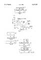
- FIG. 1Shows a preferred embodiment of the present invention showing double sided interdiffusion of MCT mounted to a ROIC;
- FIG. 2Shows the stress curve for MCT and a typical thermoplastic
- FIGS. 3a-3dIllustrate the sequence of processing steps for a method of fabricating a MCT structure according to the present invention.
- FIGS. 1-3 of the drawingslike numerals are used for like and corresponding parts of the various drawings.
- integrated circuits diesare usually mounted in packages or multi-chip modules using epoxy as an adhesive. Since epoxies are thermoset, i.e. their polymer chains are cross linked when heated and do not soften significantly after setting, subsequent thermal processes will induce compressive or tensile stress if the two mated parts have different coefficients of thermal expansion.
- the present inventionemploys thermoplastic as a die adhesive to avoid excessive stresses caused by a mismatch in coefficient of thermal expansion.
- FIG. 1there is shown a completed structure of an embodiment of the present invention, wherein a MCT 10 chip which has double sided CdTe interdiffusion 12 for surface passivation is mounted with thermoplastic 16 to a silicon ROIC 14.
- FIGS. 3a-3dthere is shown a method of forming an embodiment of the present invention which is shown in the completed structure of FIG. 1.
- FIG. 2represents the stress curve of a MCT chip epoxy mounted to a ROIC. If the epoxy is cured at 60° C., heating or cooling from this temperature will result in thermal stress in the MCT at a rate of about 0.1 MPa/°C. as depicted with small dashed lines 13 in FIG. 2.
- the solid curved line in FIG. 2represents the yield strength of the MCT. The yield strength is exceeded by the epoxy bonded device when the hybrid device is heated to 120° C., resulting in damage to the MCT.
- the dotted lined curve 16 in FIG. 2represents the thermal stress in the MCT as a function of temperature when the thermoplastic adhesive is used to bond the hybrid device. It can be seen from curve 15 in FIG.
- thermoplastic devicedoes not exceed the yield strength of the MCT even when heated to 300° C.
- the yield strengthis not exceeded in this case because the thermoplastic softens when its temperature reaches its softening temperature and relieves the thermal stress in the hybrid device.
- FIG. 3ashows a layer of MCT 10 preferably grown by Liquid Phase Epitaxy (LPE) on a cadmium zinc telluride (CZT) substrate 18.
- LPELiquid Phase Epitaxy
- CZTcadmium zinc telluride
- FIG. 3bshows a ROIC coated with a thermoplastic adhesive 16.
- the MCTis mounted to the ROIC as shown in FIG. 3c using a thermoplastic adhesive 16.
- a second passivation layer of CdTeis deposited on the top side of the MCT.
- the MCT with the CdTe layersis then annealed to interdiffusion the CdTe into the MCT.
- the ROIC module with the MCT as shown in FIG. 3dis then ready for processing to create the FPA.
- a layer of MCT 10is grown by Liquid Phase Epitaxy (LPE) on a cadmium zinc telluride (CZT) substrate 16 to a thickness of between 10 and 200 ⁇ m.
- LPELiquid Phase Epitaxy
- CZTcadmium zinc telluride
- the MCTis planarized, preferably by diamond point turning (DPT) to remove irregularities caused by the LPE process.
- DPTdiamond point turning
- the MCT slice formed by LPEis preferably wax mounted to a silicon carrier, LPE side up, to facilitate processing.
- the top surface of the MCTis prepared for passivation by bromide polishing using a solution of 1/4% bromine in methanol.
- the MCTis further prepared for passivation by rinsing on a spiner.
- a layer of CdTe 12is deposited on the MCT 10 for passivation as shown in FIG. 3b.
- Deposition of the CdTeis preferably accomplished by evaporating 5000 ⁇ of 30° C. CdTe onto the surface of the MCT followed by deposition of 3000 ⁇ of sputtered ZnS.
- the purpose of the ZnSis a diffusion barrier for contaminants and mercury during anneal.
- the MCTis then annealed to diffuse the CdTe into the MCT at 250-350° C. for 1-4 days. This first anneal may be eliminated and combined with the second anneal step below.
- the MCT 10which has now been passivated on one side is prepared to be mounted to the ROIC, CdTe side down. Prior to mounting the ZnS is preferably removed from the surface of the CdTe.
- the MCTis preferably mounted to the ROIC as shown in FIG. 3c using polyester or polyamide thermoplastics 16. It was found the viscosity and surface tension of the thermoplastic is sufficient to keep the IC's in place even at temperatures sufficiently above the thermoplastic softening temperature.
- a desirable softening temperatureshould be low enough such that the thermoplastic softens to relieve the thermal stress before yield strengths of the parts are exceeded, but it should not be so low that the bond loses its strength at service temperatures due to softening.
- a preferred softening temperatureis between 100 and 150° C.
- the steps in mounting the MCT to the ROICpreferably include the following steps:
- the CZT 18is preferably removed by diamond point turning (DPT) and the MCT is preferably ground to near the desired final thickness.
- the MCTis preferably ground during the DPT process to about 20 ⁇ m in thickness.
- the MCTis then polished to its final preferred thickness of between 6 and 8 ⁇ m, preferably with 1/4% bromine methanol.
- the top surface of the MCTcan now be passivated with CdTe.
- a layer of CdTe 12is deposited on the top surface of the MCT 10 for passivation as shown in FIG. 3d.
- Deposition of the CdTeis preferably accomplished by evaporating 5000 ⁇ of 30° C. CdTe onto the surface of the MCT.
- the MCTis then annealed to diffuse the CdTe into the MCT at 150-250° C. for 1-4 days.
- the MCTis now as shown in FIG. 2d mounted to the ROIC and is ready for processing to create the FPA by fabricating an array of photodetectors in the MCT and connecting them to the ROIC as discussed above.
Landscapes
- Engineering & Computer Science (AREA)
- Computer Hardware Design (AREA)
- Microelectronics & Electronic Packaging (AREA)
- Power Engineering (AREA)
- Solid State Image Pick-Up Elements (AREA)
Abstract
Description
TABLE ______________________________________ Preferred or Drawing Specific Element Examples Generic Term Other Alternate Examples ______________________________________ 10 MCT Chip Die (Mercury Cadmium Telluride) 12CdTe Passivation Layer 14 ROIC (Read Carrier Chip Multi-Chip Module Out or Substrate Integrated Circuit) 16Thermoplastic Thermoplastic 18 CZT Substrate ______________________________________
Claims (11)
Priority Applications (1)
| Application Number | Priority Date | Filing Date | Title |
|---|---|---|---|
| US09/304,953US6127203A (en) | 1996-08-30 | 1999-05-05 | Thermoplastic mounting of a semiconductor die to a substrate having a mismatched coefficient of thermal expansion |
Applications Claiming Priority (2)
| Application Number | Priority Date | Filing Date | Title |
|---|---|---|---|
| US08/707,815US5959340A (en) | 1995-09-05 | 1996-08-30 | Thermoplastic mounting of a semiconductor die to a substrate having a mismatched coefficient of thermal expansion |
| US09/304,953US6127203A (en) | 1996-08-30 | 1999-05-05 | Thermoplastic mounting of a semiconductor die to a substrate having a mismatched coefficient of thermal expansion |
Related Parent Applications (1)
| Application Number | Title | Priority Date | Filing Date |
|---|---|---|---|
| US08/707,815DivisionUS5959340A (en) | 1995-09-05 | 1996-08-30 | Thermoplastic mounting of a semiconductor die to a substrate having a mismatched coefficient of thermal expansion |
Publications (1)
| Publication Number | Publication Date |
|---|---|
| US6127203Atrue US6127203A (en) | 2000-10-03 |
Family
ID=24843268
Family Applications (1)
| Application Number | Title | Priority Date | Filing Date |
|---|---|---|---|
| US09/304,953Expired - Fee RelatedUS6127203A (en) | 1996-08-30 | 1999-05-05 | Thermoplastic mounting of a semiconductor die to a substrate having a mismatched coefficient of thermal expansion |
Country Status (1)
| Country | Link |
|---|---|
| US (1) | US6127203A (en) |
Cited By (9)
| Publication number | Priority date | Publication date | Assignee | Title |
|---|---|---|---|---|
| US6621071B2 (en)* | 2001-09-07 | 2003-09-16 | Raytheon Co. | Microelectronic system with integral cryocooler, and its fabrication and use |
| US20040061056A1 (en)* | 2002-09-26 | 2004-04-01 | Barton Jeffrey B. | Infrared detector array with improved spectral range and method for making the same |
| US20040150115A1 (en)* | 2002-12-05 | 2004-08-05 | Seiko Epson Corporation | Electronic device, method of manufacturing the same, and electronic instrument |
| GB2433648A (en)* | 2005-12-21 | 2007-06-27 | Durham Scient Crystals Ltd | Radiation detector formed by deposition of bulk semiconductor crystal layers |
| US20090053453A1 (en)* | 2005-12-21 | 2009-02-26 | Durham Scientific Crystals Limited | Semiconductor device and method of manufacture thereof |
| US9647194B1 (en) | 2006-08-25 | 2017-05-09 | Hypres, Inc. | Superconductive multi-chip module for high speed digital circuits |
| US10374000B2 (en) | 2013-09-23 | 2019-08-06 | Teledyne Scientific & Imaging, Llc | Thermal-contraction matched hybrid device package |
| CN110634991A (en)* | 2019-09-02 | 2019-12-31 | 中国电子科技集团公司第十一研究所 | Preparation method of silicon-based mercury cadmium telluride chip and mercury cadmium telluride infrared detector |
| WO2023278003A1 (en)* | 2021-06-29 | 2023-01-05 | Raytheon Company | Low-stress dielectric layer, planarization method, and low-temperature processing for 3d-integrated electrical device |
Citations (9)
| Publication number | Priority date | Publication date | Assignee | Title |
|---|---|---|---|---|
| US4720738A (en)* | 1982-09-08 | 1988-01-19 | Texas Instruments Incorporated | Focal plane array structure including a signal processing system |
| US5144138A (en)* | 1989-10-06 | 1992-09-01 | Texas Instruments Incorporated | Infrared detector and method |
| US5146303A (en)* | 1990-04-05 | 1992-09-08 | General Electric Company | Compact, thermally efficient focal plane array and testing and repair thereof |
| US5318666A (en)* | 1993-04-19 | 1994-06-07 | Texas Instruments Incorporated | Method for via formation and type conversion in group II and group VI materials |
| US5348607A (en)* | 1989-02-21 | 1994-09-20 | General Electric Company | High density interconnect thermoplastic die attach material and solvent die attach processing |
| US5380669A (en)* | 1993-02-08 | 1995-01-10 | Santa Barbara Research Center | Method of fabricating a two-color detector using LPE crystal growth |
| US5391604A (en)* | 1993-07-30 | 1995-02-21 | Diemat, Inc. | Adhesive paste containing polymeric resin |
| US5420445A (en)* | 1993-02-22 | 1995-05-30 | Texas Instruments Incorporated | Aluminum-masked and radiantly-annealed group II-IV diffused region |
| US5608208A (en)* | 1994-02-08 | 1997-03-04 | Technion Research & Development Foundation Ltd. | Single layer planar HgCdTe photovoltaic infrared detector with heterostructure passivation and p-on-n homojunction |
- 1999
- 1999-05-05USUS09/304,953patent/US6127203A/ennot_activeExpired - Fee Related
Patent Citations (10)
| Publication number | Priority date | Publication date | Assignee | Title |
|---|---|---|---|---|
| US4720738A (en)* | 1982-09-08 | 1988-01-19 | Texas Instruments Incorporated | Focal plane array structure including a signal processing system |
| US5348607A (en)* | 1989-02-21 | 1994-09-20 | General Electric Company | High density interconnect thermoplastic die attach material and solvent die attach processing |
| US5144138A (en)* | 1989-10-06 | 1992-09-01 | Texas Instruments Incorporated | Infrared detector and method |
| US5146303A (en)* | 1990-04-05 | 1992-09-08 | General Electric Company | Compact, thermally efficient focal plane array and testing and repair thereof |
| US5380669A (en)* | 1993-02-08 | 1995-01-10 | Santa Barbara Research Center | Method of fabricating a two-color detector using LPE crystal growth |
| US5420445A (en)* | 1993-02-22 | 1995-05-30 | Texas Instruments Incorporated | Aluminum-masked and radiantly-annealed group II-IV diffused region |
| US5462882A (en)* | 1993-02-22 | 1995-10-31 | Texas Instruments Incorporated | Masked radiant anneal diffusion method |
| US5318666A (en)* | 1993-04-19 | 1994-06-07 | Texas Instruments Incorporated | Method for via formation and type conversion in group II and group VI materials |
| US5391604A (en)* | 1993-07-30 | 1995-02-21 | Diemat, Inc. | Adhesive paste containing polymeric resin |
| US5608208A (en)* | 1994-02-08 | 1997-03-04 | Technion Research & Development Foundation Ltd. | Single layer planar HgCdTe photovoltaic infrared detector with heterostructure passivation and p-on-n homojunction |
Non-Patent Citations (2)
| Title |
|---|
| Definition of "epoxy," Webster's II New Riverside . . . Dictionary, 1984, p. 439. |
| Definition of epoxy, Webster s II New Riverside . . . Dictionary , 1984, p. 439.* |
Cited By (21)
| Publication number | Priority date | Publication date | Assignee | Title |
|---|---|---|---|---|
| US6621071B2 (en)* | 2001-09-07 | 2003-09-16 | Raytheon Co. | Microelectronic system with integral cryocooler, and its fabrication and use |
| US20060180752A1 (en)* | 2001-09-07 | 2006-08-17 | Sobel Larry D | Stacked-plate gas-expansion cooler assembly, fabrication method, and use |
| US7178345B2 (en) | 2001-09-07 | 2007-02-20 | Ratheon Company | Stacked-plate gas-expansion cooler assembly, fabrication method, and use |
| US20040061056A1 (en)* | 2002-09-26 | 2004-04-01 | Barton Jeffrey B. | Infrared detector array with improved spectral range and method for making the same |
| US6852976B2 (en)* | 2002-09-26 | 2005-02-08 | Indigo Systems Corporation | Infrared detector array with improved spectral range and method for making the same |
| US20040150115A1 (en)* | 2002-12-05 | 2004-08-05 | Seiko Epson Corporation | Electronic device, method of manufacturing the same, and electronic instrument |
| US6967410B2 (en)* | 2002-12-05 | 2005-11-22 | Seiko Epson Corporation | Electronic device, method of manufacturing the same, and electronic instrument |
| US20100327277A1 (en)* | 2005-12-21 | 2010-12-30 | Durham Scientific Crystals Limited | Semiconductor device with a bulk single crystal on a substrate |
| US8968469B2 (en) | 2005-12-21 | 2015-03-03 | Kromek Limited | Semiconductor device and method of manufacture thereof |
| US20090053453A1 (en)* | 2005-12-21 | 2009-02-26 | Durham Scientific Crystals Limited | Semiconductor device and method of manufacture thereof |
| GB2433648A (en)* | 2005-12-21 | 2007-06-27 | Durham Scient Crystals Ltd | Radiation detector formed by deposition of bulk semiconductor crystal layers |
| US20110024877A1 (en)* | 2005-12-21 | 2011-02-03 | Durham Scientific Crystals Limited | Semiconductor device and method of manufacture thereof |
| US8093095B2 (en) | 2005-12-21 | 2012-01-10 | Kromek Limited | Semiconductor device with a bulk single crystal on a substrate |
| US8093671B2 (en) | 2005-12-21 | 2012-01-10 | Kromek Limited | Semiconductor device with a bulk single crystal on a substrate |
| US20080315342A1 (en)* | 2005-12-21 | 2008-12-25 | Durham Scientific Crystals Limited | Semiconductor Device with a Bulk Single Crystal on a Substrate |
| US9647194B1 (en) | 2006-08-25 | 2017-05-09 | Hypres, Inc. | Superconductive multi-chip module for high speed digital circuits |
| US10373928B1 (en) | 2006-08-25 | 2019-08-06 | Hypres, Inc. | Method for electrically interconnecting at least two substrates and multichip module |
| US10374000B2 (en) | 2013-09-23 | 2019-08-06 | Teledyne Scientific & Imaging, Llc | Thermal-contraction matched hybrid device package |
| CN110634991A (en)* | 2019-09-02 | 2019-12-31 | 中国电子科技集团公司第十一研究所 | Preparation method of silicon-based mercury cadmium telluride chip and mercury cadmium telluride infrared detector |
| CN110634991B (en)* | 2019-09-02 | 2021-07-02 | 中国电子科技集团公司第十一研究所 | A kind of silicon-based mercury cadmium telluride chip preparation method and mercury cadmium telluride infrared detector |
| WO2023278003A1 (en)* | 2021-06-29 | 2023-01-05 | Raytheon Company | Low-stress dielectric layer, planarization method, and low-temperature processing for 3d-integrated electrical device |
Similar Documents
| Publication | Publication Date | Title |
|---|---|---|
| US5380669A (en) | Method of fabricating a two-color detector using LPE crystal growth | |
| US5185648A (en) | Plural-wavelength infrared detector devices | |
| US7820525B2 (en) | Method for manufacturing hybrid image sensors | |
| US20010029061A1 (en) | Insulator/metal bonding island for active-area silver epoxy bonding | |
| US5236871A (en) | Method for producing a hybridization of detector array and integrated circuit for readout | |
| IL99856A (en) | Electro-optical detector array and method of making same | |
| US5959340A (en) | Thermoplastic mounting of a semiconductor die to a substrate having a mismatched coefficient of thermal expansion | |
| US4422091A (en) | Backside illuminated imaging charge coupled device | |
| US6127203A (en) | Thermoplastic mounting of a semiconductor die to a substrate having a mismatched coefficient of thermal expansion | |
| Rogalski | New trends in semiconductor infrared detectors | |
| KR102690630B1 (en) | Semiconductor device with aluminum nitride anti-deflection layer | |
| US5585624A (en) | Apparatus and method for mounting and stabilizing a hybrid focal plane array | |
| US5696377A (en) | Hybrid infrared ray detector with an improved bonding structure between an Si-substrate having integrated circuits and an HgCdTe layer having two-dimensional photodiode arrays and method for fabricating the same | |
| US20110233609A1 (en) | Method for Producing Infrared-Photosensitive Matrix Cells Adhering to an Optically Transparent Substrate by Molecular Adhesion, and Related Sensor | |
| WO1994017557A1 (en) | Thermally matched readout/detector assembly and method for fabricating same | |
| JPH0536966A (en) | Semiconductor device | |
| US5846850A (en) | Double sided interdiffusion process and structure for a double layer heterojunction focal plane array | |
| US5600140A (en) | Imbalanced composite focal plane array | |
| US5599733A (en) | Method using cadmium-rich CdTe for lowering the metal vacancy concentrations of HgCdTe surfaces | |
| Vasilyev et al. | Focal plane arrays based on HgCdTe epitaxial layers MBE-grown on GaAs substrates | |
| Alchalabi et al. | Monolithic heteroepitaxial PbTe-on-Si infrared focal plane array with 96× 128 pixels | |
| JP7666876B2 (en) | Low stress dielectric layers, planarization methods, and low temperature processing for 3D integrated electrical devices | |
| Zanio et al. | HgCdTe on GaAs/Si for mid‐wavelength infrared focal plane arrays | |
| JP3577368B2 (en) | Hybrid type infrared detector | |
| JP3114759B2 (en) | Semiconductor device |
Legal Events
| Date | Code | Title | Description |
|---|---|---|---|
| AS | Assignment | Owner name:FIRST UNION NATIONAL BANK, NORTH CAROLINA Free format text:SECURITY INTEREST;ASSIGNOR:DRS TECHNOLOGIES, INC.;REEL/FRAME:013463/0227 Effective date:20010928 | |
| REMI | Maintenance fee reminder mailed | ||
| LAPS | Lapse for failure to pay maintenance fees | ||
| STCH | Information on status: patent discontinuation | Free format text:PATENT EXPIRED DUE TO NONPAYMENT OF MAINTENANCE FEES UNDER 37 CFR 1.362 | |
| FP | Lapsed due to failure to pay maintenance fee | Effective date:20041003 | |
| AS | Assignment | Owner name:WACHOVIA BANK, NATIONAL ASSOCIATION, NORTH CAROLIN Free format text:PATENT SECURITY AGREEMENT;ASSIGNOR:DRS TECHNOLOGIES, INC.;REEL/FRAME:017286/0342 Effective date:20060131 | |
| AS | Assignment | Owner name:WACHOVIA BANK, NATIONAL ASSOCIATION, NORTH CAROLIN Free format text:PATENT SECURITY AGREEMENT;ASSIGNOR:DRS SENSORS & TARGETING SYSTEMS, INC.;REEL/FRAME:019580/0785 Effective date:20060615 | |
| AS | Assignment | Owner name:DRS SENSORS & TARGETING SYSTEMS, INC.,TEXAS Free format text:RELEASE BY SECURED PARTY;ASSIGNOR:WELLS FARGO BANK, N.A.;REEL/FRAME:024611/0597 Effective date:20100607 |