US6126798A - Electroplating anode including membrane partition system and method of preventing passivation of same - Google Patents
Electroplating anode including membrane partition system and method of preventing passivation of sameDownload PDFInfo
- Publication number
- US6126798A US6126798AUS08/969,196US96919697AUS6126798AUS 6126798 AUS6126798 AUS 6126798AUS 96919697 AUS96919697 AUS 96919697AUS 6126798 AUS6126798 AUS 6126798A
- Authority
- US
- United States
- Prior art keywords
- anode
- membrane
- cup
- ion source
- source material
- Prior art date
- Legal status (The legal status is an assumption and is not a legal conclusion. Google has not performed a legal analysis and makes no representation as to the accuracy of the status listed.)
- Expired - Lifetime
Links
- 239000012528membraneSubstances0.000titleclaimsabstractdescription96
- 238000009713electroplatingMethods0.000titleclaimsdescription23
- 238000002161passivationMethods0.000titleclaimsdescription11
- 238000000034methodMethods0.000titleclaimsdescription7
- 238000005192partitionMethods0.000title1
- 238000007747platingMethods0.000claimsabstractdescription124
- 239000000463materialSubstances0.000claimsabstractdescription45
- 239000010949copperSubstances0.000claimsdescription7
- -1polypropylenePolymers0.000claimsdescription6
- RYGMFSIKBFXOCR-UHFFFAOYSA-NCopperChemical compound[Cu]RYGMFSIKBFXOCR-UHFFFAOYSA-N0.000claimsdescription4
- 239000004743PolypropyleneSubstances0.000claimsdescription4
- RTAQQCXQSZGOHL-UHFFFAOYSA-NTitaniumChemical compound[Ti]RTAQQCXQSZGOHL-UHFFFAOYSA-N0.000claimsdescription4
- 229910052802copperInorganic materials0.000claimsdescription4
- 229920001155polypropylenePolymers0.000claimsdescription4
- 239000004020conductorSubstances0.000claimsdescription3
- 239000008187granular materialSubstances0.000claimsdescription3
- 239000004698PolyethyleneSubstances0.000claimsdescription2
- 229920000573polyethylenePolymers0.000claimsdescription2
- 239000000758substrateSubstances0.000claims3
- 229920000642polymerPolymers0.000claims2
- 235000012431wafersNutrition0.000description57
- 150000002500ionsChemical class0.000description30
- 239000007789gasSubstances0.000description11
- 239000000356contaminantSubstances0.000description7
- 230000004907fluxEffects0.000description7
- 235000014676Phragmites communisNutrition0.000description6
- 230000005684electric fieldEffects0.000description6
- 101100493712Caenorhabditis elegans bath-42 geneProteins0.000description5
- 238000003491arrayMethods0.000description5
- 238000011109contaminationMethods0.000description5
- VLLVVZDKBSYMCG-UHFFFAOYSA-N1,3,5-trichloro-2-(2-chlorophenyl)benzeneChemical compoundClC1=CC(Cl)=CC(Cl)=C1C1=CC=CC=C1ClVLLVVZDKBSYMCG-UHFFFAOYSA-N0.000description4
- 238000004140cleaningMethods0.000description4
- 238000000151depositionMethods0.000description3
- 230000000694effectsEffects0.000description3
- 239000012777electrically insulating materialSubstances0.000description3
- 239000004065semiconductorSubstances0.000description3
- 239000010936titaniumSubstances0.000description3
- 229910052719titaniumInorganic materials0.000description3
- QVGXLLKOCUKJST-UHFFFAOYSA-Natomic oxygenChemical compound[O]QVGXLLKOCUKJST-UHFFFAOYSA-N0.000description2
- 238000007796conventional methodMethods0.000description2
- 230000008021depositionEffects0.000description2
- 238000003487electrochemical reactionMethods0.000description2
- 239000001301oxygenSubstances0.000description2
- 229910052760oxygenInorganic materials0.000description2
- 229920013632RytonPolymers0.000description1
- 239000004736Ryton®Substances0.000description1
- 239000004809TeflonSubstances0.000description1
- 229920006362Teflon®Polymers0.000description1
- 238000009825accumulationMethods0.000description1
- 239000010405anode materialSubstances0.000description1
- 230000015572biosynthetic processEffects0.000description1
- 238000010276constructionMethods0.000description1
- 238000004090dissolutionMethods0.000description1
- 230000002708enhancing effectEffects0.000description1
- 238000001914filtrationMethods0.000description1
- 229910000765intermetallicInorganic materials0.000description1
- WABPQHHGFIMREM-AKLPVKDBSA-Nlead-210Chemical compound[210Pb]WABPQHHGFIMREM-AKLPVKDBSA-N0.000description1
- WABPQHHGFIMREM-BKFZFHPZSA-Nlead-212Chemical compound[212Pb]WABPQHHGFIMREM-BKFZFHPZSA-N0.000description1
- 239000007788liquidSubstances0.000description1
- 238000004519manufacturing processMethods0.000description1
- 150000003071polychlorinated biphenylsChemical class0.000description1
- 239000004800polyvinyl chlorideSubstances0.000description1
- 229920000131polyvinylidenePolymers0.000description1
- 230000000284resting effectEffects0.000description1
- 238000007493shaping processMethods0.000description1
- 239000007787solidSubstances0.000description1
- BFKJFAAPBSQJPD-UHFFFAOYSA-NtetrafluoroetheneChemical compoundFC(F)=C(F)FBFKJFAAPBSQJPD-UHFFFAOYSA-N0.000description1
Images


Classifications
- C—CHEMISTRY; METALLURGY
- C25—ELECTROLYTIC OR ELECTROPHORETIC PROCESSES; APPARATUS THEREFOR
- C25D—PROCESSES FOR THE ELECTROLYTIC OR ELECTROPHORETIC PRODUCTION OF COATINGS; ELECTROFORMING; APPARATUS THEREFOR
- C25D17/00—Constructional parts, or assemblies thereof, of cells for electrolytic coating
- C25D17/10—Electrodes, e.g. composition, counter electrode
- C—CHEMISTRY; METALLURGY
- C25—ELECTROLYTIC OR ELECTROPHORETIC PROCESSES; APPARATUS THEREFOR
- C25D—PROCESSES FOR THE ELECTROLYTIC OR ELECTROPHORETIC PRODUCTION OF COATINGS; ELECTROFORMING; APPARATUS THEREFOR
- C25D17/00—Constructional parts, or assemblies thereof, of cells for electrolytic coating
- C25D17/001—Apparatus specially adapted for electrolytic coating of wafers, e.g. semiconductors or solar cells
- C—CHEMISTRY; METALLURGY
- C25—ELECTROLYTIC OR ELECTROPHORETIC PROCESSES; APPARATUS THEREFOR
- C25D—PROCESSES FOR THE ELECTROLYTIC OR ELECTROPHORETIC PRODUCTION OF COATINGS; ELECTROFORMING; APPARATUS THEREFOR
- C25D17/00—Constructional parts, or assemblies thereof, of cells for electrolytic coating
- C25D17/008—Current shielding devices
Definitions
- the present inventionrelates generally to electroplating and more particularly an anode for an electroplating system.
- electrically conductive leads on the waferare often formed by electroplating (depositing) an electrically conductive material such as copper on the wafer and into patterned trenches.
- Electroplatinginvolves making electrical contact with the wafer surface upon which the electrically conductive layer is to be deposited (hereinafter the "wafer plating surface").
- Currentis then passed through a plating solution (i.e. a solution containing ions of the element being deposited, for example a solution containing Cu ++ ) between an anode and the wafer plating surface (the wafer plating surface being the cathode).
- a plating solutioni.e. a solution containing ions of the element being deposited, for example a solution containing Cu ++
- Insoluble anodestend to evolve oxygen bubbles which adhere to the wafer plating surface. These oxygen bubbles disrupt the flow of ions and electrical current to the wafer plating surface creating nonuniformity in the deposited electrically conductive layer. For this reason, soluble anodes are frequently used.
- Soluble anodesare not without disadvantages.
- One disadvantageis that soluble anodes, by definition, dissolve. As a soluble anode dissolves, it releases particulates into the plating solution. These particulates can contaminate the wafer plating surface, reducing the reliability and yield of the semiconductor devices formed on the wafer.
- One conventional technique of reducing particulate contaminationis to contain the soluble anode in a porous anode bag.
- conventional anode bagsfail to prevent smaller sized particulates from entering the plating solution and contaminating the wafer plating surface.
- filters 60are positioned between anode arrays 20 and a printed circuit board 50 (PCB 50).
- PCB 50printed circuit board 50
- Filters 60allows only ionic material of a relatively small size, for example one micron, to pass from anode arrays 20 to PCB 50. While allowing relatively small size particulates to pass through, filters 60 trap larger sized particulates avoiding contamination of PCB 50 from these larger sized particulates. Over time, however, filters 60 become clogged by these larger sized particulates.
- Reedprovides a counterflow of plating solution through filters 60 in a direction from PCB 50 towards anode arrays 20. This counterflow tends to wash some of the larger sized particulates from filters 60. However, even with the counterflow, eventually filters 60 become clogged. To allow servicing of filters 60, retaining strips 66 and support strips 68 allow filters 60 to be removed and cleaned when filters 60 eventually become clogged.
- filters 60Although providing a convenient means of cleaning filters 60, removal of filters 60 necessarily releases the larger sized particulates from within the vicinity of anode arrays 20 into the entire system and, in particular, into the vicinity where PCBs 50 are electroplated. Even after filters 60 are cleaned and replaced, this contamination of the system can cause contamination of a subsequently electroplated PCE 50 reducing the reliability and yield of the printed circuit boards. Further, even with filters 60, particulates accumulate on receptacle 14 in the vicinity of anode arrays 20 and the system must periodically be shut down and drained of plating solution to clean these particulates from receptacle 14.
- a soluble anodechanges shape as it dissolves, resulting in variations in the electric field between the soluble anode and the wafer.
- the thickness of the electrically conductive layer deposited on the wafer plating surfacedepends upon the electric field.
- variations in the shape of the soluble anoderesult in variations in the thickness of the deposited electrically conductive layer across the wafer plating surface.
- anode passivationAnother disadvantage of soluble anodes is passivation. As is well known to those skilled in the art, the mechanism by which anode passivation occurs depends upon a variety of factors including the process conditions, plating solution and anode material. Generally, anode passivation inhibits dissolution of the anode while simultaneously preventing electrical current from being passed through the anode and should be avoided.
- an anodein accordance with the present invention includes an anode cup, a membrane and ion source material.
- the anode source materialis located in an enclosure formed by the anode cup and membrane.
- the anode cup and membraneboth have central apertures through which a jet (a tube) is passed. During use, plating solution flows through the jet.
- plating solution from the jetis directed at the center of the wafer being electroplated. This enhances removal of gas bubbles entrapped on the wafer plating surface and improves the uniformity of the deposited electrically conductive layer on the wafer.
- the membranehas a porosity sufficient to allow ions from the ion source material, and hence electrical current, to flow through the membrane. Although allowing electrical current to pass, the membrane has a high electrical resistance which produces a voltage drop across the membrane during use. This high electrical resistance redistributes localized high electrical currents over larger areas improving the uniformity of the electric current flux to the wafer which, in turn, improves the uniformity of the deposited electrically conductive layer on the wafer.
- the membraneIn addition to having a porosity sufficient to allow electrical current to pass, the membrane also has a porosity sufficient to allow plating solution to flow through the membrane. However, to prevent particulates generated by the ion source material from passing through the membrane and contaminating the wafer, the porosity of the membrane prevents contaminant particulates from passing through the membrane.
- the anodewhen the membrane becomes clogged with particulates, the anode can be readily removed from the electroplating system. After removal of the anode, the membrane can be separated from the anode cup and cleaned or replaced.
- cleaning of the membraneis accomplished outside of the plating bath and, accordingly, without releasing particulates from inside of the anode into the plating bath.
- the jetincludes a plating solution inlet through which plating solution flows from the jet into the enclosure formed by the anode cup and membrane and across the ion source material.
- the flow of plating solution across the ion source materialprevents anode passivation.
- the plating solutionthen exits the enclosure via two routes. First, some of the plating solution exits through the membrane. As discussed above, contaminant particulates generated as the ion source material dissolves do not pass through the membrane and accordingly do not contaminate the wafer. Second, some of the plating solution exits through outlets located at the top of a wall section of the anode cup.
- outletsare plumbed to an overflow receiver and thus the plating solution which flows through these outlets does not enter the plating bath and does not contaminate the wafer. Further, by locating these outlets at the top of the wall section of the anode cup, gas bubbles entrapped under the membrane are entrained with the exiting plating solution and readily removed from the anode.
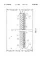
- FIG. 1is a diagrammatic view of an electroplating apparatus having a wafer mounted therein in accordance with the present invention.
- FIG. 2is a cross-sectional view of an anode in accordance with the present invention.
- FIGS. 3 and 4are cross-sectional views of anodes in accordance with alternative embodiments of the present invention.
- FIG. 1is a diagrammatic view of an electroplating apparatus 30 having a wafer 38 mounted therein in accordance with the present invention.
- Apparatus 30includes a clamshell 32 mounted on a rotatable spindle 40 which allows rotation of clamshell 32.
- Clamshell 32comprises a cone 34, a cup 36 and a flange 48.
- Flange 48has formed therein a plurality of apertures 50.
- a clamshell lacking a flange 48 yet in other regards similar to clamshell 32is described in detail in Patton et al., co-filed application Ser. No. 08/969,984, cited above.
- a clamshell including a flange similar to clamshell 32is described in detail in Contolini et al., co-filed application Ser. No. 08/990,120, cited above.
- wafer 38is mounted in cup 36. Clamshell 32 and hence wafer 38 are then placed in a plating bath 42 containing a plating solution. As indicated by arrow 46, the plating solution is continually provided to plating bath 42 by a pump 44. Generally, the plating solution flows upwards to the center of wafer 38 and then radially outward and across wafer 38 through apertures 50 as indicated by arrows 52. Of importance, by directing the plating solution towards the center of wafer 38, any gas bubbles entrapped on wafer 38 are quickly removed through apertures 50. Gas bubble removal is further enhanced by rotating clamshell 32 and hence wafer 38.
- the plating solutionthen overflows plating bath 42 to an overflow reservoir 56 as indicated by arrows 54.
- the plating solutionis then filtered (not shown) and returned to pump 44 as indicated by arrow 58 completing the recirculation of the plating solution.
- a DC power supply 60has a negative output lead 210 electrically connected to wafer 38 through one or more slip rings, brushes and contacts (not shown).
- the positive output lead 212 of power supply 60is electrically connected to an anode 62 located in plating bath 42.
- power supply 60biases wafer 38 to have a negative potential relative to anode 62 causing an electrical current to flow from anode 62 to wafer 38.
- electrical currentflows in the same direction as the net positive ion flux and opposite the net electron flux.
- the electrically conductive layere.g. copper
- Shields 53 and 55are provided to shape the electric field between anode 62 and wafer 38. The use and construction of shields are further described in Reid et al., co-filed application Ser. No. 08/969,267, cited above.
- Jet 200typically consists of a tube formed of an electrically insulating material.
- Anode 62Acomprises an anode cup 202, contact 204, ion source material 206, and a membrane 208.
- Anode cup 202is typically an electrically insulating material such as polyvinyl chloride (PVC), polypropylene or polyvinylidene flouride (PVDF).
- Anode cup 202comprises a disk shaped base section 216 having a central aperture 214 through which jet 200 passes.
- An O-ring 310forms the seal between jet 200 and base section 216 of anode cup 202.
- Anode cup 202further comprises a cylindrical wall section 218 integrally attached at one end (the bottom) to base section 216.
- Contact 204is typically an electrically conductive relatively inert material such as titanium. Further, contact 204 can be fashioned in a variety of forms, e.g. can be a plate with raised perforations or, as illustrated in FIG. 2, a mesh. Contact 204 rests on base section 216 of anode cup 202. Positive output lead 212 from power supply 60 (see FIG. 1) is formed of an electrically conductive relatively inert material such as titanium. Lead 212 is attached, typically bolted, to a rod 270 which is also formed of an electrically conductive relatively inert material such as titanium. Rod 270 passes through anode cup 202 to make the electrical connection with contact 204.
- Ion source material 206for example copper.
- Ion source material 206comprises a plurality of granules. These granules can be fashioned in a variety of shapes such as in a spherical, nugget, flake or pelletized shape. In one embodiment, copper balls having a diameter in the range of 1.0 centimeters to 2.54 centimeters are used.
- ion source material 206comprises an single integral piece such as a solid disk of material.
- Ion source material 206is contained in an enclosure formed by anode cup 202, membrane 208 and jet 200. More particularly, membrane 208 is attached, typically welded, to a seal ring 312 at a central aperture 207 of membrane 208 and to a seal ring 314 at its outer circumference. Seal rings 312, 314 are formed of materials similar to those discussed above for anode cup 202. Seal ring 312 forms a seal with jet 200 by an O-ring 316 and seal ring 314 forms a seal with a second end (the top) of wall section 218 of anode cup 202 by an O-ring 318.
- membrane 208By attaching membrane 208 to seal rings 312, 314, membrane 208 forms a seal at its outer circumference with the top of wall section 218 of anode cup 202 and also forms a seal with jet 200 at central aperture 207 of membrane 208.
- Suitable examples of membrane 208include: napped polypropylene available from Anode Products, Inc. located in Illinois; spunbond snowpro polypropylene and various polyethylene, RYTON, and TEFLON materials in felt, monofilament, filament and spun forms available from various suppliers including Snow Filtration, 6386 Gano Rd., West Chester, Ohio.
- membrane 208is itself formed of a material having a sufficient rigidity to form a pressure fit with wall section 218 and jet 200 and seal rings 312, 314 are not provided.
- Membrane 208has a porosity sufficient to allow ions from ion source material 206, and hence electrical current, to flow through membrane 208. Although allowing electrical current to flow through, membrane 208 has a high electrical resistance which produces a voltage drop across membrane 208 from lower surface 209 to upper surface 211. This advantageously minimizes variations in the electric field from ion source material 206 as it dissolves and changes shape.
- a region of ion source material 206 having a high electrical conductivity relative to the remainder of ion source material 206would support a relatively high electrical current. This in turn would provide a relatively high electric current flux to the portion of the wafer directly above this region of ion source material 206, resulting in a greater thickness of the deposited electrically conductive layer on this portion of the wafer.
- the relatively high electrical current from this region of ion source material 206redistributes over a larger area to find the path of least resistance through membrane 208. Redistributing the relatively high electrical current over a larger area improves the uniformity of the electric current flux to the wafer which, in turn, improves the uniformity of the deposited electrically conductive layer.
- membrane 208In addition to having a porosity sufficient to allow electrical current to flow through, membrane 208 also has a porosity sufficient to allow plating solution to flow through membrane 208, i.e. has a porosity sufficient to allow liquid to pass through membrane 208.
- the porosity of membrane 208prevents large size particulates from passing through membrane 208.
- anode 62Acan readily be removed from plating bath 42A. After removal of anode 62A, membrane 208 is separated from anode cup 202 and cleaned or replaced.
- cleaning of membrane 208is accomplished outside of plating bath 42A and, accordingly, without releasing particulates from inside of anode 62A into plating bath 42A. This is in contrast to Reed (cite above) wherein cleaning of the membrane necessarily releases particulates into the bulk of the plating solution.
- use of anode 62A including anode cup 202 and membrane 208prevents particulate accumulation anywhere on plating bath 42A.
- plating solutionis directed into the enclosure formed by anode cup 202 and membrane 208 and across ion source material 206.
- a flow of plating solution across an anodeprevents anode passivation.
- the flow of plating solution into anode cup 202is provided at several locations.
- jet 200is fitted with a plating solution inlet 220 located between membrane 208 and base section 216. A portion of the plating solution flowing through jet 200 is diverted through inlet 220 and into anode cup 202. To prevent inadvertent backflow of plating solution and particulates from anode cup 202 into jet 200, inlet 220 is fitted with a check valve which allows the plating solution only to flow from jet 200 to anode cup 202 and not vice versa.
- Jet 200is also provided with a plating solution outlet 224 which is connected by a tube 230 to an inlet 228 on base section 216 of anode cup 202. In this manner, a portion of the plating solution from jet 200 is directed into the bottom of anode cup 202.
- Outlet 224is fitted with a check valve to prevent backflow of plating solution and particulates from anode cup 202 into jet 200.
- Jet 200is also provided with an outlet 232 connected by a tube 234 to an inlet 236 on wall section 218 of anode cup 202. In this manner, a portion of the plating solution from jet 200 is directed into the side of anode cup 202. Outlet 232 is fitted with a check valve to prevent backflow of plating solution and particulates from anode cup 202 into jet 200.
- inlets 228, 236 on anode cup 202are connected to outlets 224, 232 on jet 200, respectively, in other embodiments (not shown), inlets 228, 236 are connected to an alternative source of plating solution.
- inlets 228, 236are connected to a pump which pumps plating solution to inlets 228, 236 through tubing.
- plating solutionis provided to anode cup 202 from inlets 220, 228, 236, in other embodiments (not shown), only one or more of inlets 220, 228 and 236 are provided.
- solution flowis directed into anode cup 202 through inlet 220 only and inlets 228, 236 (and corresponding outlets 224, 232, check valves and tubes 230, 234, respectively) are not provided.
- a plurality of inlets 220, 228, 236can be provided.
- the plating solution introduced into anode cup 202then flows out of anode cup 202 via two routes.
- some of the plating solutionflows through membrane 208 and into plating bath 42A.
- the porosity of membrane 208allows plating solution to pass through yet prevents particulates over a certain size from passing through (hereinafter referred to as contaminant particulates).
- contaminant particulates generated as ion source material 206dissolves do not pass through membrane 208 and into plating bath 42A and accordingly do not contaminate the wafer being electroplated. This is in contrast to conventional anode bags which allow unacceptably large (e.g. greater than 1.0 ⁇ m) particulates to pass through.
- plating solutionexits through outlets 240, 242 of anode cup 202. From outlets 240, 242, the plating solution flows through tubes 244, 246, though outlets 248, 250 of plating bath 42A and into overflow reservoir 56A. Check valves (not shown) can be provided to prevent backflow of plating solution from overflow reservoir 56A to anode cup 202. From overflow reservoir 56A, the plating solution is filtered to remove particulates including contaminant particulates and then returned to plating bath 42A and jet 200.
- outlets 240, 242support a sufficient flow of plating solution through anode cup 202 to prevent anode passivation to the extent that membrane 208 does not.
- Gas bubble removalis further enhanced by shaping membrane 208 as a frustum of an inverted right circular cone having a base at wall section 218 and an apex at jet 200. More particularly, by having the distance A between membrane 208 and base section 216 at wall section 218 greater than the distance B between membrane 208 and base section 216 at jet 200, gas bubbles entrapped under membrane 208 tend to move across membrane 208 from jet 200 to wall section 218. At wall section 218, these gas bubbles become entrained with the plating solution flowing through outlets 240, 242 and are removed into overflow reservoir 56A. Advantageously, these gas bubbles do not enter plating bath 42A and travel to the wafer and accordingly do not create nonuniformity in the deposited electrically conductive layer on the wafer.
- FIG. 3is a cross-sectional view of an anode 62B and jet 200B in accordance with an alternative embodiment of the present invention.
- anode cup 202Bhas a perforated base section 216B comprising a plurality of apertures 256 extending from a lower surface 219 to an upper surface 221 of perforated base section 216B.
- Anode 62Bfurther comprises a filter sheet 258 on upper surface 221 of perforated base section 216B.
- Contact 204Brests on filter sheet 258 and thereby on perforated base section 216B.
- Filter sheet 258readily allows plating solution to flow through yet prevents contaminant particulates from passing through.
- plating solutionis provided to jet 200B.
- Plating solutionis also provided to plating bath 42B such that the plating solution flows upwards in plating bath 42B towards perforated base section 216B.
- a portion of the plating solutionis diverted around anode cup 202B as indicated by arrows 254. Further, a portion of the plating solution flows through apertures 256, through filter sheet 258 and into anode cup 202B. The plating solution then flows across ion source material 206B preventing anode passivation.
- the plating solutionthen exits anode cup 202B through membrane 208B and outlets 240B, 242B as described above in reference to anode 62A (FIG. 2).
- anode 62B(FIG. 3) allows plating solution to directly enter anode cup 202B without the use of any additional tubing, checkvalves and associated inlets/outlets.
- membranes 208, 208Benable jets 200, 200B, respectively, to pass through the center of the anode.
- thisallows plating solution from jets 200, 200B to be directed at the center of the wafer being electroplated, enhancing removal of gas bubbles entrapped on the wafer plating surface and improving the uniformity of the deposited electrically conductive layer on the wafer.
- Thisis in contrast to conventional anode bags which do not allow the possibility of a configuration which passes a jet through the middle of the anode.
- FIG. 4is a cross-sectional view of an anode 62C and jet 200C in accordance with an alternative embodiment of the present invention.
- jet 200Cdoes not extend through the center of anode 62C but extends horizontally from plating bath 42C and curves upwards to direct plating solution at the center of the wafer (not shown) being electroplated.
- membrane 208Cis a disk shaped integral membrane, i.e. does not have an aperture through which jet 200C passes.
- Anode cup 202Cis provided with a perforated base section 216C having a plurality of apertures 256C. To prevent anode passivation, plating solution, enters anode cup 202C through apertures 256C of perforated base section 216C and then exits through membrane 208C.
- Shield 55Cis formed of an electrically insulating material and reduces the electric field and electric current flux at the edge region of the wafer plating surface. This reduces the thickness of the deposited electrically conductive layer on this edge region of the wafer plating surface thus compensating for the edge effect.
- the edge effectis the tendency of the deposited electrically conductive layer to be thicker at the edge region of the wafer plating surface.
- the edge effectis described in detail in Contolini et al., co-filed application Ser. No. 08/970,120 and the use of shields is describe in detail in Reid et al., co-filed application Ser. No. 08/969,267, both cited above.
- seal rings 312, 314may also act as shields and reduce the electric field and electric current flux to the center region and edge region, respectively, of the wafer plating surface.
- the membraneis described as highly electrically resistive, the membrane can be highly electrically conductive.
- the porosity of the membranedepends upon the maximum acceptance size particulates allowable into the plating bath.
- the porosity of membranedepending upon the application, may allow particulates much greater or much less than 1.0 ⁇ m in size to pass through.
- the membraneshould allow ions to pass through but may or may not allow plating solution to flow through.
Landscapes
- Chemical & Material Sciences (AREA)
- Engineering & Computer Science (AREA)
- Chemical Kinetics & Catalysis (AREA)
- Electrochemistry (AREA)
- Materials Engineering (AREA)
- Metallurgy (AREA)
- Organic Chemistry (AREA)
- Life Sciences & Earth Sciences (AREA)
- Sustainable Development (AREA)
- Electroplating Methods And Accessories (AREA)
- Electrodes Of Semiconductors (AREA)
Abstract
Description
TABLE I ______________________________________ CHARACTERISTIC DESCRIPTION SPECIFICATION ______________________________________ C Plating bath 11.000 In. Diameter D Anode cup 9.000 In. Diameter E Membrane outside 8.000 In. Diameter F Jet opening depth 1.500 In. G Jet entry depth 2.000 In. H Anode cup depth 3.000 In. I Anode cup 1.500 In. thickness J Plating bath 4.890 In. depth K Plating bath 7.051 In. total height ______________________________________
Claims (38)
Priority Applications (3)
| Application Number | Priority Date | Filing Date | Title |
|---|---|---|---|
| US08/969,196US6126798A (en) | 1997-11-13 | 1997-11-13 | Electroplating anode including membrane partition system and method of preventing passivation of same |
| PCT/US1998/022826WO1999025902A1 (en) | 1997-11-13 | 1998-10-26 | Membrane partition system for plating of wafers |
| US09/574,666US6569299B1 (en) | 1997-11-13 | 2000-05-18 | Membrane partition system for plating of wafers |
Applications Claiming Priority (1)
| Application Number | Priority Date | Filing Date | Title |
|---|---|---|---|
| US08/969,196US6126798A (en) | 1997-11-13 | 1997-11-13 | Electroplating anode including membrane partition system and method of preventing passivation of same |
Related Child Applications (1)
| Application Number | Title | Priority Date | Filing Date |
|---|---|---|---|
| US09/574,666ContinuationUS6569299B1 (en) | 1997-11-13 | 2000-05-18 | Membrane partition system for plating of wafers |
Publications (1)
| Publication Number | Publication Date |
|---|---|
| US6126798Atrue US6126798A (en) | 2000-10-03 |
Family
ID=25515293
Family Applications (2)
| Application Number | Title | Priority Date | Filing Date |
|---|---|---|---|
| US08/969,196Expired - LifetimeUS6126798A (en) | 1997-11-13 | 1997-11-13 | Electroplating anode including membrane partition system and method of preventing passivation of same |
| US09/574,666Expired - LifetimeUS6569299B1 (en) | 1997-11-13 | 2000-05-18 | Membrane partition system for plating of wafers |
Family Applications After (1)
| Application Number | Title | Priority Date | Filing Date |
|---|---|---|---|
| US09/574,666Expired - LifetimeUS6569299B1 (en) | 1997-11-13 | 2000-05-18 | Membrane partition system for plating of wafers |
Country Status (2)
| Country | Link |
|---|---|
| US (2) | US6126798A (en) |
| WO (1) | WO1999025902A1 (en) |
Cited By (151)
| Publication number | Priority date | Publication date | Assignee | Title |
|---|---|---|---|---|
| US20010024691A1 (en)* | 1999-12-24 | 2001-09-27 | Norio Kimura | Semiconductor substrate processing apparatus and method |
| US6368475B1 (en)* | 2000-03-21 | 2002-04-09 | Semitool, Inc. | Apparatus for electrochemically processing a microelectronic workpiece |
| US6436249B1 (en)* | 1997-11-13 | 2002-08-20 | Novellus Systems, Inc. | Clamshell apparatus for electrochemically treating semiconductor wafers |
| US6521102B1 (en) | 2000-03-24 | 2003-02-18 | Applied Materials, Inc. | Perforated anode for uniform deposition of a metal layer |
| US6527920B1 (en) | 2000-05-10 | 2003-03-04 | Novellus Systems, Inc. | Copper electroplating apparatus |
| US6551487B1 (en) | 2001-05-31 | 2003-04-22 | Novellus Systems, Inc. | Methods and apparatus for controlled-angle wafer immersion |
| US20030150738A1 (en)* | 2003-03-10 | 2003-08-14 | Modular Components National, Inc. | High efficiency plating apparatus and method |
| US20030150715A1 (en)* | 2002-01-04 | 2003-08-14 | Joseph Yahalom | Anode assembly and method of reducing sludge formation during electroplating |
| US6607977B1 (en) | 2001-03-13 | 2003-08-19 | Novellus Systems, Inc. | Method of depositing a diffusion barrier for copper interconnect applications |
| US6632335B2 (en) | 1999-12-24 | 2003-10-14 | Ebara Corporation | Plating apparatus |
| US20030201170A1 (en)* | 2002-04-24 | 2003-10-30 | Applied Materials, Inc. | Apparatus and method for electropolishing a substrate in an electroplating cell |
| US6642146B1 (en) | 2001-03-13 | 2003-11-04 | Novellus Systems, Inc. | Method of depositing copper seed on semiconductor substrates |
| US20030209443A1 (en)* | 2002-05-09 | 2003-11-13 | Applied Materials, Inc. | Substrate support with fluid retention band |
| WO2003092891A1 (en)* | 2002-05-02 | 2003-11-13 | Mykrolis Corporation | Device and method for increasing mass transport at liquid-solid diffusion boundary layer |
| US20030216045A1 (en)* | 2001-12-21 | 2003-11-20 | Applied Materials, Inc. | Hydrogen bubble reduction on the cathode using double-cell designs |
| US20030221956A1 (en)* | 2002-05-28 | 2003-12-04 | Applied Materials, Inc. | Anode slime reduction method while maintaining low current |
| US20030221957A1 (en)* | 2002-05-28 | 2003-12-04 | Applied Materials, Inc | Anode impedance control through electrolyte flow control |
| US20040007459A1 (en)* | 2002-07-11 | 2004-01-15 | Applied Materials, Inc. | Anode isolation by diffusion differentials |
| US20040016637A1 (en)* | 2002-07-24 | 2004-01-29 | Applied Materials, Inc. | Multi-chemistry plating system |
| US20040016636A1 (en)* | 2002-07-24 | 2004-01-29 | Applied Materials, Inc. | Electrochemical processing cell |
| US20040016647A1 (en)* | 2002-07-24 | 2004-01-29 | Applied Materials, Inc. | Anolyte for copper plating |
| US6685814B2 (en) | 1999-01-22 | 2004-02-03 | International Business Machines Corporation | Method for enhancing the uniformity of electrodeposition or electroetching |
| US20040026255A1 (en)* | 2002-08-06 | 2004-02-12 | Applied Materials, Inc | Insoluble anode loop in copper electrodeposition cell for interconnect formation |
| US20040084301A1 (en)* | 1998-11-30 | 2004-05-06 | Applied Materials, Inc. | Electro-chemical deposition system |
| US6746591B2 (en) | 2001-10-16 | 2004-06-08 | Applied Materials Inc. | ECP gap fill by modulating the voltate on the seed layer to increase copper concentration inside feature |
| US6755946B1 (en) | 2001-11-30 | 2004-06-29 | Novellus Systems, Inc. | Clamshell apparatus with dynamic uniformity control |
| US20040134775A1 (en)* | 2002-07-24 | 2004-07-15 | Applied Materials, Inc. | Electrochemical processing cell |
| US6764940B1 (en) | 2001-03-13 | 2004-07-20 | Novellus Systems, Inc. | Method for depositing a diffusion barrier for copper interconnect applications |
| US6800187B1 (en) | 2001-05-31 | 2004-10-05 | Novellus Systems, Inc. | Clamshell apparatus for electrochemically treating wafers |
| US20040217005A1 (en)* | 2002-07-24 | 2004-11-04 | Aron Rosenfeld | Method for electroplating bath chemistry control |
| US6821407B1 (en) | 2000-05-10 | 2004-11-23 | Novellus Systems, Inc. | Anode and anode chamber for copper electroplating |
| US20050016857A1 (en)* | 2003-07-24 | 2005-01-27 | Applied Materials, Inc. | Stabilization of additives concentration in electroplating baths for interconnect formation |
| US20050092602A1 (en)* | 2003-10-29 | 2005-05-05 | Harald Herchen | Electrochemical plating cell having a membrane stack |
| US20050092601A1 (en)* | 2003-10-29 | 2005-05-05 | Harald Herchen | Electrochemical plating cell having a diffusion member |
| US20050121326A1 (en)* | 2003-12-05 | 2005-06-09 | John Klocke | Chambers, systems, and methods for electrochemically processing microfeature workpieces |
| US20050121317A1 (en)* | 2003-12-05 | 2005-06-09 | John Klocke | Chambers, systems, and methods for electrochemically processing microfeature workpieces |
| US20050145499A1 (en)* | 2000-06-05 | 2005-07-07 | Applied Materials, Inc. | Plating of a thin metal seed layer |
| US6964792B1 (en) | 2000-11-03 | 2005-11-15 | Novellus Systems, Inc. | Methods and apparatus for controlling electrolyte flow for uniform plating |
| US20050284755A1 (en)* | 2004-06-28 | 2005-12-29 | You Wang | Substrate support element for an electrochemical plating cell |
| US20050284751A1 (en)* | 2004-06-28 | 2005-12-29 | Nicolay Kovarsky | Electrochemical plating cell with a counter electrode in an isolated anolyte compartment |
| US7033465B1 (en) | 2001-11-30 | 2006-04-25 | Novellus Systems, Inc. | Clamshell apparatus with crystal shielding and in-situ rinse-dry |
| US7128825B2 (en) | 2001-03-14 | 2006-10-31 | Applied Materials, Inc. | Method and composition for polishing a substrate |
| US20060266653A1 (en)* | 2005-05-25 | 2006-11-30 | Manoocher Birang | In-situ profile measurement in an electroplating process |
| US7186648B1 (en) | 2001-03-13 | 2007-03-06 | Novellus Systems, Inc. | Barrier first method for single damascene trench applications |
| US20070114127A1 (en)* | 2005-11-22 | 2007-05-24 | Electroplating Engineers Of Japan Limited | Plating apparatus |
| US7264698B2 (en) | 1999-04-13 | 2007-09-04 | Semitool, Inc. | Apparatus and methods for electrochemical processing of microelectronic workpieces |
| US7323416B2 (en) | 2001-03-14 | 2008-01-29 | Applied Materials, Inc. | Method and composition for polishing a substrate |
| USRE40218E1 (en) | 1998-04-21 | 2008-04-08 | Uziel Landau | Electro-chemical deposition system and method of electroplating on substrates |
| US7390429B2 (en) | 2003-06-06 | 2008-06-24 | Applied Materials, Inc. | Method and composition for electrochemical mechanical polishing processing |
| US7438788B2 (en) | 1999-04-13 | 2008-10-21 | Semitool, Inc. | Apparatus and methods for electrochemical processing of microelectronic workpieces |
| US7510634B1 (en) | 2006-11-10 | 2009-03-31 | Novellus Systems, Inc. | Apparatus and methods for deposition and/or etch selectivity |
| US20090107835A1 (en)* | 2007-10-31 | 2009-04-30 | Novellus Systems, Inc. | Rapidly Cleanable Electroplating Cup Assembly |
| US20090139871A1 (en)* | 2007-12-04 | 2009-06-04 | Nobutoshi Saito | Plating apparatus and plating method |
| US7582564B2 (en) | 2001-03-14 | 2009-09-01 | Applied Materials, Inc. | Process and composition for conductive material removal by electrochemical mechanical polishing |
| US7585398B2 (en) | 1999-04-13 | 2009-09-08 | Semitool, Inc. | Chambers, systems, and methods for electrochemically processing microfeature workpieces |
| US7622024B1 (en) | 2000-05-10 | 2009-11-24 | Novellus Systems, Inc. | High resistance ionic current source |
| US7645696B1 (en) | 2006-06-22 | 2010-01-12 | Novellus Systems, Inc. | Deposition of thin continuous PVD seed layers having improved adhesion to the barrier layer |
| US7659197B1 (en) | 2007-09-21 | 2010-02-09 | Novellus Systems, Inc. | Selective resputtering of metal seed layers |
| US20100032303A1 (en)* | 2006-08-16 | 2010-02-11 | Novellus Systems, Inc. | Method and apparatus for electroplating including remotely positioned second cathode |
| US7682966B1 (en) | 2007-02-01 | 2010-03-23 | Novellus Systems, Inc. | Multistep method of depositing metal seed layers |
| US20100147679A1 (en)* | 2008-12-17 | 2010-06-17 | Novellus Systems, Inc. | Electroplating Apparatus with Vented Electrolyte Manifold |
| US20100155254A1 (en)* | 2008-12-10 | 2010-06-24 | Vinay Prabhakar | Wafer electroplating apparatus for reducing edge defects |
| US7781327B1 (en) | 2001-03-13 | 2010-08-24 | Novellus Systems, Inc. | Resputtering process for eliminating dielectric damage |
| US7799684B1 (en) | 2007-03-05 | 2010-09-21 | Novellus Systems, Inc. | Two step process for uniform across wafer deposition and void free filling on ruthenium coated wafers |
| US7842605B1 (en) | 2003-04-11 | 2010-11-30 | Novellus Systems, Inc. | Atomic layer profiling of diffusion barrier and metal seed layers |
| US7855147B1 (en) | 2006-06-22 | 2010-12-21 | Novellus Systems, Inc. | Methods and apparatus for engineering an interface between a diffusion barrier layer and a seed layer |
| US20100320081A1 (en)* | 2009-06-17 | 2010-12-23 | Mayer Steven T | Apparatus for wetting pretreatment for enhanced damascene metal filling |
| US7897516B1 (en) | 2007-05-24 | 2011-03-01 | Novellus Systems, Inc. | Use of ultra-high magnetic fields in resputter and plasma etching |
| US7922880B1 (en) | 2007-05-24 | 2011-04-12 | Novellus Systems, Inc. | Method and apparatus for increasing local plasma density in magnetically confined plasma |
| US7964506B1 (en) | 2008-03-06 | 2011-06-21 | Novellus Systems, Inc. | Two step copper electroplating process with anneal for uniform across wafer deposition and void free filling on ruthenium coated wafers |
| US7985325B2 (en) | 2007-10-30 | 2011-07-26 | Novellus Systems, Inc. | Closed contact electroplating cup assembly |
| US8017523B1 (en) | 2008-05-16 | 2011-09-13 | Novellus Systems, Inc. | Deposition of doped copper seed layers having improved reliability |
| US20110226614A1 (en)* | 2010-03-19 | 2011-09-22 | Robert Rash | Electrolyte loop with pressure regulation for separated anode chamber of electroplating system |
| US8043484B1 (en) | 2001-03-13 | 2011-10-25 | Novellus Systems, Inc. | Methods and apparatus for resputtering process that improves barrier coverage |
| US20110300408A1 (en)* | 2008-10-17 | 2011-12-08 | Initonem Ag | Method and device for producing low-wear hard coatings |
| US8128791B1 (en) | 2006-10-30 | 2012-03-06 | Novellus Systems, Inc. | Control of electrolyte composition in a copper electroplating apparatus |
| US8147660B1 (en) | 2002-04-04 | 2012-04-03 | Novellus Systems, Inc. | Semiconductive counter electrode for electrolytic current distribution control |
| US8262871B1 (en) | 2008-12-19 | 2012-09-11 | Novellus Systems, Inc. | Plating method and apparatus with multiple internally irrigated chambers |
| US8268155B1 (en) | 2009-10-05 | 2012-09-18 | Novellus Systems, Inc. | Copper electroplating solutions with halides |
| US8298933B2 (en) | 2003-04-11 | 2012-10-30 | Novellus Systems, Inc. | Conformal films on semiconductor substrates |
| US8308931B2 (en) | 2006-08-16 | 2012-11-13 | Novellus Systems, Inc. | Method and apparatus for electroplating |
| US20130137242A1 (en)* | 2006-08-16 | 2013-05-30 | Zhian He | Dynamic current distribution control apparatus and method for wafer electroplating |
| US20130134045A1 (en)* | 2011-11-29 | 2013-05-30 | David W. Porter | Dynamic current distribution control apparatus and method for wafer electroplating |
| US8475636B2 (en) | 2008-11-07 | 2013-07-02 | Novellus Systems, Inc. | Method and apparatus for electroplating |
| US8500983B2 (en) | 2009-05-27 | 2013-08-06 | Novellus Systems, Inc. | Pulse sequence for plating on thin seed layers |
| US8513124B1 (en) | 2008-03-06 | 2013-08-20 | Novellus Systems, Inc. | Copper electroplating process for uniform across wafer deposition and void free filling on semi-noble metal coated wafers |
| US8575028B2 (en) | 2011-04-15 | 2013-11-05 | Novellus Systems, Inc. | Method and apparatus for filling interconnect structures |
| US8623193B1 (en) | 2004-06-16 | 2014-01-07 | Novellus Systems, Inc. | Method of electroplating using a high resistance ionic current source |
| US8703615B1 (en) | 2008-03-06 | 2014-04-22 | Novellus Systems, Inc. | Copper electroplating process for uniform across wafer deposition and void free filling on ruthenium coated wafers |
| US20140151218A1 (en)* | 2012-11-30 | 2014-06-05 | Applied Materials, Inc. | Electroplating processor with thin membrane support |
| US8795480B2 (en) | 2010-07-02 | 2014-08-05 | Novellus Systems, Inc. | Control of electrolyte hydrodynamics for efficient mass transfer during electroplating |
| US8858774B2 (en) | 2008-11-07 | 2014-10-14 | Novellus Systems, Inc. | Electroplating apparatus for tailored uniformity profile |
| US8992757B2 (en) | 2010-05-19 | 2015-03-31 | Novellus Systems, Inc. | Through silicon via filling using an electrolyte with a dual state inhibitor |
| US9028666B2 (en) | 2011-05-17 | 2015-05-12 | Novellus Systems, Inc. | Wetting wave front control for reduced air entrapment during wafer entry into electroplating bath |
| US9028657B2 (en) | 2010-09-10 | 2015-05-12 | Novellus Systems, Inc. | Front referenced anode |
| US9138784B1 (en) | 2009-12-18 | 2015-09-22 | Novellus Systems, Inc. | Deionized water conditioning system and methods |
| US9221081B1 (en) | 2011-08-01 | 2015-12-29 | Novellus Systems, Inc. | Automated cleaning of wafer plating assembly |
| US9228270B2 (en) | 2011-08-15 | 2016-01-05 | Novellus Systems, Inc. | Lipseals and contact elements for semiconductor electroplating apparatuses |
| US9385035B2 (en) | 2010-05-24 | 2016-07-05 | Novellus Systems, Inc. | Current ramping and current pulsing entry of substrates for electroplating |
| US9404194B2 (en) | 2010-12-01 | 2016-08-02 | Novellus Systems, Inc. | Electroplating apparatus and process for wafer level packaging |
| US9435049B2 (en) | 2013-11-20 | 2016-09-06 | Lam Research Corporation | Alkaline pretreatment for electroplating |
| US9449808B2 (en) | 2013-05-29 | 2016-09-20 | Novellus Systems, Inc. | Apparatus for advanced packaging applications |
| US9455139B2 (en) | 2009-06-17 | 2016-09-27 | Novellus Systems, Inc. | Methods and apparatus for wetting pretreatment for through resist metal plating |
| US20160288268A1 (en)* | 2013-11-22 | 2016-10-06 | Inhotech Sp.O.O. | A method of bonding optical fibers with conductive coatings with metal elements |
| US9476139B2 (en) | 2012-03-30 | 2016-10-25 | Novellus Systems, Inc. | Cleaning electroplating substrate holders using reverse current deplating |
| US9481942B2 (en) | 2015-02-03 | 2016-11-01 | Lam Research Corporation | Geometry and process optimization for ultra-high RPM plating |
| US20160322512A1 (en)* | 2014-11-13 | 2016-11-03 | Shindengen Electric Manufacturing Co., Ltd. | Method of manufacturing semiconductor device and glass film forming apparatus |
| US9512538B2 (en) | 2008-12-10 | 2016-12-06 | Novellus Systems, Inc. | Plating cup with contoured cup bottom |
| US9523155B2 (en) | 2012-12-12 | 2016-12-20 | Novellus Systems, Inc. | Enhancement of electrolyte hydrodynamics for efficient mass transfer during electroplating |
| US9534308B2 (en) | 2012-06-05 | 2017-01-03 | Novellus Systems, Inc. | Protecting anodes from passivation in alloy plating systems |
| US9567685B2 (en) | 2015-01-22 | 2017-02-14 | Lam Research Corporation | Apparatus and method for dynamic control of plated uniformity with the use of remote electric current |
| US9613833B2 (en) | 2013-02-20 | 2017-04-04 | Novellus Systems, Inc. | Methods and apparatus for wetting pretreatment for through resist metal plating |
| US9617648B2 (en) | 2015-03-04 | 2017-04-11 | Lam Research Corporation | Pretreatment of nickel and cobalt liners for electrodeposition of copper into through silicon vias |
| US9624592B2 (en) | 2010-07-02 | 2017-04-18 | Novellus Systems, Inc. | Cross flow manifold for electroplating apparatus |
| US9670588B2 (en) | 2013-05-01 | 2017-06-06 | Lam Research Corporation | Anisotropic high resistance ionic current source (AHRICS) |
| US9677188B2 (en) | 2009-06-17 | 2017-06-13 | Novellus Systems, Inc. | Electrofill vacuum plating cell |
| US9677190B2 (en) | 2013-11-01 | 2017-06-13 | Lam Research Corporation | Membrane design for reducing defects in electroplating systems |
| US9746427B2 (en) | 2013-02-15 | 2017-08-29 | Novellus Systems, Inc. | Detection of plating on wafer holding apparatus |
| US9752248B2 (en) | 2014-12-19 | 2017-09-05 | Lam Research Corporation | Methods and apparatuses for dynamically tunable wafer-edge electroplating |
| US9777386B2 (en) | 2015-03-19 | 2017-10-03 | Lam Research Corporation | Chemistry additives and process for cobalt film electrodeposition |
| US9816194B2 (en) | 2015-03-19 | 2017-11-14 | Lam Research Corporation | Control of electrolyte flow dynamics for uniform electroplating |
| US9865501B2 (en) | 2013-03-06 | 2018-01-09 | Lam Research Corporation | Method and apparatus for remote plasma treatment for reducing metal oxides on a metal seed layer |
| US9909228B2 (en) | 2012-11-27 | 2018-03-06 | Lam Research Corporation | Method and apparatus for dynamic current distribution control during electroplating |
| US9988733B2 (en) | 2015-06-09 | 2018-06-05 | Lam Research Corporation | Apparatus and method for modulating azimuthal uniformity in electroplating |
| US9988734B2 (en) | 2011-08-15 | 2018-06-05 | Lam Research Corporation | Lipseals and contact elements for semiconductor electroplating apparatuses |
| US10011917B2 (en) | 2008-11-07 | 2018-07-03 | Lam Research Corporation | Control of current density in an electroplating apparatus |
| US10014170B2 (en) | 2015-05-14 | 2018-07-03 | Lam Research Corporation | Apparatus and method for electrodeposition of metals with the use of an ionically resistive ionically permeable element having spatially tailored resistivity |
| US10053793B2 (en) | 2015-07-09 | 2018-08-21 | Lam Research Corporation | Integrated elastomeric lipseal and cup bottom for reducing wafer sticking |
| US10066311B2 (en) | 2011-08-15 | 2018-09-04 | Lam Research Corporation | Multi-contact lipseals and associated electroplating methods |
| US10094034B2 (en) | 2015-08-28 | 2018-10-09 | Lam Research Corporation | Edge flow element for electroplating apparatus |
| US10092933B2 (en) | 2012-03-28 | 2018-10-09 | Novellus Systems, Inc. | Methods and apparatuses for cleaning electroplating substrate holders |
| US10233556B2 (en) | 2010-07-02 | 2019-03-19 | Lam Research Corporation | Dynamic modulation of cross flow manifold during electroplating |
| US10358738B2 (en) | 2016-09-19 | 2019-07-23 | Lam Research Corporation | Gap fill process stability monitoring of an electroplating process using a potential-controlled exit step |
| US10364505B2 (en) | 2016-05-24 | 2019-07-30 | Lam Research Corporation | Dynamic modulation of cross flow manifold during elecroplating |
| US10416092B2 (en) | 2013-02-15 | 2019-09-17 | Lam Research Corporation | Remote detection of plating on wafer holding apparatus |
| US10443146B2 (en) | 2017-03-30 | 2019-10-15 | Lam Research Corporation | Monitoring surface oxide on seed layers during electroplating |
| US10508351B2 (en) | 2017-03-16 | 2019-12-17 | Lam Research Corporation | Layer-by-layer deposition using hydrogen |
| US10760178B2 (en) | 2018-07-12 | 2020-09-01 | Lam Research Corporation | Method and apparatus for synchronized pressure regulation of separated anode chamber |
| US10781527B2 (en) | 2017-09-18 | 2020-09-22 | Lam Research Corporation | Methods and apparatus for controlling delivery of cross flowing and impinging electrolyte during electroplating |
| US10927475B2 (en) | 2017-11-01 | 2021-02-23 | Lam Research Corporation | Controlling plating electrolyte concentration on an electrochemical plating apparatus |
| US10975489B2 (en) | 2018-11-30 | 2021-04-13 | Lam Research Corporation | One-piece anode for tuning electroplating at an edge of a substrate |
| US11001934B2 (en) | 2017-08-21 | 2021-05-11 | Lam Research Corporation | Methods and apparatus for flow isolation and focusing during electroplating |
| US11142840B2 (en) | 2018-10-31 | 2021-10-12 | Unison Industries, Llc | Electroforming system and method |
| US11174564B2 (en) | 2018-10-31 | 2021-11-16 | Unison Industries, Llc | Electroforming system and method |
| US11225727B2 (en) | 2008-11-07 | 2022-01-18 | Lam Research Corporation | Control of current density in an electroplating apparatus |
| US11427924B1 (en) | 2021-04-16 | 2022-08-30 | Taiwan Semiconductor Manufacturing Co., Ltd. | Apparatus for electro-chemical plating |
| US11898260B2 (en) | 2021-08-23 | 2024-02-13 | Unison Industries, Llc | Electroforming system and method |
| KR20250047928A (en) | 2023-09-25 | 2025-04-07 | 가부시키가이샤 에바라 세이사꾸쇼 | Plating apparatus and plating solution discharge method |
| US12305307B2 (en) | 2020-01-10 | 2025-05-20 | Lam Research Corporation | TSV process window and fill performance enhancement by long pulsing and ramping |
| US12424453B2 (en) | 2018-12-10 | 2025-09-23 | Lam Research Corporation | Low temperature direct copper-copper bonding |
| US12442097B2 (en) | 2021-08-23 | 2025-10-14 | Unison Industries, Llc | Electroforming system and method |
Families Citing this family (27)
| Publication number | Priority date | Publication date | Assignee | Title |
|---|---|---|---|---|
| US6365017B1 (en)* | 1998-09-08 | 2002-04-02 | Ebara Corporation | Substrate plating device |
| US6267853B1 (en) | 1999-07-09 | 2001-07-31 | Applied Materials, Inc. | Electro-chemical deposition system |
| US6582578B1 (en) | 1999-04-08 | 2003-06-24 | Applied Materials, Inc. | Method and associated apparatus for tilting a substrate upon entry for metal deposition |
| US6551488B1 (en) | 1999-04-08 | 2003-04-22 | Applied Materials, Inc. | Segmenting of processing system into wet and dry areas |
| US6557237B1 (en) | 1999-04-08 | 2003-05-06 | Applied Materials, Inc. | Removable modular cell for electro-chemical plating and method |
| US6662673B1 (en) | 1999-04-08 | 2003-12-16 | Applied Materials, Inc. | Linear motion apparatus and associated method |
| US6571657B1 (en) | 1999-04-08 | 2003-06-03 | Applied Materials Inc. | Multiple blade robot adjustment apparatus and associated method |
| US6551484B2 (en) | 1999-04-08 | 2003-04-22 | Applied Materials, Inc. | Reverse voltage bias for electro-chemical plating system and method |
| US6585876B2 (en) | 1999-04-08 | 2003-07-01 | Applied Materials Inc. | Flow diffuser to be used in electro-chemical plating system and method |
| US6837978B1 (en) | 1999-04-08 | 2005-01-04 | Applied Materials, Inc. | Deposition uniformity control for electroplating apparatus, and associated method |
| TW497143B (en)* | 1999-07-08 | 2002-08-01 | Ebara Corp | Plating device, plating method and equipment for plating process |
| US6913680B1 (en) | 2000-05-02 | 2005-07-05 | Applied Materials, Inc. | Method of application of electrical biasing to enhance metal deposition |
| US6576110B2 (en) | 2000-07-07 | 2003-06-10 | Applied Materials, Inc. | Coated anode apparatus and associated method |
| US6478937B2 (en) | 2001-01-19 | 2002-11-12 | Applied Material, Inc. | Substrate holder system with substrate extension apparatus and associated method |
| US6878245B2 (en)* | 2002-02-27 | 2005-04-12 | Applied Materials, Inc. | Method and apparatus for reducing organic depletion during non-processing time periods |
| US6911136B2 (en) | 2002-04-29 | 2005-06-28 | Applied Materials, Inc. | Method for regulating the electrical power applied to a substrate during an immersion process |
| US7138039B2 (en) | 2003-01-21 | 2006-11-21 | Applied Materials, Inc. | Liquid isolation of contact rings |
| US7087144B2 (en) | 2003-01-31 | 2006-08-08 | Applied Materials, Inc. | Contact ring with embedded flexible contacts |
| US7025861B2 (en) | 2003-02-06 | 2006-04-11 | Applied Materials | Contact plating apparatus |
| US7285195B2 (en) | 2004-06-24 | 2007-10-23 | Applied Materials, Inc. | Electric field reducing thrust plate |
| KR100651919B1 (en)* | 2005-09-29 | 2006-12-01 | 엘지전자 주식회사 | Mobile communication terminal with recording speed control function and method using the same |
| US9005409B2 (en) | 2011-04-14 | 2015-04-14 | Tel Nexx, Inc. | Electro chemical deposition and replenishment apparatus |
| US9017528B2 (en) | 2011-04-14 | 2015-04-28 | Tel Nexx, Inc. | Electro chemical deposition and replenishment apparatus |
| US9303329B2 (en) | 2013-11-11 | 2016-04-05 | Tel Nexx, Inc. | Electrochemical deposition apparatus with remote catholyte fluid management |
| JP2020097764A (en)* | 2018-12-18 | 2020-06-25 | トヨタ自動車株式会社 | Film forming device, and method of forming metal film using the same |
| US11697887B2 (en) | 2020-10-23 | 2023-07-11 | Applied Materials, Inc. | Multi-compartment electrochemical replenishment cell |
| CZ2023241A3 (en) | 2023-06-21 | 2024-10-16 | České vysoké učenà technické v Praze | Equipment for the electrolytic production of copper foils |
Citations (51)
| Publication number | Priority date | Publication date | Assignee | Title |
|---|---|---|---|---|
| US3962047A (en)* | 1975-03-31 | 1976-06-08 | Motorola, Inc. | Method for selectively controlling plating thicknesses |
| US4137867A (en)* | 1977-09-12 | 1979-02-06 | Seiichiro Aigo | Apparatus for bump-plating semiconductor wafers |
| US4170959A (en)* | 1978-04-04 | 1979-10-16 | Seiichiro Aigo | Apparatus for bump-plating semiconductor wafers |
| US4246088A (en)* | 1979-01-24 | 1981-01-20 | Metal Box Limited | Method and apparatus for electrolytic treatment of containers |
| US4259166A (en)* | 1980-03-31 | 1981-03-31 | Rca Corporation | Shield for plating substrate |
| US4280882A (en)* | 1979-11-14 | 1981-07-28 | Bunker Ramo Corporation | Method for electroplating selected areas of article and articles plated thereby |
| US4304641A (en)* | 1980-11-24 | 1981-12-08 | International Business Machines Corporation | Rotary electroplating cell with controlled current distribution |
| US4339297A (en)* | 1981-04-14 | 1982-07-13 | Seiichiro Aigo | Apparatus for etching of oxide film on semiconductor wafer |
| US4341613A (en)* | 1981-02-03 | 1982-07-27 | Rca Corporation | Apparatus for electroforming |
| US4466864A (en)* | 1983-12-16 | 1984-08-21 | At&T Technologies, Inc. | Methods of and apparatus for electroplating preselected surface regions of electrical articles |
| US4469566A (en)* | 1983-08-29 | 1984-09-04 | Dynamic Disk, Inc. | Method and apparatus for producing electroplated magnetic memory disk, and the like |
| US4534832A (en)* | 1984-08-27 | 1985-08-13 | Emtek, Inc. | Arrangement and method for current density control in electroplating |
| US4565607A (en)* | 1984-03-09 | 1986-01-21 | Energy Conversion Devices, Inc. | Method of fabricating an electroplated substrate |
| US4597836A (en)* | 1982-02-16 | 1986-07-01 | Battelle Development Corporation | Method for high-speed production of metal-clad articles |
| US4696729A (en)* | 1986-02-28 | 1987-09-29 | International Business Machines | Electroplating cell |
| US4828654A (en)* | 1988-03-23 | 1989-05-09 | Protocad, Inc. | Variable size segmented anode array for electroplating |
| US4861452A (en)* | 1987-04-13 | 1989-08-29 | Texas Instruments Incorporated | Fixture for plating tall contact bumps on integrated circuit |
| US4879007A (en)* | 1988-12-12 | 1989-11-07 | Process Automation Int'l Ltd. | Shield for plating bath |
| US4906346A (en)* | 1987-02-23 | 1990-03-06 | Siemens Aktiengesellschaft | Electroplating apparatus for producing humps on chip components |
| US4931149A (en)* | 1987-04-13 | 1990-06-05 | Texas Instruments Incorporated | Fixture and a method for plating contact bumps for integrated circuits |
| US5000827A (en)* | 1990-01-02 | 1991-03-19 | Motorola, Inc. | Method and apparatus for adjusting plating solution flow characteristics at substrate cathode periphery to minimize edge effect |
| US5024746A (en)* | 1987-04-13 | 1991-06-18 | Texas Instruments Incorporated | Fixture and a method for plating contact bumps for integrated circuits |
| US5078852A (en)* | 1990-10-12 | 1992-01-07 | Microelectronics And Computer Technology Corporation | Plating rack |
| US5096550A (en)* | 1990-10-15 | 1992-03-17 | The United States Of America As Represented By The United States Department Of Energy | Method and apparatus for spatially uniform electropolishing and electrolytic etching |
| US5135636A (en)* | 1990-10-12 | 1992-08-04 | Microelectronics And Computer Technology Corporation | Electroplating method |
| US5222310A (en)* | 1990-05-18 | 1993-06-29 | Semitool, Inc. | Single wafer processor with a frame |
| US5227041A (en)* | 1992-06-12 | 1993-07-13 | Digital Equipment Corporation | Dry contact electroplating apparatus |
| US5332487A (en)* | 1993-04-22 | 1994-07-26 | Digital Equipment Corporation | Method and plating apparatus |
| US5372699A (en)* | 1991-09-13 | 1994-12-13 | Meco Equipment Engineers B.V. | Method and apparatus for selective electroplating of metals on products |
| US5377708A (en)* | 1989-03-27 | 1995-01-03 | Semitool, Inc. | Multi-station semiconductor processor with volatilization |
| US5391285A (en)* | 1994-02-25 | 1995-02-21 | Motorola, Inc. | Adjustable plating cell for uniform bump plating of semiconductor wafers |
| US5405518A (en)* | 1994-04-26 | 1995-04-11 | Industrial Technology Research Institute | Workpiece holder apparatus |
| US5421987A (en)* | 1993-08-30 | 1995-06-06 | Tzanavaras; George | Precision high rate electroplating cell and method |
| US5429733A (en)* | 1992-05-21 | 1995-07-04 | Electroplating Engineers Of Japan, Ltd. | Plating device for wafer |
| US5437777A (en)* | 1991-12-26 | 1995-08-01 | Nec Corporation | Apparatus for forming a metal wiring pattern of semiconductor devices |
| US5441629A (en)* | 1993-03-30 | 1995-08-15 | Mitsubishi Denki Kabushiki Kaisha | Apparatus and method of electroplating |
| US5443707A (en)* | 1992-07-10 | 1995-08-22 | Nec Corporation | Apparatus for electroplating the main surface of a substrate |
| US5447615A (en)* | 1994-02-02 | 1995-09-05 | Electroplating Engineers Of Japan Limited | Plating device for wafer |
| US5462649A (en)* | 1994-01-10 | 1995-10-31 | Electroplating Technologies, Inc. | Method and apparatus for electrolytic plating |
| US5472592A (en)* | 1994-07-19 | 1995-12-05 | American Plating Systems | Electrolytic plating apparatus and method |
| US5498325A (en)* | 1993-02-10 | 1996-03-12 | Yamaha Corporation | Method of electroplating |
| US5522975A (en)* | 1995-05-16 | 1996-06-04 | International Business Machines Corporation | Electroplating workpiece fixture |
| US5597460A (en)* | 1995-11-13 | 1997-01-28 | Reynolds Tech Fabricators, Inc. | Plating cell having laminar flow sparger |
| US5670034A (en)* | 1995-07-11 | 1997-09-23 | American Plating Systems | Reciprocating anode electrolytic plating apparatus and method |
| US5725745A (en)* | 1995-02-27 | 1998-03-10 | Yamaha Hatsudoki Kabushiki Kaisha | Electrode feeder for plating system |
| US5750014A (en)* | 1995-02-09 | 1998-05-12 | International Hardcoat, Inc. | Apparatus for selectively coating metal parts |
| US5776327A (en)* | 1996-10-16 | 1998-07-07 | Mitsubishi Semiconuctor Americe, Inc. | Method and apparatus using an anode basket for electroplating a workpiece |
| US5788829A (en)* | 1996-10-16 | 1998-08-04 | Mitsubishi Semiconductor America, Inc. | Method and apparatus for controlling plating thickness of a workpiece |
| US5804052A (en)* | 1994-05-26 | 1998-09-08 | Atotech Deutschland Gmbh | Method and device for continuous uniform electrolytic metallizing or etching |
| US5843296A (en)* | 1996-12-26 | 1998-12-01 | Digital Matrix | Method for electroforming an optical disk stamper |
| US5855850A (en)* | 1995-09-29 | 1999-01-05 | Rosemount Analytical Inc. | Micromachined photoionization detector |
Family Cites Families (5)
| Publication number | Priority date | Publication date | Assignee | Title |
|---|---|---|---|---|
| JPS5819170Y2 (en) | 1980-08-16 | 1983-04-19 | 征一郎 相合 | Semiconductor wafer plating equipment |
| US5904827A (en)* | 1996-10-15 | 1999-05-18 | Reynolds Tech Fabricators, Inc. | Plating cell with rotary wiper and megasonic transducer |
| US6174425B1 (en)* | 1997-05-14 | 2001-01-16 | Motorola, Inc. | Process for depositing a layer of material over a substrate |
| US6132587A (en)* | 1998-10-19 | 2000-10-17 | Jorne; Jacob | Uniform electroplating of wafers |
| US6113759A (en)* | 1998-12-18 | 2000-09-05 | International Business Machines Corporation | Anode design for semiconductor deposition having novel electrical contact assembly |
- 1997
- 1997-11-13USUS08/969,196patent/US6126798A/ennot_activeExpired - Lifetime
- 1998
- 1998-10-26WOPCT/US1998/022826patent/WO1999025902A1/enunknown
- 2000
- 2000-05-18USUS09/574,666patent/US6569299B1/ennot_activeExpired - Lifetime
Patent Citations (52)
| Publication number | Priority date | Publication date | Assignee | Title |
|---|---|---|---|---|
| US3962047A (en)* | 1975-03-31 | 1976-06-08 | Motorola, Inc. | Method for selectively controlling plating thicknesses |
| US4137867A (en)* | 1977-09-12 | 1979-02-06 | Seiichiro Aigo | Apparatus for bump-plating semiconductor wafers |
| US4170959A (en)* | 1978-04-04 | 1979-10-16 | Seiichiro Aigo | Apparatus for bump-plating semiconductor wafers |
| US4246088A (en)* | 1979-01-24 | 1981-01-20 | Metal Box Limited | Method and apparatus for electrolytic treatment of containers |
| US4280882A (en)* | 1979-11-14 | 1981-07-28 | Bunker Ramo Corporation | Method for electroplating selected areas of article and articles plated thereby |
| US4259166A (en)* | 1980-03-31 | 1981-03-31 | Rca Corporation | Shield for plating substrate |
| US4304641A (en)* | 1980-11-24 | 1981-12-08 | International Business Machines Corporation | Rotary electroplating cell with controlled current distribution |
| US4341613A (en)* | 1981-02-03 | 1982-07-27 | Rca Corporation | Apparatus for electroforming |
| US4339297A (en)* | 1981-04-14 | 1982-07-13 | Seiichiro Aigo | Apparatus for etching of oxide film on semiconductor wafer |
| US4597836A (en)* | 1982-02-16 | 1986-07-01 | Battelle Development Corporation | Method for high-speed production of metal-clad articles |
| US4469566A (en)* | 1983-08-29 | 1984-09-04 | Dynamic Disk, Inc. | Method and apparatus for producing electroplated magnetic memory disk, and the like |
| US4466864A (en)* | 1983-12-16 | 1984-08-21 | At&T Technologies, Inc. | Methods of and apparatus for electroplating preselected surface regions of electrical articles |
| US4565607A (en)* | 1984-03-09 | 1986-01-21 | Energy Conversion Devices, Inc. | Method of fabricating an electroplated substrate |
| US4534832A (en)* | 1984-08-27 | 1985-08-13 | Emtek, Inc. | Arrangement and method for current density control in electroplating |
| US4696729A (en)* | 1986-02-28 | 1987-09-29 | International Business Machines | Electroplating cell |
| US4906346A (en)* | 1987-02-23 | 1990-03-06 | Siemens Aktiengesellschaft | Electroplating apparatus for producing humps on chip components |
| US5024746A (en)* | 1987-04-13 | 1991-06-18 | Texas Instruments Incorporated | Fixture and a method for plating contact bumps for integrated circuits |
| US4861452A (en)* | 1987-04-13 | 1989-08-29 | Texas Instruments Incorporated | Fixture for plating tall contact bumps on integrated circuit |
| US4931149A (en)* | 1987-04-13 | 1990-06-05 | Texas Instruments Incorporated | Fixture and a method for plating contact bumps for integrated circuits |
| US4828654A (en)* | 1988-03-23 | 1989-05-09 | Protocad, Inc. | Variable size segmented anode array for electroplating |
| US4879007B1 (en)* | 1988-12-12 | 1999-05-25 | Process Automation Int L Ltd | Shield for plating bath |
| US4879007A (en)* | 1988-12-12 | 1989-11-07 | Process Automation Int'l Ltd. | Shield for plating bath |
| US5377708A (en)* | 1989-03-27 | 1995-01-03 | Semitool, Inc. | Multi-station semiconductor processor with volatilization |
| US5000827A (en)* | 1990-01-02 | 1991-03-19 | Motorola, Inc. | Method and apparatus for adjusting plating solution flow characteristics at substrate cathode periphery to minimize edge effect |
| US5222310A (en)* | 1990-05-18 | 1993-06-29 | Semitool, Inc. | Single wafer processor with a frame |
| US5078852A (en)* | 1990-10-12 | 1992-01-07 | Microelectronics And Computer Technology Corporation | Plating rack |
| US5135636A (en)* | 1990-10-12 | 1992-08-04 | Microelectronics And Computer Technology Corporation | Electroplating method |
| US5096550A (en)* | 1990-10-15 | 1992-03-17 | The United States Of America As Represented By The United States Department Of Energy | Method and apparatus for spatially uniform electropolishing and electrolytic etching |
| US5372699A (en)* | 1991-09-13 | 1994-12-13 | Meco Equipment Engineers B.V. | Method and apparatus for selective electroplating of metals on products |
| US5437777A (en)* | 1991-12-26 | 1995-08-01 | Nec Corporation | Apparatus for forming a metal wiring pattern of semiconductor devices |
| US5429733A (en)* | 1992-05-21 | 1995-07-04 | Electroplating Engineers Of Japan, Ltd. | Plating device for wafer |
| US5227041A (en)* | 1992-06-12 | 1993-07-13 | Digital Equipment Corporation | Dry contact electroplating apparatus |
| US5443707A (en)* | 1992-07-10 | 1995-08-22 | Nec Corporation | Apparatus for electroplating the main surface of a substrate |
| US5498325A (en)* | 1993-02-10 | 1996-03-12 | Yamaha Corporation | Method of electroplating |
| US5441629A (en)* | 1993-03-30 | 1995-08-15 | Mitsubishi Denki Kabushiki Kaisha | Apparatus and method of electroplating |
| US5332487A (en)* | 1993-04-22 | 1994-07-26 | Digital Equipment Corporation | Method and plating apparatus |
| US5421987A (en)* | 1993-08-30 | 1995-06-06 | Tzanavaras; George | Precision high rate electroplating cell and method |
| US5462649A (en)* | 1994-01-10 | 1995-10-31 | Electroplating Technologies, Inc. | Method and apparatus for electrolytic plating |
| US5447615A (en)* | 1994-02-02 | 1995-09-05 | Electroplating Engineers Of Japan Limited | Plating device for wafer |
| US5391285A (en)* | 1994-02-25 | 1995-02-21 | Motorola, Inc. | Adjustable plating cell for uniform bump plating of semiconductor wafers |
| US5405518A (en)* | 1994-04-26 | 1995-04-11 | Industrial Technology Research Institute | Workpiece holder apparatus |
| US5804052A (en)* | 1994-05-26 | 1998-09-08 | Atotech Deutschland Gmbh | Method and device for continuous uniform electrolytic metallizing or etching |
| US5472592A (en)* | 1994-07-19 | 1995-12-05 | American Plating Systems | Electrolytic plating apparatus and method |
| US5750014A (en)* | 1995-02-09 | 1998-05-12 | International Hardcoat, Inc. | Apparatus for selectively coating metal parts |
| US5725745A (en)* | 1995-02-27 | 1998-03-10 | Yamaha Hatsudoki Kabushiki Kaisha | Electrode feeder for plating system |
| US5522975A (en)* | 1995-05-16 | 1996-06-04 | International Business Machines Corporation | Electroplating workpiece fixture |
| US5670034A (en)* | 1995-07-11 | 1997-09-23 | American Plating Systems | Reciprocating anode electrolytic plating apparatus and method |
| US5855850A (en)* | 1995-09-29 | 1999-01-05 | Rosemount Analytical Inc. | Micromachined photoionization detector |
| US5597460A (en)* | 1995-11-13 | 1997-01-28 | Reynolds Tech Fabricators, Inc. | Plating cell having laminar flow sparger |
| US5788829A (en)* | 1996-10-16 | 1998-08-04 | Mitsubishi Semiconductor America, Inc. | Method and apparatus for controlling plating thickness of a workpiece |
| US5776327A (en)* | 1996-10-16 | 1998-07-07 | Mitsubishi Semiconuctor Americe, Inc. | Method and apparatus using an anode basket for electroplating a workpiece |
| US5843296A (en)* | 1996-12-26 | 1998-12-01 | Digital Matrix | Method for electroforming an optical disk stamper |
Non-Patent Citations (5)
| Title |
|---|
| "Upside-Down Resist Coating of Seminconductor Wafers", IBM Technical Disclosure Bulletin, vol. 32, No. 1, Jun. 1989, pp. 311-313. |
| Evan E. Patton, et al. "Automated Gold Plate-Up Bath Scope Document and Machine Specifications", Tektronix Confidential, dated Aug. 4, 1989, pp. 1-13. |
| Evan E. Patton, et al. Automated Gold Plate Up Bath Scope Document and Machine Specifications , Tektronix Confidential, dated Aug. 4, 1989, pp. 1 13.* |
| Tektronix Invention Disclosure Form (Company Confidential), not dated, 4 pages* |
| Upside Down Resist Coating of Seminconductor Wafers , IBM Technical Disclosure Bulletin, vol. 32, No. 1, Jun. 1989, pp. 311 313.* |
Cited By (258)
| Publication number | Priority date | Publication date | Assignee | Title |
|---|---|---|---|---|
| US6436249B1 (en)* | 1997-11-13 | 2002-08-20 | Novellus Systems, Inc. | Clamshell apparatus for electrochemically treating semiconductor wafers |
| USRE40218E1 (en) | 1998-04-21 | 2008-04-08 | Uziel Landau | Electro-chemical deposition system and method of electroplating on substrates |
| US20040084301A1 (en)* | 1998-11-30 | 2004-05-06 | Applied Materials, Inc. | Electro-chemical deposition system |
| US6685814B2 (en) | 1999-01-22 | 2004-02-03 | International Business Machines Corporation | Method for enhancing the uniformity of electrodeposition or electroetching |
| US7585398B2 (en) | 1999-04-13 | 2009-09-08 | Semitool, Inc. | Chambers, systems, and methods for electrochemically processing microfeature workpieces |
| US7264698B2 (en) | 1999-04-13 | 2007-09-04 | Semitool, Inc. | Apparatus and methods for electrochemical processing of microelectronic workpieces |
| US7438788B2 (en) | 1999-04-13 | 2008-10-21 | Semitool, Inc. | Apparatus and methods for electrochemical processing of microelectronic workpieces |
| US7387717B2 (en) | 1999-12-24 | 2008-06-17 | Ebara Corporation | Method of performing electrolytic treatment on a conductive layer of a substrate |
| US20010024691A1 (en)* | 1999-12-24 | 2001-09-27 | Norio Kimura | Semiconductor substrate processing apparatus and method |
| US6632335B2 (en) | 1999-12-24 | 2003-10-14 | Ebara Corporation | Plating apparatus |
| US20080251385A1 (en)* | 1999-12-24 | 2008-10-16 | Junji Kunisawa | Plating apparatus |
| US20040069646A1 (en)* | 1999-12-24 | 2004-04-15 | Junji Kunisawa | Plating apparatus |
| US20080296165A1 (en)* | 1999-12-24 | 2008-12-04 | Junji Kunisawa | Plating apparatus |
| US6368475B1 (en)* | 2000-03-21 | 2002-04-09 | Semitool, Inc. | Apparatus for electrochemically processing a microelectronic workpiece |
| US6521102B1 (en) | 2000-03-24 | 2003-02-18 | Applied Materials, Inc. | Perforated anode for uniform deposition of a metal layer |
| US8475644B2 (en) | 2000-03-27 | 2013-07-02 | Novellus Systems, Inc. | Method and apparatus for electroplating |
| US6890416B1 (en) | 2000-05-10 | 2005-05-10 | Novellus Systems, Inc. | Copper electroplating method and apparatus |
| US20100032304A1 (en)* | 2000-05-10 | 2010-02-11 | Novellus Systems, Inc. | High Resistance Ionic Current Source |
| US7622024B1 (en) | 2000-05-10 | 2009-11-24 | Novellus Systems, Inc. | High resistance ionic current source |
| US6821407B1 (en) | 2000-05-10 | 2004-11-23 | Novellus Systems, Inc. | Anode and anode chamber for copper electroplating |
| US6527920B1 (en) | 2000-05-10 | 2003-03-04 | Novellus Systems, Inc. | Copper electroplating apparatus |
| US7967969B2 (en) | 2000-05-10 | 2011-06-28 | Novellus Systems, Inc. | Method of electroplating using a high resistance ionic current source |
| US20050145499A1 (en)* | 2000-06-05 | 2005-07-07 | Applied Materials, Inc. | Plating of a thin metal seed layer |
| US6964792B1 (en) | 2000-11-03 | 2005-11-15 | Novellus Systems, Inc. | Methods and apparatus for controlling electrolyte flow for uniform plating |
| US6642146B1 (en) | 2001-03-13 | 2003-11-04 | Novellus Systems, Inc. | Method of depositing copper seed on semiconductor substrates |
| US7732314B1 (en) | 2001-03-13 | 2010-06-08 | Novellus Systems, Inc. | Method for depositing a diffusion barrier for copper interconnect applications |
| US9099535B1 (en) | 2001-03-13 | 2015-08-04 | Novellus Systems, Inc. | Method of depositing a diffusion barrier for copper interconnect applications |
| US7781327B1 (en) | 2001-03-13 | 2010-08-24 | Novellus Systems, Inc. | Resputtering process for eliminating dielectric damage |
| US6764940B1 (en) | 2001-03-13 | 2004-07-20 | Novellus Systems, Inc. | Method for depositing a diffusion barrier for copper interconnect applications |
| US6607977B1 (en) | 2001-03-13 | 2003-08-19 | Novellus Systems, Inc. | Method of depositing a diffusion barrier for copper interconnect applications |
| US9508593B1 (en) | 2001-03-13 | 2016-11-29 | Novellus Systems, Inc. | Method of depositing a diffusion barrier for copper interconnect applications |
| US8679972B1 (en) | 2001-03-13 | 2014-03-25 | Novellus Systems, Inc. | Method of depositing a diffusion barrier for copper interconnect applications |
| US8043484B1 (en) | 2001-03-13 | 2011-10-25 | Novellus Systems, Inc. | Methods and apparatus for resputtering process that improves barrier coverage |
| US7186648B1 (en) | 2001-03-13 | 2007-03-06 | Novellus Systems, Inc. | Barrier first method for single damascene trench applications |
| US7582564B2 (en) | 2001-03-14 | 2009-09-01 | Applied Materials, Inc. | Process and composition for conductive material removal by electrochemical mechanical polishing |
| US7128825B2 (en) | 2001-03-14 | 2006-10-31 | Applied Materials, Inc. | Method and composition for polishing a substrate |
| US7323416B2 (en) | 2001-03-14 | 2008-01-29 | Applied Materials, Inc. | Method and composition for polishing a substrate |
| US6800187B1 (en) | 2001-05-31 | 2004-10-05 | Novellus Systems, Inc. | Clamshell apparatus for electrochemically treating wafers |
| US6551487B1 (en) | 2001-05-31 | 2003-04-22 | Novellus Systems, Inc. | Methods and apparatus for controlled-angle wafer immersion |
| US7686927B1 (en) | 2001-05-31 | 2010-03-30 | Novellus Systems, Inc. | Methods and apparatus for controlled-angle wafer positioning |
| US7097410B1 (en) | 2001-05-31 | 2006-08-29 | Novellus Systems, Inc. | Methods and apparatus for controlled-angle wafer positioning |
| US6746591B2 (en) | 2001-10-16 | 2004-06-08 | Applied Materials Inc. | ECP gap fill by modulating the voltate on the seed layer to increase copper concentration inside feature |
| US6755946B1 (en) | 2001-11-30 | 2004-06-29 | Novellus Systems, Inc. | Clamshell apparatus with dynamic uniformity control |
| US7033465B1 (en) | 2001-11-30 | 2006-04-25 | Novellus Systems, Inc. | Clamshell apparatus with crystal shielding and in-situ rinse-dry |
| US7384534B2 (en) | 2001-12-21 | 2008-06-10 | Applied Materials, Inc. | Electrolyte with good planarization capability, high removal rate and smooth surface finish for electrochemically controlled copper CMP |
| US20030216045A1 (en)* | 2001-12-21 | 2003-11-20 | Applied Materials, Inc. | Hydrogen bubble reduction on the cathode using double-cell designs |
| US7229535B2 (en) | 2001-12-21 | 2007-06-12 | Applied Materials, Inc. | Hydrogen bubble reduction on the cathode using double-cell designs |
| US20030150715A1 (en)* | 2002-01-04 | 2003-08-14 | Joseph Yahalom | Anode assembly and method of reducing sludge formation during electroplating |
| US6830673B2 (en) | 2002-01-04 | 2004-12-14 | Applied Materials, Inc. | Anode assembly and method of reducing sludge formation during electroplating |
| US8147660B1 (en) | 2002-04-04 | 2012-04-03 | Novellus Systems, Inc. | Semiconductive counter electrode for electrolytic current distribution control |
| US20030201170A1 (en)* | 2002-04-24 | 2003-10-30 | Applied Materials, Inc. | Apparatus and method for electropolishing a substrate in an electroplating cell |
| US20080067074A1 (en)* | 2002-05-02 | 2008-03-20 | Qunwei Wu | Device and method for increasing mass transport at liquid-solid diffusion boundary layer |
| US20050173243A1 (en)* | 2002-05-02 | 2005-08-11 | Qunwei Wu | Device and method for increasing mass transport at liquid-solid diffusion boundary layer |
| WO2003092891A1 (en)* | 2002-05-02 | 2003-11-13 | Mykrolis Corporation | Device and method for increasing mass transport at liquid-solid diffusion boundary layer |
| US7311808B2 (en) | 2002-05-02 | 2007-12-25 | Entegris, Inc. | Device and method for increasing mass transport at liquid-solid diffusion boundary layer |
| US7189313B2 (en) | 2002-05-09 | 2007-03-13 | Applied Materials, Inc. | Substrate support with fluid retention band |
| US20030209443A1 (en)* | 2002-05-09 | 2003-11-13 | Applied Materials, Inc. | Substrate support with fluid retention band |
| US6843897B2 (en) | 2002-05-28 | 2005-01-18 | Applied Materials, Inc. | Anode slime reduction method while maintaining low current |
| US20030221957A1 (en)* | 2002-05-28 | 2003-12-04 | Applied Materials, Inc | Anode impedance control through electrolyte flow control |
| US20030221956A1 (en)* | 2002-05-28 | 2003-12-04 | Applied Materials, Inc. | Anode slime reduction method while maintaining low current |
| US6855235B2 (en) | 2002-05-28 | 2005-02-15 | Applied Materials, Inc. | Anode impedance control through electrolyte flow control |
| US20040007459A1 (en)* | 2002-07-11 | 2004-01-15 | Applied Materials, Inc. | Anode isolation by diffusion differentials |
| US6875331B2 (en) | 2002-07-11 | 2005-04-05 | Applied Materials, Inc. | Anode isolation by diffusion differentials |
| US20040016637A1 (en)* | 2002-07-24 | 2004-01-29 | Applied Materials, Inc. | Multi-chemistry plating system |
| US7670465B2 (en) | 2002-07-24 | 2010-03-02 | Applied Materials, Inc. | Anolyte for copper plating |
| US20040217005A1 (en)* | 2002-07-24 | 2004-11-04 | Aron Rosenfeld | Method for electroplating bath chemistry control |
| US20040016636A1 (en)* | 2002-07-24 | 2004-01-29 | Applied Materials, Inc. | Electrochemical processing cell |
| US20040016647A1 (en)* | 2002-07-24 | 2004-01-29 | Applied Materials, Inc. | Anolyte for copper plating |
| US7247222B2 (en) | 2002-07-24 | 2007-07-24 | Applied Materials, Inc. | Electrochemical processing cell |
| US20040134775A1 (en)* | 2002-07-24 | 2004-07-15 | Applied Materials, Inc. | Electrochemical processing cell |
| US7128823B2 (en) | 2002-07-24 | 2006-10-31 | Applied Materials, Inc. | Anolyte for copper plating |
| US7223323B2 (en) | 2002-07-24 | 2007-05-29 | Applied Materials, Inc. | Multi-chemistry plating system |
| US20040026255A1 (en)* | 2002-08-06 | 2004-02-12 | Applied Materials, Inc | Insoluble anode loop in copper electrodeposition cell for interconnect formation |
| US20030150738A1 (en)* | 2003-03-10 | 2003-08-14 | Modular Components National, Inc. | High efficiency plating apparatus and method |
| US7204918B2 (en)* | 2003-03-10 | 2007-04-17 | Modular Components National, Inc. | High efficiency plating apparatus and method |
| US8298933B2 (en) | 2003-04-11 | 2012-10-30 | Novellus Systems, Inc. | Conformal films on semiconductor substrates |
| US8765596B1 (en) | 2003-04-11 | 2014-07-01 | Novellus Systems, Inc. | Atomic layer profiling of diffusion barrier and metal seed layers |
| US9117884B1 (en) | 2003-04-11 | 2015-08-25 | Novellus Systems, Inc. | Conformal films on semiconductor substrates |
| US7842605B1 (en) | 2003-04-11 | 2010-11-30 | Novellus Systems, Inc. | Atomic layer profiling of diffusion barrier and metal seed layers |
| US7390429B2 (en) | 2003-06-06 | 2008-06-24 | Applied Materials, Inc. | Method and composition for electrochemical mechanical polishing processing |
| US20060108228A1 (en)* | 2003-07-24 | 2006-05-25 | Applied Materials, Inc. | Method of stabilizing additive concentrations in an electroplating bath for interconnect formation |
| US20050016857A1 (en)* | 2003-07-24 | 2005-01-27 | Applied Materials, Inc. | Stabilization of additives concentration in electroplating baths for interconnect formation |
| US20050092601A1 (en)* | 2003-10-29 | 2005-05-05 | Harald Herchen | Electrochemical plating cell having a diffusion member |
| US20050092602A1 (en)* | 2003-10-29 | 2005-05-05 | Harald Herchen | Electrochemical plating cell having a membrane stack |
| US20050121317A1 (en)* | 2003-12-05 | 2005-06-09 | John Klocke | Chambers, systems, and methods for electrochemically processing microfeature workpieces |
| US7351314B2 (en)* | 2003-12-05 | 2008-04-01 | Semitool, Inc. | Chambers, systems, and methods for electrochemically processing microfeature workpieces |
| US20050121326A1 (en)* | 2003-12-05 | 2005-06-09 | John Klocke | Chambers, systems, and methods for electrochemically processing microfeature workpieces |
| US7351315B2 (en)* | 2003-12-05 | 2008-04-01 | Semitool, Inc. | Chambers, systems, and methods for electrochemically processing microfeature workpieces |
| US8623193B1 (en) | 2004-06-16 | 2014-01-07 | Novellus Systems, Inc. | Method of electroplating using a high resistance ionic current source |
| US20050284755A1 (en)* | 2004-06-28 | 2005-12-29 | You Wang | Substrate support element for an electrochemical plating cell |
| US20050284751A1 (en)* | 2004-06-28 | 2005-12-29 | Nicolay Kovarsky | Electrochemical plating cell with a counter electrode in an isolated anolyte compartment |
| US7214297B2 (en) | 2004-06-28 | 2007-05-08 | Applied Materials, Inc. | Substrate support element for an electrochemical plating cell |
| US20060266653A1 (en)* | 2005-05-25 | 2006-11-30 | Manoocher Birang | In-situ profile measurement in an electroplating process |
| US7837851B2 (en) | 2005-05-25 | 2010-11-23 | Applied Materials, Inc. | In-situ profile measurement in an electroplating process |
| US20110031112A1 (en)* | 2005-05-25 | 2011-02-10 | Manoocher Birang | In-situ profile measurement in an electroplating process |
| US7799186B2 (en)* | 2005-11-22 | 2010-09-21 | Electroplating Engineers Of Japan Limited | Plating apparatus |
| US20070114127A1 (en)* | 2005-11-22 | 2007-05-24 | Electroplating Engineers Of Japan Limited | Plating apparatus |
| US7645696B1 (en) | 2006-06-22 | 2010-01-12 | Novellus Systems, Inc. | Deposition of thin continuous PVD seed layers having improved adhesion to the barrier layer |
| US7855147B1 (en) | 2006-06-22 | 2010-12-21 | Novellus Systems, Inc. | Methods and apparatus for engineering an interface between a diffusion barrier layer and a seed layer |
| US7854828B2 (en) | 2006-08-16 | 2010-12-21 | Novellus Systems, Inc. | Method and apparatus for electroplating including remotely positioned second cathode |
| US8308931B2 (en) | 2006-08-16 | 2012-11-13 | Novellus Systems, Inc. | Method and apparatus for electroplating |
| US20130137242A1 (en)* | 2006-08-16 | 2013-05-30 | Zhian He | Dynamic current distribution control apparatus and method for wafer electroplating |
| US10023970B2 (en)* | 2006-08-16 | 2018-07-17 | Novellus Systems, Inc. | Dynamic current distribution control apparatus and method for wafer electroplating |
| US20100032303A1 (en)* | 2006-08-16 | 2010-02-11 | Novellus Systems, Inc. | Method and apparatus for electroplating including remotely positioned second cathode |
| US9822461B2 (en)* | 2006-08-16 | 2017-11-21 | Novellus Systems, Inc. | Dynamic current distribution control apparatus and method for wafer electroplating |
| US9045841B1 (en) | 2006-10-30 | 2015-06-02 | Novellus Systems, Inc. | Control of electrolyte composition in a copper electroplating apparatus |
| US8128791B1 (en) | 2006-10-30 | 2012-03-06 | Novellus Systems, Inc. | Control of electrolyte composition in a copper electroplating apparatus |
| US7510634B1 (en) | 2006-11-10 | 2009-03-31 | Novellus Systems, Inc. | Apparatus and methods for deposition and/or etch selectivity |
| US8858763B1 (en) | 2006-11-10 | 2014-10-14 | Novellus Systems, Inc. | Apparatus and methods for deposition and/or etch selectivity |
| US7682966B1 (en) | 2007-02-01 | 2010-03-23 | Novellus Systems, Inc. | Multistep method of depositing metal seed layers |
| US8298936B1 (en) | 2007-02-01 | 2012-10-30 | Novellus Systems, Inc. | Multistep method of depositing metal seed layers |
| US7799684B1 (en) | 2007-03-05 | 2010-09-21 | Novellus Systems, Inc. | Two step process for uniform across wafer deposition and void free filling on ruthenium coated wafers |
| US7922880B1 (en) | 2007-05-24 | 2011-04-12 | Novellus Systems, Inc. | Method and apparatus for increasing local plasma density in magnetically confined plasma |
| US7897516B1 (en) | 2007-05-24 | 2011-03-01 | Novellus Systems, Inc. | Use of ultra-high magnetic fields in resputter and plasma etching |
| US8449731B1 (en) | 2007-05-24 | 2013-05-28 | Novellus Systems, Inc. | Method and apparatus for increasing local plasma density in magnetically confined plasma |
| US7659197B1 (en) | 2007-09-21 | 2010-02-09 | Novellus Systems, Inc. | Selective resputtering of metal seed layers |
| US20110233056A1 (en)* | 2007-10-30 | 2011-09-29 | Novellus Systems, Inc. | Electroplating cup assembly |
| US7985325B2 (en) | 2007-10-30 | 2011-07-26 | Novellus Systems, Inc. | Closed contact electroplating cup assembly |
| US8377268B2 (en) | 2007-10-30 | 2013-02-19 | Novellus Systems, Inc. | Electroplating cup assembly |
| US7935231B2 (en) | 2007-10-31 | 2011-05-03 | Novellus Systems, Inc. | Rapidly cleanable electroplating cup assembly |
| US20090107835A1 (en)* | 2007-10-31 | 2009-04-30 | Novellus Systems, Inc. | Rapidly Cleanable Electroplating Cup Assembly |
| US20110181000A1 (en)* | 2007-10-31 | 2011-07-28 | Novellus Systems, Inc. | Rapidly cleanable electroplating cup seal |
| US8398831B2 (en) | 2007-10-31 | 2013-03-19 | Novellus Systems, Inc. | Rapidly cleanable electroplating cup seal |
| US8486234B2 (en) | 2007-12-04 | 2013-07-16 | Ebara Corporation | Plating apparatus and plating method |
| USRE45687E1 (en) | 2007-12-04 | 2015-09-29 | Ebara Corporation | Plating apparatus and plating method |
| US20090139871A1 (en)* | 2007-12-04 | 2009-06-04 | Nobutoshi Saito | Plating apparatus and plating method |
| US8177944B2 (en) | 2007-12-04 | 2012-05-15 | Ebara Corporation | Plating apparatus and plating method |
| US7964506B1 (en) | 2008-03-06 | 2011-06-21 | Novellus Systems, Inc. | Two step copper electroplating process with anneal for uniform across wafer deposition and void free filling on ruthenium coated wafers |
| US8703615B1 (en) | 2008-03-06 | 2014-04-22 | Novellus Systems, Inc. | Copper electroplating process for uniform across wafer deposition and void free filling on ruthenium coated wafers |
| US8513124B1 (en) | 2008-03-06 | 2013-08-20 | Novellus Systems, Inc. | Copper electroplating process for uniform across wafer deposition and void free filling on semi-noble metal coated wafers |
| US8017523B1 (en) | 2008-05-16 | 2011-09-13 | Novellus Systems, Inc. | Deposition of doped copper seed layers having improved reliability |
| US20110300408A1 (en)* | 2008-10-17 | 2011-12-08 | Initonem Ag | Method and device for producing low-wear hard coatings |
| US8858774B2 (en) | 2008-11-07 | 2014-10-14 | Novellus Systems, Inc. | Electroplating apparatus for tailored uniformity profile |
| US10214828B2 (en) | 2008-11-07 | 2019-02-26 | Lam Research Corporation | Control of current density in an electroplating apparatus |
| US10920335B2 (en) | 2008-11-07 | 2021-02-16 | Novellus Systems, Inc. | Electroplating apparatus for tailored uniformity profile |
| US11225727B2 (en) | 2008-11-07 | 2022-01-18 | Lam Research Corporation | Control of current density in an electroplating apparatus |
| US9260793B2 (en) | 2008-11-07 | 2016-02-16 | Novellus Systems, Inc. | Electroplating apparatus for tailored uniformity profile |
| US9309604B2 (en) | 2008-11-07 | 2016-04-12 | Novellus Systems, Inc. | Method and apparatus for electroplating |
| US10689774B2 (en) | 2008-11-07 | 2020-06-23 | Lam Research Corporation | Control of current density in an electroplating apparatus |
| US10011917B2 (en) | 2008-11-07 | 2018-07-03 | Lam Research Corporation | Control of current density in an electroplating apparatus |
| US11549192B2 (en) | 2008-11-07 | 2023-01-10 | Novellus Systems, Inc. | Electroplating apparatus for tailored uniformity profile |
| US10017869B2 (en) | 2008-11-07 | 2018-07-10 | Novellus Systems, Inc. | Electroplating apparatus for tailored uniformity profile |
| US8475636B2 (en) | 2008-11-07 | 2013-07-02 | Novellus Systems, Inc. | Method and apparatus for electroplating |
| US20100155254A1 (en)* | 2008-12-10 | 2010-06-24 | Vinay Prabhakar | Wafer electroplating apparatus for reducing edge defects |
| US9512538B2 (en) | 2008-12-10 | 2016-12-06 | Novellus Systems, Inc. | Plating cup with contoured cup bottom |
| US8172992B2 (en) | 2008-12-10 | 2012-05-08 | Novellus Systems, Inc. | Wafer electroplating apparatus for reducing edge defects |
| US20100147679A1 (en)* | 2008-12-17 | 2010-06-17 | Novellus Systems, Inc. | Electroplating Apparatus with Vented Electrolyte Manifold |
| US8475637B2 (en) | 2008-12-17 | 2013-07-02 | Novellus Systems, Inc. | Electroplating apparatus with vented electrolyte manifold |
| US8262871B1 (en) | 2008-12-19 | 2012-09-11 | Novellus Systems, Inc. | Plating method and apparatus with multiple internally irrigated chambers |
| US8540857B1 (en) | 2008-12-19 | 2013-09-24 | Novellus Systems, Inc. | Plating method and apparatus with multiple internally irrigated chambers |
| US8500983B2 (en) | 2009-05-27 | 2013-08-06 | Novellus Systems, Inc. | Pulse sequence for plating on thin seed layers |
| US9828688B2 (en) | 2009-06-17 | 2017-11-28 | Novellus Systems, Inc. | Methods and apparatus for wetting pretreatment for through resist metal plating |
| US8962085B2 (en) | 2009-06-17 | 2015-02-24 | Novellus Systems, Inc. | Wetting pretreatment for enhanced damascene metal filling |
| US9721800B2 (en) | 2009-06-17 | 2017-08-01 | Novellus Systems, Inc. | Apparatus for wetting pretreatment for enhanced damascene metal filling |
| US20100320081A1 (en)* | 2009-06-17 | 2010-12-23 | Mayer Steven T | Apparatus for wetting pretreatment for enhanced damascene metal filling |
| US9852913B2 (en) | 2009-06-17 | 2017-12-26 | Novellus Systems, Inc. | Wetting pretreatment for enhanced damascene metal filling |
| US9677188B2 (en) | 2009-06-17 | 2017-06-13 | Novellus Systems, Inc. | Electrofill vacuum plating cell |
| US20100320609A1 (en)* | 2009-06-17 | 2010-12-23 | Mayer Steven T | Wetting pretreatment for enhanced damascene metal filling |
| US10840101B2 (en) | 2009-06-17 | 2020-11-17 | Novellus Systems, Inc. | Wetting pretreatment for enhanced damascene metal filling |
| US10301738B2 (en) | 2009-06-17 | 2019-05-28 | Novellus Systems, Inc. | Methods and apparatus for wetting pretreatment for through resist metal plating |
| US9455139B2 (en) | 2009-06-17 | 2016-09-27 | Novellus Systems, Inc. | Methods and apparatus for wetting pretreatment for through resist metal plating |
| US8268155B1 (en) | 2009-10-05 | 2012-09-18 | Novellus Systems, Inc. | Copper electroplating solutions with halides |
| US9138784B1 (en) | 2009-12-18 | 2015-09-22 | Novellus Systems, Inc. | Deionized water conditioning system and methods |
| US20110226614A1 (en)* | 2010-03-19 | 2011-09-22 | Robert Rash | Electrolyte loop with pressure regulation for separated anode chamber of electroplating system |
| US9139927B2 (en) | 2010-03-19 | 2015-09-22 | Novellus Systems, Inc. | Electrolyte loop with pressure regulation for separated anode chamber of electroplating system |
| US8603305B2 (en) | 2010-03-19 | 2013-12-10 | Novellus Systems, Inc. | Electrolyte loop with pressure regulation for separated anode chamber of electroplating system |
| US8992757B2 (en) | 2010-05-19 | 2015-03-31 | Novellus Systems, Inc. | Through silicon via filling using an electrolyte with a dual state inhibitor |
| US9593426B2 (en) | 2010-05-19 | 2017-03-14 | Novellus Systems, Inc. | Through silicon via filling using an electrolyte with a dual state inhibitor |
| US9385035B2 (en) | 2010-05-24 | 2016-07-05 | Novellus Systems, Inc. | Current ramping and current pulsing entry of substrates for electroplating |
| US9464361B2 (en) | 2010-07-02 | 2016-10-11 | Novellus Systems, Inc. | Control of electrolyte hydrodynamics for efficient mass transfer during electroplating |
| US10190230B2 (en) | 2010-07-02 | 2019-01-29 | Novellus Systems, Inc. | Cross flow manifold for electroplating apparatus |
| US8795480B2 (en) | 2010-07-02 | 2014-08-05 | Novellus Systems, Inc. | Control of electrolyte hydrodynamics for efficient mass transfer during electroplating |
| US10233556B2 (en) | 2010-07-02 | 2019-03-19 | Lam Research Corporation | Dynamic modulation of cross flow manifold during electroplating |
| US9394620B2 (en) | 2010-07-02 | 2016-07-19 | Novellus Systems, Inc. | Control of electrolyte hydrodynamics for efficient mass transfer during electroplating |
| US9624592B2 (en) | 2010-07-02 | 2017-04-18 | Novellus Systems, Inc. | Cross flow manifold for electroplating apparatus |
| US9340893B2 (en) | 2010-09-10 | 2016-05-17 | Novellus Systems, Inc. | Front referenced anode |
| US9028657B2 (en) | 2010-09-10 | 2015-05-12 | Novellus Systems, Inc. | Front referenced anode |
| US10351968B2 (en) | 2010-09-10 | 2019-07-16 | Novellus Systems, Inc. | Front referenced anode |
| US9982357B2 (en) | 2010-12-01 | 2018-05-29 | Novellus Systems, Inc. | Electroplating apparatus and process for wafer level packaging |
| US10309024B2 (en) | 2010-12-01 | 2019-06-04 | Novellus Systems, Inc. | Electroplating apparatus and process for wafer level packaging |
| US9404194B2 (en) | 2010-12-01 | 2016-08-02 | Novellus Systems, Inc. | Electroplating apparatus and process for wafer level packaging |
| US10006144B2 (en) | 2011-04-15 | 2018-06-26 | Novellus Systems, Inc. | Method and apparatus for filling interconnect structures |
| US8575028B2 (en) | 2011-04-15 | 2013-11-05 | Novellus Systems, Inc. | Method and apparatus for filling interconnect structures |
| US9587322B2 (en) | 2011-05-17 | 2017-03-07 | Novellus Systems, Inc. | Wetting wave front control for reduced air entrapment during wafer entry into electroplating bath |
| US10968531B2 (en) | 2011-05-17 | 2021-04-06 | Novellus Systems, Inc. | Wetting wave front control for reduced air entrapment during wafer entry into electroplating bath |
| US9028666B2 (en) | 2011-05-17 | 2015-05-12 | Novellus Systems, Inc. | Wetting wave front control for reduced air entrapment during wafer entry into electroplating bath |
| US9221081B1 (en) | 2011-08-01 | 2015-12-29 | Novellus Systems, Inc. | Automated cleaning of wafer plating assembly |
| US10087545B2 (en) | 2011-08-01 | 2018-10-02 | Novellus Systems, Inc. | Automated cleaning of wafer plating assembly |
| US9988734B2 (en) | 2011-08-15 | 2018-06-05 | Lam Research Corporation | Lipseals and contact elements for semiconductor electroplating apparatuses |
| US9228270B2 (en) | 2011-08-15 | 2016-01-05 | Novellus Systems, Inc. | Lipseals and contact elements for semiconductor electroplating apparatuses |
| US10435807B2 (en) | 2011-08-15 | 2019-10-08 | Novellus Systems, Inc. | Lipseals and contact elements for semiconductor electroplating apparatuses |
| US10066311B2 (en) | 2011-08-15 | 2018-09-04 | Lam Research Corporation | Multi-contact lipseals and associated electroplating methods |
| US10053792B2 (en) | 2011-09-12 | 2018-08-21 | Novellus Systems, Inc. | Plating cup with contoured cup bottom |
| US20130134045A1 (en)* | 2011-11-29 | 2013-05-30 | David W. Porter | Dynamic current distribution control apparatus and method for wafer electroplating |
| US9045840B2 (en)* | 2011-11-29 | 2015-06-02 | Novellus Systems, Inc. | Dynamic current distribution control apparatus and method for wafer electroplating |
| US10092933B2 (en) | 2012-03-28 | 2018-10-09 | Novellus Systems, Inc. | Methods and apparatuses for cleaning electroplating substrate holders |
| US10538855B2 (en) | 2012-03-30 | 2020-01-21 | Novellus Systems, Inc. | Cleaning electroplating substrate holders using reverse current deplating |
| US9476139B2 (en) | 2012-03-30 | 2016-10-25 | Novellus Systems, Inc. | Cleaning electroplating substrate holders using reverse current deplating |
| US11542630B2 (en) | 2012-03-30 | 2023-01-03 | Novellus Systems, Inc. | Cleaning electroplating substrate holders using reverse current deplating |
| US10106907B2 (en) | 2012-06-05 | 2018-10-23 | Novellus Systems, Inc. | Protecting anodes from passivation in alloy plating systems |
| US10954605B2 (en) | 2012-06-05 | 2021-03-23 | Novellus Systems, Inc. | Protecting anodes from passivation in alloy plating systems |
| US9534308B2 (en) | 2012-06-05 | 2017-01-03 | Novellus Systems, Inc. | Protecting anodes from passivation in alloy plating systems |
| US9909228B2 (en) | 2012-11-27 | 2018-03-06 | Lam Research Corporation | Method and apparatus for dynamic current distribution control during electroplating |
| TWI570279B (en)* | 2012-11-30 | 2017-02-11 | 應用材料股份有限公司 | Electroplating processor with thin membrane support |
| US9068272B2 (en)* | 2012-11-30 | 2015-06-30 | Applied Materials, Inc. | Electroplating processor with thin membrane support |
| US20140151218A1 (en)* | 2012-11-30 | 2014-06-05 | Applied Materials, Inc. | Electroplating processor with thin membrane support |
| US10662545B2 (en) | 2012-12-12 | 2020-05-26 | Novellus Systems, Inc. | Enhancement of electrolyte hydrodynamics for efficient mass transfer during electroplating |
| US9834852B2 (en) | 2012-12-12 | 2017-12-05 | Novellus Systems, Inc. | Enhancement of electrolyte hydrodynamics for efficient mass transfer during electroplating |
| US9523155B2 (en) | 2012-12-12 | 2016-12-20 | Novellus Systems, Inc. | Enhancement of electrolyte hydrodynamics for efficient mass transfer during electroplating |
| US9746427B2 (en) | 2013-02-15 | 2017-08-29 | Novellus Systems, Inc. | Detection of plating on wafer holding apparatus |
| US10416092B2 (en) | 2013-02-15 | 2019-09-17 | Lam Research Corporation | Remote detection of plating on wafer holding apparatus |
| US10128102B2 (en) | 2013-02-20 | 2018-11-13 | Novellus Systems, Inc. | Methods and apparatus for wetting pretreatment for through resist metal plating |
| US9613833B2 (en) | 2013-02-20 | 2017-04-04 | Novellus Systems, Inc. | Methods and apparatus for wetting pretreatment for through resist metal plating |
| US9865501B2 (en) | 2013-03-06 | 2018-01-09 | Lam Research Corporation | Method and apparatus for remote plasma treatment for reducing metal oxides on a metal seed layer |
| US9670588B2 (en) | 2013-05-01 | 2017-06-06 | Lam Research Corporation | Anisotropic high resistance ionic current source (AHRICS) |
| US10301739B2 (en) | 2013-05-01 | 2019-05-28 | Lam Research Corporation | Anisotropic high resistance ionic current source (AHRICS) |
| US9899230B2 (en) | 2013-05-29 | 2018-02-20 | Novellus Systems, Inc. | Apparatus for advanced packaging applications |
| US9449808B2 (en) | 2013-05-29 | 2016-09-20 | Novellus Systems, Inc. | Apparatus for advanced packaging applications |
| US9677190B2 (en) | 2013-11-01 | 2017-06-13 | Lam Research Corporation | Membrane design for reducing defects in electroplating systems |
| US9435049B2 (en) | 2013-11-20 | 2016-09-06 | Lam Research Corporation | Alkaline pretreatment for electroplating |
| US20160288268A1 (en)* | 2013-11-22 | 2016-10-06 | Inhotech Sp.O.O. | A method of bonding optical fibers with conductive coatings with metal elements |
| US20160322512A1 (en)* | 2014-11-13 | 2016-11-03 | Shindengen Electric Manufacturing Co., Ltd. | Method of manufacturing semiconductor device and glass film forming apparatus |
| US9978882B2 (en)* | 2014-11-13 | 2018-05-22 | Shindengen Electric Manufacturing Co., Ltd. | Method of manufacturing semiconductor device and glass film forming apparatus |
| US9752248B2 (en) | 2014-12-19 | 2017-09-05 | Lam Research Corporation | Methods and apparatuses for dynamically tunable wafer-edge electroplating |
| US9567685B2 (en) | 2015-01-22 | 2017-02-14 | Lam Research Corporation | Apparatus and method for dynamic control of plated uniformity with the use of remote electric current |
| US9481942B2 (en) | 2015-02-03 | 2016-11-01 | Lam Research Corporation | Geometry and process optimization for ultra-high RPM plating |
| US9617648B2 (en) | 2015-03-04 | 2017-04-11 | Lam Research Corporation | Pretreatment of nickel and cobalt liners for electrodeposition of copper into through silicon vias |
| US9777386B2 (en) | 2015-03-19 | 2017-10-03 | Lam Research Corporation | Chemistry additives and process for cobalt film electrodeposition |
| US9816194B2 (en) | 2015-03-19 | 2017-11-14 | Lam Research Corporation | Control of electrolyte flow dynamics for uniform electroplating |
| US10214829B2 (en) | 2015-03-20 | 2019-02-26 | Lam Research Corporation | Control of current density in an electroplating apparatus |
| US10014170B2 (en) | 2015-05-14 | 2018-07-03 | Lam Research Corporation | Apparatus and method for electrodeposition of metals with the use of an ionically resistive ionically permeable element having spatially tailored resistivity |
| US10923340B2 (en) | 2015-05-14 | 2021-02-16 | Lam Research Corporation | Apparatus and method for electrodeposition of metals with the use of an ionically resistive ionically permeable element having spatially tailored resistivity |
| US9988733B2 (en) | 2015-06-09 | 2018-06-05 | Lam Research Corporation | Apparatus and method for modulating azimuthal uniformity in electroplating |
| US10053793B2 (en) | 2015-07-09 | 2018-08-21 | Lam Research Corporation | Integrated elastomeric lipseal and cup bottom for reducing wafer sticking |
| US10094034B2 (en) | 2015-08-28 | 2018-10-09 | Lam Research Corporation | Edge flow element for electroplating apparatus |
| US10364505B2 (en) | 2016-05-24 | 2019-07-30 | Lam Research Corporation | Dynamic modulation of cross flow manifold during elecroplating |
| US11047059B2 (en) | 2016-05-24 | 2021-06-29 | Lam Research Corporation | Dynamic modulation of cross flow manifold during elecroplating |
| US10358738B2 (en) | 2016-09-19 | 2019-07-23 | Lam Research Corporation | Gap fill process stability monitoring of an electroplating process using a potential-controlled exit step |
| US10508351B2 (en) | 2017-03-16 | 2019-12-17 | Lam Research Corporation | Layer-by-layer deposition using hydrogen |
| US11208732B2 (en) | 2017-03-30 | 2021-12-28 | Lam Research Corporation | Monitoring surface oxide on seed layers during electroplating |
| US10443146B2 (en) | 2017-03-30 | 2019-10-15 | Lam Research Corporation | Monitoring surface oxide on seed layers during electroplating |
| US11001934B2 (en) | 2017-08-21 | 2021-05-11 | Lam Research Corporation | Methods and apparatus for flow isolation and focusing during electroplating |
| US10781527B2 (en) | 2017-09-18 | 2020-09-22 | Lam Research Corporation | Methods and apparatus for controlling delivery of cross flowing and impinging electrolyte during electroplating |
| US11401623B2 (en) | 2017-11-01 | 2022-08-02 | Lam Research Corporation | Controlling plating electrolyte concentration on an electrochemical plating apparatus |
| US10927475B2 (en) | 2017-11-01 | 2021-02-23 | Lam Research Corporation | Controlling plating electrolyte concentration on an electrochemical plating apparatus |
| US11859300B2 (en) | 2017-11-01 | 2024-01-02 | Lam Research Corporation | Controlling plating electrolyte concentration on an electrochemical plating apparatus |
| US12392049B2 (en) | 2017-11-01 | 2025-08-19 | Lam Research Corporation | Controlling plating electrolyte concentration on an electrochemical plating apparatus |
| US10760178B2 (en) | 2018-07-12 | 2020-09-01 | Lam Research Corporation | Method and apparatus for synchronized pressure regulation of separated anode chamber |
| US11142840B2 (en) | 2018-10-31 | 2021-10-12 | Unison Industries, Llc | Electroforming system and method |
| US11174564B2 (en) | 2018-10-31 | 2021-11-16 | Unison Industries, Llc | Electroforming system and method |
| US10975489B2 (en) | 2018-11-30 | 2021-04-13 | Lam Research Corporation | One-piece anode for tuning electroplating at an edge of a substrate |
| US12424453B2 (en) | 2018-12-10 | 2025-09-23 | Lam Research Corporation | Low temperature direct copper-copper bonding |
| US12305307B2 (en) | 2020-01-10 | 2025-05-20 | Lam Research Corporation | TSV process window and fill performance enhancement by long pulsing and ramping |
| US11427924B1 (en) | 2021-04-16 | 2022-08-30 | Taiwan Semiconductor Manufacturing Co., Ltd. | Apparatus for electro-chemical plating |
| US12071699B2 (en) | 2021-04-16 | 2024-08-27 | Taiwan Semiconductor Manufacturing Company, Ltd. | Apparatus for electro-chemical plating |
| US11898260B2 (en) | 2021-08-23 | 2024-02-13 | Unison Industries, Llc | Electroforming system and method |
| US12442097B2 (en) | 2021-08-23 | 2025-10-14 | Unison Industries, Llc | Electroforming system and method |
| KR20250047928A (en) | 2023-09-25 | 2025-04-07 | 가부시키가이샤 에바라 세이사꾸쇼 | Plating apparatus and plating solution discharge method |
Also Published As
| Publication number | Publication date |
|---|---|
| US6569299B1 (en) | 2003-05-27 |
| WO1999025902A1 (en) | 1999-05-27 |
Similar Documents
| Publication | Publication Date | Title |
|---|---|---|
| US6126798A (en) | Electroplating anode including membrane partition system and method of preventing passivation of same | |
| US6821407B1 (en) | Anode and anode chamber for copper electroplating | |
| KR102216393B1 (en) | Protecting anodes from passivation in alloy plating systems | |
| US6632335B2 (en) | Plating apparatus | |
| KR100756160B1 (en) | Plating apparatus, plating method, and method for manufacturing semiconductor device | |
| US6521102B1 (en) | Perforated anode for uniform deposition of a metal layer | |
| KR100329454B1 (en) | Process and plating system for depositing material layers on substrates | |
| US20080105555A1 (en) | Plating Device, Plating Method, Semiconductor Device, And Method For Manufacturing Semiconductor Device | |
| US20060191790A1 (en) | Apparatus and method for electrochemically processing a microelectronic workpiece | |
| US20030085118A1 (en) | Semiconductor wafer plating cell assembly | |
| US7374646B2 (en) | Electrolytic processing apparatus and substrate processing method | |
| US20020056636A1 (en) | Electroplating apparatus | |
| JP2014237865A (en) | Electrolytic copper plating apparatus | |
| KR100834174B1 (en) | Anode assembly and method for supplying electrolyte to a flat substrate surface | |
| US20060124468A1 (en) | Contact plating apparatus | |
| US20040222101A1 (en) | Contact ring spin during idle time and deplate for defect reduction | |
| US20090045067A1 (en) | Apparatus and method for processing a substrate | |
| US7014739B2 (en) | Convex profile anode for electroplating system | |
| JPH05171500A (en) | Plating equipment and plating method | |
| US20030201170A1 (en) | Apparatus and method for electropolishing a substrate in an electroplating cell | |
| JP2017186677A (en) | Electrolytic copper plating device | |
| JP3884150B2 (en) | High speed plating apparatus and high speed plating method | |
| JPH10214838A (en) | Semiconductor manufacturing apparatus and semiconductor device manufacturing method | |
| JPS5867896A (en) | Electroplating method | |
| JPS6241320B2 (en) |
Legal Events
| Date | Code | Title | Description |
|---|---|---|---|
| AS | Assignment | Owner name:NOVELLUS SYSTEMS, INC., CALIFORNIA Free format text:ASSIGNMENT OF ASSIGNORS INTEREST;ASSIGNORS:REID, JONATHAN DAVID;CONTOLINI, ROBERT J.;DUKOVIC, JOHN O.;REEL/FRAME:008815/0102;SIGNING DATES FROM 19971105 TO 19971110 Owner name:INTERNATIONAL BUSINESS MACHINES CORPORATION, NEW Y Free format text:ASSIGNMENT OF ASSIGNORS INTEREST;ASSIGNORS:REID, JONATHAN DAVID;CONTOLINI, ROBERT J.;DUKOVIC, JOHN O.;REEL/FRAME:008815/0102;SIGNING DATES FROM 19971105 TO 19971110 | |
| STCF | Information on status: patent grant | Free format text:PATENTED CASE | |
| FEPP | Fee payment procedure | Free format text:PAYOR NUMBER ASSIGNED (ORIGINAL EVENT CODE: ASPN); ENTITY STATUS OF PATENT OWNER: LARGE ENTITY | |
| FEPP | Fee payment procedure | Free format text:PAYER NUMBER DE-ASSIGNED (ORIGINAL EVENT CODE: RMPN); ENTITY STATUS OF PATENT OWNER: LARGE ENTITY Free format text:PAYOR NUMBER ASSIGNED (ORIGINAL EVENT CODE: ASPN); ENTITY STATUS OF PATENT OWNER: LARGE ENTITY | |
| FPAY | Fee payment | Year of fee payment:4 | |
| FPAY | Fee payment | Year of fee payment:8 | |
| FPAY | Fee payment | Year of fee payment:12 |