US6126272A - Ink spraying device for print head - Google Patents
Ink spraying device for print headDownload PDFInfo
- Publication number
- US6126272A US6126272AUS09/007,821US782198AUS6126272AUS 6126272 AUS6126272 AUS 6126272AUS 782198 AUS782198 AUS 782198AUS 6126272 AUS6126272 AUS 6126272A
- Authority
- US
- United States
- Prior art keywords
- ink
- heating
- membrane
- layer
- chamber
- Prior art date
- Legal status (The legal status is an assumption and is not a legal conclusion. Google has not performed a legal analysis and makes no representation as to the accuracy of the status listed.)
- Expired - Lifetime
Links
Images


Classifications
- B—PERFORMING OPERATIONS; TRANSPORTING
- B41—PRINTING; LINING MACHINES; TYPEWRITERS; STAMPS
- B41J—TYPEWRITERS; SELECTIVE PRINTING MECHANISMS, i.e. MECHANISMS PRINTING OTHERWISE THAN FROM A FORME; CORRECTION OF TYPOGRAPHICAL ERRORS
- B41J2/00—Typewriters or selective printing mechanisms characterised by the printing or marking process for which they are designed
- B41J2/005—Typewriters or selective printing mechanisms characterised by the printing or marking process for which they are designed characterised by bringing liquid or particles selectively into contact with a printing material
- B41J2/01—Ink jet
- B41J2/015—Ink jet characterised by the jet generation process
- B41J2/04—Ink jet characterised by the jet generation process generating single droplets or particles on demand
- B—PERFORMING OPERATIONS; TRANSPORTING
- B41—PRINTING; LINING MACHINES; TYPEWRITERS; STAMPS
- B41J—TYPEWRITERS; SELECTIVE PRINTING MECHANISMS, i.e. MECHANISMS PRINTING OTHERWISE THAN FROM A FORME; CORRECTION OF TYPOGRAPHICAL ERRORS
- B41J2/00—Typewriters or selective printing mechanisms characterised by the printing or marking process for which they are designed
- B41J2/005—Typewriters or selective printing mechanisms characterised by the printing or marking process for which they are designed characterised by bringing liquid or particles selectively into contact with a printing material
- B41J2/01—Ink jet
- B41J2/135—Nozzles
- B41J2/14—Structure thereof only for on-demand ink jet heads
- B41J2/14016—Structure of bubble jet print heads
- B41J2/14088—Structure of heating means
- B41J2/14112—Resistive element
- B41J2/14129—Layer structure
- B—PERFORMING OPERATIONS; TRANSPORTING
- B41—PRINTING; LINING MACHINES; TYPEWRITERS; STAMPS
- B41J—TYPEWRITERS; SELECTIVE PRINTING MECHANISMS, i.e. MECHANISMS PRINTING OTHERWISE THAN FROM A FORME; CORRECTION OF TYPOGRAPHICAL ERRORS
- B41J2/00—Typewriters or selective printing mechanisms characterised by the printing or marking process for which they are designed
- B41J2/005—Typewriters or selective printing mechanisms characterised by the printing or marking process for which they are designed characterised by bringing liquid or particles selectively into contact with a printing material
- B41J2/01—Ink jet
- B41J2/135—Nozzles
- B41J2/14—Structure thereof only for on-demand ink jet heads
- B41J2/14016—Structure of bubble jet print heads
- B41J2/14032—Structure of the pressure chamber
- B41J2/14064—Heater chamber separated from ink chamber by a membrane
- B—PERFORMING OPERATIONS; TRANSPORTING
- B41—PRINTING; LINING MACHINES; TYPEWRITERS; STAMPS
- B41J—TYPEWRITERS; SELECTIVE PRINTING MECHANISMS, i.e. MECHANISMS PRINTING OTHERWISE THAN FROM A FORME; CORRECTION OF TYPOGRAPHICAL ERRORS
- B41J2/00—Typewriters or selective printing mechanisms characterised by the printing or marking process for which they are designed
- B41J2/005—Typewriters or selective printing mechanisms characterised by the printing or marking process for which they are designed characterised by bringing liquid or particles selectively into contact with a printing material
- B41J2/01—Ink jet
- B41J2/135—Nozzles
- B41J2/16—Production of nozzles
- B41J2/1601—Production of bubble jet print heads
- B41J2/1603—Production of bubble jet print heads of the front shooter type
- B—PERFORMING OPERATIONS; TRANSPORTING
- B41—PRINTING; LINING MACHINES; TYPEWRITERS; STAMPS
- B41J—TYPEWRITERS; SELECTIVE PRINTING MECHANISMS, i.e. MECHANISMS PRINTING OTHERWISE THAN FROM A FORME; CORRECTION OF TYPOGRAPHICAL ERRORS
- B41J2/00—Typewriters or selective printing mechanisms characterised by the printing or marking process for which they are designed
- B41J2/005—Typewriters or selective printing mechanisms characterised by the printing or marking process for which they are designed characterised by bringing liquid or particles selectively into contact with a printing material
- B41J2/01—Ink jet
- B41J2/135—Nozzles
- B41J2/16—Production of nozzles
- B41J2/1621—Manufacturing processes
- B41J2/1623—Manufacturing processes bonding and adhesion
- B—PERFORMING OPERATIONS; TRANSPORTING
- B41—PRINTING; LINING MACHINES; TYPEWRITERS; STAMPS
- B41J—TYPEWRITERS; SELECTIVE PRINTING MECHANISMS, i.e. MECHANISMS PRINTING OTHERWISE THAN FROM A FORME; CORRECTION OF TYPOGRAPHICAL ERRORS
- B41J2/00—Typewriters or selective printing mechanisms characterised by the printing or marking process for which they are designed
- B41J2/005—Typewriters or selective printing mechanisms characterised by the printing or marking process for which they are designed characterised by bringing liquid or particles selectively into contact with a printing material
- B41J2/01—Ink jet
- B41J2/135—Nozzles
- B41J2/16—Production of nozzles
- B41J2/1621—Manufacturing processes
- B41J2/1626—Manufacturing processes etching
- B41J2/1628—Manufacturing processes etching dry etching
- B—PERFORMING OPERATIONS; TRANSPORTING
- B41—PRINTING; LINING MACHINES; TYPEWRITERS; STAMPS
- B41J—TYPEWRITERS; SELECTIVE PRINTING MECHANISMS, i.e. MECHANISMS PRINTING OTHERWISE THAN FROM A FORME; CORRECTION OF TYPOGRAPHICAL ERRORS
- B41J2/00—Typewriters or selective printing mechanisms characterised by the printing or marking process for which they are designed
- B41J2/005—Typewriters or selective printing mechanisms characterised by the printing or marking process for which they are designed characterised by bringing liquid or particles selectively into contact with a printing material
- B41J2/01—Ink jet
- B41J2/135—Nozzles
- B41J2/16—Production of nozzles
- B41J2/1621—Manufacturing processes
- B41J2/1631—Manufacturing processes photolithography
- B—PERFORMING OPERATIONS; TRANSPORTING
- B41—PRINTING; LINING MACHINES; TYPEWRITERS; STAMPS
- B41J—TYPEWRITERS; SELECTIVE PRINTING MECHANISMS, i.e. MECHANISMS PRINTING OTHERWISE THAN FROM A FORME; CORRECTION OF TYPOGRAPHICAL ERRORS
- B41J2/00—Typewriters or selective printing mechanisms characterised by the printing or marking process for which they are designed
- B41J2/005—Typewriters or selective printing mechanisms characterised by the printing or marking process for which they are designed characterised by bringing liquid or particles selectively into contact with a printing material
- B41J2/01—Ink jet
- B41J2/135—Nozzles
- B41J2/16—Production of nozzles
- B41J2/1621—Manufacturing processes
- B41J2/1632—Manufacturing processes machining
- B—PERFORMING OPERATIONS; TRANSPORTING
- B41—PRINTING; LINING MACHINES; TYPEWRITERS; STAMPS
- B41J—TYPEWRITERS; SELECTIVE PRINTING MECHANISMS, i.e. MECHANISMS PRINTING OTHERWISE THAN FROM A FORME; CORRECTION OF TYPOGRAPHICAL ERRORS
- B41J2/00—Typewriters or selective printing mechanisms characterised by the printing or marking process for which they are designed
- B41J2/005—Typewriters or selective printing mechanisms characterised by the printing or marking process for which they are designed characterised by bringing liquid or particles selectively into contact with a printing material
- B41J2/01—Ink jet
- B41J2/135—Nozzles
- B41J2/16—Production of nozzles
- B41J2/1621—Manufacturing processes
- B41J2/164—Manufacturing processes thin film formation
- B41J2/1642—Manufacturing processes thin film formation thin film formation by CVD [chemical vapor deposition]
- B—PERFORMING OPERATIONS; TRANSPORTING
- B41—PRINTING; LINING MACHINES; TYPEWRITERS; STAMPS
- B41J—TYPEWRITERS; SELECTIVE PRINTING MECHANISMS, i.e. MECHANISMS PRINTING OTHERWISE THAN FROM A FORME; CORRECTION OF TYPOGRAPHICAL ERRORS
- B41J2/00—Typewriters or selective printing mechanisms characterised by the printing or marking process for which they are designed
- B41J2/005—Typewriters or selective printing mechanisms characterised by the printing or marking process for which they are designed characterised by bringing liquid or particles selectively into contact with a printing material
- B41J2/01—Ink jet
- B41J2/135—Nozzles
- B41J2/16—Production of nozzles
- B41J2/1621—Manufacturing processes
- B41J2/164—Manufacturing processes thin film formation
- B41J2/1643—Manufacturing processes thin film formation thin film formation by plating
- B—PERFORMING OPERATIONS; TRANSPORTING
- B41—PRINTING; LINING MACHINES; TYPEWRITERS; STAMPS
- B41J—TYPEWRITERS; SELECTIVE PRINTING MECHANISMS, i.e. MECHANISMS PRINTING OTHERWISE THAN FROM A FORME; CORRECTION OF TYPOGRAPHICAL ERRORS
- B41J2/00—Typewriters or selective printing mechanisms characterised by the printing or marking process for which they are designed
- B41J2/005—Typewriters or selective printing mechanisms characterised by the printing or marking process for which they are designed characterised by bringing liquid or particles selectively into contact with a printing material
- B41J2/01—Ink jet
- B41J2/135—Nozzles
- B41J2/16—Production of nozzles
- B41J2/1621—Manufacturing processes
- B41J2/164—Manufacturing processes thin film formation
- B41J2/1646—Manufacturing processes thin film formation thin film formation by sputtering
- Y—GENERAL TAGGING OF NEW TECHNOLOGICAL DEVELOPMENTS; GENERAL TAGGING OF CROSS-SECTIONAL TECHNOLOGIES SPANNING OVER SEVERAL SECTIONS OF THE IPC; TECHNICAL SUBJECTS COVERED BY FORMER USPC CROSS-REFERENCE ART COLLECTIONS [XRACs] AND DIGESTS
- Y10—TECHNICAL SUBJECTS COVERED BY FORMER USPC
- Y10T—TECHNICAL SUBJECTS COVERED BY FORMER US CLASSIFICATION
- Y10T29/00—Metal working
- Y10T29/49—Method of mechanical manufacture
- Y10T29/49401—Fluid pattern dispersing device making, e.g., ink jet
Definitions
- the present inventionrelates to an ink spraying device for a print head and, more particularly, to a device for receiving ink stored in an ink-jet print head and spraying the supplied ink when electric energy is applied.
- a printing apparatus using inkperforms printing by spraying ink stored in its print head through an ink spraying device.
- the ink spraying devicereceives the ink stored in the print head and ejects it onto paper when electric energy is applied.
- This kind of deviceincludes a type using a membrane layer separating a heating chamber and an ink chamber.
- a conventional ink spraying device using such a membrane layeris integrally formed with an ink spraying chip.
- the chipis made by forming a plurality of heating chambers on a silicon substrate, forming a membrane layer (which may include more than one membrane) on the heating chambers, and then forming a plurality of ink chambers on the membrane layer.
- a nozzle plateis then fixed to the thus-formed chip to complete the assembly.
- the ink chambers of the chip and the nozzles of the platemust be precisely aligned using an alignment key formed on the chip's surface and carefully viewed through a microscope. In doing so, human error is introduced, causing an offset which impedes the advance of ink droplets out through the nozzle and thus diminishes the sharpness of the printing result. Therefore, a precision assembly step is required in aligning the nozzle plate with the ink spraying chip, which hinders productivity. For example, if the misalignment exceeds a maximum tolerance of ⁇ 1 ⁇ m, the assembly is deemed defective.
- an objective of the present inventionis to provide an ink spraying device for a print head, separately manufactured into an ink heating portion and ink spraying portion to facilitate assembly.
- an ink heating portionproduces thermal energy in accordance with the applied electric energy
- an ink spraying portionto be assembled onto the ink heating portion, ejects the received ink in accordance with the produced thermal energy
- the manufacturing process for forming the ink spraying device for a print head according to the present inventionproceeds normally for the ink heating portion thereof, but is performed separately for the manufacture of the ink spraying portion thereof.
- the ink chambercan be integrally formed with the nozzle plate, as a unified workpiece, so that the assembly offset is virtually zero.
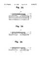
- FIG. 1is a sectional view of an ink spraying device for a print head according to the present invention
- FIGS. 2-14are cross-sectional side views showing the process, in sequence, for forming the ink heating portion of the device shown in FIG. 1;
- FIGS. 15-26are cross-sectional side views showing the process, in sequence, for forming the ink spraying portion of the device shown in FIG. 1.
- An embodiment of the ink spraying device of a print head of the present inventionlargely comprises: an ink heating portion (see FIG. 14) for generating thermal energy when electric energy is applied and thereby heating a heating fluid; and an ink spraying portion (see FIG. 26), assembled onto the ink heating portion in alignment therewith, for ejecting temporarily stored ink in accordance with the generated thermal energy.
- the ink heating portionincludes a substrate 11, a protective layer 12 for protecting the surface of the substrate 11, a heating layer 13 selectively formed on the protective layer 12 for generating heat in accordance with an applied electric energy, a pair of electrodes 14a and 14b in contact with the heating layer 13 in order to supply electric energy thereto, first and second passivation layers 15 and 16 for protecting the interior from being damaged by the generated heat, an electrical contact 19 for providing external selective connection to one electrode (the other electrode being part of the common electrode), and a heating chamber barrier 17 defining a heating chamber 18.
- the ink spraying portionincludes a nozzle plate 21 having an opening 21a through which ink droplets are ejected, an ink chamber barrier 22 defining an ink chamber 23, and a plurality of membranes 24 formed over the ink chamber barrier 22 for receiving the thermal energy produced by the ink heating portion in order to form and eject the ink droplets. It should be appreciated that such a structure forms a unified subassembly incorporating both the heating chamber and nozzle plate, which are preformed using photolithographic techniques such that their relative positioning is fixed without any step for manual alignment.
- silicon dioxideSiO 2
- a resistive material 13' used to form the heating layer 13is deposited on the protective layer 12, and a conductive material used to form the electrode layer 14 is deposited on the heating layer.
- the electrode layer 14is made up of an aluminum sputtering deposition atop a tantalum-aluminum alloy layer formed to a predetermined thickness, the result of which is then patterned.
- a photoresist material 30is coated on the electrode layer 14 followed by a planarization step, and then a first mask 41 for forming the electrode pattern is laid on the planarized photoresist. With the first mask 41 in place, the photoresist material 30 is exposed to ultraviolet light to react therewith.
- a positive photoresistis used so that the developed photoresist is removed, creating a first photoresist pattern 31 as shown in FIG. 3, and the electrode layer 14 is then dry-etched into electrodes 14a and 14b as, shown in FIG. 4.
- the photoresist material 30is coated on the patterned electrode layer, and a second mask 42 for forming the heating layer pattern is attached to the planarized surface thereof, as shown in FIG. 5.
- the heating layer 13is formed through an exposure and development process, similar to that described above, followed by a further etching step.
- a layer 15' of silicon nitride (Si 3 N 4 ), silicon carbide (SiC) or tantalumis used to form the first passivation layer 15, as shown in FIG. 7.
- a chemical vapor deposition processmay be used.
- photoresist material 30is again coated and planarized and a third mask 43 is placed. thereon as shown in FIG. 8.
- the subsequent exposure and development processproduces a photoresist pattern 33 for etching the first passivation layer to form, a contact via therein.
- the third mask 43is replaced and gold, i.e., a highly conductive material, is used to form the electrical contact 19, as shown in FIG. 10.
- a tantalum layer 16'is deposited on the resulting structure.
- a patterning process similar to that described above, using a planarized surface of the photoresist material 30 and a fourth mask 44 as shown in FIG. 11,is used to form, the second passivation layer 16 and thereby expose the electrical contact 19 as shown in FIG. 12.
- the formation of the heating chamber 18is accomplished through the deposition of a photopolymer layer 17' on the passivation layers 15 and 16, to a thickness determinant of the chamber's size. As shown in FIG. 13, a fifth mask 45 having the pattern of the heating chamber barrier 17 is placed atop the planarized photopolymer surface which has photosensitive properties like the photoresist. Thus, by exposure to ultraviolet light and a corresponding etching process, the heating chamber barrier 17 is formed, as shown in FIG. 14, to thereby define the heating chamber 18. This completes the manufacturing process of the ink heating portion.
- an oxide layer 28is formed on a polished substrate 29 and a photoresist material 30 is coated thereon.
- a photoresist pattern 36is formed as shown in FIG. 16.
- An electroplating processis then performed using the material of the nozzle plate 21, e.g., nickel, as shown in FIG. 17, and the pattern 36 is removed to create an opening 21 a, i.e., nozzle, as shown in FIG. 18.
- a seventh mask 47having the pattern of the ink chamber barrier 22 laid atop a planarized surface of the photoresist 30 as shown in FIG. 19, a photoresist pattern 37 is formed and, using the same mask again as shown in FIG. 20, a polyamide deposition is performed to give the structure of FIG. 21 showing the ink chamber barrier 22 defining the ink chamber 23.
- An eighth mask 48 having the pattern of the interior of the ink chamber 23is placed atop the ink chamber barrier 22 and coated with photoresist material 38 so to form a support mechanism for the subsequent processing, as shown in FIG. 22.
- photoresist material 38is employed due to its relative ease of removal.
- a plurality of membrane layers 24'are individually applied, as in FIG. 23, and patterned to form a plurality of membranes 24, as in FIG. 24, using the same mask (not shown) for each layer one of the plurality of membranes of the membrane layer forming an enclosing surface of the heating chamber and another of the plurality of membranes of the membrane layer forming an enclosing surface of the ink chamber, as illustrated in FIG. 1, for example.
- the material of each membrane layer or membranehas a different coefficient of thermal expansion.
- the substrate layers 28 and 29, having performed their purpose,are lifted off as in FIG. 25 and the membrane support mechanism of photoresist material 38 is removed as in FIG. 26.
- the layer in contact with the nozzle plate 21can be easily detached therefrom since nickel is weak in adhesion. This completes the manufacture of the ink spraying portion.
- the separate manufacture of the ink heating portion and the ink spraying portionare concluded.
- a high-temperature, high-pressure bonding techniqueis used to join the heating chamber barrier 17 of the ink heating portion with the membranes 24 of the ink spraying portion, to create a seal over the heating chamber 18. This allows for assembly tolerances of up to several micrometers, since the alignment tolerance of the nozzle with the ink chamber is rendered moot.
Landscapes
- Engineering & Computer Science (AREA)
- Manufacturing & Machinery (AREA)
- Particle Formation And Scattering Control In Inkjet Printers (AREA)
Abstract
Description
Claims (22)
Applications Claiming Priority (2)
| Application Number | Priority Date | Filing Date | Title |
|---|---|---|---|
| KR97-959 | 1997-01-15 | ||
| KR1019970000959AKR100225082B1 (en) | 1997-01-15 | 1997-01-15 | Ink ejector structure of the print head |
Publications (1)
| Publication Number | Publication Date |
|---|---|
| US6126272Atrue US6126272A (en) | 2000-10-03 |
Family
ID=19494697
Family Applications (1)
| Application Number | Title | Priority Date | Filing Date |
|---|---|---|---|
| US09/007,821Expired - LifetimeUS6126272A (en) | 1997-01-15 | 1998-01-15 | Ink spraying device for print head |
Country Status (2)
| Country | Link |
|---|---|
| US (1) | US6126272A (en) |
| KR (1) | KR100225082B1 (en) |
Cited By (4)
| Publication number | Priority date | Publication date | Assignee | Title |
|---|---|---|---|---|
| US6257706B1 (en)* | 1997-10-15 | 2001-07-10 | Samsung Electronics Co., Ltd. | Micro injecting device and a method of manufacturing |
| EP1205303A1 (en)* | 2000-11-07 | 2002-05-15 | Sony Corporation | Printer, printer head, and method of producing the printer head |
| US20030025765A1 (en)* | 2000-07-25 | 2003-02-06 | Moon Jae-Ho | Ink jet printer head and fabrication method for an ink jet printer head |
| US20030098899A1 (en)* | 2001-11-29 | 2003-05-29 | Samsung Electronics Co., Ltd. | Ink-jet printhead and manufacturing method thereof |
Families Citing this family (3)
| Publication number | Priority date | Publication date | Assignee | Title |
|---|---|---|---|---|
| KR100620286B1 (en)* | 1999-11-04 | 2006-09-07 | 삼성전자주식회사 | Nozzle part manufacturing method of ink jetting device and ink jetting device |
| KR100672053B1 (en)* | 1999-11-04 | 2007-01-22 | 삼성전자주식회사 | Ink spraying device with heater spaced apart from membrane |
| KR100339358B1 (en)* | 2000-03-30 | 2002-06-03 | 구자홍 | Vibration absorbing structure of control part for refrigerator |
Citations (20)
| Publication number | Priority date | Publication date | Assignee | Title |
|---|---|---|---|---|
| US4353078A (en)* | 1979-09-24 | 1982-10-05 | International Business Machines Corporation | Ink jet print head having dynamic impedance adjustment |
| US4480259A (en)* | 1982-07-30 | 1984-10-30 | Hewlett-Packard Company | Ink jet printer with bubble driven flexible membrane |
| US4513298A (en)* | 1983-05-25 | 1985-04-23 | Hewlett-Packard Company | Thermal ink jet printhead |
| US4580148A (en)* | 1985-02-19 | 1986-04-01 | Xerox Corporation | Thermal ink jet printer with droplet ejection by bubble collapse |
| JPS6237163A (en)* | 1985-08-10 | 1987-02-18 | Toyoda Autom Loom Works Ltd | Droplet ejector |
| US4716423A (en)* | 1985-11-22 | 1987-12-29 | Hewlett-Packard Company | Barrier layer and orifice plate for thermal ink jet print head assembly and method of manufacture |
| JPH02111549A (en)* | 1988-10-20 | 1990-04-24 | Seiko Epson Corp | Printing equipment that uses hot melt ink |
| JPH02179748A (en)* | 1988-12-29 | 1990-07-12 | Matsushita Electric Ind Co Ltd | Ink recorder |
| US4942408A (en)* | 1989-04-24 | 1990-07-17 | Eastman Kodak Company | Bubble ink jet print head and cartridge construction and fabrication method |
| US5153610A (en)* | 1984-01-31 | 1992-10-06 | Canon Kabushiki Kaisha | Liquid jet recording head |
| JPH0687213A (en)* | 1992-09-04 | 1994-03-29 | Brother Ind Ltd | Ink-jet printer head |
| US5364743A (en)* | 1990-12-21 | 1994-11-15 | Xerox Corporation | Process for fabrication of bubble jet using positive resist image reversal for lift off of passivation layer |
| US5463411A (en)* | 1992-04-28 | 1995-10-31 | Eastman Kodak Company | Electrothermal ink print head |
| US5467112A (en)* | 1992-06-19 | 1995-11-14 | Hitachi Koki Co., Ltd. | Liquid droplet ejecting apparatus |
| US5515085A (en)* | 1991-10-17 | 1996-05-07 | Minolta Camera Kabushiki Kaisha | Ink-jet type recorder |
| JPH08118632A (en)* | 1994-10-19 | 1996-05-14 | Fujitsu Ltd | Inkjet head |
| US5539437A (en)* | 1994-01-10 | 1996-07-23 | Xerox Corporation | Hybrid thermal/hot melt ink jet print head |
| US5684519A (en)* | 1994-04-19 | 1997-11-04 | Sharp Kabushiki Kaisha | Ink jet head with buckling structure body |
| US5718044A (en)* | 1995-11-28 | 1998-02-17 | Hewlett-Packard Company | Assembly of printing devices using thermo-compressive welding |
| US5809646A (en)* | 1993-09-03 | 1998-09-22 | Microparts Gmbh | Method of making a nozzle plate for a liquid jet print head |
- 1997
- 1997-01-15KRKR1019970000959Apatent/KR100225082B1/ennot_activeExpired - Fee Related
- 1998
- 1998-01-15USUS09/007,821patent/US6126272A/ennot_activeExpired - Lifetime
Patent Citations (20)
| Publication number | Priority date | Publication date | Assignee | Title |
|---|---|---|---|---|
| US4353078A (en)* | 1979-09-24 | 1982-10-05 | International Business Machines Corporation | Ink jet print head having dynamic impedance adjustment |
| US4480259A (en)* | 1982-07-30 | 1984-10-30 | Hewlett-Packard Company | Ink jet printer with bubble driven flexible membrane |
| US4513298A (en)* | 1983-05-25 | 1985-04-23 | Hewlett-Packard Company | Thermal ink jet printhead |
| US5153610A (en)* | 1984-01-31 | 1992-10-06 | Canon Kabushiki Kaisha | Liquid jet recording head |
| US4580148A (en)* | 1985-02-19 | 1986-04-01 | Xerox Corporation | Thermal ink jet printer with droplet ejection by bubble collapse |
| JPS6237163A (en)* | 1985-08-10 | 1987-02-18 | Toyoda Autom Loom Works Ltd | Droplet ejector |
| US4716423A (en)* | 1985-11-22 | 1987-12-29 | Hewlett-Packard Company | Barrier layer and orifice plate for thermal ink jet print head assembly and method of manufacture |
| JPH02111549A (en)* | 1988-10-20 | 1990-04-24 | Seiko Epson Corp | Printing equipment that uses hot melt ink |
| JPH02179748A (en)* | 1988-12-29 | 1990-07-12 | Matsushita Electric Ind Co Ltd | Ink recorder |
| US4942408A (en)* | 1989-04-24 | 1990-07-17 | Eastman Kodak Company | Bubble ink jet print head and cartridge construction and fabrication method |
| US5364743A (en)* | 1990-12-21 | 1994-11-15 | Xerox Corporation | Process for fabrication of bubble jet using positive resist image reversal for lift off of passivation layer |
| US5515085A (en)* | 1991-10-17 | 1996-05-07 | Minolta Camera Kabushiki Kaisha | Ink-jet type recorder |
| US5463411A (en)* | 1992-04-28 | 1995-10-31 | Eastman Kodak Company | Electrothermal ink print head |
| US5467112A (en)* | 1992-06-19 | 1995-11-14 | Hitachi Koki Co., Ltd. | Liquid droplet ejecting apparatus |
| JPH0687213A (en)* | 1992-09-04 | 1994-03-29 | Brother Ind Ltd | Ink-jet printer head |
| US5809646A (en)* | 1993-09-03 | 1998-09-22 | Microparts Gmbh | Method of making a nozzle plate for a liquid jet print head |
| US5539437A (en)* | 1994-01-10 | 1996-07-23 | Xerox Corporation | Hybrid thermal/hot melt ink jet print head |
| US5684519A (en)* | 1994-04-19 | 1997-11-04 | Sharp Kabushiki Kaisha | Ink jet head with buckling structure body |
| JPH08118632A (en)* | 1994-10-19 | 1996-05-14 | Fujitsu Ltd | Inkjet head |
| US5718044A (en)* | 1995-11-28 | 1998-02-17 | Hewlett-Packard Company | Assembly of printing devices using thermo-compressive welding |
Cited By (8)
| Publication number | Priority date | Publication date | Assignee | Title |
|---|---|---|---|---|
| US6257706B1 (en)* | 1997-10-15 | 2001-07-10 | Samsung Electronics Co., Ltd. | Micro injecting device and a method of manufacturing |
| US20030025765A1 (en)* | 2000-07-25 | 2003-02-06 | Moon Jae-Ho | Ink jet printer head and fabrication method for an ink jet printer head |
| EP1205303A1 (en)* | 2000-11-07 | 2002-05-15 | Sony Corporation | Printer, printer head, and method of producing the printer head |
| US6685304B2 (en) | 2000-11-07 | 2004-02-03 | Sony Corporation | Printer, printer head and method of producing the print head to promote reliable bonding of print head structures |
| US20030098899A1 (en)* | 2001-11-29 | 2003-05-29 | Samsung Electronics Co., Ltd. | Ink-jet printhead and manufacturing method thereof |
| US7341332B2 (en)* | 2001-11-29 | 2008-03-11 | Samsung Electronics Co., Ltd. | Ink-jet printhead and manufacturing method thereof |
| US20080096296A1 (en)* | 2001-11-29 | 2008-04-24 | Samsung Electronics Co., Ltd. | Ink-jet printhead and manufacturing method thereof |
| US7758165B2 (en) | 2001-11-29 | 2010-07-20 | Samsung Electronics Co., Ltd. | Ink-jet printhead and manufacturing method thereof |
Also Published As
| Publication number | Publication date |
|---|---|
| KR100225082B1 (en) | 1999-10-15 |
| KR19980065807A (en) | 1998-10-15 |
Similar Documents
| Publication | Publication Date | Title |
|---|---|---|
| CA1302160C (en) | Integrated thermal ink jet printhead and method of manufacture | |
| JP3213624B2 (en) | Print head | |
| JP2716418B2 (en) | Manufacturing method of thermal ink jet print head | |
| US5194877A (en) | Process for manufacturing thermal ink jet printheads having metal substrates and printheads manufactured thereby | |
| EP0962320A1 (en) | Ink-Jet head, ink-jet head substrate, and a method for making the head | |
| JP2008087478A (en) | Ink jet print head and manufacturing method thereof | |
| KR100445004B1 (en) | Monolithic ink jet print head and manufacturing method thereof | |
| US6126272A (en) | Ink spraying device for print head | |
| US6846068B2 (en) | Monolithic ink-jet printhead and method for manufacturing the same | |
| US8388117B2 (en) | Method of making an inkjet printhead | |
| WO1997046390A1 (en) | Ink jet head and method of manufacturing same | |
| US8806752B2 (en) | Micro-fluid ejection device and method for assembling a micro-fluid ejection device by a wafer-to-wafer bonding | |
| US6811715B2 (en) | Method for producing ink jet recording head, and ink jet recording head produced by such method | |
| US6368515B1 (en) | Method of manufacturing ink-jet printer head | |
| TW580436B (en) | Ink-jet micro-injector device and fabrication method thereof | |
| GB2151555A (en) | Liquid jet recording head | |
| US7922922B2 (en) | Ink jet print head manufacturing method and ink jet print head | |
| US6315385B1 (en) | Self-locating orifice plate construction for thermal ink jet printheads | |
| US8152280B2 (en) | Method of making an inkjet printhead | |
| KR100190123B1 (en) | Method for manufacturing inkjet printer head having ink nozzle plate in a body | |
| JPH11245425A (en) | Manufacturing method of thermal inkjet head | |
| KR20030079199A (en) | Method for manufacturing monolithic inkjet printhead | |
| JPH08118633A (en) | Ink jet head | |
| JPH08187856A (en) | Ink jet recording head | |
| JP2002347254A (en) | How to make an ink jet recording head |
Legal Events
| Date | Code | Title | Description |
|---|---|---|---|
| AS | Assignment | Owner name:SAMSUNG ELECTRONICS CO., LTD., KOREA, REPUBLIC OF Free format text:ASSIGNMENT OF ASSIGNORS INTEREST;ASSIGNOR:AHN, BYUNG-SUN;REEL/FRAME:009125/0390 Effective date:19971110 | |
| STCF | Information on status: patent grant | Free format text:PATENTED CASE | |
| FEPP | Fee payment procedure | Free format text:PAYOR NUMBER ASSIGNED (ORIGINAL EVENT CODE: ASPN); ENTITY STATUS OF PATENT OWNER: LARGE ENTITY | |
| FPAY | Fee payment | Year of fee payment:4 | |
| FPAY | Fee payment | Year of fee payment:8 | |
| FEPP | Fee payment procedure | Free format text:PAYOR NUMBER ASSIGNED (ORIGINAL EVENT CODE: ASPN); ENTITY STATUS OF PATENT OWNER: LARGE ENTITY Free format text:PAYER NUMBER DE-ASSIGNED (ORIGINAL EVENT CODE: RMPN); ENTITY STATUS OF PATENT OWNER: LARGE ENTITY | |
| FPAY | Fee payment | Year of fee payment:12 | |
| AS | Assignment | Owner name:S-PRINTING SOLUTION CO., LTD., KOREA, REPUBLIC OF Free format text:ASSIGNMENT OF ASSIGNORS INTEREST;ASSIGNOR:SAMSUNG ELECTRONICS CO., LTD;REEL/FRAME:041852/0125 Effective date:20161104 | |
| AS | Assignment | Owner name:HP PRINTING KOREA CO., LTD., KOREA, REPUBLIC OF Free format text:CHANGE OF NAME;ASSIGNOR:S-PRINTING SOLUTION CO., LTD.;REEL/FRAME:047370/0405 Effective date:20180316 | |
| AS | Assignment | Owner name:HP PRINTING KOREA CO., LTD., KOREA, REPUBLIC OF Free format text:CORRECTIVE ASSIGNMENT TO CORRECT THE DOCUMENTATION EVIDENCING THE CHANGE OF NAME PREVIOUSLY RECORDED ON REEL 047370 FRAME 0405. ASSIGNOR(S) HEREBY CONFIRMS THE CHANGE OF NAME;ASSIGNOR:S-PRINTING SOLUTION CO., LTD.;REEL/FRAME:047769/0001 Effective date:20180316 | |
| AS | Assignment | Owner name:HP PRINTING KOREA CO., LTD., KOREA, REPUBLIC OF Free format text:CHANGE OF LEGAL ENTITY EFFECTIVE AUG. 31, 2018;ASSIGNOR:HP PRINTING KOREA CO., LTD.;REEL/FRAME:050938/0139 Effective date:20190611 | |
| AS | Assignment | Owner name:HEWLETT-PACKARD DEVELOPMENT COMPANY, L.P., TEXAS Free format text:CONFIRMATORY ASSIGNMENT EFFECTIVE NOVEMBER 1, 2018;ASSIGNOR:HP PRINTING KOREA CO., LTD.;REEL/FRAME:050747/0080 Effective date:20190826 |