US6125404A - Data processing system having a protocol timer for autonomously providing time based interrupts - Google Patents
Data processing system having a protocol timer for autonomously providing time based interruptsDownload PDFInfo
- Publication number
- US6125404A US6125404AUS09/061,958US6195898AUS6125404AUS 6125404 AUS6125404 AUS 6125404AUS 6195898 AUS6195898 AUS 6195898AUS 6125404 AUS6125404 AUS 6125404A
- Authority
- US
- United States
- Prior art keywords
- data processor
- processing system
- timer
- data processing
- events
- Prior art date
- Legal status (The legal status is an assumption and is not a legal conclusion. Google has not performed a legal analysis and makes no representation as to the accuracy of the status listed.)
- Expired - Lifetime
Links
Images


Classifications
- G—PHYSICS
- G06—COMPUTING OR CALCULATING; COUNTING
- G06F—ELECTRIC DIGITAL DATA PROCESSING
- G06F13/00—Interconnection of, or transfer of information or other signals between, memories, input/output devices or central processing units
- G06F13/14—Handling requests for interconnection or transfer
- G06F13/20—Handling requests for interconnection or transfer for access to input/output bus
- G06F13/24—Handling requests for interconnection or transfer for access to input/output bus using interrupt
- Y—GENERAL TAGGING OF NEW TECHNOLOGICAL DEVELOPMENTS; GENERAL TAGGING OF CROSS-SECTIONAL TECHNOLOGIES SPANNING OVER SEVERAL SECTIONS OF THE IPC; TECHNICAL SUBJECTS COVERED BY FORMER USPC CROSS-REFERENCE ART COLLECTIONS [XRACs] AND DIGESTS
- Y02—TECHNOLOGIES OR APPLICATIONS FOR MITIGATION OR ADAPTATION AGAINST CLIMATE CHANGE
- Y02D—CLIMATE CHANGE MITIGATION TECHNOLOGIES IN INFORMATION AND COMMUNICATION TECHNOLOGIES [ICT], I.E. INFORMATION AND COMMUNICATION TECHNOLOGIES AIMING AT THE REDUCTION OF THEIR OWN ENERGY USE
- Y02D10/00—Energy efficient computing, e.g. low power processors, power management or thermal management
Definitions
- the present inventionrelates in general to communications, and more particularly to a communication system having a protocol timer.
- Time division multiple access (TDMA) communication systemsshare a common transmission medium between a number of simultaneous users. Each user's transmission does not interfere with that of the other users because their transmissions are separated from each other in time.
- a requirement of an effective TDMA communications device, such as a cellular telephone,is that the device retain accurate time synchronization with respect to the other users.
- Base stations in a GSM cellular phone systemmay not be synchronized with each other.
- the handsetWhen a mobile handset moves from one base station's coverage area to another, the handset must be re-synchronized with the new base station's time base. The transition must be handled in a timely manner to prevent a loss of information.
- Prior art techniques for retaining accurate time synchronizationrely on a combination of software and hardware. These techniques suffer from timing errors and inhibit effective power management of the system. The timing errors result from errors introduced by software interaction with hardware, such as for example, interrupt latencies that delay software response to boundary conditions in the hardware. Also, uncertainties may be introduced when hardware counters are modified by software. Correcting these errors requires increased software complexity. In addition, power consumption may be higher than desirable because the system's central processing unit (CPU) must remain in an active state to execute the software component of the timing.
- Prior art techniquesovercome these issues in hardware but require relatively large surface area on an integrated circuit to implement.
- FIG. 1illustrates, in block diagram form, a communications system having a protocol timer in accordance with the present invention.
- FIG. 2illustrates, in block diagram form, protocol timer of the communication system of FIG. 1 in more detail.
- FIG. 3illustrates, in block diagram form, the frame event table of FIG. 2 in more detail.
- FIG. 4illustrates, in block diagram form, the macro event table of FIG. 2 in more detail.
- the present inventionprovides a communications system that includes multiple data processors and a protocol timer.
- the protocol timercontrols the timing of events in the communications system and operates autonomously after it is loaded with initial instructions.
- the protocol timercan provide multiple vectored interrupts to the multiple data processors. By allowing the protocol timer to operate autonomously, the other processors can be powered down when not in use, thus reducing power consumption of the communications system. Also, by using the protocol timer to control the timing of events, the number of software related errors are reduced.
- buswill be used to refer to a plurality of signals or conductors which may be used to transfer one or more various types of information, such as data, addresses, control, or status.
- pinis used throughout this document, this term is intended to encompass any type of apparatus which allows electrical signals to be transferred to or from an integrated circuit, such as, for example, integrated circuit bonding pads, solder bumps, wire conductors, etc.
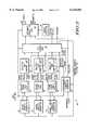
- FIG. 1illustrates, in block diagram form, a communications system having multiple processors and a protocol timer 18 in accordance with the present invention.
- the communications systemincludes transceiver 10, serial interface 32, serial interface 34, audio codec 36, speaker 38, and multi-processor data processing system 12.
- Data processing system 12includes data processor 14, data processor 16, protocol timer 18, memory 20, inter-processor communication unit 22, memory 24, bus interface 26, peripheral unit 28, and queued serial peripheral interface (QSPI) 30.
- QSPIqueued serial peripheral interface
- transceiver 10, serial interfaces 32 and 34, audio codec 36, and speaker/microphone 38form a "front end" for the communication system illustrated in FIG. 1.
- Peripheral unit 28may be one of many types of peripheral units, and may include additional memory, serial and/or parallel interface units, digital-to-analog converters, and the like.
- Transceiver 10is bi-directionally coupled to a transmission path 11 for receiving and/or providing data organized in frames. Data received from transmission path 11 is provided to serial interface 32. Serial interface 32 and serial interface 34 are bi-directionally coupled to processor 14. Note that in the illustrated embodiment processor 14 is a digital signal processor (DSP) and processor 16 is a microprocessor (MPU). Processor 14 is bi-directionally coupled to memory 20. Memory 20 can be any type of volatile or nonvolatile random access memory. Serial interface 34 is also bi-directionally coupled to an audio codec 36. Audio codec 36 receives and delivers audio information from and to speaker/microphone 38. Audio codec 36 converts the received audio information to a digital format, and provides the digital audio information to serial interface 34.
- DSPdigital signal processor
- MPUmicroprocessor
- Processor 16is bi-directionally coupled to memory 24 and to bus interface 26.
- Bus interface 26, peripheral unit 28 and QSPI 30are all coupled to the MPU bus.
- protocol timer 18, and processors 14 and 16are implemented on the same integrated circuit. However, in other embodiments, more than one integrated circuit may be used.
- Protocol timer 18has a first plurality of output terminals for providing interrupts, labeled “DSP INTERRUPTS", to an interrupt input of data processor 14, a second plurality of output terminals for providing interrupts, labeled “MPU INTERRUPTS”, to an interrupt input of data processor 16, a third plurality of output terminals for providing control signals, labeled “TRIGGERS”, to QSPI 30, and a fourth plurality of output terminals for providing control signals, labeled "CONTROL OUTPUTS", to transceiver 10. Also, protocol timer 18 is bi-directionally coupled to processor 16 via a read/write bus labeled "MPU R/W BUS" and bus interface 26.
- Inter-processor communication unit 22has a first plurality of output terminals for providing interrupts, labeled "VECTORED INTERRUPTS", to processor 14, and a second plurality of output terminals for providing interrupts, labeled "INTERRUPTS", to processor 16. Also, inter-processor communication unit 22 is coupled to processor 14 for providing a reset signal, labeled "RESET”, for resetting processor 14. In addition, inter-processor communication unit 22 is bi-directionally coupled to bus interface 26, memory 20, and processor 14. Inter-processor communication unit 22 coordinates communications between processor 14 and processor 16, and with any other processors that may be included in data processing system 12. A portion of memory 20 is used as message storage space for inter-processor communication unit 22.
- transceiver 10receives a bit stream, comprising a plurality of serial bits, from transmission path 11.
- the plurality of bitsare organized into frames of bits and comply with a particular signaling protocol, such as for example, the Global System for Mobile (GSM) communications standard which has been implemented in Europe.
- Serial interface 32receives the bit stream from transceiver 10 and converts the bit stream into a form that can be used by data processing system 12, and/or placed in memory 20.
- Processor 14receives the bit stream from serial interface 32.
- serial interface 32can provide the serial bit stream from memory 20 to transceiver 10 for transmission via transmission path 11.
- Serial interface 34serves as an interface between memory 20 and audio codec 36. Audio codec 36 interfaces digital interface 34 with speaker/microphone 38 and includes an analog-to-digital converter.
- serial interface 32may take various forms, and serial interfaces 34 and audio codec 36 may or may not be present.
- the communication system illustrated in FIG. 1is for use in a time division multiple access (TDMA) system such as GSM.
- TDMAtime division multiple access
- GSMtime division multiple access
- the present inventionis not limited to GSM and may be applied to any TDMA system, either wireline or wireless.
- Processor 14receives the bit stream serial interface 32, and performs low level processing on the bit stream in accordance with the applicable protocol. Also, processor 14 multiplexes and demultiplexes the payload and control information from the bit stream and provides the control information to processor 16 via inter-processor communication unit 22. Processor 14 transfers the payload information to and from serial interface 34 and audio codec 36. Processor 14 may also transfer the payload information to other input/output devices, as appropriate for the type of payload information, following further processing in accordance with the applicable protocol. The other input/output devices may be, for example, a data communications terminal or a fax machine. Memory 20 includes program and data storage space for use by processor 14.
- processor 16receives and sends control information to processor 14 via inter-processor communication unit 22.
- Memory 24stores program and data information for use by processor 16.
- the program information stored in memory 24is used by processor 16 to interpret the control information or data received from processor 14.
- the control information or dataare interpreted by processor 16 in accordance with a specific protocol, such as for example, GSM.
- Processor 16provides instructions to protocol timer 18 via bus interface 26 and the MPU R/W BUS.
- processor 16provides instructions to QSPI 30. Based on the instructions from processor 16, QSPI 30 provides control instructions to transceiver 10.
- protocol timer 18provides CONTROL OUTPUTS to transceiver 10 for controlling timing of the operation of transceiver 10.
- TRIGGERSmay also be provided to other peripherals, such as peripheral 28.
- protocol timer 18After instructions have been initially loaded into protocol timer 18 by processor 16, protocol timer 18 operates autonomously providing CONTROL OUTPUTS to transceiver 10, control signals TRIGGERS to QSPI 30, and interrupts to both processor 14 and processor 16. During operation, the events are alterable by processor 16. The interrupts cause the interrupted processor, either processor 14 or processor 16, to be interrupted from executing a current address to begin executing a selectable target address. Note that in the illustrated embodiment, processor 16 initially loads the instructions. However, in other embodiments, processor 14, or another processor, not shown, may load the instructions.
- protocol timer 18includes a plurality of stored event codes, and upon a match between a predetermined count value associated with an event, and a reference time value, protocol timer 18 causes a predetermined control function to occur.
- the event codecan cause any of: (1) one of processors 14 or 16 to receive an interrupt signal; (2) generation of a control signal for use in the communication system, such as in transceiver 10; (3) triggering of an event in a peripheral of the system; (4) control of flow of event recognition in protocol timer 18; or (5) controlling initiation of event recognition in the one or more comparators of protocol timer 18.
- the target address of an eventis selectable, based on the event code stored in protocol timer 18.
- Protocol timer 18relieves processor 16 of all communications system timing control duties, including the generation of the interrupts.
- Protocol timer 18generates timing information including the reference time value, and based on the timing information, provides the TRIGGERS to QSPI 30 and the CONTROL OUTPUTS to transceiver 10. The TRIGGERS cause QSPI 30 to transfer control bits to control the operation of transceiver 10. Also, based on the timing information generated by protocol timer 18, protocol timer 18 generates multiple vectored interrupts MPU INTERRUPTS to processor 14 and interrupts DSP INTERRUPTS to processor 16. Protocol timer 18 will be discussed later in connection with the discussion of FIG. 2.
- protocol timer 18By operating autonomously after being programmed, protocol timer 18 provides several advantages over prior art communication systems. For example, processors 14 and 16 are relieved of providing timer information and can then be used exclusively for their main processing tasks. Also, because processors 14 and 16 are not required to execute the software component of system timing, the processors can maximize the time they operate in a low power mode, thus reducing power consumption. In addition, many of the software based timing errors in the prior art are eliminated because protocol timer 18 does many of the timing functions once controlled by software executed on a CPU.
- FIG. 2illustrates, in block diagram form, protocol timer 18 of the communications system of FIG. 1.
- Protocol timer 18includes address generators 40, 42 and 44, macro event tables 46 and 48, frame event table 50, compare units 52, 54 and 56, pin control unit 58, interrupt generator 60, error detector 62, and programmable time base generator 64.
- MPU R/W BUSbi-directionally couples processor 16 of FIG. 1 to macro address generator 40, macro address generator 42, frame table address generator 44, macro event table 46 and 48, frame event table 50, programmable time base generator 64, pin control unit 58, and interrupt generation unit 60.
- event tables 46, 48 and 50are implemented in random access memory.
- Event table 46is addressed by address generator 40
- event table 48is addressed by address generator 42
- event table 50is addressed by address generator 44.
- the addressesare initially generated from the information received from the MPU R/W BUS and are incremented and updated by pin control unit 58.
- Pin control unit 58 and programmable timebase generator 64are coupled to address generators 40, 42 and 44 via a bus labeled "TIME BASE/ADDRESS CONTROL BUS".
- Programmable time base generator 64receives a clock signal, labeled "REFERENCE CLOCK”, and generates a signal labeled "ROLLOVER”, a count value labeled "ABSOLUTE REFERENCE VALUE” and a clock signal labeled "COUNT CLOCK".
- Relative time compare unit 52has a plurality of input terminals for receiving an offset value labeled "COUNT OFFSET VALUE" from macro event table 46, and a second plurality of input terminals for receiving the clock signal COUNT CLOCK from programmable time base generator 64. Relative time compare unit 52 counts consecutive COUNT CLOCK pulses until the COUNT OFFSET VALUE is reached. Relative time compare unit 52 then provides an output signal to pin control unit 58 indicating that pin control unit 58 is to receive an event code labeled "EVENT CODE" from event table 46. Note that event table 46 is illustrated in more detail in FIG. 4.
- Relative time compare unit 54has a first plurality of input terminals for receiving an offset value labeled "COUNT OFFSET VALUE" from macro event table 48, and a second plurality of input terminals for receiving the clock signal COUNT CLOCK. Relative time compare unit 54 counts consecutive COUNT CLOCK pulses until the COUNT OFFSET VALUE is reached. Relative time compare unit 54 then provides an output signal to pin control unit 58 indicating that the EVENT CODE from event table 48 is to be loaded.
- Absolute time compare unit 56has a first plurality of input terminals for receiving an absolute count value labeled "ABSOLUTE COUNT VALUE" from frame event table 50, and a second plurality of input terminals for receiving count value ABSOLUTE REFERENCE VALUE from programmable time base generator 64. As the ABSOLUTE REFERENCE VALUE decreases, an output signal is provided by absolute time compare unit 56 when the ABSOLUTE COUNT VALUE from event table 50 is equal to the ABSOLUTE REFERENCE VALUE, indicating that the EVENT CODE from event table 50 is to be loaded into pin control unit 58.
- pin control unit 58Based on the value of the EVENT CODE, pin control unit 58 causes interrupt generation unit 60 to provide either DSP INTERRUPTS to processor 14 or MPU INTERRUPTS to processor 16, or pin control unit 58 may provide CONTROL OUTPUTS to transceiver 10, or TRIGGERS to QSPI 30. Protocol timer 18 may generate multiple interrupts to multiple CPUs. In addition to interrupts being generated in response to the compare unit outputs, interrupt generation unit 60 also receives control signals from error detector 62 and will generate appropriate interrupts based on the type of error detected. For example, if error detector 62 detects inconsistent programming and/or illegal states, an interrupt will be generated.
- Programmable time based generator 64includes a programmable down counter that counts from a predetermined value to zero. Upon reaching zero, the programmable down counter repeats counting from the predetermined value. For GSM applications the programmable counter is characterized as a modulo 5000 counter. Note that for use in other TDMA applications, such as for example, Asymmetrical Digital Subscriber Line (ADSL), the programmable time based modulo counter may be programmed for other count values.
- control signal ROLLOVERis provided to interrupt generation unit 60 and to pin control unit 50.
- pin control unit 50resets frame table address generator 44, and interrupt generation unit 60 may be programmed to provide an interrupt to processor 14 or processor 16.
- the pin control unit 58may, based upon the event code within frame event table 50, direct a "macro" event to be executed.
- a macrois a sequence of instructions for performing one or more communications operations in the communications system.
- a macro eventwill be executed from one of macro event table 46 or macro event table 48 under the control of macro address generator 40 or 42, respectively.
- Protocol timer 18can recognize a plurality of macro events occurring simultaneously, or in parallel, and can implement multiple control functions in the communications from the macro event tables. While protocol timer 18 is implementing control functions, one or both of processors 14 and 16 can be in a low power mode of operation.
- the interrupt signals VECTORED INTERRUPTS, that are provided to processor 16, and the interrupt signals INTERRUPTS, that are provided to processor 14,are generated by inter-processor communication unit 22 using event table information.
- the event table informationis provided to inter-processor communication unit 22 via the MPU R/W BUS.
- FIG. 3illustrates frame event table 50 in more detail.
- Frame event table 50includes a plurality of storage regions, or sections. Each section contains a number of entries.
- Frame event table 50includes two sections, labeled with "0" and "1" on the left side of the table. Both sections have substantially the same organization and are for storing a predetermined number of event operation codes. One of the sections is active while the other section is in standby.
- the inactive sectionmay be activated by protocol timer 18 dynamically switching to the inactive section in response to recognition of one or more predetermined events.
- Each frame entry, or eventincludes a bit field (14-bits) for storing an absolute count value, or time stamp, and a bit field (7-bits) for storing the event operation code. Frame events are implemented based on absolute time, and macro events are implemented based on relative time.
- the event codes stored within frame event table 50are for processing the frames of data in accordance with the applicable protocol, such as for example, GSM.
- GSMGlobal System for Mobile communications
- events necessary for processing dataare similar to each other, those events can be collected and stored as one macro event. For example, events for receive bursts of data and for adjacent cell power measurements are similar and can each be represented with one macro. By collecting events into macros, event tables can be smaller, thus requiring less memory space in the data processing system. Also, organizing a number of events as macros allows events and macros to be executed in parallel. The ability to execute events and macros in parallel may be important, for example, when it is necessary to begin preparing for a transmit operation before a receive operation has ended.
- some of the event operation codesrefer to macros, such that the macro directs pin control unit 58 to begin executing one of the macros stored in macro event tables 46 and/or 48.
- macro event table executionis based on programmable offsets rather than absolute count values from programmable time base generator 64.
- Each time a macro is listedan offset is required for macro event timing.
- the amount of offsetis programmable and is indicated in the Frame Event Table above by including a "delay" in parentheses following the event operation code.
- Macro event tables 46 and 48each include delay buffers for storing the programmable offset delays within the macro sequences.
- frame event table 50is also used to specify which delay buffer entry to use with a particular macro event.
- FIG. 4illustrates, in block diagram form, the macro event table 46 of FIG. 2 in more detail.
- macro event table 46includes a plurality of sections. Each section contains a number of entries. Macro event table 46 includes two sections, labeled with "0" and "1" on the left side of the table. Both sections have substantially the same organization and are for storing a predetermined number of macro operation codes.
- Each entry, or eventincludes a bit field (14-bits) for storing an relative count value, or time stamp, and a bit field (7-bits) for storing the event operation code.
- the delay buffersfor storing the programmable offset delay values. The offsets are based on the relative count value, and each macro can choose from multiple delays.
- the offset valuesare selectable, and can be used to change the sequence of events without changing the relative timing relationship of other subsequent events that are based on the same relative count value.
- the table belowincludes two examples of a macro, a receive (RX) macro and a transmit (TX) macro, as used above in the Frame Event Table of FIG. 3.
- event tables 46, 48 and 50allow parallel event execution. Therefore, the need for providing content addressable memory (as in some prior art systems) for parallel event execution is eliminated.
- the interruptsare programmable at precisely controlled intervals or points in time, which is important in real time processing applications.
- protocol timer 18may generate multiple interrupts to multiple CPUs.
- macro event tablesalso reduces the amount of storage area needed to store frame events, and the delay buffers allow a macro to be reused for similar operations at different times in the bit stream.
- macro event tablesallow an overlap of event timing sequences and the movement of those sequences relative to each other without requiring that the event table be sorted or reordered.
- the use of softwareis limited to pre-sorting of event entries by time stamping the event codes, and is thus, relatively easy to implement.
Landscapes
- Engineering & Computer Science (AREA)
- Theoretical Computer Science (AREA)
- Physics & Mathematics (AREA)
- General Engineering & Computer Science (AREA)
- General Physics & Mathematics (AREA)
- Power Sources (AREA)
Abstract
Description
______________________________________ Frame Event Table Absolute Count Value Event Operation Code Comments ______________________________________ 5000 MCU.sub.-- Int0 Prepare MCU for Burst RX 4900 DSP.sub.-- Int0 Prepare DSP for Burst RX 4800 RX.sub.-- Macro(burst.sub.-- rx.sub.-- delay) Do Burst Receive 4600 DSP.sub.-- Int8 DSP prepare TX Burst 4300 MCU.sub.-- Int1 Prepare MCU for Burst TX 4200 TX.sub.-- Macro(burst.sub.-- tx.sub.-- delay) Do Burst Transmit 4000 DSP.sub.-- Int1 RX Complete - Process Burst 3400 MCU.sub.-- Int2 Prepare MCU for Adjacent Cell RX 3350 DSP.sub.-- Int4 Prepare DSP for Adjacent Cell RX 3200 DSP.sub.-- Int9 TX Complete 3000 RX.sub.-- Macro(adjacent.sub.-- rx.sub.-- delay) Do Adjacent Cell Receive 2600 MCU.sub.-- Int2 Prepare MCU for Adjacent Cell RX 2500 DSP.sub.-- Int5 Adjacent Cell RX Complete - Process 2499 RX.sub.-- Macro(adjacent.sub.-- rx.sub.-- delay) Do Adjacent Cell Receive 2100 MCU.sub.-- Int2 Prepare MCU for Adjacent Cell RX 2000 DSP.sub.-- Int5 Adjacent Cell RX Complete - Process 1999 RX.sub.-- Macro(adjacent.sub.-- rx.sub.-- delay) Do Adjacent Cell Receive 1500 DSP.sub.-- int6 Last Adjacent Cell RX Complete - Process 1001 DSP.sub.-- int15 Enter Low power mode 1000 End.sub.-- of.sub.-- frame.sub.-- repeat Wait until counter rollover and repeat ______________________________________
______________________________________ Macro Event Table (RX Macro) Count Offset Value Event Operation Code Comments ______________________________________ +0Trigger QSFI Queue 0 Program synth/pll with RX frequency +10 Assert RX.sub.-- OSC.sub.-- On Turn on receive oscillator +180 Assert RX.sub.-- On Turn on receiver +10 Assert RX.sub.-- Enable Begin to receive samples +10 Delay Wait length of frame +1 Negate RX.sub.-- Enable Stop receiving samples +0 Negate RX.sub.-- On Turn off RX circuits +0 Negate RX.sub.-- OSC.sub.-- On +0 End.sub.-- of.sub.-- macro ______________________________________
______________________________________ Macro Event Table (TX Macro) Count Offset Value Event Operation Code Comments ______________________________________ +0Trigger QSPI Queue 1 Program synth/pll with TX frequency +10 Assert TX.sub.-- OSC.sub.-- On Turn on transmit oscillator +180 Assert PA.sub.-- On Turn on RF Power Amplifier +10 Assert TX.sub.-- On Turn on rest of transmitter +10 Assert TX.sub.-- Enable Begin to transmit samples +1 Delay Wait length of frame +0 Negate TX.sub.-- Enable Stop transmitting samples +0 Negate TX.sub.-- On Turn off TX circuits +0 Negate TX.sub.-- OSC.sub.-- On +0 Negate TX.sub.-- On +0 End.sub.-- of.sub.-- macro ______________________________________
Claims (21)
Priority Applications (1)
| Application Number | Priority Date | Filing Date | Title |
|---|---|---|---|
| US09/061,958US6125404A (en) | 1998-04-17 | 1998-04-17 | Data processing system having a protocol timer for autonomously providing time based interrupts |
Applications Claiming Priority (1)
| Application Number | Priority Date | Filing Date | Title |
|---|---|---|---|
| US09/061,958US6125404A (en) | 1998-04-17 | 1998-04-17 | Data processing system having a protocol timer for autonomously providing time based interrupts |
Publications (1)
| Publication Number | Publication Date |
|---|---|
| US6125404Atrue US6125404A (en) | 2000-09-26 |
Family
ID=22039297
Family Applications (1)
| Application Number | Title | Priority Date | Filing Date |
|---|---|---|---|
| US09/061,958Expired - LifetimeUS6125404A (en) | 1998-04-17 | 1998-04-17 | Data processing system having a protocol timer for autonomously providing time based interrupts |
Country Status (1)
| Country | Link |
|---|---|
| US (1) | US6125404A (en) |
Cited By (32)
| Publication number | Priority date | Publication date | Assignee | Title |
|---|---|---|---|---|
| US6314524B1 (en)* | 1999-03-18 | 2001-11-06 | Intervoice Limited Partnership | Repetitive interval timing |
| US20030002537A1 (en)* | 2001-06-27 | 2003-01-02 | Schaller Lane B. | Method and apparatus for controlling the timing of a communication device |
| US6718479B1 (en)* | 2000-09-08 | 2004-04-06 | International Business Machines Corporation | Method, system, program, and data structures for managing hierarchical timing wheels |
| US20050265507A1 (en)* | 2003-12-29 | 2005-12-01 | Charbel Khawand | Method and system for employing adaptive event codes |
| US7239581B2 (en) | 2004-08-24 | 2007-07-03 | Symantec Operating Corporation | Systems and methods for synchronizing the internal clocks of a plurality of processor modules |
| US7272666B2 (en) | 2003-09-23 | 2007-09-18 | Symantec Operating Corporation | Storage management device |
| US7287133B2 (en) | 2004-08-24 | 2007-10-23 | Symantec Operating Corporation | Systems and methods for providing a modification history for a location within a data store |
| US7296008B2 (en) | 2004-08-24 | 2007-11-13 | Symantec Operating Corporation | Generation and use of a time map for accessing a prior image of a storage device |
| US20070271571A1 (en)* | 2006-04-04 | 2007-11-22 | Tadeusz Jarosinski | Apparatus and methods for discriminating late software commands sent to hardware |
| US7307977B1 (en) | 2002-10-01 | 2007-12-11 | Comsys Communication & Signal Processing Ltd. | Information transfer and interrupt event scheduling scheme for a communications transceiver incorporating multiple processing elements |
| US20080028254A1 (en)* | 2006-07-26 | 2008-01-31 | International Business Machines Corporation | Directly obtaining by application programs information usable in determining clock accuracy |
| US7409587B2 (en) | 2004-08-24 | 2008-08-05 | Symantec Operating Corporation | Recovering from storage transaction failures using checkpoints |
| US20080201500A1 (en)* | 2007-02-20 | 2008-08-21 | Ati Technologies Ulc | Multiple interrupt handling method, devices and software |
| US20080282103A1 (en)* | 2007-05-09 | 2008-11-13 | Microsoft Corporation | Lightweight time change detection |
| US20090083570A1 (en)* | 2007-09-25 | 2009-03-26 | Canon Kabushiki Kaisha | Transmission apparatus that transmits data according to a protocol, and method for measuring time in the transmission apparatus |
| US7536583B2 (en) | 2005-10-14 | 2009-05-19 | Symantec Operating Corporation | Technique for timeline compression in a data store |
| US7577807B2 (en) | 2003-09-23 | 2009-08-18 | Symantec Operating Corporation | Methods and devices for restoring a portion of a data store |
| US20090245334A1 (en)* | 2008-03-28 | 2009-10-01 | Qualcomm Incorporated | Wall clock timer and system for generic modem |
| US20090248920A1 (en)* | 2008-03-26 | 2009-10-01 | Qualcomm Incorporated | Off-Line Task List Architecture |
| US20090245192A1 (en)* | 2008-03-26 | 2009-10-01 | Qualcomm Incorporated | Reconfigurable Wireless Modem Sub-Circuits To Implement Multiple Air Interface Standards |
| US7631120B2 (en) | 2004-08-24 | 2009-12-08 | Symantec Operating Corporation | Methods and apparatus for optimally selecting a storage buffer for the storage of data |
| US20100115308A1 (en)* | 2007-01-18 | 2010-05-06 | Panasonic Corporation | Communication device and power supply method |
| US7725760B2 (en) | 2003-09-23 | 2010-05-25 | Symantec Operating Corporation | Data storage system |
| US7730222B2 (en) | 2004-08-24 | 2010-06-01 | Symantec Operating System | Processing storage-related I/O requests using binary tree data structures |
| US7804852B1 (en) | 2003-01-24 | 2010-09-28 | Douglas Durham | Systems and methods for definition and use of a common time base in multi-protocol environments |
| US7827362B2 (en) | 2004-08-24 | 2010-11-02 | Symantec Corporation | Systems, apparatus, and methods for processing I/O requests |
| US7844690B1 (en) | 2003-01-24 | 2010-11-30 | Douglas Durham | Systems and methods for creation and use of a virtual protocol analyzer |
| US7904428B2 (en) | 2003-09-23 | 2011-03-08 | Symantec Corporation | Methods and apparatus for recording write requests directed to a data store |
| US7991748B2 (en) | 2003-09-23 | 2011-08-02 | Symantec Corporation | Virtual data store creation and use |
| US8005503B2 (en)* | 2002-12-18 | 2011-08-23 | Broadcom Corporation | Synchronization of multiple processors in a multi-mode wireless communication device |
| US20130117504A1 (en)* | 2011-11-08 | 2013-05-09 | Xilinx, Inc. | Embedded memory and dedicated processor structure within an integrated circuit |
| US9680720B1 (en)* | 2010-03-23 | 2017-06-13 | Marvell Israel (M.I.S.L.) Ltd. | Operations, administration, and maintenance (OAM) engine |
Citations (10)
| Publication number | Priority date | Publication date | Assignee | Title |
|---|---|---|---|---|
| US4758945A (en)* | 1979-08-09 | 1988-07-19 | Motorola, Inc. | Method for reducing power consumed by a static microprocessor |
| US5053943A (en)* | 1984-01-30 | 1991-10-01 | Nec Corporation | Control circuit for autonomous counters of a plurality of cpu's or the like with intermittent operation and reset after a predetermined count |
| US5072444A (en)* | 1989-10-23 | 1991-12-10 | Motorola, Inc. | Central controller with adaptive message handling characteristics |
| US5204957A (en)* | 1988-08-19 | 1993-04-20 | Motorola | Integrated circuit timer with multiple channels and dedicated service processor |
| US5577237A (en)* | 1995-01-23 | 1996-11-19 | Tandem Computers, Incorporated | Protocol timer and method of using same |
| US5606714A (en)* | 1991-12-06 | 1997-02-25 | National Semiconductor Corporation | Integrated data processing system including CPU core and parallel, independently operating DSP module and having multiple operating modes |
| US5638054A (en)* | 1980-10-01 | 1997-06-10 | Motorola, Inc. | Paging receiver with modifiable features or functions |
| US5640538A (en)* | 1994-08-22 | 1997-06-17 | Adaptec, Inc. | Programmable timing mark sequencer for a disk drive |
| US5910944A (en)* | 1997-02-28 | 1999-06-08 | Motorola, Inc. | Radio telephone and method for operating a radiotelephone in slotted paging mode |
| US5917854A (en)* | 1994-11-14 | 1999-06-29 | Research In Motion Limited | Wireless radio modem with minimal interdevice RF interference |
- 1998
- 1998-04-17USUS09/061,958patent/US6125404A/ennot_activeExpired - Lifetime
Patent Citations (10)
| Publication number | Priority date | Publication date | Assignee | Title |
|---|---|---|---|---|
| US4758945A (en)* | 1979-08-09 | 1988-07-19 | Motorola, Inc. | Method for reducing power consumed by a static microprocessor |
| US5638054A (en)* | 1980-10-01 | 1997-06-10 | Motorola, Inc. | Paging receiver with modifiable features or functions |
| US5053943A (en)* | 1984-01-30 | 1991-10-01 | Nec Corporation | Control circuit for autonomous counters of a plurality of cpu's or the like with intermittent operation and reset after a predetermined count |
| US5204957A (en)* | 1988-08-19 | 1993-04-20 | Motorola | Integrated circuit timer with multiple channels and dedicated service processor |
| US5072444A (en)* | 1989-10-23 | 1991-12-10 | Motorola, Inc. | Central controller with adaptive message handling characteristics |
| US5606714A (en)* | 1991-12-06 | 1997-02-25 | National Semiconductor Corporation | Integrated data processing system including CPU core and parallel, independently operating DSP module and having multiple operating modes |
| US5640538A (en)* | 1994-08-22 | 1997-06-17 | Adaptec, Inc. | Programmable timing mark sequencer for a disk drive |
| US5917854A (en)* | 1994-11-14 | 1999-06-29 | Research In Motion Limited | Wireless radio modem with minimal interdevice RF interference |
| US5577237A (en)* | 1995-01-23 | 1996-11-19 | Tandem Computers, Incorporated | Protocol timer and method of using same |
| US5910944A (en)* | 1997-02-28 | 1999-06-08 | Motorola, Inc. | Radio telephone and method for operating a radiotelephone in slotted paging mode |
Non-Patent Citations (4)
| Title |
|---|
| Intel Microcontroller Handbook, "16-Bit Microcontroller," pp. 15-37 to 15-39, (1983). |
| Intel Microcontroller Handbook, 16 Bit Microcontroller, pp. 15 37 to 15 39, (1983).* |
| TPU Time Processor Unit Reference Manual, Section 1 Overview, pp. 1 1 to 1 6, (1990).* |
| TPU Time Processor Unit Reference Manual, Section 1 Overview, pp. 1-1 to 1-6, (1990). |
Cited By (55)
| Publication number | Priority date | Publication date | Assignee | Title |
|---|---|---|---|---|
| US6314524B1 (en)* | 1999-03-18 | 2001-11-06 | Intervoice Limited Partnership | Repetitive interval timing |
| US6718479B1 (en)* | 2000-09-08 | 2004-04-06 | International Business Machines Corporation | Method, system, program, and data structures for managing hierarchical timing wheels |
| US20030002537A1 (en)* | 2001-06-27 | 2003-01-02 | Schaller Lane B. | Method and apparatus for controlling the timing of a communication device |
| US7324558B2 (en)* | 2001-06-27 | 2008-01-29 | Freescale Semiconductor, Inc. | Method and apparatus for controlling the timing of a communication device |
| US7042909B2 (en)* | 2001-06-27 | 2006-05-09 | Freescale Semiconductor, Inc. | Method and apparatus for controlling the timing of a communication device |
| US20060285554A1 (en)* | 2001-06-27 | 2006-12-21 | Freescale Semiconductor, Inc. | Method and apparatus for controlling the timing of a communication device |
| US7307977B1 (en) | 2002-10-01 | 2007-12-11 | Comsys Communication & Signal Processing Ltd. | Information transfer and interrupt event scheduling scheme for a communications transceiver incorporating multiple processing elements |
| US8532701B2 (en) | 2002-12-18 | 2013-09-10 | Broadcom Corporation | Synchronization of multiple processors in a multi-mode wireless communication device |
| US8005503B2 (en)* | 2002-12-18 | 2011-08-23 | Broadcom Corporation | Synchronization of multiple processors in a multi-mode wireless communication device |
| US7804852B1 (en) | 2003-01-24 | 2010-09-28 | Douglas Durham | Systems and methods for definition and use of a common time base in multi-protocol environments |
| US7844690B1 (en) | 2003-01-24 | 2010-11-30 | Douglas Durham | Systems and methods for creation and use of a virtual protocol analyzer |
| US7954109B1 (en)* | 2003-01-24 | 2011-05-31 | Jds Uniphase Corporation | Systems and methods for time based sorting and display of captured data events in a multi-protocol communications system |
| US7725667B2 (en) | 2003-09-23 | 2010-05-25 | Symantec Operating Corporation | Method for identifying the time at which data was written to a data store |
| US7725760B2 (en) | 2003-09-23 | 2010-05-25 | Symantec Operating Corporation | Data storage system |
| US7584337B2 (en) | 2003-09-23 | 2009-09-01 | Symantec Operating Corporation | Method and system for obtaining data stored in a data store |
| US7991748B2 (en) | 2003-09-23 | 2011-08-02 | Symantec Corporation | Virtual data store creation and use |
| US7272666B2 (en) | 2003-09-23 | 2007-09-18 | Symantec Operating Corporation | Storage management device |
| US7904428B2 (en) | 2003-09-23 | 2011-03-08 | Symantec Corporation | Methods and apparatus for recording write requests directed to a data store |
| US7577807B2 (en) | 2003-09-23 | 2009-08-18 | Symantec Operating Corporation | Methods and devices for restoring a portion of a data store |
| US7577806B2 (en) | 2003-09-23 | 2009-08-18 | Symantec Operating Corporation | Systems and methods for time dependent data storage and recovery |
| US20050265507A1 (en)* | 2003-12-29 | 2005-12-01 | Charbel Khawand | Method and system for employing adaptive event codes |
| US7773714B2 (en)* | 2003-12-29 | 2010-08-10 | Motorola, Inc. | Method and system for employing adaptive event codes |
| US8521973B2 (en) | 2004-08-24 | 2013-08-27 | Symantec Operating Corporation | Systems and methods for providing a modification history for a location within a data store |
| US7409587B2 (en) | 2004-08-24 | 2008-08-05 | Symantec Operating Corporation | Recovering from storage transaction failures using checkpoints |
| US7827362B2 (en) | 2004-08-24 | 2010-11-02 | Symantec Corporation | Systems, apparatus, and methods for processing I/O requests |
| US7296008B2 (en) | 2004-08-24 | 2007-11-13 | Symantec Operating Corporation | Generation and use of a time map for accessing a prior image of a storage device |
| US7287133B2 (en) | 2004-08-24 | 2007-10-23 | Symantec Operating Corporation | Systems and methods for providing a modification history for a location within a data store |
| US7730222B2 (en) | 2004-08-24 | 2010-06-01 | Symantec Operating System | Processing storage-related I/O requests using binary tree data structures |
| US7631120B2 (en) | 2004-08-24 | 2009-12-08 | Symantec Operating Corporation | Methods and apparatus for optimally selecting a storage buffer for the storage of data |
| US7239581B2 (en) | 2004-08-24 | 2007-07-03 | Symantec Operating Corporation | Systems and methods for synchronizing the internal clocks of a plurality of processor modules |
| US7536583B2 (en) | 2005-10-14 | 2009-05-19 | Symantec Operating Corporation | Technique for timeline compression in a data store |
| WO2007115334A3 (en)* | 2006-04-04 | 2007-12-21 | Qualcomm Inc | Apparatus and methods for discriminating late software commands sent to hardware |
| US7661009B2 (en) | 2006-04-04 | 2010-02-09 | Qualcomm Incorporated | Apparatus and methods for discriminating late software commands sent to hardware |
| US20070271571A1 (en)* | 2006-04-04 | 2007-11-22 | Tadeusz Jarosinski | Apparatus and methods for discriminating late software commands sent to hardware |
| US20080229138A1 (en)* | 2006-07-26 | 2008-09-18 | International Business Machines Corporation | Directly obtaining by application programs information usable in determining clock accuracy |
| US20080028254A1 (en)* | 2006-07-26 | 2008-01-31 | International Business Machines Corporation | Directly obtaining by application programs information usable in determining clock accuracy |
| US7395448B2 (en) | 2006-07-26 | 2008-07-01 | International Business Machines Corporation | Directly obtaining by application programs information usable in determining clock accuracy |
| US8171313B2 (en)* | 2007-01-18 | 2012-05-01 | Panasonic Corporation | Communication device and power supply method |
| US20100115308A1 (en)* | 2007-01-18 | 2010-05-06 | Panasonic Corporation | Communication device and power supply method |
| US7953906B2 (en)* | 2007-02-20 | 2011-05-31 | Ati Technologies Ulc | Multiple interrupt handling method, devices and software |
| US20080201500A1 (en)* | 2007-02-20 | 2008-08-21 | Ati Technologies Ulc | Multiple interrupt handling method, devices and software |
| US20080282103A1 (en)* | 2007-05-09 | 2008-11-13 | Microsoft Corporation | Lightweight time change detection |
| US8219845B2 (en)* | 2007-05-09 | 2012-07-10 | Microsoft Corporation | Timer service uses a single timer function to perform timing services for both relative and absolute timers |
| US20090083570A1 (en)* | 2007-09-25 | 2009-03-26 | Canon Kabushiki Kaisha | Transmission apparatus that transmits data according to a protocol, and method for measuring time in the transmission apparatus |
| US8341453B2 (en)* | 2007-09-25 | 2012-12-25 | Canon Kabushiki Kaisha | Transmission apparatus that transmits data according to a protocol, and method for measuring time in the transmission apparatus |
| US20090248920A1 (en)* | 2008-03-26 | 2009-10-01 | Qualcomm Incorporated | Off-Line Task List Architecture |
| US20090245192A1 (en)* | 2008-03-26 | 2009-10-01 | Qualcomm Incorporated | Reconfigurable Wireless Modem Sub-Circuits To Implement Multiple Air Interface Standards |
| US8520571B2 (en) | 2008-03-26 | 2013-08-27 | Qualcomm Incorporated | Reconfigurable wireless modem sub-circuits to implement multiple air interface standards |
| US8458380B2 (en) | 2008-03-26 | 2013-06-04 | Qualcomm Incorporated | Off-line task list architecture utilizing tightly coupled memory system |
| US20090245334A1 (en)* | 2008-03-28 | 2009-10-01 | Qualcomm Incorporated | Wall clock timer and system for generic modem |
| WO2009120473A1 (en)* | 2008-03-28 | 2009-10-01 | Qualcomm Incorporated | Wall clock timer and system for generic modem control |
| US8787433B2 (en) | 2008-03-28 | 2014-07-22 | Qualcomm Incorporated | Wall clock timer and system for generic modem |
| US9680720B1 (en)* | 2010-03-23 | 2017-06-13 | Marvell Israel (M.I.S.L.) Ltd. | Operations, administration, and maintenance (OAM) engine |
| US20130117504A1 (en)* | 2011-11-08 | 2013-05-09 | Xilinx, Inc. | Embedded memory and dedicated processor structure within an integrated circuit |
| US8874837B2 (en)* | 2011-11-08 | 2014-10-28 | Xilinx, Inc. | Embedded memory and dedicated processor structure within an integrated circuit |
Similar Documents
| Publication | Publication Date | Title |
|---|---|---|
| US6125404A (en) | Data processing system having a protocol timer for autonomously providing time based interrupts | |
| US6560215B1 (en) | Method and apparatus for updating a timing offset in a communication device | |
| US11314567B2 (en) | Methods and apparatus for scheduling time sensitive operations among independent processors | |
| US6683886B1 (en) | Bluetooth communication units, wireless communication systems, wireless communication devices, bluetooth communications methods, and wireless communication methods | |
| US10862526B2 (en) | Modem and RF chips, application processor including the same and operating method thereof | |
| US9219540B2 (en) | Method and system for phase compensation in multi-path communication device | |
| EP1591906A1 (en) | Efficient data transfer from an ASIC to a host using DMA | |
| US10572410B2 (en) | Function-specific communication on a multi-drop bus for coexistence management | |
| US20030021262A1 (en) | Bluetooth baseband controller | |
| TWI427987B (en) | Communication apparatus and method and mobile telephone | |
| JP5002783B2 (en) | Communication device including dual timer unit | |
| US7289477B2 (en) | Communication apparatus including a buffer circuit having first and second portions for alternately storing results | |
| US8019382B2 (en) | Communication apparatus having a standard serial communication interface compatible with radio isolation | |
| KR100266923B1 (en) | Generating real-time events in a tdma digital wireless communication system | |
| US7433393B2 (en) | Apparatus for controlling a digital signal processor for radio isolation and associated methods | |
| KR100756091B1 (en) | Terminals of digital cordless communication systems, control units for terminals of such systems and methods for such control units | |
| US20050008095A1 (en) | Apparatus using interrupts for controlling a processor for radio isolation and associated methods | |
| US20100216506A1 (en) | System and Methods for Supporting Multiple Communications Protocols on a Mobile Phone Device | |
| JP5007382B2 (en) | Communication device having SIM interface compatible with wireless separation | |
| US7761056B2 (en) | Method of controlling a processor for radio isolation using a timer | |
| US8472990B2 (en) | Apparatus using interrupts for controlling a processor for radio isolation and associated method | |
| EP2068250B1 (en) | Method and apparatuses for communicating a message received from a main processor to a peripheral device |
Legal Events
| Date | Code | Title | Description |
|---|---|---|---|
| AS | Assignment | Owner name:MOTOROLA, INC., ILLINOIS Free format text:ASSIGNMENT OF ASSIGNORS INTEREST;ASSIGNORS:VAGLICA, JOHN J.;MCALINDEN, PAUL;NORMAN, ODED;AND OTHERS;REEL/FRAME:009354/0311;SIGNING DATES FROM 19980615 TO 19980714 | |
| STCF | Information on status: patent grant | Free format text:PATENTED CASE | |
| FPAY | Fee payment | Year of fee payment:4 | |
| AS | Assignment | Owner name:FREESCALE SEMICONDUCTOR, INC., TEXAS Free format text:ASSIGNMENT OF ASSIGNORS INTEREST;ASSIGNOR:MOTOROLA, INC.;REEL/FRAME:015698/0657 Effective date:20040404 Owner name:FREESCALE SEMICONDUCTOR, INC.,TEXAS Free format text:ASSIGNMENT OF ASSIGNORS INTEREST;ASSIGNOR:MOTOROLA, INC.;REEL/FRAME:015698/0657 Effective date:20040404 | |
| AS | Assignment | Owner name:CITIBANK, N.A. AS COLLATERAL AGENT, NEW YORK Free format text:SECURITY AGREEMENT;ASSIGNORS:FREESCALE SEMICONDUCTOR, INC.;FREESCALE ACQUISITION CORPORATION;FREESCALE ACQUISITION HOLDINGS CORP.;AND OTHERS;REEL/FRAME:018855/0129 Effective date:20061201 Owner name:CITIBANK, N.A. AS COLLATERAL AGENT,NEW YORK Free format text:SECURITY AGREEMENT;ASSIGNORS:FREESCALE SEMICONDUCTOR, INC.;FREESCALE ACQUISITION CORPORATION;FREESCALE ACQUISITION HOLDINGS CORP.;AND OTHERS;REEL/FRAME:018855/0129 Effective date:20061201 | |
| FPAY | Fee payment | Year of fee payment:8 | |
| AS | Assignment | Owner name:CITIBANK, N.A., AS COLLATERAL AGENT,NEW YORK Free format text:SECURITY AGREEMENT;ASSIGNOR:FREESCALE SEMICONDUCTOR, INC.;REEL/FRAME:024397/0001 Effective date:20100413 Owner name:CITIBANK, N.A., AS COLLATERAL AGENT, NEW YORK Free format text:SECURITY AGREEMENT;ASSIGNOR:FREESCALE SEMICONDUCTOR, INC.;REEL/FRAME:024397/0001 Effective date:20100413 | |
| FPAY | Fee payment | Year of fee payment:12 | |
| AS | Assignment | Owner name:CITIBANK, N.A., AS NOTES COLLATERAL AGENT, NEW YORK Free format text:SECURITY AGREEMENT;ASSIGNOR:FREESCALE SEMICONDUCTOR, INC.;REEL/FRAME:030633/0424 Effective date:20130521 Owner name:CITIBANK, N.A., AS NOTES COLLATERAL AGENT, NEW YOR Free format text:SECURITY AGREEMENT;ASSIGNOR:FREESCALE SEMICONDUCTOR, INC.;REEL/FRAME:030633/0424 Effective date:20130521 | |
| AS | Assignment | Owner name:CITIBANK, N.A., AS NOTES COLLATERAL AGENT, NEW YORK Free format text:SECURITY AGREEMENT;ASSIGNOR:FREESCALE SEMICONDUCTOR, INC.;REEL/FRAME:031591/0266 Effective date:20131101 Owner name:CITIBANK, N.A., AS NOTES COLLATERAL AGENT, NEW YOR Free format text:SECURITY AGREEMENT;ASSIGNOR:FREESCALE SEMICONDUCTOR, INC.;REEL/FRAME:031591/0266 Effective date:20131101 | |
| AS | Assignment | Owner name:FREESCALE SEMICONDUCTOR, INC., TEXAS Free format text:PATENT RELEASE;ASSIGNOR:CITIBANK, N.A., AS COLLATERAL AGENT;REEL/FRAME:037356/0553 Effective date:20151207 Owner name:FREESCALE SEMICONDUCTOR, INC., TEXAS Free format text:PATENT RELEASE;ASSIGNOR:CITIBANK, N.A., AS COLLATERAL AGENT;REEL/FRAME:037354/0225 Effective date:20151207 Owner name:FREESCALE SEMICONDUCTOR, INC., TEXAS Free format text:PATENT RELEASE;ASSIGNOR:CITIBANK, N.A., AS COLLATERAL AGENT;REEL/FRAME:037356/0143 Effective date:20151207 | |
| AS | Assignment | Owner name:MORGAN STANLEY SENIOR FUNDING, INC., MARYLAND Free format text:ASSIGNMENT AND ASSUMPTION OF SECURITY INTEREST IN PATENTS;ASSIGNOR:CITIBANK, N.A.;REEL/FRAME:037486/0517 Effective date:20151207 | |
| AS | Assignment | Owner name:MORGAN STANLEY SENIOR FUNDING, INC., MARYLAND Free format text:ASSIGNMENT AND ASSUMPTION OF SECURITY INTEREST IN PATENTS;ASSIGNOR:CITIBANK, N.A.;REEL/FRAME:037518/0292 Effective date:20151207 | |
| AS | Assignment | Owner name:NORTH STAR INNOVATIONS INC., CALIFORNIA Free format text:ASSIGNMENT OF ASSIGNORS INTEREST;ASSIGNOR:FREESCALE SEMICONDUCTOR, INC.;REEL/FRAME:037694/0264 Effective date:20151002 | |
| AS | Assignment | Owner name:NXP, B.V., F/K/A FREESCALE SEMICONDUCTOR, INC., NETHERLANDS Free format text:RELEASE BY SECURED PARTY;ASSIGNOR:MORGAN STANLEY SENIOR FUNDING, INC.;REEL/FRAME:040925/0001 Effective date:20160912 Owner name:NXP, B.V., F/K/A FREESCALE SEMICONDUCTOR, INC., NE Free format text:RELEASE BY SECURED PARTY;ASSIGNOR:MORGAN STANLEY SENIOR FUNDING, INC.;REEL/FRAME:040925/0001 Effective date:20160912 | |
| AS | Assignment | Owner name:NXP B.V., NETHERLANDS Free format text:RELEASE BY SECURED PARTY;ASSIGNOR:MORGAN STANLEY SENIOR FUNDING, INC.;REEL/FRAME:040928/0001 Effective date:20160622 | |
| AS | Assignment | Owner name:MORGAN STANLEY SENIOR FUNDING, INC., MARYLAND Free format text:CORRECTIVE ASSIGNMENT TO CORRECT THE REMOVE PATENTS 8108266 AND 8062324 AND REPLACE THEM WITH 6108266 AND 8060324 PREVIOUSLY RECORDED ON REEL 037518 FRAME 0292. ASSIGNOR(S) HEREBY CONFIRMS THE ASSIGNMENT AND ASSUMPTION OF SECURITY INTEREST IN PATENTS;ASSIGNOR:CITIBANK, N.A.;REEL/FRAME:041703/0536 Effective date:20151207 | |
| AS | Assignment | Owner name:SHENZHEN XINGUODU TECHNOLOGY CO., LTD., CHINA Free format text:CORRECTIVE ASSIGNMENT TO CORRECT THE TO CORRECT THE APPLICATION NO. FROM 13,883,290 TO 13,833,290 PREVIOUSLY RECORDED ON REEL 041703 FRAME 0536. ASSIGNOR(S) HEREBY CONFIRMS THE THE ASSIGNMENT AND ASSUMPTION OF SECURITYINTEREST IN PATENTS.;ASSIGNOR:MORGAN STANLEY SENIOR FUNDING, INC.;REEL/FRAME:048734/0001 Effective date:20190217 | |
| AS | Assignment | Owner name:MORGAN STANLEY SENIOR FUNDING, INC., MARYLAND Free format text:CORRECTIVE ASSIGNMENT TO CORRECT THE REMOVE APPLICATION11759915 AND REPLACE IT WITH APPLICATION 11759935 PREVIOUSLY RECORDED ON REEL 037486 FRAME 0517. ASSIGNOR(S) HEREBY CONFIRMS THE ASSIGNMENT AND ASSUMPTION OF SECURITYINTEREST IN PATENTS;ASSIGNOR:CITIBANK, N.A.;REEL/FRAME:053547/0421 Effective date:20151207 | |
| AS | Assignment | Owner name:NXP B.V., NETHERLANDS Free format text:CORRECTIVE ASSIGNMENT TO CORRECT THE REMOVEAPPLICATION 11759915 AND REPLACE IT WITH APPLICATION11759935 PREVIOUSLY RECORDED ON REEL 040928 FRAME 0001. ASSIGNOR(S) HEREBY CONFIRMS THE RELEASE OF SECURITYINTEREST;ASSIGNOR:MORGAN STANLEY SENIOR FUNDING, INC.;REEL/FRAME:052915/0001 Effective date:20160622 | |
| AS | Assignment | Owner name:NXP, B.V. F/K/A FREESCALE SEMICONDUCTOR, INC., NETHERLANDS Free format text:CORRECTIVE ASSIGNMENT TO CORRECT THE REMOVEAPPLICATION 11759915 AND REPLACE IT WITH APPLICATION11759935 PREVIOUSLY RECORDED ON REEL 040925 FRAME 0001. ASSIGNOR(S) HEREBY CONFIRMS THE RELEASE OF SECURITYINTEREST;ASSIGNOR:MORGAN STANLEY SENIOR FUNDING, INC.;REEL/FRAME:052917/0001 Effective date:20160912 |