US6125220A - Interferometric optical device including a resonant optical cavity - Google Patents
Interferometric optical device including a resonant optical cavityDownload PDFInfo
- Publication number
- US6125220A US6125220AUS09/275,962US27596299AUS6125220AUS 6125220 AUS6125220 AUS 6125220AUS 27596299 AUS27596299 AUS 27596299AUS 6125220 AUS6125220 AUS 6125220A
- Authority
- US
- United States
- Prior art keywords
- optical cavity
- filtering device
- output
- etalon
- beams
- Prior art date
- Legal status (The legal status is an assumption and is not a legal conclusion. Google has not performed a legal analysis and makes no representation as to the accuracy of the status listed.)
- Expired - Lifetime
Links
- 230000003287optical effectEffects0.000titleclaimsabstractdescription85
- BJQHLKABXJIVAM-UHFFFAOYSA-Nbis(2-ethylhexyl) phthalateChemical compoundCCCCC(CC)COC(=O)C1=CC=CC=C1C(=O)OCC(CC)CCCCBJQHLKABXJIVAM-UHFFFAOYSA-N0.000claimsabstractdescription57
- 238000000034methodMethods0.000claimsabstractdescription11
- 238000001914filtrationMethods0.000claimsdescription27
- 125000006850spacer groupChemical group0.000claimsdescription11
- 230000003595spectral effectEffects0.000claimsdescription11
- 230000005540biological transmissionEffects0.000claimsdescription6
- 230000002452interceptive effectEffects0.000claimsdescription4
- 239000013307optical fiberSubstances0.000claimsdescription2
- 230000001902propagating effectEffects0.000claims1
- 230000004044responseEffects0.000abstractdescription13
- 238000002310reflectometryMethods0.000abstractdescription9
- 238000010586diagramMethods0.000description8
- 238000004891communicationMethods0.000description7
- 239000011248coating agentSubstances0.000description4
- 238000000576coating methodMethods0.000description4
- 208000032365Electromagnetic interferenceDiseases0.000description2
- 230000009471actionEffects0.000description2
- 230000008878couplingEffects0.000description2
- 238000010168coupling processMethods0.000description2
- 238000005859coupling reactionMethods0.000description2
- 230000000694effectsEffects0.000description2
- 239000011521glassSubstances0.000description2
- 230000000737periodic effectEffects0.000description2
- 230000010363phase shiftEffects0.000description2
- 238000000926separation methodMethods0.000description2
- 238000001228spectrumMethods0.000description2
- RYGMFSIKBFXOCR-UHFFFAOYSA-NCopperChemical compound[Cu]RYGMFSIKBFXOCR-UHFFFAOYSA-N0.000description1
- 230000002776aggregationEffects0.000description1
- 238000004220aggregationMethods0.000description1
- 230000008859changeEffects0.000description1
- 239000002131composite materialSubstances0.000description1
- 229910052802copperInorganic materials0.000description1
- 239000010949copperSubstances0.000description1
- 230000007423decreaseEffects0.000description1
- 230000001419dependent effectEffects0.000description1
- 230000001066destructive effectEffects0.000description1
- 239000000835fiberSubstances0.000description1
- 238000004519manufacturing processMethods0.000description1
- 230000010287polarizationEffects0.000description1
- 230000011664signalingEffects0.000description1
- 238000004088simulationMethods0.000description1
- 230000006641stabilisationEffects0.000description1
- 238000011105stabilizationMethods0.000description1
Images


Classifications
- G—PHYSICS
- G02—OPTICS
- G02B—OPTICAL ELEMENTS, SYSTEMS OR APPARATUS
- G02B6/00—Light guides; Structural details of arrangements comprising light guides and other optical elements, e.g. couplings
- G02B6/24—Coupling light guides
- G02B6/26—Optical coupling means
- G02B6/28—Optical coupling means having data bus means, i.e. plural waveguides interconnected and providing an inherently bidirectional system by mixing and splitting signals
- G02B6/293—Optical coupling means having data bus means, i.e. plural waveguides interconnected and providing an inherently bidirectional system by mixing and splitting signals with wavelength selective means
- G02B6/29379—Optical coupling means having data bus means, i.e. plural waveguides interconnected and providing an inherently bidirectional system by mixing and splitting signals with wavelength selective means characterised by the function or use of the complete device
- G02B6/2938—Optical coupling means having data bus means, i.e. plural waveguides interconnected and providing an inherently bidirectional system by mixing and splitting signals with wavelength selective means characterised by the function or use of the complete device for multiplexing or demultiplexing, i.e. combining or separating wavelengths, e.g. 1xN, NxM
- G—PHYSICS
- G02—OPTICS
- G02B—OPTICAL ELEMENTS, SYSTEMS OR APPARATUS
- G02B6/00—Light guides; Structural details of arrangements comprising light guides and other optical elements, e.g. couplings
- G02B6/24—Coupling light guides
- G02B6/26—Optical coupling means
- G02B6/28—Optical coupling means having data bus means, i.e. plural waveguides interconnected and providing an inherently bidirectional system by mixing and splitting signals
- G02B6/293—Optical coupling means having data bus means, i.e. plural waveguides interconnected and providing an inherently bidirectional system by mixing and splitting signals with wavelength selective means
- G02B6/29346—Optical coupling means having data bus means, i.e. plural waveguides interconnected and providing an inherently bidirectional system by mixing and splitting signals with wavelength selective means operating by wave or beam interference
- G02B6/29358—Multiple beam interferometer external to a light guide, e.g. Fabry-Pérot, etalon, VIPA plate, OTDL plate, continuous interferometer, parallel plate resonator
Definitions
- This inventionrelates to generally to a multi-port optical cavity and more particularly to an optical cavity having at least three-ports and use thereof.
- optical signalsas a means of carrying channeled information at high speeds through an optical path such as an optical waveguide i.e. optical fibres, is preferable over other schemes such as those using microwave links, coaxial cables, and twisted copper wires, since in the former, propagation loss is lower, and optical systems are immune to Electro-Magnetic Interference (EMI), and have higher channel capacities.
- EMIElectro-Magnetic Interference
- High-speed optical systemshave signaling rates of several mega-bits per second to several tens of giga-bits per second.
- Optical communication systemsare nearly ubiquitous in communication networks.
- the expression herein "Optical communication system”relates to any system that uses optical signals at any wavelength to convey information between two points through any optical path.
- Optical communication systemsare described for example, in Gower, Ed. Optical communication Systems, (Prentice Hall, N.Y.) 1993, and by P. E. Green, Jr in “Fiber optic networks” (Prentice Hall N.J.) 1993, which are incorporated herein by reference.
- High speed data signalsare plural signals that are formed by the aggregation (or multiplexing) of several data streams to share a transmission medium for transmitting data to a distant location.
- Wavelength Division Multiplexing(WDM) is commonly used in optical communications systems as means to more efficiently use available resources.
- WDMWavelength Division Multiplexing
- each high-speed data channeltransmits its information at a pre-allocated wavelength on a single optical waveguide.
- channels of different wavelengthsare generally separated by narrow band filters and then detected or used for further processing.
- the number of channels that can be carried by a single optical waveguide in a WDM systemis limited by crosstalk, narrow operating bandwidth of optical amplifiers and/or optical fiber non-linearities.
- This inventionrelates to a method and system for filtering or separating closely spaced channels that would otherwise not be suitably filtered by conventional optical filters.
- the GT deviceprovides some of the functionality provided by the instant invention.
- the GT device as exemplified in FIG. 1serves as a narrow band wavelength demultiplexor; this device relies on interfering a reflected E-field with an E-field reflected by a plane mirror 16.
- the etalon 10 usedhas a 99.9% reflective back reflector 12r and a front reflector 12f having a reflectivity of about 10%; hence an output signal from only the front reflector 12f is utilized.
- a beam splitting prism (BSP) 18is disposed to receive an incident beam and to direct the incident beam to the etalon 10.
- the BSP 18further receives light returning from the etalon and provides a portion of that light to the plane mirror 16 and a remaining portion to an output port.
- the GT deviceappears to perform its intended function, it appears to have certain limitations: As opposed to the device of the instant invention which has a phase difference between transmitted and reflected E-fields of 0 and ⁇ radians, the GT as can be seen in the graph of FIG.
- FIG. 1ashows a graph with a linear plot of the phase difference between the two reflected E-fields from the GT and a mirror with an optical path difference. Further, the graph shows a linear plot of phase variation of reflected light from the GT. A reflection profile is also shown in a logarithmic plot, and a straight sloped dotted line is a linear plot of a GT with a finite optical path difference.
- the present inventionis believed to overcome many of the limitation of the prior art GT device and of other known multiplexing and demultiplexing devices.
- a filtering devicecomprising a resonant optical cavity having a first and a second partially transmissive reflector.
- the resonant optical cavityhas an input port and two output ports. A first of the two output ports are disposed at the first partially transmissive reflector and a second of the output ports is disposed at the second partially transmissive reflector.
- the filtering devicealso includes a component for combining light beams exiting the first and second output ports so that they interfere to provide one or more output beams of light.
- the spacing between the first and second partially transmissive reflectoris 5 ⁇ or more.
- a filtering devicecomprising:
- a resonant optical cavityhaving a first and a second partially transmissive reflector, said resonant optical cavity having an input port and two output ports, a first of the two output ports being disposed at the first partially transmissive reflector and a second of the output ports being disposed at the second partially transmissive reflector;
- phase shifterfor controllably varying the phase relationship between two light beams exiting the first and second output ports
- a method of filtering an input beam of light comprising multiplexed channels of light each occupying a predetermined wavelength bandcomprising the steps of:
- a method of providing a linearized intensity variation with wavelengthcomprises the steps of:
- FIG. 1is a circuit block diagram of a prior art Michelson-Gires-Tournois interferometer
- FIG. 1ais logarithmic graph plotting phase versus wavelength for a two output Michelson-Gires-Tournois interferometer
- FIG. 1bis a graph of a simulated output response of a Michelson-Gires-Tournois interferometer
- FIG. 2is a circuit block diagram of a single etalon interferometric structure in accordance with the invention.
- FIG. 2ais a graph plotting phase versus wavelength for a two output etalon in accordance with this invention
- FIG. 3is a more detailed diagram of the etalon shown in FIG. 2 in accordance with the invention.
- FIG. 4ais a circuit block diagram of an alternative embodiment of the structure shown in FIG. 2, wherein two light transmissive blocks are utilized as combining regions;
- FIG. 4bis a circuit block diagram similar to the one shown in FIG. 4a, wherein the circuit is operated in a reverse mode of operation;
- FIG. 4cis a similar circuit block diagram to FIGS. 4a and 4b, wherein a fourth port is added;
- FIG. 5is a detailed block diagram depicting a preferred embodiment similar to the one shown in FIGS. 4a to 4c;
- FIG. 6ais a graph of an output response of phase versus wavelength for a multi-cavity etalon shown in FIG. 6c;
- FIG. 6bis a graph depicting the output response of a single cavity etalon and of a multiple cavity etalon
- FIG. 6cis a circuit diagram of an alternative embodiment of the invention wherein a multi-cavity etalon is used
- FIG. 7is a graph depicting a linearized intensity output response of an alternative embodiment of the invention.
- FIG. 8is a graph depicting a an output response of an alternative embodiment of the invention where the reflectivities and phase are selected such that a band pass filter is provided.
- the spectral characteristics of an etalon filterare determined by the reflectivity and gap spacing of the mirrors or reflective surfaces.
- the Fabry-Perot principleallows a wideband optical beam to be filtered whereby only periodic spectral passbands are substantially transmitted out of the filter. Conversely, if the reflectivity of the mirrors or reflective surfaces are selected appropriately, periodic spectral passbands shifted by d nanometers are substantially reflected backwards from the input mirror surface.
- adjustable Fabry-Perot devicessuch as one disclosed in U.S. Pat. No. 5,283,845 in the name of Ip, assigned to JDS Fitel Inc, tuning of the center wavelength of the spectral passband is achieved typically by varying the effective cavity length (spacing).
- an optical circuitfor demultiplexing a channeled optical signal, that is, a signal comprising multiplexed closely spaced channels, into a plurality of less-dense channeled signals each comprising a plurality of multiplexed less closely spaced channels.
- a channeled optical signalthat is, a signal comprising multiplexed closely spaced channels
- the circuitoperates in a first direction wherein the circuit performs a multiplexing function on a plurality of channels launched into an end of the circuit, it is an interleaver circuit, and in an opposite direction wherein the circuit performs a demultiplexing function on a composite signal launched therein at an opposite end to provide a plurality of demultiplexed channels it serves as a de-interleaver circuit.
- interleaver circuitshall be used hereafter to denote this interleaver/de-interleaver circuit.
- One such interleaver circuitis disclosed as a comb splitting filter in U.S. Pat. No. 5,680,490 in the name of Cohen.
- an optical interleaver circuitincluding a 3-port optical cavity in the form of a Fabry-Perot etalon filter 110 (shown in more detail in FIG. 3) having a first partially reflective end face 110a and a second partially reflective end face 110b.
- the Fabry-Perot etalonhas an input port 101 at end face 110b, a second port 102 at the Fabry-Perot etalon filter reflection end face 110, and a third port 103 coupled to a transmission end face 110a serving as an output port.
- the Fabry-Perot etalon filter 110has two partially reflective mirrors, or surfaces, facing each other and separated by a certain fixed gap which forms a cavity.
- phase difference between the reflected and transmitted E-field phase from an etalonfor example, the etalon 110
- the phase difference between the a resulting signal exiting the end face 103 and a resulting signal exiting the end face 102is either 0 or ⁇ radians, and changes on every spectral transmission resonance. This is illustrated in FIG. 2a, where phase is plotted versus wavelength. The locking of the phase difference between transmitted and reflected E-fields occurs due to multiple interference effects within the etalon.
- This inventionutilizes this feature by interfering the two resulting signals, by way of example, so that a flat spectral passband filter can be realized.
- a flat spectral passband filtercan be realized.
- various desired output responsescan be realized.
- additional controlcan be added to either attenuate or amplify one of or both of the two signals.
- phase shifter 117ensures a means of adjusting for unwanted or desired phase differences due to path length differences.
- the outputs from the interferometernow have a ⁇ phase shift, which indicates that useful or a desired interferometric action between the two signals can exist.
- the interleaving functiondisappears and the circuit operates to provide a linearized output.
- a linearized output signalis useful in such applications as wavelength locking, where a linear ramped signal is desired.
- the two output signalsare subtracted from one another, the effect is further enhanced since no loss of the signal will be induced.
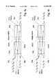
- FIGS., 4a through 4can optical device is shown in accordance with the invention embodying a free-space device wherein unguided collimated light propagates within the device.
- the interleaver/de-interleaver shownhas two glass interferometric end plates 42 having a spacer disposed therebetween.
- the spacer region between the two interferometric end plates 42has a 50/50 coating (shown) except for where a dotted line is shown.
- This dotted linerepresents the region between the plates 42 where the etalon is formed (not shown in detail) of two at least partially reflecting surfaces having an air gap there between having a predetermined dimension of >5 ⁇ defining the free spectral range of the etalon.
- Graded index (GRIN) lenses 40a, through 40c in FIGS. 4a and 4bserve to provide collimated light through and between the end plates 42, and serve as focusing lenses at output ports.
- Mirrors 41a and 41bare disposed at ends of the plates 42 to direct the beam toward a particular port. For example, light launched into an input port at lens 40a is directed at the etalon between the plates. About 50% of the light is transmitted through the front end of the etalon and follows a path wherein the light is incident upon the mirror 41a and it is subsequently directed to the lens 41b; the remaining light is transmitted through the back side of the etalon and impinges upon the mirror 41b where it is subsequently directed to the port at lens 40c.
- channels having centre wavelengths ⁇ 1, ⁇ 2, ⁇ 3, ⁇ 4, . . . ⁇ nare launched into the port at lens 40a, the channels are de-interleaved at the ports at lenses 40b and 40c into channel groups ⁇ 1, ⁇ 3, ⁇ 5 and ⁇ 2, ⁇ 4, ⁇ 6 . . . respectively; thereby providing two de-interleaved groups.
- FIG. 4billustrates how the same circuit of FIG. 4a can be used backwards to interleave de-interleaved channels.
- FIG. 4cillustrates that an extra input port at GRIN lens 40d can be added and the circuit can be used to switch input channels to either output port by appropriately adjusting and controlling the phase.
- an optical devicein accordance with the invention embodying a free-space device wherein unguided collimated light propagates within the device.
- the interleaver/de-interleaver shownhas two glass interferometric end plates 42 having a spacer disposed therebetween. The end plates and the spacer are joined by optical contacting. These contacting surfaces are polished simultaneously and in the same orientation in order to keep their surfaces parallel within 10 arc seconds when assembled.
- the axis of the through hole of the interferometric combiner and the axis of the coating B on each of the interferometric endplatesare concentric within 0.1 mm.
- the interferometric combineris conveniently embodied by a 50/50 coating. The etalon is absent this coating.
- Temperature sensors 52are shown at ends of the plates 52 to determine the relative temperature difference between the two interferometric end plates 42. Heaters 42a and 42b which are conveniently wrapped around the end plates 42 are used with the temperature sensors 52 to control the phase relationship between the transmitted and reflected optical signals passing through opposite ends of the etalon.
- FIG. 6Another embodiment of the invention is shown in FIG. 6, where an odd-integer number multi-cavity etalon is shown used in a same manner as was the single etalon described heretofore.
- multi-cavitiesi.e. three etalons
- the profile shown if FIG. 6ais acquired wherein there is an increase in the phase at certain portions 62 of the graph which result in a steeper sharper output response.
- multi-cavitiesi.e. three etalons
- FIG. 6billustrates two plots, one in dotted outline, which represents a portion of an output spectrum for a single cavity etalon and a solid line which represents the same portion of the output spectrum for a three cavity etalon device, in accordance with the invention.
- FIG. 6cillustrates the circuit in accordance with this invention having a multi-cavity etalon coupled to a combiner.
- the phase shifterhas ensured an effective phase difference of ⁇ /2, so that the phase shift incurred through the 50/50 splitter has been compensated. This, then, has allowed complete constructive and destructive interference to occur in the interferometer outputs.
- a different phase differenceis used, then with a certain combination of reflectivities for the two facets of the etalon, a linearized intensity variation with wavelength as shown in the graph of FIG. 7 can be achieved.
- the reflection coefficientsare 0.01 and 0.6 and the phase difference is 0.
- FIG. 8illustrates and alternative embodiment whereby a flat filter pass band is provided by using the correct phase difference and reflectivities.
- the etalon or multi-cavlity etaloncan be a tunable etalon.
Landscapes
- Physics & Mathematics (AREA)
- General Physics & Mathematics (AREA)
- Optics & Photonics (AREA)
- Mechanical Light Control Or Optical Switches (AREA)
- Spectrometry And Color Measurement (AREA)
Abstract
Description
Output from port 3: E.sub.R e.sup.jθR +E.sub.T e.sup.j(θT-π/2)
Output from port 2: E.sub.T e.sup.jθT +E.sub.R e.sup.j(θR-π/2)
I.sub.Res =1/2(E.sub.R.sup.2 +E.sub.T.sup.2 +2E.sub.R E.sub.T COS(Δθ))
Output from port 3: E.sub.R e.sup.jθR +E.sub.T e.sup.j(θT)
Output from port 2: E.sub.T e.sup.j(θT+π/2) +E.sub.R e.sup.j(θR-π/2)
Claims (23)
Priority Applications (6)
| Application Number | Priority Date | Filing Date | Title |
|---|---|---|---|
| CA 2278358CA2278358A1 (en) | 1998-12-23 | 1999-07-22 | Asymmetric interleaver/de-interleaver circuit |
| US09/358,445US6281977B1 (en) | 1998-12-23 | 1999-07-22 | Interferometric optical device including an optical resonator |
| CA 2292153CA2292153A1 (en) | 1998-12-23 | 1999-12-15 | Interferometric optical device including an optical resonator |
| JP11362881AJP2000231063A (en) | 1998-12-23 | 1999-12-21 | Interference type optical device including optical resonator |
| EP99310454AEP1016884A3 (en) | 1998-12-23 | 1999-12-22 | Interferometric optical device including an optical resonator |
| US09/871,822US6339474B2 (en) | 1998-12-23 | 2001-06-04 | Interferometric optical device including an optical resonator |
Applications Claiming Priority (2)
| Application Number | Priority Date | Filing Date | Title |
|---|---|---|---|
| CA2256963 | 1998-12-23 | ||
| CA002256963ACA2256963A1 (en) | 1998-12-23 | 1998-12-23 | Three port resonant optical cavity |
Related Child Applications (1)
| Application Number | Title | Priority Date | Filing Date |
|---|---|---|---|
| US33892599AContinuation-In-Part | 1998-12-23 | 1999-06-23 |
Publications (1)
| Publication Number | Publication Date |
|---|---|
| US6125220Atrue US6125220A (en) | 2000-09-26 |
Family
ID=4163119
Family Applications (1)
| Application Number | Title | Priority Date | Filing Date |
|---|---|---|---|
| US09/275,962Expired - LifetimeUS6125220A (en) | 1998-12-23 | 1999-03-25 | Interferometric optical device including a resonant optical cavity |
Country Status (2)
| Country | Link |
|---|---|
| US (1) | US6125220A (en) |
| CA (1) | CA2256963A1 (en) |
Cited By (44)
| Publication number | Priority date | Publication date | Assignee | Title |
|---|---|---|---|---|
| WO2001019007A1 (en)* | 1999-09-08 | 2001-03-15 | Chorum Technologies Lp | Apparatus for wavelength demultiplexing using a multi-cavity etalon |
| US6222958B1 (en)* | 1999-07-22 | 2001-04-24 | Jds Fitel Inc. | Optical interleaver/de-interleaver |
| US6252716B1 (en)* | 1999-07-22 | 2001-06-26 | Jds Uniphase Photonics C.V. | Bulk optic interleaver |
| US6268951B1 (en)* | 1999-06-29 | 2001-07-31 | Jds Uniphase Corporation | Optical signal interleaver/deinterleavers |
| US6281977B1 (en)* | 1998-12-23 | 2001-08-28 | Jds Fitel Inc. | Interferometric optical device including an optical resonator |
| US20020126291A1 (en)* | 2000-12-16 | 2002-09-12 | Qian Charles X. W. | Spectrum division multiplexing for high channel count optical networks |
| US6519065B1 (en)* | 1999-11-05 | 2003-02-11 | Jds Fitel Inc. | Chromatic dispersion compensation device |
| US6553158B1 (en)* | 1999-11-23 | 2003-04-22 | Lnl Technologies, Inc. | Tunable resonator having a movable phase shifter |
| US6611342B2 (en) | 2001-01-08 | 2003-08-26 | Optellios, Inc. | Narrow band polarization encoder |
| US20030174336A1 (en)* | 2002-03-15 | 2003-09-18 | Robert Te Kolste | Compact interferometer and use in wavelength monitoring |
| US20030223682A1 (en)* | 2002-05-30 | 2003-12-04 | Susumu Kinoshita | Optical add/drop node and method |
| US20030223670A1 (en)* | 2002-05-30 | 2003-12-04 | Anguel Nikolov | Optical polarization beam combiner/splitter |
| US6661950B1 (en) | 2001-01-10 | 2003-12-09 | Nomadics, Inc. | Microresonator-based tuned optical filter |
| US6678093B1 (en) | 2001-03-15 | 2004-01-13 | Cierra Photonics, Inc. | Optically coupled etalons and methods of making and using same |
| US6683721B2 (en) | 2001-02-27 | 2004-01-27 | Jds Uniphase Corporation | Low dispersion interleaver |
| WO2002059666A3 (en)* | 2000-12-27 | 2004-02-26 | Optoplex Corp | The application of an interferometer with a steplike phase difference between its arms in optical communication |
| US20040047638A1 (en)* | 2002-06-17 | 2004-03-11 | Jian Wang | Method and system for performing wavelength locking of an optical transmission source |
| US20040047388A1 (en)* | 2002-06-17 | 2004-03-11 | Jian Wang | Optical device and method for making same |
| US20040071425A1 (en)* | 2002-10-09 | 2004-04-15 | Jian Wang | Monolithic tunable lasers and reflectors |
| US20040071180A1 (en)* | 2002-10-09 | 2004-04-15 | Jian Wang | Freespace tunable optoelectronic device and method |
| US20040091212A1 (en)* | 1999-10-06 | 2004-05-13 | Strecker Brian N. | System, probe and methods for colorimetric testing |
| US20040111160A1 (en)* | 2001-07-18 | 2004-06-10 | Evans David L. | Prosthetic devices employing oxidized zirconium and other abrasion resistant surfaces contacting surfaces of cross-linked polyethylene |
| US6791758B1 (en) | 2001-03-15 | 2004-09-14 | Cierra Photonics Inc. | Optical etalons and methods of making and using them |
| US6798553B1 (en) | 2001-03-15 | 2004-09-28 | Bookham Technology Plc | Optical filter elements and methods of making and using same |
| US20040208505A1 (en)* | 2002-03-27 | 2004-10-21 | Susumu Kinoshita | Method and system for testing during operation of an open ring optical network |
| US20040258355A1 (en)* | 2003-06-17 | 2004-12-23 | Jian Wang | Micro-structure induced birefringent waveguiding devices and methods of making same |
| US6859303B2 (en) | 2002-06-18 | 2005-02-22 | Nanoopto Corporation | Optical components exhibiting enhanced functionality and method of making same |
| US6896949B1 (en) | 2001-03-15 | 2005-05-24 | Bookham (Us) Inc. | Wafer scale production of optical elements |
| US6907167B2 (en) | 2001-01-19 | 2005-06-14 | Gazillion Bits, Inc. | Optical interleaving with enhanced spectral response and reduced polarization sensitivity |
| US20050165667A1 (en)* | 2004-01-27 | 2005-07-28 | Cox George C. | System and method for customer video authentication to prevent identity theft |
| US20050201659A1 (en)* | 2004-03-11 | 2005-09-15 | Strecker Brian N. | System, probe and methods for colorimetric testing |
| US20050270544A1 (en)* | 2004-06-04 | 2005-12-08 | Optoplex Corporation | Variable dispersion step-phase interferometers |
| US20060045528A1 (en)* | 2004-08-27 | 2006-03-02 | Fujitsu Network Communications, Inc. | System and method for modularly scalable architecture for optical networks |
| US7050233B2 (en) | 2002-08-01 | 2006-05-23 | Nanoopto Corporation | Precision phase retardation devices and method of making same |
| US7116905B2 (en) | 2002-03-27 | 2006-10-03 | Fujitsu Limited | Method and system for control signaling in an open ring optical network |
| US20060279819A1 (en)* | 2005-05-26 | 2006-12-14 | Inphase Technologies, Inc. | Laser mode stabilization using an etalon |
| US7231148B2 (en) | 2002-03-28 | 2007-06-12 | Fujitsu Limited | Flexible open ring optical network and method |
| US20070297053A1 (en)* | 2003-02-10 | 2007-12-27 | Jian Wang | Universal broadband polarizer, devices incorporating same, and method of making same |
| US20140176951A1 (en)* | 2011-08-18 | 2014-06-26 | Kun Liu | Multi-band multiplexing intra-cavity gas sensing system and method |
| CN108897099A (en)* | 2018-08-31 | 2018-11-27 | 天津大学 | A kind of full polarization fiber interference type comb filter |
| US10547406B2 (en) | 2016-07-11 | 2020-01-28 | Fujitsu Limited | Optical element |
| US11126018B2 (en)* | 2017-12-07 | 2021-09-21 | Intel Corporation | Polarization de-multiplexing for intensity-modulated direct-detection (IM-DD) optical communications |
| CN115685536A (en)* | 2021-07-22 | 2023-02-03 | 朗美通经营有限责任公司 | High-precision optical locking device |
| US20230106876A1 (en)* | 2021-10-01 | 2023-04-06 | Lumentum Operations Llc | Bidirectional filter |
Citations (6)
| Publication number | Priority date | Publication date | Assignee | Title |
|---|---|---|---|---|
| US4680767A (en)* | 1985-07-01 | 1987-07-14 | Polaroid Corporation | Optical fiber laser |
| US4813756A (en)* | 1988-01-25 | 1989-03-21 | Bell Communications Research, Inc. | Etalon filters for optical channel selection in wavelength division multiplexed fiber systems |
| US5140651A (en)* | 1991-06-27 | 1992-08-18 | The United States Of America As Represented By The Secretary Of The Air Force | Semiconductive guided-wave programmable optical delay lines using electrooptic fabry-perot elements |
| US5283845A (en)* | 1992-07-20 | 1994-02-01 | Jds Fitel Inc. | Multi-port tunable fiber-optic filter |
| US5647036A (en)* | 1994-09-09 | 1997-07-08 | Deacon Research | Projection display with electrically-controlled waveguide routing |
| US5682447A (en)* | 1994-09-22 | 1997-10-28 | Washington State University Research Foundation | Photomechanical positioning and stabilization method and devices using optical fibers and feedback |
- 1998
- 1998-12-23CACA002256963Apatent/CA2256963A1/ennot_activeAbandoned
- 1999
- 1999-03-25USUS09/275,962patent/US6125220A/ennot_activeExpired - Lifetime
Patent Citations (7)
| Publication number | Priority date | Publication date | Assignee | Title |
|---|---|---|---|---|
| US4680767A (en)* | 1985-07-01 | 1987-07-14 | Polaroid Corporation | Optical fiber laser |
| US4813756A (en)* | 1988-01-25 | 1989-03-21 | Bell Communications Research, Inc. | Etalon filters for optical channel selection in wavelength division multiplexed fiber systems |
| US5140651A (en)* | 1991-06-27 | 1992-08-18 | The United States Of America As Represented By The Secretary Of The Air Force | Semiconductive guided-wave programmable optical delay lines using electrooptic fabry-perot elements |
| US5283845A (en)* | 1992-07-20 | 1994-02-01 | Jds Fitel Inc. | Multi-port tunable fiber-optic filter |
| US5647036A (en)* | 1994-09-09 | 1997-07-08 | Deacon Research | Projection display with electrically-controlled waveguide routing |
| US5724463A (en)* | 1994-09-09 | 1998-03-03 | Deacon Research | Projection display with electrically controlled waveguide-routing |
| US5682447A (en)* | 1994-09-22 | 1997-10-28 | Washington State University Research Foundation | Photomechanical positioning and stabilization method and devices using optical fibers and feedback |
Non-Patent Citations (4)
| Title |
|---|
| "Realizing of OADM using FP resonator as both dropping and bypass device" H. Naigqian, C. Zhangyuan, X. Anshi, X. Linzhen Conference on Optical Fiber Communication, Jul. 1998, vol. 3420, pp. 265-272. |
| Benjamin B. Dingel and Masayuki Izutsu, "Multifunction optical filter with a Michelson-Gires-Tournois interferometer for wavelength-division-multiplexed network system applications," Optical Society of America, 1998, 3 pp. |
| Benjamin B. Dingel and Masayuki Izutsu, Multifunction optical filter with a Michelson Gires Tournois interferometer for wavelength division multiplexed network system applications, Optical Society of America, 1998, 3 pp.* |
| Realizing of OADM using FP resonator as both dropping and bypass device H. Naigqian, C. Zhangyuan, X. Anshi, X. Linzhen Conference on Optical Fiber Communication, Jul. 1998, vol. 3420, pp. 265 272.* |
Cited By (73)
| Publication number | Priority date | Publication date | Assignee | Title |
|---|---|---|---|---|
| US6208444B1 (en)* | 1996-10-29 | 2001-03-27 | Chorum Technologies Inc. | Apparatus for wavelength demultiplexing using a multi-cavity etalon |
| US6281977B1 (en)* | 1998-12-23 | 2001-08-28 | Jds Fitel Inc. | Interferometric optical device including an optical resonator |
| US6339474B2 (en)* | 1998-12-23 | 2002-01-15 | Jds Uniphase Inc. | Interferometric optical device including an optical resonator |
| US6268951B1 (en)* | 1999-06-29 | 2001-07-31 | Jds Uniphase Corporation | Optical signal interleaver/deinterleavers |
| US6222958B1 (en)* | 1999-07-22 | 2001-04-24 | Jds Fitel Inc. | Optical interleaver/de-interleaver |
| US6252716B1 (en)* | 1999-07-22 | 2001-06-26 | Jds Uniphase Photonics C.V. | Bulk optic interleaver |
| WO2001019007A1 (en)* | 1999-09-08 | 2001-03-15 | Chorum Technologies Lp | Apparatus for wavelength demultiplexing using a multi-cavity etalon |
| US20040091212A1 (en)* | 1999-10-06 | 2004-05-13 | Strecker Brian N. | System, probe and methods for colorimetric testing |
| US7266271B2 (en) | 1999-10-06 | 2007-09-04 | Nomadics, Inc. | System, probe and methods for colorimetric testing |
| US6654564B1 (en)* | 1999-11-05 | 2003-11-25 | Jds Uniphase Inc. | Tunable dispersion compensator |
| US6519065B1 (en)* | 1999-11-05 | 2003-02-11 | Jds Fitel Inc. | Chromatic dispersion compensation device |
| US6768874B1 (en)* | 1999-11-05 | 2004-07-27 | Jds Fitel Inc. | Chromatic dispersion compensation device |
| US6553158B1 (en)* | 1999-11-23 | 2003-04-22 | Lnl Technologies, Inc. | Tunable resonator having a movable phase shifter |
| US20020126291A1 (en)* | 2000-12-16 | 2002-09-12 | Qian Charles X. W. | Spectrum division multiplexing for high channel count optical networks |
| WO2002059666A3 (en)* | 2000-12-27 | 2004-02-26 | Optoplex Corp | The application of an interferometer with a steplike phase difference between its arms in optical communication |
| US6611342B2 (en) | 2001-01-08 | 2003-08-26 | Optellios, Inc. | Narrow band polarization encoder |
| US6661950B1 (en) | 2001-01-10 | 2003-12-09 | Nomadics, Inc. | Microresonator-based tuned optical filter |
| US6907167B2 (en) | 2001-01-19 | 2005-06-14 | Gazillion Bits, Inc. | Optical interleaving with enhanced spectral response and reduced polarization sensitivity |
| US6683721B2 (en) | 2001-02-27 | 2004-01-27 | Jds Uniphase Corporation | Low dispersion interleaver |
| US6678093B1 (en) | 2001-03-15 | 2004-01-13 | Cierra Photonics, Inc. | Optically coupled etalons and methods of making and using same |
| US6896949B1 (en) | 2001-03-15 | 2005-05-24 | Bookham (Us) Inc. | Wafer scale production of optical elements |
| US6798553B1 (en) | 2001-03-15 | 2004-09-28 | Bookham Technology Plc | Optical filter elements and methods of making and using same |
| US6791758B1 (en) | 2001-03-15 | 2004-09-14 | Cierra Photonics Inc. | Optical etalons and methods of making and using them |
| US7182784B2 (en) | 2001-07-18 | 2007-02-27 | Smith & Nephew, Inc. | Prosthetic devices employing oxidized zirconium and other abrasion resistant surfaces contacting surfaces of cross-linked polyethylene |
| US20040111160A1 (en)* | 2001-07-18 | 2004-06-10 | Evans David L. | Prosthetic devices employing oxidized zirconium and other abrasion resistant surfaces contacting surfaces of cross-linked polyethylene |
| US6943890B2 (en) | 2002-03-15 | 2005-09-13 | Digital Optics Corporation | Compact interferometer and use in wavelength monitoring |
| US20030174336A1 (en)* | 2002-03-15 | 2003-09-18 | Robert Te Kolste | Compact interferometer and use in wavelength monitoring |
| US20070206493A1 (en)* | 2002-03-27 | 2007-09-06 | Fujitsu Limited | Flexible Open Ring Optical Network and Method |
| US20070223371A1 (en)* | 2002-03-27 | 2007-09-27 | Fujitsu Limited | Flexible Open Ring Optical Network and Method |
| US7970278B2 (en) | 2002-03-27 | 2011-06-28 | Fujitsu Limited | Flexible open ring optical network and method |
| US7076163B2 (en) | 2002-03-27 | 2006-07-11 | Fujitsu Limited | Method and system for testing during operation of an open ring optical network |
| US7116905B2 (en) | 2002-03-27 | 2006-10-03 | Fujitsu Limited | Method and system for control signaling in an open ring optical network |
| US7957644B2 (en) | 2002-03-27 | 2011-06-07 | Fujitsu Limited | Flexible open ring optical network and method |
| US20040208505A1 (en)* | 2002-03-27 | 2004-10-21 | Susumu Kinoshita | Method and system for testing during operation of an open ring optical network |
| US7231148B2 (en) | 2002-03-28 | 2007-06-12 | Fujitsu Limited | Flexible open ring optical network and method |
| US20030223682A1 (en)* | 2002-05-30 | 2003-12-04 | Susumu Kinoshita | Optical add/drop node and method |
| US20050201656A1 (en)* | 2002-05-30 | 2005-09-15 | Anguel Nikolov | Optical polarization beam combiner/splitter |
| US6876784B2 (en) | 2002-05-30 | 2005-04-05 | Nanoopto Corporation | Optical polarization beam combiner/splitter |
| US20030223670A1 (en)* | 2002-05-30 | 2003-12-04 | Anguel Nikolov | Optical polarization beam combiner/splitter |
| US6842562B2 (en) | 2002-05-30 | 2005-01-11 | Fujitsu Network Communications, Inc. | Optical add/drop node and method |
| US7283571B2 (en) | 2002-06-17 | 2007-10-16 | Jian Wang | Method and system for performing wavelength locking of an optical transmission source |
| US20040047388A1 (en)* | 2002-06-17 | 2004-03-11 | Jian Wang | Optical device and method for making same |
| US7386205B2 (en) | 2002-06-17 | 2008-06-10 | Jian Wang | Optical device and method for making same |
| US20040047638A1 (en)* | 2002-06-17 | 2004-03-11 | Jian Wang | Method and system for performing wavelength locking of an optical transmission source |
| US6859303B2 (en) | 2002-06-18 | 2005-02-22 | Nanoopto Corporation | Optical components exhibiting enhanced functionality and method of making same |
| US7050233B2 (en) | 2002-08-01 | 2006-05-23 | Nanoopto Corporation | Precision phase retardation devices and method of making same |
| US7634165B2 (en) | 2002-10-09 | 2009-12-15 | Api Nanofabrication And Research Corp. | Monolithic tunable lasers and reflectors |
| US20050271091A1 (en)* | 2002-10-09 | 2005-12-08 | Jian Wang | Monolithic tunable lasers and reflectors |
| US6920272B2 (en) | 2002-10-09 | 2005-07-19 | Nanoopto Corporation | Monolithic tunable lasers and reflectors |
| US20040071425A1 (en)* | 2002-10-09 | 2004-04-15 | Jian Wang | Monolithic tunable lasers and reflectors |
| US7013064B2 (en) | 2002-10-09 | 2006-03-14 | Nanoopto Corporation | Freespace tunable optoelectronic device and method |
| US20040071180A1 (en)* | 2002-10-09 | 2004-04-15 | Jian Wang | Freespace tunable optoelectronic device and method |
| US20070297053A1 (en)* | 2003-02-10 | 2007-12-27 | Jian Wang | Universal broadband polarizer, devices incorporating same, and method of making same |
| US7545564B2 (en) | 2003-02-10 | 2009-06-09 | Api Nanofabrication And Research Corporation | Universal broadband polarizer, devices incorporating same, and method of making same |
| US20040258355A1 (en)* | 2003-06-17 | 2004-12-23 | Jian Wang | Micro-structure induced birefringent waveguiding devices and methods of making same |
| US20050165667A1 (en)* | 2004-01-27 | 2005-07-28 | Cox George C. | System and method for customer video authentication to prevent identity theft |
| US7212701B2 (en) | 2004-03-11 | 2007-05-01 | Nomadics, Inc. | Methods for measuring optical absorbance of a sample medium |
| US7177492B2 (en) | 2004-03-11 | 2007-02-13 | Nomadics, Inc. | System, probe and methods for colorimetric testing |
| US20050201659A1 (en)* | 2004-03-11 | 2005-09-15 | Strecker Brian N. | System, probe and methods for colorimetric testing |
| US20060239606A1 (en)* | 2004-03-11 | 2006-10-26 | Strecker Brian N | System, probe and methods for colorimetric testing |
| US20050270544A1 (en)* | 2004-06-04 | 2005-12-08 | Optoplex Corporation | Variable dispersion step-phase interferometers |
| US7450851B2 (en) | 2004-08-27 | 2008-11-11 | Fujitsu Limited | System and method for modularly scalable architecture for optical networks |
| US20060045528A1 (en)* | 2004-08-27 | 2006-03-02 | Fujitsu Network Communications, Inc. | System and method for modularly scalable architecture for optical networks |
| US20060279819A1 (en)* | 2005-05-26 | 2006-12-14 | Inphase Technologies, Inc. | Laser mode stabilization using an etalon |
| US20140176951A1 (en)* | 2011-08-18 | 2014-06-26 | Kun Liu | Multi-band multiplexing intra-cavity gas sensing system and method |
| US8934100B2 (en)* | 2011-08-18 | 2015-01-13 | Tianjin University | Multi-band multiplexing intra-cavity gas sensing system and method |
| US10547406B2 (en) | 2016-07-11 | 2020-01-28 | Fujitsu Limited | Optical element |
| US11126018B2 (en)* | 2017-12-07 | 2021-09-21 | Intel Corporation | Polarization de-multiplexing for intensity-modulated direct-detection (IM-DD) optical communications |
| US11754861B2 (en) | 2017-12-07 | 2023-09-12 | Intel Corporation | Polarization de-multiplexing for intensity-modulated direct-detection (IM-DD) optical communications |
| CN108897099A (en)* | 2018-08-31 | 2018-11-27 | 天津大学 | A kind of full polarization fiber interference type comb filter |
| CN115685536A (en)* | 2021-07-22 | 2023-02-03 | 朗美通经营有限责任公司 | High-precision optical locking device |
| US20230106876A1 (en)* | 2021-10-01 | 2023-04-06 | Lumentum Operations Llc | Bidirectional filter |
| US12001057B2 (en)* | 2021-10-01 | 2024-06-04 | Lumentum Operations Llc | Bidirectional filter |
Also Published As
| Publication number | Publication date |
|---|---|
| CA2256963A1 (en) | 2000-06-23 |
Similar Documents
| Publication | Publication Date | Title |
|---|---|---|
| US6125220A (en) | Interferometric optical device including a resonant optical cavity | |
| US6339474B2 (en) | Interferometric optical device including an optical resonator | |
| US6804467B2 (en) | Chromatic dispersion compensation device | |
| US6130971A (en) | Fiber optic dense wavelength division multiplexer with a phase differential method of wavelength separation utilizing a polarization beam splitter and a nonlinear interferometer | |
| US6222958B1 (en) | Optical interleaver/de-interleaver | |
| US6768874B1 (en) | Chromatic dispersion compensation device | |
| US6252716B1 (en) | Bulk optic interleaver | |
| US20040141685A1 (en) | Dispersion-compensated optical wavelength router | |
| CA2203729C (en) | Method and circuit for demultiplexing an optical signal | |
| US6907167B2 (en) | Optical interleaving with enhanced spectral response and reduced polarization sensitivity | |
| CA2387417C (en) | Multi-cavity resonator interferometer | |
| WO2002091045A2 (en) | Compact tunable optical wavelength interleaver | |
| EP1016884A2 (en) | Interferometric optical device including an optical resonator | |
| US20020126291A1 (en) | Spectrum division multiplexing for high channel count optical networks | |
| EP1030480A2 (en) | Configurable optical circuit | |
| US6678441B1 (en) | Multireflector fiber optic filter apparatus and method | |
| EP1126293A2 (en) | Multiplexing/demultiplexing optical circuit | |
| US20020064332A1 (en) | Optic fibre multiplexer-demultiplexer with flattened response | |
| US6785000B2 (en) | Bulk optical interferometer | |
| de Ridder et al. | Interleavers | |
| US6577398B1 (en) | Resonant optical cavity | |
| US20020094157A1 (en) | Polarization dependent filtering device utilizing a fabry-perot cavity | |
| US7418168B2 (en) | Optical add/drop module | |
| CA2278358A1 (en) | Asymmetric interleaver/de-interleaver circuit | |
| WO2001084200A2 (en) | Optical wdm device having polarization elements |
Legal Events
| Date | Code | Title | Description |
|---|---|---|---|
| AS | Assignment | Owner name:JDS FITEL INC., CANADA Free format text:ASSIGNMENT OF ASSIGNORS INTEREST;ASSIGNORS:COPNER, NIGEL;COLBOURNE, PAUL;PHILIPSON, JOSHUA B.J.;REEL/FRAME:009861/0140 Effective date:19990324 | |
| STCF | Information on status: patent grant | Free format text:PATENTED CASE | |
| FPAY | Fee payment | Year of fee payment:4 | |
| AS | Assignment | Owner name:JDS UNIPHASE INC., CANADA Free format text:MERGER;ASSIGNOR:JDS FITEL INC.;REEL/FRAME:015676/0001 Effective date:19990706 | |
| FPAY | Fee payment | Year of fee payment:8 | |
| REMI | Maintenance fee reminder mailed | ||
| FPAY | Fee payment | Year of fee payment:12 | |
| AS | Assignment | Owner name:JDS UNIPHASE CORPORATION, CALIFORNIA Free format text:ASSIGNMENT OF ASSIGNORS INTEREST;ASSIGNOR:JDS UNIPHASE INC.;REEL/FRAME:036087/0320 Effective date:20150626 | |
| AS | Assignment | Owner name:LUMENTUM OPERATIONS LLC, CALIFORNIA Free format text:ASSIGNMENT OF ASSIGNORS INTEREST;ASSIGNOR:JDS UNIPHASE CORPORATION;REEL/FRAME:036420/0340 Effective date:20150731 | |
| FEPP | Fee payment procedure | Free format text:PAYOR NUMBER ASSIGNED (ORIGINAL EVENT CODE: ASPN); ENTITY STATUS OF PATENT OWNER: LARGE ENTITY Free format text:PAYER NUMBER DE-ASSIGNED (ORIGINAL EVENT CODE: RMPN); ENTITY STATUS OF PATENT OWNER: LARGE ENTITY | |
| AS | Assignment | Owner name:LUMENTUM OPERATIONS LLC, CALIFORNIA Free format text:CORRECTIVE ASSIGNMENT TO CORRECT THE PATENTS LISTED ON PAGE A-A33 PREVIOUSLY RECORDED ON REEL 036420 FRAME 0340. ASSIGNOR(S) HEREBY CONFIRMS THE PATENT NUMBERS 7,868,247 AND 6,476,312 WERE LISTED IN ERROR AND SHOULD BE REMOVED;ASSIGNOR:JDS UNIPHASE CORPORATION;REEL/FRAME:037562/0513 Effective date:20150731 Owner name:LUMENTUM OPERATIONS LLC, CALIFORNIA Free format text:CORRECTIVE ASSIGNMENT TO CORRECT INCORRECT PATENTS 7,868,247 AND 6,476,312 ON PAGE A-A33 PREVIOUSLY RECORDED ON REEL 036420 FRAME 0340. ASSIGNOR(S) HEREBY CONFIRMS THE ASSIGNMENT;ASSIGNOR:JDS UNIPHASE CORPORATION;REEL/FRAME:037562/0513 Effective date:20150731 | |
| AS | Assignment | Owner name:LUMENTUM OPERATIONS LLC, CALIFORNIA Free format text:CORRECTIVE ASSIGNMENT TO CORRECT THE PATENTS LISTED ON PAGE A-A33 PATENT NUMBERS 7,868,247 AND 6,476,312 WERE LISTED IN ERROR AND SHOULD BE REMOVED. PREVIOUSLY RECORDED ON REEL 036420 FRAME 0340. ASSIGNOR(S) HEREBY CONFIRMS THE ASSIGNMENT;ASSIGNOR:JDS UNIPHASE CORPORATION;REEL/FRAME:037627/0641 Effective date:20150731 Owner name:LUMENTUM OPERATIONS LLC, CALIFORNIA Free format text:CORRECTIVE ASSIGNMENT TO CORRECT PATENTS 7,868,247 AND 6,476,312 LISTED ON PAGE A-A33 PREVIOUSLY RECORDED ON REEL 036420 FRAME 0340. ASSIGNOR(S) HEREBY CONFIRMS THE ASSIGNMENT;ASSIGNOR:JDS UNIPHASE CORPORATION;REEL/FRAME:037627/0641 Effective date:20150731 | |
| FEPP | Fee payment procedure | Free format text:PAYER NUMBER DE-ASSIGNED (ORIGINAL EVENT CODE: RMPN); ENTITY STATUS OF PATENT OWNER: LARGE ENTITY Free format text:PAYOR NUMBER ASSIGNED (ORIGINAL EVENT CODE: ASPN); ENTITY STATUS OF PATENT OWNER: LARGE ENTITY | |
| AS | Assignment | Owner name:DEUTSCHE BANK AG NEW YORK BRANCH, AS COLLATERAL AGENT, NEW YORK Free format text:PATENT SECURITY AGREEMENT;ASSIGNORS:LUMENTUM OPERATIONS LLC;OCLARO FIBER OPTICS, INC.;OCLARO, INC.;REEL/FRAME:047788/0511 Effective date:20181210 Owner name:DEUTSCHE BANK AG NEW YORK BRANCH, AS COLLATERAL AG Free format text:PATENT SECURITY AGREEMENT;ASSIGNORS:LUMENTUM OPERATIONS LLC;OCLARO FIBER OPTICS, INC.;OCLARO, INC.;REEL/FRAME:047788/0511 Effective date:20181210 | |
| AS | Assignment | Owner name:OCLARO FIBER OPTICS, INC., CALIFORNIA Free format text:RELEASE BY SECURED PARTY;ASSIGNOR:DEUTSCHE AG NEW YORK BRANCH;REEL/FRAME:051287/0556 Effective date:20191212 Owner name:LUMENTUM OPERATIONS LLC, CALIFORNIA Free format text:RELEASE BY SECURED PARTY;ASSIGNOR:DEUTSCHE AG NEW YORK BRANCH;REEL/FRAME:051287/0556 Effective date:20191212 Owner name:OCLARO, INC., CALIFORNIA Free format text:RELEASE BY SECURED PARTY;ASSIGNOR:DEUTSCHE AG NEW YORK BRANCH;REEL/FRAME:051287/0556 Effective date:20191212 |